ICGOO在线商城 > 集成电路(IC) > 线性 - 音頻放大器 > TFA9882UK/N1,023

 Datasheet下载
- 型号: TFA9882UK/N1,023
- 制造商: NXP Semiconductors
- 库位|库存: xxxx|xxxx
- 要求:
| 数量阶梯 | 香港交货 | 国内含税 |
| +xxxx | $xxxx | ¥xxxx |
查看当月历史价格
查看今年历史价格
TFA9882UK/N1,023产品简介:
ICGOO电子元器件商城为您提供TFA9882UK/N1,023由NXP Semiconductors设计生产,在icgoo商城现货销售,并且可以通过原厂、代理商等渠道进行代购。 TFA9882UK/N1,023价格参考。NXP SemiconductorsTFA9882UK/N1,023封装/规格:线性 - 音頻放大器, Amplifier IC 1-Channel (Mono) Class D 9-WLCSP (1.49x1.27)。您可以下载TFA9882UK/N1,023参考资料、Datasheet数据手册功能说明书,资料中有TFA9882UK/N1,023 详细功能的应用电路图电压和使用方法及教程。
NXP USA Inc. 的 TFA9882UK/N1,023 是一款高性能的数字输入D类音频放大器,属于线性-音频放大器类别。该芯片主要应用于需要高音质、小尺寸和低功耗的便携式消费电子产品。

典型应用场景包括智能手机、平板电脑、超薄笔记本电脑以及高端无线耳机和智能音箱等设备。TFA9882采用I²S/PCM数字音频输入接口,支持立体声或单声道配置,具备高效能功率输出,能够在小尺寸扬声器中实现清晰、高动态范围的声音重放。

其集成的智能音频处理技术(如扬声器保护、自适应音量控制和动态范围压缩)可有效防止扬声器过载损坏,并在不同音量下保持音质稳定。此外,该芯片支持与NXP的音频软件生态系统配合使用,便于厂商进行音效调校和优化。

由于其封装小巧(WLCSP)、功耗低且无需外部散热设计,特别适合空间受限的移动设备。同时,TFA9882还具备良好的EMI抑制能力,有助于通过电磁兼容认证,提升产品整体可靠性。

综上所述,TFA9882UK/N1,023广泛适用于追求高保真音频体验的现代智能终端设备,是中高端消费类电子产品中理想的音频放大解决方案。
| 参数 | 数值 |
| 产品目录 | 集成电路 (IC) |
| 描述 | IC AMP AUDIO CLASSD 3.4W 9WLCSP |
| 产品分类 | |
| 品牌 | NXP Semiconductors |
| 数据手册 | |
| 产品图片 |
|
| 产品型号 | TFA9882UK/N1,023 |
| rohs | 无铅 / 符合限制有害物质指令(RoHS)规范要求 |
| 产品系列 | - |
| 不同负载时的最大输出功率x通道数 | 3.4W x 1 @ 4 欧姆 |
| 供应商器件封装 | 9-WLCSP(1.49x1.27) |
| 其它名称 | 568-6693-6 |
| 包装 | Digi-Reel® |
| 安装类型 | 表面贴装 |
| 封装/外壳 | 9-UFBGA,WLCSP |
| 工作温度 | -40°C ~ 85°C (TA) |
| 标准包装 | 1 |
| 特性 | 无噪声,I²S,静音,过电压,短路,热保护,欠电压 |
| 电压-电源 | 2.5 V ~ 5.5 V |
| 类型 | D 类 |
| 输出类型 | 1-通道(单声道) |


- 商务部:美国ITC正式对集成电路等产品启动337调查
- 曝三星4nm工艺存在良率问题 高通将骁龙8 Gen1或转产台积电
- 太阳诱电将投资9.5亿元在常州建新厂生产MLCC 预计2023年完工
- 英特尔发布欧洲新工厂建设计划 深化IDM 2.0 战略
- 台积电先进制程称霸业界 有大客户加持明年业绩稳了
- 达到5530亿美元!SIA预计今年全球半导体销售额将创下新高
- 英特尔拟将自动驾驶子公司Mobileye上市 估值或超500亿美元
- 三星加码芯片和SET,合并消费电子和移动部门,撤换高东真等 CEO
- 三星电子宣布重大人事变动 还合并消费电子和移动部门
- 海关总署:前11个月进口集成电路产品价值2.52万亿元 增长14.8%


PDF Datasheet 数据手册内容提取
TFA9882 3.4 W I2S input mono class-D audio amplifier Rev. 2 — 20 April 2011 Product data sheet 1. General description The TFA9882 is a mono, filter-free class-D audio amplifier in a 9-bump WLCSP (Wafer Level Chip-Size Package) with a 400 μm pitch. It receives audio and control settings via an I2S digital interface. The Power-down to Operating mode transition is triggered when a clock signal is detected on the bit clock input (BCK). Two devices can be combined to build a stereo application. In stereo applications, the left or right I2S audio stream is selected by connecting the word select signal to, respectively, pin WSL or pin WSR. Mono mixing can be achieved by connecting the word select signal to both WSL and WSR. Switching off the word select signal selects Mute mode. The device features low RF susceptibility because it has a digital input interface that is insensitive to clock jitter. The second order closed loop architecture used in the TFA9882 provides excellent audio performance and high supply voltage ripple rejection. 2. Features and benefits (cid:132) Small outline WLCSP9 package: 1.27 × 1.49 × 0.6 mm (cid:132) Wide supply voltage range (fully operational from 2.5 V to 5.5 V) (cid:132) High efficiency (90 %, 4 Ω/20 μH load) and low power dissipation (cid:132) Quiescent power: (cid:139)6.5 mW (V =1.8 V, V =3.6 V, 4 Ω/20 μH load, f =32 kHz) DDD DDP s (cid:139)7.65 mW (V =1.8 V, V =3.6 V, 4 Ω/20 μH load, f =48 kHz) DDD DDP s (cid:132) Output power: (cid:139)1.4 W into 4 Ω at 3.6 V supply (THD = 1%) (cid:139)2.7 W into 4 Ω at 5.0 V supply (THD = 1%) (cid:139)3.4 W into 4 Ω at 5.0 V supply (THD = 10%) (cid:132) Output noise voltage: 24 μV (A-weighted) (cid:132) Signal-to-noise ratio: 103 dB (V =5 V, A-weighted) DDP (cid:132) Fully short-circuit proof across load and to supply lines (cid:132) Current limiting to avoid audio holes (cid:132) Thermally protected (cid:132) Undervoltage and overvoltage protection (cid:132) High-pass filter for DC blocking (cid:132) Simplified interface for audio and control settings (cid:132) Left/right selection and mono mixing (cid:132) Three gain settings: −3dB, 0dB and +3dB
TFA9882 NXP Semiconductors 3.4 W I2S input mono class-D audio amplifier (cid:132) Output slope setting for EMI reduction (cid:132) Clip control for smooth clipping (cid:132) Mute mode (cid:132) Low RF susceptibility (cid:132) Insensitive to input clock jitter (cid:132) ‘Pop noise' free at all mode transitions (cid:132) Short power-up time: 4 ms (cid:132) Short power-down time: 5 μs (cid:132) 1.8 V/3.3 V tolerant digital inputs (cid:132) Only two external components required 3. Applications (cid:132) PDAs (cid:132) Mobile phones (cid:132) Portable gaming devices (cid:132) Portable Navigation Devices (PND) (cid:132) Notebooks/netbooks (cid:132) Portable media players 4. Quick reference data Table 1. Quick reference data All parameters are guaranteed for V = 3.6 V;V =1.8 V; R = 4 Ω[1]; L = 20μH[1]; f =1kHz; DDP DDD L L i f = 48 kHz; T = 25°C; default settings, unless otherwise specified. s amb Symbol Parameter Conditions Min Typ Max Unit V power supply voltage on pin V 2.5 - 5.5 V DDP DDP V digital supply voltage on pin V 1.65 1.8 1.95 V DDD DDD I power supply current Operating mode with load - 1.5 1.7 mA DDP Mute mode - 1.1 1.25 mA Power-down mode - 0.1 1 μA I digital supply current Operating mode - 1.25 1.4 mA DDD Mute mode - 1.1 1.2 mA Power-down mode - 2.5 10 μA BCK=WS=DATA = 0 V P RMS output power THD + N = 1 % o(RMS) V = 3.6 V, f = 100 Hz - 1.4 - W DDP i V = 5.0 V, f = 100 Hz - 2.7 - W DDP i THD + N = 10 % V = 3.6 V, f = 100 Hz - 1.75 - W DDP i V = 5.0 V, f = 100 Hz - 3.4 - W DDP i η output power efficiency P =1.4 W - 90 - % po o(RMS) [1] R =load resistance; L =load inductance. L L TFA9882 All information provided in this document is subject to legal disclaimers. © NXP B.V. 2011. All rights reserved. Product data sheet Rev. 2 — 20 April 2011 2 of 31
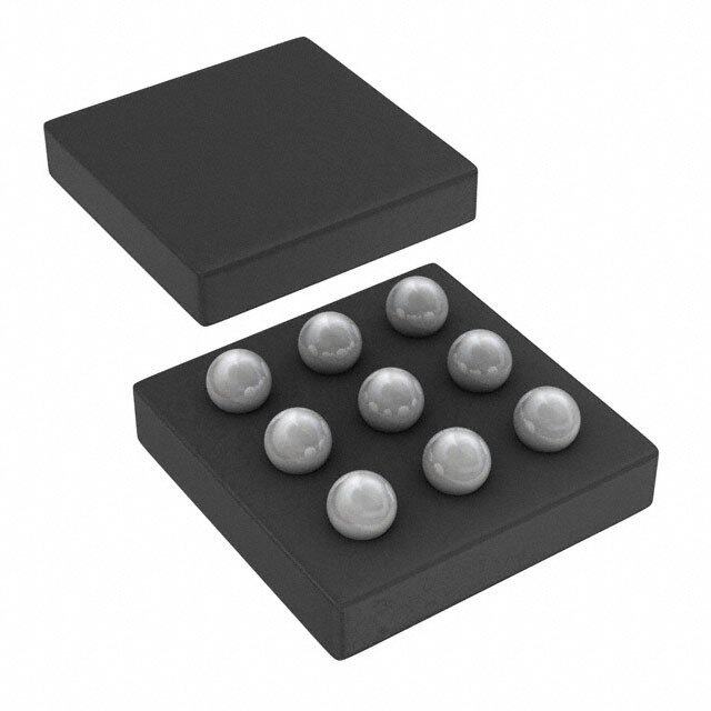
TFA9882 NXP Semiconductors 3.4 W I2S input mono class-D audio amplifier 5. Ordering information Table 2. Ordering info rmation Type number Package Name Description Version TFA9882UK WLCSP9 wafer level chip-size package; 9 bumps; body 1.49 × 1.27 mm TFA9882UK 6. Block diagram VDDD VDDP B1 B2 MUTE CONTROL TFA9882 LEFT/RIGHT SELECTION WSL A2 C3 OUTA WSR C2 I2S HP DATA A1 RECEIVER FILTER PWM H-BRIDGE BCK C1 A3 OUTB PROTECTION POWER DOWN CIRCUITS: CONTROL OTP OVP UVP OCP B3 GND 010aaa724 Fig 1. Block diagram of the TFA9882 TFA9882 All information provided in this document is subject to legal disclaimers. © NXP B.V. 2011. All rights reserved. Product data sheet Rev. 2 — 20 April 2011 3 of 31
TFA9882 NXP Semiconductors 3.4 W I2S input mono class-D audio amplifier 7. Pinning information 7.1 Pinning TFA9882 TFA9882 bump A1 1 2 3 index area 1 2 3 C A B B A C bump A1 010aaa725 010aaa726 index area Bottom view Transparent top view Fig 2. Bump configuration for WLCSP9 (bottom view) Fig 3. Bump configuration for WLCSP9 (top view) 1 2 3 A DATA WSL OUTB B VDDD VDDP GND C BCK WSR OUTA 010aaa727 Transparent top view Fig 4. Bump mapping for WLCSP9 7.2 Pin description Table 3. Pin description Symbol Pin Type Description DATA A1 I data input WSL A2 I word select input left channel; connect to V or PCB DDP ground if right channel is selected OUTB A3 O inverting output V B1 P digital supply voltage (1.8 V) DDD V B2 P power supply voltage (2.5 V to 5.5 V) DDP GND B3 P ground reference BCK C1 I bit clock input WSR C2 I word select input right channel; connect to V or PCB DDP ground if left channel is selected OUTA C3 O non-inverting output TFA9882 All information provided in this document is subject to legal disclaimers. © NXP B.V. 2011. All rights reserved. Product data sheet Rev. 2 — 20 April 2011 4 of 31
TFA9882 NXP Semiconductors 3.4 W I2S input mono class-D audio amplifier 8. Functional description The TFA9882 is a high-efficiency mono Bridge Tied Load (BTL) class-D audio amplifier with a digital stereo I2S input interface. A High-Pass (HP) filter removes the DC components from the incoming I2S stream. This stream is subsequently converted into two Pulse Width Modulated (PWM) signals. A 3-level PWM scheme supports filterless speaker drive. 8.1 Mode selection and interfacing The TFA9882 supports four operating modes: • Power-down mode, with low supply current • Mute mode, in which the output stages are floating so that the audio input signal is suppressed • Operating mode, in which the amplifier is fully operational, delivering an output signal • Fault mode The TFA9882 switches to Fault mode automatically when a protection mechanism is activated (see Section8.8). The defined patterns required on the BCK, WSL and WSR inputs to select the other three modes are given in Table4. Power-down mode is selected when there is no bit clock signal on the BCK input. Applying the bit clock signal will cause the TFA9882 to switch from Power-down mode to Operating mode (provided the word select signal is switched on). Mute mode is activated when the word select signal is switched off. The left or right channel is selected by applying the word select signal to, respectively, the WSL or the WSR terminal. The word select terminal not connected should be connected to V or to PCB ground. This simplifies the connection to the V terminal in the DDP DDP WLCSP9 package. When the word select signal is connected to both terminals, the TFA9882 amplifies the sum of both channels divided by two. Table 4. Mode selecti on Mode Channel Frequency on BCK Frequency on WSL Frequency on WSR OUTA, OUTB Power-down 0 Hz don’t care don’t care floating Mute 2.048 MHz to 3.072 MHz 0 Hz 0 Hz floating Operating left 2.048 MHz to 3.072 MHz 32 kHz to 48 kHz 0 Hz switching right 2.048 MHz to 3.072 MHz 0 Hz 32 kHz to 48 kHz switching (left+right)/2 2.048 MHz to 3.072 MHz 32 kHz to 48 kHz 32 kHz to 48 kHz switching TFA9882 All information provided in this document is subject to legal disclaimers. © NXP B.V. 2011. All rights reserved. Product data sheet Rev. 2 — 20 April 2011 5 of 31
TFA9882 NXP Semiconductors 3.4 W I2S input mono class-D audio amplifier 8.2 I2S format The TFA9882 supports the Philips I2S standard with a BCK frequency 64 times greater than the sampling rate (64fs). The bit length can be from 8 to 32 bits. Supported I2S sample rates are listed in Table5 while Figure5 illustrates the I2S data transfer format. Table 5. Supported I2S sample rates f (kHz) WS (kHz) BCK, 64f (MHz) s s 32 32 2.048 44.1 44.1 2.8224 48 48 3.072 WS LEFT RIGHT 1 2 3 1 2 3 BCK DATA MSB B2 MSB B2 MSB 010aaa728 I2S-BUS FORMAT MSB=Most Significant Bit; B2 = Second Most Significant Bit Fig 5. I2S format 8.3 Power-up/power-down sequence The TFA9882 power-up/power-down sequence is shown in Figure 6. External power supplies V and V should be within their operating limits before the TFA9882 DDP DDD switches to Operating mode. The TFA9882 should be switched to Power-down mode before the power supplies are disconnected or turned off. VDDD, VDDP BCK 64·fs clock signal WS 1·fs clock signal no clock signal 1·fs clock signal OUTA, switching floating switching OUTB td(on) Operating Mute Operating td(off) 010aaa729 Fig 6. Power-up/power-down timing (without control settings) TFA9882 All information provided in this document is subject to legal disclaimers. © NXP B.V. 2011. All rights reserved. Product data sheet Rev. 2 — 20 April 2011 6 of 31
TFA9882 NXP Semiconductors 3.4 W I2S input mono class-D audio amplifier Table 6. Power-up/power-down timing All parameters are guaranteed for V = 3.6 V;V =1.8 V; R = 4 Ω[1]; L = 20μH[1]; f =1kHz; DDP DDD L L i f = 48 kHz; T = 25°C; default settings, unless otherwise specified. s amb Symbol Parameter Conditions Min Typ Max Unit t turn-on delay time [2] - - 4 ms d(on) t turn-off delay time [2] - - 5 μs d(off) [1] R =load resistance; L =load inductance. L L [2] Inversely proportional to f . s 8.4 Control settings If the device can operate effectively with the default settings, the control settings don’t need to be changed. 8.4.1 Control setting pattern recognition The TFA9882 can detect control settings via the I2S input. Control settings are selected by transmitting control patterns on the DATA input during the power-up sequence (the first 12288 bit clock cycles). The word select signal (WS) must be switched off during this interval. Figure7 illustrates the control setting sequence. After receiving 128 consecutive control setting bytes, the TFA9882 activates the appropriate control setting (see the third column of Table7). Control settings remain unchanged in all modes unless control pattern 0xAA is received or the V supply voltage is removed. DDD Power-down Control settings I2S data WS 1 2 3 12288 BCK DATA MSB B2 LSB MSB B2 LSB MSB B2 LSB MSB B2 LSB td(on) 010aaa731 LSB = Least Significant Bit; MSB=Most Significant Bit; B2 = Second Most Significant Bit Fig 7. Power-up/power-down timing (without control settings) Table 7. Control settings Byte Related bytes[1] Control settings 0xD2 0x69/B4/5A/2D/96/4B/A5 clip control on; see Section8.4.2 0xD4 0x6A/35/9A/4D/A6/53/A9 gain=−3 dB (V =2.5 V); see Section8.4.3 DDP 0xD8 0x6C/36/1B/8D/C6/63/B1 gain=+3 dB (V =5.0 V); see Section8.4.3 DDP 0xE1 0xF0/78/3C/1E/0F/87/C3 slope low (EMC); see Section8.4.4 0xE2 0x71/B8/5C/2E/17/8B/C5 Dynamic Power Stage Activation (DPSA) off; see Section8.4.5 0xAA 0x55 Default; no mute, reset settings to default [1] The related bytes are the bytes from the first column phase shifted by 1, 2, 3, 4, 5, 6 and 7 bits. TFA9882 All information provided in this document is subject to legal disclaimers. © NXP B.V. 2011. All rights reserved. Product data sheet Rev. 2 — 20 April 2011 7 of 31
TFA9882 NXP Semiconductors 3.4 W I2S input mono class-D audio amplifier 8.4.2 Clip control TFA9882 clip control is off by default. Clip control can be turned on via control setting 0xD2 (see Section8.4.1). The TFA9882 clips smoothly with clip control on. Output power is at maximum with clip control off. 8.4.3 Gain selection Signal conversion from digital audio to PWM modulated audio out is independent of supply voltages V and V . At the default gain setting (0 dB), the audio output signal DDP DDD level is just below the clipping point at a supply voltage of 3.6 V at −6dBFS (peak) input. The TFA9882 supports two further gain settings to support full output power at V =2.5V and V = 5.0 V. The gain settings can be selected via control settings DDP DDP 0xD4 and 0xD8 (see Section8.4.1). Table8 details the corresponding peak output voltage level at −6dBFS for the three gain settings. Table 8. Output volta ge All parameters are guaranteed for V = 3.6 V; V =1.8 V; R = 4 Ω[1], L =20 μH[1], f =1 kHz, f =48 kHz, T =25 °C, DDP DDD L L i s amb default settings; unless otherwise specified. Symbol Parameter Conditions Min Typ Max Unit V peak output voltage at −6dBFS (peak) digital input oM gain = −3dB, V = 2.5 V, R = 4 Ω [1] - 2.4 - V DDP L gain = 0dB, V = 3.6 V, R = 4 Ω; default [1] - 3.4 - V DDP L gain = +3 dB, V = 5.0 V, R = 8 Ω [1] - 4.7 - V DDP L [1] R =load resistance; L =load inductance. L L 8.4.4 PWM slope selection The rise and fall times of the PWM output edges can be set to one of two values, as detailed in Table9. The default setting is ‘slope normal’ (10 ns with V =3.6 V). ‘Slope DDP low’ is selected via control setting 0xE1 (see Section8.4.1). This function is implemented to reduce ElectroMagnetic Interference (EMI). Table 9. Slope rise and fall times Setting Rise and fall times of the PWM output edges slope low 40 ns with V =3.6 V DDP slope normal; default setting 10 ns with V =3.6 V DDP 8.4.5 Dynamic Power Stage Activation (DPSA) The TFA9882 uses DPSA to regulate current consumption in line with the level of the incoming audio stream. This function switches off power stage sections that are not needed, reducing current consumption. Each of the TFA9882 H-bridge power stages is divided into eight sections. The number of power stage sections activated depends on the level of the incoming audio stream. The thresholds used by the DPSA to determine how many stages are switched on are given in Table10. The DPSA signal is used as a reference signal for switching power stage sections on and off. The DPSA signal will rise in tandem with the rectified audio input signal. When the rectified audio input signal falls, the DPSA decreases with a negative exponential function, as illustrated in Figure8. TFA9882 All information provided in this document is subject to legal disclaimers. © NXP B.V. 2011. All rights reserved. Product data sheet Rev. 2 — 20 April 2011 8 of 31
TFA9882 NXP Semiconductors 3.4 W I2S input mono class-D audio amplifier The DPSA function can be switched off via control setting 0xE2 (see Section8.4.1). When DPSA is off, all power stage sections are activated in Operating mode. Table 10. DPSA input levels Setting Number of power stage sections active ≤ 0.035 ×full scale (−29 dBFS) 1 > 0.035 ×full scale (−29 dBFS) 2 > 0.07 ×full scale (−23 dBFS) 4 > 0.105 ×full scale (−19.5 dBFS) 8 DPSA signal 0.105 × full scale 0.07 × full scale 0.035 × full scale 1 section 8 sections 4 sections 2 sections 010aaa713 Fig 8. Dynamic Power Stage Activation 8.5 High-pass filter The high-pass filter blocks the DC components in the incoming audio stream. The cut-off frequency, f , is determined by the sampling frequency, f , and is defined in high(−3dB) s Equation1: –f ⋅ ln(4095⁄4096) f = ------s------------------------------------------- (1) high(–3dB) 2⋅π f is about 1.9 Hz at a sampling frequency of 48 kHz. The high-pass filter is always high(−3dB) enabled. 8.6 PWM frequency The TFA9882 translates the I2S input stream into an amplified 3-level PWM output signal. The PWM switching frequency is linearly proportional to the sampling frequency, and is defined in Equation2. f = 8⋅f (2) sw(PWM) s The PWM switching frequency equals 384 kHz when the sampling frequency is 48 kHz. TFA9882 All information provided in this document is subject to legal disclaimers. © NXP B.V. 2011. All rights reserved. Product data sheet Rev. 2 — 20 April 2011 9 of 31
TFA9882 NXP Semiconductors 3.4 W I2S input mono class-D audio amplifier 8.7 Bandwidth The TFA9882 output spectrum has a sigma-delta converter characteristic. Figure9 illustrates the output power spectrum of the TFA9882 when it is receiving an I2S input stream without audio content. The quantization noise is shaped above the band of interest. The band of interest (bandwidth) is determined by the high corner frequency where the noise is increasing. The bandwidth in Figure9 scales with the sampling frequency and is defined in Equation3: BW = 0.4535⋅f (3) s −40 010aaa709 output (dBFS) −80 −120 −160 10 102 103 104 105 106 f (Hz) Fig 9. Output power spectrum, f = 48 kHz s 8.8 Protection mechanisms The following protection circuits are included in the TFA9882: • OverTemperature Protection (OTP) • OverVoltage Protection (OVP) • UnderVoltage Protection (UVP) • OverCurrent Protection (OCP) The reaction of the device to fault conditions differs depending on the protection circuit involved. 8.8.1 OverTemperature Protection (OTP) OTP prevents heat damage to the TFA9882. It is triggered when the junction temperature exceeds T . When this happens, the output stages are set floating. OTP is cleared act(th_prot) automatically via an internal timer (200 ms), after which the output stages will start to operate normally again. TFA9882 All information provided in this document is subject to legal disclaimers. © NXP B.V. 2011. All rights reserved. Product data sheet Rev. 2 — 20 April 2011 10 of 31
TFA9882 NXP Semiconductors 3.4 W I2S input mono class-D audio amplifier 8.8.2 Supply voltage protection mechanisms (UVP and OVP) UVP is activated, setting the outputs floating, if the supply voltage drops below the undervoltage protection threshold, V . This transition will be silent, without pop noise. P(uvp) When the supply voltage rises above V again, the system will be restarted after P(uvp) 200ms. OVP is activated, setting the power stages floating, if the supply voltage rises above the overvoltage protection threshold, V . The power stages are re-enabled as soon as the P(ovp) supply voltage drops below V again. The system will be restarted after 200ms. P(ovp) 8.8.3 OverCurrent Protection (OCP) OCP will detect a short circuit across the load or between one of the amplifier outputs and one of the supply lines. If the output current exceeds the overcurrent protection threshold (I ), it will be limited to I while the amplifier outputs are switching (the amplifier is O(ocp) O(ocp) not powered down completely). This is called current limiting. The amplifier can distinguish between an impedance drop at the loudspeaker and a low-ohmic short circuit across the load or to one of the supply lines. The impedance threshold depends on which supply voltage is being used: • In the event of a short circuit across the load or a short to one of the supply lines, the audio amplifier is switched off completely. It will try to restart again after approximately 200 ms. If the short-circuit condition is still present after this time, this cycle will be repeated. Average dissipation will be low because of the short duty cycle. • In the event of an impedance drop (e.g. due to dynamic behavior of the loudspeaker), the same protection mechanism will be activated. The maximum output current is again limited to I , but the amplifier will not switch off completely (thus preventing O(ocp) audio holes from occurring). This will result in a clipped output signal without artifacts. TFA9882 All information provided in this document is subject to legal disclaimers. © NXP B.V. 2011. All rights reserved. Product data sheet Rev. 2 — 20 April 2011 11 of 31
TFA9882 NXP Semiconductors 3.4 W I2S input mono class-D audio amplifier 9. Internal circuitry Table 11. Internal circuitry Pin Symbol Equivalent circuit A1 DATA C1 BCK A1, C1 ESD B3 010aaa714 B1 V DDD B1, B2 B2 V DDP ESD B3 010aaa715 A2 WSL B2 C2 WSR A2, C2 ESD B3 010aaa716 A3 OUTB B2 C3 OUTA A3, C3 B3 010aaa717 10. Limiting values Table 12. Limiting valu es In accordance with the Absolute Maximum Rating System (IEC 60134). Symbol Parameter Conditions Min Max Unit V power supply voltage on pin V −0.3 +5.5 V DDP DDP V digital supply voltage on pin V −0.3 +1.95 V DDD DDD T junction temperature - +150 °C j T storage temperature −55 +150 °C stg T ambient temperature −40 +85 °C amb V voltage on pin x pins BCK and DATA −0.3 +3.6 V x pins OUTA and OUTB −0.6 V + 0.6 V DDP pins WSL and WSR −0.6 V V DDP TFA9882 All information provided in this document is subject to legal disclaimers. © NXP B.V. 2011. All rights reserved. Product data sheet Rev. 2 — 20 April 2011 12 of 31
TFA9882 NXP Semiconductors 3.4 W I2S input mono class-D audio amplifier Table 12. Limiting values …continued In accordance with the Absolute Maximum Rating System (IEC 60134). Symbol Parameter Conditions Min Max Unit V electrostatic discharge voltage according to the Human Body Model (HBM) [1] ESD pins OUTA and OUTB −8 +8 kV any other pin −2 +2 kV according to the Charge Device Model (CDM) [1] −500 +500 V according to the Machine Model (MM) [1] −200 +200 V [1] Measurements taken on the TFA9882 in a HVSON10 package (engineering samples) due to handling restrictions with WLCSP9. 11. Thermal characteristics Table 13. Thermal cha racteristics Symbol Parameter Conditions Typ Unit R thermal resistance from junction to ambient in free air; natural convection th(j-a) JEDEC test board [1] 128 K/W 2-layer application board 97 K/W Ψ thermal characterization parameter from [2] 12 K/W j-top junction to top of package [1] Measured on a JEDEC high K-factor test board (standard EIA/JESD 51-7). [2] Value depends on where measurement is taken on package. 12. Characteristics 12.1 DC characteristics Table 14. DC characte ristics All parameters are guaranteed for V = 3.6 V;V =1.8 V; R = 4 Ω[1]; L = 20μH[1]; f = 1 kHz; f = 48 kHz; T = 25°C, DDP DDD L L i s amb default slope and gain settings; unless otherwise specified. Symbol Parameter Conditions Min Typ Max Unit V power supply voltage on pin V 2.5 - 5.5 V DDP DDP V digital supply voltage on pin V 1.65 1.8 1.95 V DDD DDD I power supply current Operating mode with load DDP f =48 kHz - 1.5 1.7 mA s f =32 kHz - 1.38 - mA s Mute mode 1.1 1.25 mA Power-down mode - 0.1 1 μA TFA9882 All information provided in this document is subject to legal disclaimers. © NXP B.V. 2011. All rights reserved. Product data sheet Rev. 2 — 20 April 2011 13 of 31
TFA9882 NXP Semiconductors 3.4 W I2S input mono class-D audio amplifier Table 14. DC characteristics …continued All parameters are guaranteed for V = 3.6 V;V =1.8 V; R = 4 Ω[1]; L = 20μH[1]; f = 1 kHz; f = 48 kHz; T = 25°C, DDP DDD L L i s amb default slope and gain settings; unless otherwise specified. Symbol Parameter Conditions Min Typ Max Unit I digital supply current Operating mode DDD f =48 kHz - 1.25 1.4 mA s f =32 kHz - 0.85 - mA s Mute mode f =48 kHz - 1.1 1.2 mA s f =32 kHz - 0.8 - mA s Power-down mode - 2.5 10 μA BCK = WS=DATA = 0 V Series resistance output power switches R drain-source on-state resistance - 125 150 mΩ DSon Amplifier output pins; pins OUTA and OUTB |V | output offset voltage - - 3 mV O(offset) BCK, DATA, WSL and WSR V HIGH-level input voltage 0.7V - 3.6 V IH DDD V LOW-level input voltage - - 0.3V V IL DDD C input capacitance - - 3 pF i Protection T thermal protection activation temperature 130 - 150 °C act(th_prot) V overvoltage protection supply voltage 5.5 - 6.0 V P(ovp) V undervoltage protection supply voltage 2.3 - 2.5 V P(uvp) I overcurrent protection output current 1.45 - - A O(ocp) [1] R =load resistance; L =load inductance. L L TFA9882 All information provided in this document is subject to legal disclaimers. © NXP B.V. 2011. All rights reserved. Product data sheet Rev. 2 — 20 April 2011 14 of 31
TFA9882 NXP Semiconductors 3.4 W I2S input mono class-D audio amplifier 12.2 AC characteristics Table 15. AC characte ristics All parameters are guaranteed for V = 3.6 V;V =1.8 V; R = 4 Ω[1]; L = 20μH[1]; f = 1 kHz; f = 48 kHz; T = 25°C, DDP DDD L L i s amb default slope and gain settings; unless otherwise specified. Symbol Parameter Conditions Min Typ Max Unit Output power P RMS output power THD + N = 1 % o(RMS) V = 3.6 V, f = 100 Hz - 1.4 - W DDP i V = 5.0 V, f = 100 Hz - 2.7 - W DDP i THD + N = 1 %; R = 8 Ω; L = 44μH L L V = 3.6 V, f = 100 Hz - 0.75 - W DDP i V = 5.0 V, f = 100 Hz - 1.45 - W DDP i THD + N = 10 % V = 3.6 V, f = 100 Hz - 1.75 - W DDP i V = 5.0 V, f = 100 Hz - 3.4 - W DDP i THD + N = 10 %; R = 8 Ω; L = 44μH L L V = 3.6 V, f = 100 Hz - 0.95 - W DDP i V = 5.0 V, f = 100 Hz - 1.85 - W DDP i Performance η output power efficiency P = 1.4 W - 90 - % po o(RMS) THD+N total harmonic distortion-plus-noise P = 100 mW - 0.02 0.1 % o(RMS) V output noise voltage A-weighted - 24 - μV n(o) S/N signal-to-noise ratio V =5 V; V = 3.4V (RMS); A-weighted - 103 - dB DDP o PSRR power supply rejection ratio V =200 mV; f =217 Hz - 85 - dB ripple ripple V peak output voltage at −6dBFS (peak) digital input: oM gain=−3 dB; V =2.5 V - 2.3 - V DDP gain=0 dB; V =3.6 V 3.1 3.3 3.5 V DDP gain=+3 dB; V =5.0 V; R =8 Ω - 4.7 - V DDP L Power-up, power-down and propagation times t turn-on delay time [2] - - 4 ms d(on) t turn-off delay time [2] - - 5 μs d(off) t propagation delay [2] - 600 - μs PD [1] R =load resistance; L =load inductance. L L [2] Inversely proportional to f . s TFA9882 All information provided in this document is subject to legal disclaimers. © NXP B.V. 2011. All rights reserved. Product data sheet Rev. 2 — 20 April 2011 15 of 31
TFA9882 NXP Semiconductors 3.4 W I2S input mono class-D audio amplifier 12.3 I2S timing characteristics Table 16. I2S timing ch aracteristics All parameters are guaranteed for V = 3.6 V;V =1.8 V; R = 4 Ω[1]; L = 20μH[1]; f = 1 kHz; f = 48 kHz; T = 25°C, DDP DDD L L i s amb default slope and gain settings; unless otherwise specified. Symbol Parameter Conditions Min Typ Max Unit f sampling frequency on pins WSL or WSR 32 - 48 kHz s f clock frequency on pin BCK - 64f - Hz clk s t set-up time WS edge to BCK HIGH 10 - - ns su DATA edge to BCK HIGH 10 - - ns t hold time BCK HIGH to WS edge 10 - - ns h BCK HIGH to DATA edge 10 - - ns [1] R =load resistance; L =load inductance. L L BCK th tsu WS DATA 010aaa732 Fig 10. I2S timing TFA9882 All information provided in this document is subject to legal disclaimers. © NXP B.V. 2011. All rights reserved. Product data sheet Rev. 2 — 20 April 2011 16 of 31
TFA9882 NXP Semiconductors 3.4 W I2S input mono class-D audio amplifier 13. Application information 13.1 ElectroMagnetic Compatibility (EMC) EMC standards define to what degree a (sub)system is susceptible to externally imposed electromagnetic influences and to what degree a (sub)system is responsible for emitting electromagnetic signals, when in Standby mode or Operating mode. EMC immunity and emission values are normally measured over a frequency range from 180 kHz up to 3 GHz. 13.1.1 Immunity A major reason why amplifier devices pick up high frequency signals, and (after detection) manifest these in the device's audio band, is the presence of analog circuits inside the device or in the (sub)system. The TFA9882 has digital inputs and digital outputs. Comparative tests on a TFA9882-based (sub)system show that the impact of externally imposed electromagnetic signals on the device is negligible in both Standby and Operating modes. 13.1.2 Emissions Since the TFA9882 is a class-D amplifier with digitally switched outputs in a BTL configuration, it can potentially generate emissions due to the steep edges on the amplifier outputs. External components can be used to suppress these emissions. However, the TFA9882 features built-in slope control to suppress such emissions by reducing the slew rate of the BTL output signals. By reducing the slew rate, the emissions are reduced by some 10dB when compared with full-speed operation. 13.2 Supply decoupling and filtering A ceramic decoupling capacitor of between 4.7 μF and 10 μF should be placed close to the TFA9882 for decoupling the V supply. This minimizes the size of the DDP high-frequency current loop, thereby optimizing EMC performance. TFA9882 All information provided in this document is subject to legal disclaimers. © NXP B.V. 2011. All rights reserved. Product data sheet Rev. 2 — 20 April 2011 17 of 31
TFA9882 NXP Semiconductors 3.4 W I2S input mono class-D audio amplifier 13.3 Typical application diagram (simplified) battery WSL WSR VDDP A2 C2 B2 DATA A1 OUTA C3 BCK C1 TFA9882UK left speaker 4 Ω or 8 Ω 1.8 V VDDD B1 A3 OUTB B3 BASEBAND CVDDD D CVDDP 100 nF N 4.7 μF PROCESSOR G I2S output battery WSL WSR VDDP A2 C2 B2 DATA A1 OUTA C3 BCK C1 TFA9882UK right speaker 4 Ω or 8 Ω 1.8 V VDDD B1 A3 OUTB B3 CVDDD D CVDDP 100 nF N 4.7 μF G 010aaa733 Fig 11. Typical stereo application (simplified) TFA9882 All information provided in this document is subject to legal disclaimers. © NXP B.V. 2011. All rights reserved. Product data sheet Rev. 2 — 20 April 2011 18 of 31
TFA9882 NXP Semiconductors 3.4 W I2S input mono class-D audio amplifier 13.4 Curves measured in reference design (demonstration board) All measurements were taken with V =1.8V, f =6.144 MHz, clip control off, DPSA DDD clk off and slope normal, unless otherwise specified. 102 001aam634 102 001aam636 THD+N THD+N (%) (%) 10 10 1 1 10−1 (1) 10−1 (1) (3) 10−2 10−2 (2) (2) (3) 10−3 10−3 10−3 10−2 10−1 1 10 10−3 10−2 10−1 1 10 Po (W) Po (W) (1) f = 6 kHz. (1) f = 6 kHz. i i (2) f = 1 kHz. (2) f = 1 kHz. i i (3) f = 100 Hz. (3) f = 100 Hz. i i a. V =3.6V,R =8Ω, L =44 μH b. V =5V,R =8Ω, L =44 μH DDP L L DDP L L 102 001aam633 102 001aam635 THD+N THD+N (%) (%) 10 10 1 1 (1) 10−1 10−1 (1) (3) (3) 10−2 (2) 10−2 (2) 10−3 10−3 10−3 10−2 10−1 1 10 10−3 10−2 10−1 1 10 Po (W) Po (W) (1) f = 6 kHz. (1) f = 6 kHz. i i (2) f = 1 kHz. (2) f = 1 kHz. i i (3) f = 100 Hz. (3) f = 100 Hz. i i c. V =3.6V,R =4Ω, L =20 μH d. V =5V,R =4Ω, L =20 μH DDP L L DDP L L Fig 12. THD+N as a function of output power TFA9882 All information provided in this document is subject to legal disclaimers. © NXP B.V. 2011. All rights reserved. Product data sheet Rev. 2 — 20 April 2011 19 of 31
TFA9882 NXP Semiconductors 3.4 W I2S input mono class-D audio amplifier 001aam638 001aam640 10 10 THD+N THD+N (%) (%) 1 1 10−1 10−1 (1) (1) 10−2 (2) 10−2 (2) 10−3 10−3 10 102 103 104 105 10 102 103 104 105 fi (Hz) fi (Hz) (1) P = 500 mW (1) P = 500 mW o o (2) P = 100 mW (2) P = 100 mW o o a. V =3.6V,R =8Ω, L =44 μH b. V =5V,R =8Ω, L =44 μH DDP L L DDP L L 001aam637 001aam639 10 10 THD+N THD+N (%) (%) 1 1 10−1 10−1 (1) (1) (2) 10−2 (2) 10−2 10−3 10−3 10 102 103 104 105 10 102 103 104 105 fi (Hz) fi (Hz) (1) P = 1W (1) P = 1W o o (2) P = 100 mW (2) P = 100 mW o o c. V =3.6V,R =4Ω, L =20 μH d. V =5V,R =4Ω, L =20 μH DDP L L DDP L L Fig 13. THD+N as a function of frequency TFA9882 All information provided in this document is subject to legal disclaimers. © NXP B.V. 2011. All rights reserved. Product data sheet Rev. 2 — 20 April 2011 20 of 31
TFA9882 NXP Semiconductors 3.4 W I2S input mono class-D audio amplifier 001aam641 001aam642 10 10 THD+N+IMD THD+N+IMD (%) (%) 1 1 10−1 (4) 10−1 (4) (3) (3) 10−2 ((21)) 10−2 ((21)) 10−3 10−3 10 102 103 104 105 10 102 103 104 105 fi (Hz) fi (Hz) (1) V = 0 V (f = 0 Hz) (1) V = 0 V (f = 0 Hz) ripple ripple ripple ripple (2) f = 217 Hz (2) f = 217 Hz ripple ripple (3) f = 1 kHz (3) f = 1 kHz ripple ripple (4) f = 6 kHz (4) f = 6 kHz ripple ripple a. V =3.6V,R =4Ω, L =20 μH, P =100 mW b. V =5V,R =4Ω, L =20 μH, P =100 mW DDP L L o DDP L L o V =200 mV (RMS) V =200mV (RMS) ripple ripple Fig 14. THD+N + power supply intermodulation distortion as a function of frequency 4 001aan660 −10 001aam644 G (1) PSRR (dB) (dB) −30 2 −50 (2) 0 −70 (1) -2 −90 (2) (3) -4 −110 10 102 103 104 105 10 102 103 104 105 fi (Hz) fripple (Hz) (1) gain=+3 dB (1) V = 3.6V DDP (2) gain=0 dB (2) V = 5V DDP (3) gain=−3 dB RL=4Ω, LL=20 μH, Vripple=200mV (RMS) VDDP=3.6V, RL=4 Ω, LL=20 μH, Po=500 mW Fig 15. Normalized gain as a function of frequency Fig 16. PSRR as a function of ripple frequency TFA9882 All information provided in this document is subject to legal disclaimers. © NXP B.V. 2011. All rights reserved. Product data sheet Rev. 2 — 20 April 2011 21 of 31
TFA9882 NXP Semiconductors 3.4 W I2S input mono class-D audio amplifier 001aam632 110 S/N ratio (dB) 90 (1) 70 (2) 50 30 10 10−3 10−2 10−1 1 10 Po (W) (1) A-weighted (2) 20 kHz brickwall filter VDDP=5V, RL=4Ω, LL=20 μH, reference signal: 3.4 V (RMS) Fig 17. S/N ratio as a function of output power 001aam649 001aam650 5 4 (PWo) Po (W) (1) 4 (1) 3 (2) (2) 3 2 (3) (3) 2 (4) (4) 1 1 0 0 2 3 4 5 6 2 3 4 5 6 VDDP (V) VDDP (V) (1) THD+N =10%, RL=4 Ω, LL=20 μH (1) THD+N =10%, RL=4 Ω, LL=20 μH (2) THD+N =1%, RL=4 Ω, LL=20 μH (2) THD+N =1%, RL=4 Ω, LL=20 μH (3) THD+N =10%, RL=8 Ω, LL=44 μH (3) THD+N =10%, RL=8 Ω, LL=44 μH (4) THD+N =1%, RL=8 Ω, LL=44 μH (4) THD+N =1%, RL=8 Ω, LL=44 μH a. f =100 Hz, clip control off b. f =100 Hz, clip control on i i Fig 18. Output power as a function of supply voltage TFA9882 All information provided in this document is subject to legal disclaimers. © NXP B.V. 2011. All rights reserved. Product data sheet Rev. 2 — 20 April 2011 22 of 31
TFA9882 NXP Semiconductors 3.4 W I2S input mono class-D audio amplifier 001aam647 001aam645 0.15 0.4 P P (W) (2) (W) (2) 0.3 0.10 0.2 (1) (1) 0.05 0.1 0 0 10−3 10−2 10−1 1 10 10−3 10−2 10−1 1 10 Po (W) Po (W) (1) V =3.6V (1) V =3.6V DDP DDP (2) V =5V (2) V =5V DDP DDP a. R =8 Ω, L =44 μH, f =1 kHz, DPSA on b. R =4 Ω, L =20 μH, f =1 kHz, DPSA on L L i L L i Fig 19. Power dissipation as a function of output power 001aam648 001aam646 100 100 η (1) (2) η (1) (2) (%) (%) 80 80 60 60 40 40 20 20 0 0 0 0.5 1.0 1.5 2.0 0 0.5 1.0 1.5 2.0 2.5 3.0 3.5 Po (W) Po (W) (1) V =3.6V (1) V =3.6V DDP DDP (2) V =5V (2) V =5V DDP DDP a. R =8 Ω, L =44 μH, f =1 kHz, DPSA on b. R =4 Ω, L =20 μH, f =1 kHz, DPSA on L L i L L i Fig 20. Efficiency as a function of output power TFA9882 All information provided in this document is subject to legal disclaimers. © NXP B.V. 2011. All rights reserved. Product data sheet Rev. 2 — 20 April 2011 23 of 31
TFA9882 NXP Semiconductors 3.4 W I2S input mono class-D audio amplifier 14. Package outline WLCSP9: wafer level chip-size package; 9 bumps; body 1.49 x 1.27 mm TFA9882UK D B A bump A1 index area A2 E A A1 detail X ZD1 ZD2 e1 C Ø v C A B e b Ø w C y C e B e1 A bump A1 index area 1 2 3 X 0 0.5 1 mm scale Dimensions Unit A A1 A2 b D E e e1 e2 v w y ZD1 ZD2 ZE max 0.6 0.22 0.38 0.28 1.521 1.301 0.465 0.285 0.265 mm nom 0.20 0.36 0.26 1.491 1.271 0.4 0.8 0.8 0.015 0.04 0.02 0.435 0.255 0.235 min 0.18 0.34 0.24 1.461 1.241 0.405 0.225 0.205 tfa9882uk_po Outline References European Issue date version IEC JEDEC JEITA projection 11-02-01 TFA9882UK 11-02-10 Fig 21. Package outline TFA9882UK (WLCSP9) TFA9882 All information provided in this document is subject to legal disclaimers. © NXP B.V. 2011. All rights reserved. Product data sheet Rev. 2 — 20 April 2011 24 of 31
TFA9882 NXP Semiconductors 3.4 W I2S input mono class-D audio amplifier 15. Soldering of WLCSP packages 15.1 Introduction to soldering WLCSP packages This text provides a very brief insight into a complex technology. A more in-depth account of soldering WLCSP (Wafer Level Chip-Size Packages) can be found in application note AN10439 “Wafer Level Chip Scale Package” and in application note AN10365 “Surface mount reflow soldering description”. Wave soldering is not suitable for this package. All NXP WLCSP packages are lead-free. 15.2 Board mounting Board mounting of a WLCSP requires several steps: 1. Solder paste printing on the PCB 2. Component placement with a pick and place machine 3. The reflow soldering itself 15.3 Reflow soldering Key characteristics in reflow soldering are: • Lead-free versus SnPb soldering; note that a lead-free reflow process usually leads to higher minimum peak temperatures (see Figure22) than a PbSn process, thus reducing the process window • Solder paste printing issues, such as smearing, release, and adjusting the process window for a mix of large and small components on one board • Reflow temperature profile; this profile includes preheat, reflow (in which the board is heated to the peak temperature), and cooling down. It is imperative that the peak temperature is high enough for the solder to make reliable solder joints (a solder paste characteristic) while being low enough that the packages and/or boards are not damaged. The peak temperature of the package depends on package thickness and volume and is classified in accordance with Table17. Table 17. Lead-free process (from J-STD-020C) Package thickness (mm) Package reflow temperature (°C) Volume (mm3) < 350 350 to 2000 > 2000 < 1.6 260 260 260 1.6 to 2.5 260 250 245 > 2.5 250 245 245 Moisture sensitivity precautions, as indicated on the packing, must be respected at all times. Studies have shown that small packages reach higher temperatures during reflow soldering, see Figure22. TFA9882 All information provided in this document is subject to legal disclaimers. © NXP B.V. 2011. All rights reserved. Product data sheet Rev. 2 — 20 April 2011 25 of 31
TFA9882 NXP Semiconductors 3.4 W I2S input mono class-D audio amplifier maximum peak temperature = MSL limit, damage level temperature minimum peak temperature = minimum soldering temperature peak temperature time 001aac844 MSL: Moisture Sensitivity Level Fig 22. Temperature profiles for large and small components For further information on temperature profiles, refer to application note AN10365 “Surface mount reflow soldering description”. 15.3.1 Stand off The stand off between the substrate and the chip is determined by: • The amount of printed solder on the substrate • The size of the solder land on the substrate • The bump height on the chip The higher the stand off, the better the stresses are released due to TEC (Thermal Expansion Coefficient) differences between substrate and chip. 15.3.2 Quality of solder joint A flip-chip joint is considered to be a good joint when the entire solder land has been wetted by the solder from the bump. The surface of the joint should be smooth and the shape symmetrical. The soldered joints on a chip should be uniform. Voids in the bumps after reflow can occur during the reflow process in bumps with high ratio of bump diameter to bump height, i.e. low bumps with large diameter. No failures have been found to be related to these voids. Solder joint inspection after reflow can be done with X-ray to monitor defects such as bridging, open circuits and voids. 15.3.3 Rework In general, rework is not recommended. By rework we mean the process of removing the chip from the substrate and replacing it with a new chip. If a chip is removed from the substrate, most solder balls of the chip will be damaged. In that case it is recommended not to re-use the chip again. TFA9882 All information provided in this document is subject to legal disclaimers. © NXP B.V. 2011. All rights reserved. Product data sheet Rev. 2 — 20 April 2011 26 of 31
TFA9882 NXP Semiconductors 3.4 W I2S input mono class-D audio amplifier Device removal can be done when the substrate is heated until it is certain that all solder joints are molten. The chip can then be carefully removed from the substrate without damaging the tracks and solder lands on the substrate. Removing the device must be done using plastic tweezers, because metal tweezers can damage the silicon. The surface of the substrate should be carefully cleaned and all solder and flux residues and/or underfill removed. When a new chip is placed on the substrate, use the flux process instead of solder on the solder lands. Apply flux on the bumps at the chip side as well as on the solder pads on the substrate. Place and align the new chip while viewing with a microscope. To reflow the solder, use the solder profile shown in application note AN10365 “Surface mount reflow soldering description”. 15.3.4 Cleaning Cleaning can be done after reflow soldering. TFA9882 All information provided in this document is subject to legal disclaimers. © NXP B.V. 2011. All rights reserved. Product data sheet Rev. 2 — 20 April 2011 27 of 31
TFA9882 NXP Semiconductors 3.4 W I2S input mono class-D audio amplifier 16. Revision history Table 18. Revision history Document ID Release date Data sheet status Change notice Supersedes TFA9882 v.2 20110420 Product data sheet TFA9882 v.1 Modifications: • Data sheet status changed to ‘Product data sheet’ TFA9882 v.1 20110331 Preliminary data sheet - - TFA9882 All information provided in this document is subject to legal disclaimers. © NXP B.V. 2011. All rights reserved. Product data sheet Rev. 2 — 20 April 2011 28 of 31
TFA9882 NXP Semiconductors 3.4 W I2S input mono class-D audio amplifier 17. Legal information 17.1 Data sheet status Document status[1][2] Product status[3] Definition Objective [short] data sheet Development This document contains data from the objective specification for product development. Preliminary [short] data sheet Qualification This document contains data from the preliminary specification. Product [short] data sheet Production This document contains the product specification. [1] Please consult the most recently issued document before initiating or completing a design. [2] The term ‘short data sheet’ is explained in section “Definitions”. [3] The product status of device(s) described in this document may have changed since this document was published and may differ in case of multiple devices. The latest product status information is available on the Internet at URLhttp://www.nxp.com. 17.2 Definitions malfunction of an NXP Semiconductors product can reasonably be expected to result in personal injury, death or severe property or environmental damage. NXP Semiconductors accepts no liability for inclusion and/or use of Draft — The document is a draft version only. The content is still under NXP Semiconductors products in such equipment or applications and internal review and subject to formal approval, which may result in therefore such inclusion and/or use is at the customer’s own risk. modifications or additions. NXP Semiconductors does not give any representations or warranties as to the accuracy or completeness of Applications — Applications that are described herein for any of these information included herein and shall have no liability for the consequences of products are for illustrative purposes only. NXP Semiconductors makes no use of such information. representation or warranty that such applications will be suitable for the specified use without further testing or modification. Short data sheet — A short data sheet is an extract from a full data sheet with the same product type number(s) and title. A short data sheet is intended Customers are responsible for the design and operation of their applications for quick reference only and should not be relied upon to contain detailed and and products using NXP Semiconductors products, and NXP Semiconductors full information. For detailed and full information see the relevant full data accepts no liability for any assistance with applications or customer product sheet, which is available on request via the local NXP Semiconductors sales design. It is customer’s sole responsibility to determine whether the NXP office. In case of any inconsistency or conflict with the short data sheet, the Semiconductors product is suitable and fit for the customer’s applications and full data sheet shall prevail. products planned, as well as for the planned application and use of customer’s third party customer(s). Customers should provide appropriate Product specification — The information and data provided in a Product design and operating safeguards to minimize the risks associated with their data sheet shall define the specification of the product as agreed between applications and products. NXP Semiconductors and its customer, unless NXP Semiconductors and NXP Semiconductors does not accept any liability related to any default, customer have explicitly agreed otherwise in writing. In no event however, damage, costs or problem which is based on any weakness or default in the shall an agreement be valid in which the NXP Semiconductors product is customer’s applications or products, or the application or use by customer’s deemed to offer functions and qualities beyond those described in the third party customer(s). Customer is responsible for doing all necessary Product data sheet. testing for the customer’s applications and products using NXP Semiconductors products in order to avoid a default of the applications and 17.3 Disclaimers the products or of the application or use by customer’s third party customer(s). NXP does not accept any liability in this respect. Limited warranty and liability — Information in this document is believed to Limiting values — Stress above one or more limiting values (as defined in be accurate and reliable. However, NXP Semiconductors does not give any the Absolute Maximum Ratings System of IEC60134) will cause permanent representations or warranties, expressed or implied, as to the accuracy or damage to the device. Limiting values are stress ratings only and (proper) completeness of such information and shall have no liability for the operation of the device at these or any other conditions above those given in consequences of use of such information. the Recommended operating conditions section (if present) or the Characteristics sections of this document is not warranted. Constant or In no event shall NXP Semiconductors be liable for any indirect, incidental, repeated exposure to limiting values will permanently and irreversibly affect punitive, special or consequential damages (including - without limitation - lost the quality and reliability of the device. profits, lost savings, business interruption, costs related to the removal or replacement of any products or rework charges) whether or not such Terms and conditions of commercial sale — NXP Semiconductors damages are based on tort (including negligence), warranty, breach of products are sold subject to the general terms and conditions of commercial contract or any other legal theory. sale, as published at http://www.nxp.com/profile/terms, unless otherwise Notwithstanding any damages that customer might incur for any reason agreed in a valid written individual agreement. In case an individual whatsoever, NXP Semiconductors’ aggregate and cumulative liability towards agreement is concluded only the terms and conditions of the respective customer for the products described herein shall be limited in accordance agreement shall apply. NXP Semiconductors hereby expressly objects to with the Terms and conditions of commercial sale of NXP Semiconductors. applying the customer’s general terms and conditions with regard to the purchase of NXP Semiconductors products by customer. Right to make changes — NXP Semiconductors reserves the right to make changes to information published in this document, including without No offer to sell or license — Nothing in this document may be interpreted or limitation specifications and product descriptions, at any time and without construed as an offer to sell products that is open for acceptance or the grant, notice. This document supersedes and replaces all information supplied prior conveyance or implication of any license under any copyrights, patents or to the publication hereof. other industrial or intellectual property rights. Suitability for use — NXP Semiconductors products are not designed, Export control — This document as well as the item(s) described herein authorized or warranted to be suitable for use in life support, life-critical or may be subject to export control regulations. Export might require a prior safety-critical systems or equipment, nor in applications where failure or authorization from national authorities. TFA9882 All information provided in this document is subject to legal disclaimers. © NXP B.V. 2011. All rights reserved. Product data sheet Rev. 2 — 20 April 2011 29 of 31
TFA9882 NXP Semiconductors 3.4 W I2S input mono class-D audio amplifier Quick reference data — The Quick reference data is an extract of the product for such automotive applications, use and specifications, and (b) product data given in the Limiting values and Characteristics sections of this whenever customer uses the product for automotive applications beyond document, and as such is not complete, exhaustive or legally binding. NXP Semiconductors’ specifications such use shall be solely at customer’s own risk, and (c) customer fully indemnifies NXP Semiconductors for any Non-automotive qualified products — Unless this data sheet expressly liability, damages or failed product claims resulting from customer design and states that this specific NXP Semiconductors product is automotive qualified, use of the product for automotive applications beyond NXP Semiconductors’ the product is not suitable for automotive use. It is neither qualified nor tested standard warranty and NXP Semiconductors’ product specifications. in accordance with automotive testing or application requirements. NXP Semiconductors accepts no liability for inclusion and/or use of non-automotive qualified products in automotive equipment or applications. 17.4 Trademarks In the event that customer uses the product for design-in and use in automotive applications to automotive specifications and standards, customer Notice: All referenced brands, product names, service names and trademarks (a) shall use the product without NXP Semiconductors’ warranty of the are the property of their respective owners. 18. Contact information For more information, please visit: http://www.nxp.com For sales office addresses, please send an email to: salesaddresses@nxp.com TFA9882 All information provided in this document is subject to legal disclaimers. © NXP B.V. 2011. All rights reserved. Product data sheet Rev. 2 — 20 April 2011 30 of 31
TFA9882 NXP Semiconductors 3.4 W I2S input mono class-D audio amplifier 19. Contents 1 General description. . . . . . . . . . . . . . . . . . . . . . 1 15.2 Board mounting . . . . . . . . . . . . . . . . . . . . . . . 25 2 Features and benefits . . . . . . . . . . . . . . . . . . . . 1 15.3 Reflow soldering . . . . . . . . . . . . . . . . . . . . . . 25 15.3.1 Stand off. . . . . . . . . . . . . . . . . . . . . . . . . . . . . 26 3 Applications. . . . . . . . . . . . . . . . . . . . . . . . . . . . 2 15.3.2 Quality of solder joint. . . . . . . . . . . . . . . . . . . 26 4 Quick reference data. . . . . . . . . . . . . . . . . . . . . 2 15.3.3 Rework. . . . . . . . . . . . . . . . . . . . . . . . . . . . . . 26 5 Ordering information. . . . . . . . . . . . . . . . . . . . . 3 15.3.4 Cleaning. . . . . . . . . . . . . . . . . . . . . . . . . . . . . 27 6 Block diagram . . . . . . . . . . . . . . . . . . . . . . . . . . 3 16 Revision history . . . . . . . . . . . . . . . . . . . . . . . 28 7 Pinning information. . . . . . . . . . . . . . . . . . . . . . 4 17 Legal information . . . . . . . . . . . . . . . . . . . . . . 29 7.1 Pinning . . . . . . . . . . . . . . . . . . . . . . . . . . . . . . . 4 17.1 Data sheet status. . . . . . . . . . . . . . . . . . . . . . 29 7.2 Pin description . . . . . . . . . . . . . . . . . . . . . . . . . 4 17.2 Definitions . . . . . . . . . . . . . . . . . . . . . . . . . . . 29 8 Functional description . . . . . . . . . . . . . . . . . . . 5 17.3 Disclaimers . . . . . . . . . . . . . . . . . . . . . . . . . . 29 8.1 Mode selection and interfacing. . . . . . . . . . . . . 5 17.4 Trademarks . . . . . . . . . . . . . . . . . . . . . . . . . . 30 8.2 I2S format . . . . . . . . . . . . . . . . . . . . . . . . . . . . . 6 18 Contact information . . . . . . . . . . . . . . . . . . . . 30 8.3 Power-up/power-down sequence. . . . . . . . . . . 6 19 Contents. . . . . . . . . . . . . . . . . . . . . . . . . . . . . . 31 8.4 Control settings. . . . . . . . . . . . . . . . . . . . . . . . . 7 8.4.1 Control setting pattern recognition . . . . . . . . . . 7 8.4.2 Clip control . . . . . . . . . . . . . . . . . . . . . . . . . . . . 8 8.4.3 Gain selection. . . . . . . . . . . . . . . . . . . . . . . . . . 8 8.4.4 PWM slope selection . . . . . . . . . . . . . . . . . . . . 8 8.4.5 Dynamic Power Stage Activation (DPSA). . . . . 8 8.5 High-pass filter . . . . . . . . . . . . . . . . . . . . . . . . . 9 8.6 PWM frequency . . . . . . . . . . . . . . . . . . . . . . . . 9 8.7 Bandwidth. . . . . . . . . . . . . . . . . . . . . . . . . . . . 10 8.8 Protection mechanisms . . . . . . . . . . . . . . . . . 10 8.8.1 OverTemperature Protection (OTP) . . . . . . . . 10 8.8.2 Supply voltage protection mechanisms (UVP and OVP) . . . . . . . . . . . . . . . . . . . . . . . 11 8.8.3 OverCurrent Protection (OCP) . . . . . . . . . . . . 11 9 Internal circuitry. . . . . . . . . . . . . . . . . . . . . . . . 12 10 Limiting values. . . . . . . . . . . . . . . . . . . . . . . . . 12 11 Thermal characteristics . . . . . . . . . . . . . . . . . 13 12 Characteristics. . . . . . . . . . . . . . . . . . . . . . . . . 13 12.1 DC characteristics . . . . . . . . . . . . . . . . . . . . . 13 12.2 AC characteristics. . . . . . . . . . . . . . . . . . . . . . 15 12.3 I2S timing characteristics . . . . . . . . . . . . . . . . 16 13 Application information. . . . . . . . . . . . . . . . . . 17 13.1 ElectroMagnetic Compatibility (EMC). . . . . . . 17 13.1.1 Immunity. . . . . . . . . . . . . . . . . . . . . . . . . . . . . 17 13.1.2 Emissions. . . . . . . . . . . . . . . . . . . . . . . . . . . . 17 13.2 Supply decoupling and filtering. . . . . . . . . . . . 17 13.3 Typical application diagram (simplified) . . . . . 18 13.4 Curves measured in reference design (demonstration board) . . . . . . . . . . . . . . . . . . 19 14 Package outline. . . . . . . . . . . . . . . . . . . . . . . . 24 15 Soldering of WLCSP packages. . . . . . . . . . . . 25 15.1 Introduction to soldering WLCSP packages. . 25 Please be aware that important notices concerning this document and the product(s) described herein, have been included in section ‘Legal information’. © NXP B.V. 2011. All rights reserved. For more information, please visit: http://www.nxp.com For sales office addresses, please send an email to: salesaddresses@nxp.com Date of release: 20 April 2011 Document identifier: TFA9882