ICGOO在线商城 > 集成电路(IC) > 线性 - 音頻放大器 > TAS5630BPHD
 Datasheet下载
- 型号: TAS5630BPHD
- 制造商: Texas Instruments
- 库位|库存: xxxx|xxxx
- 要求:
| 数量阶梯 | 香港交货 | 国内含税 |
| +xxxx | $xxxx | ¥xxxx |
查看当月历史价格
查看今年历史价格
TAS5630BPHD产品简介:
ICGOO电子元器件商城为您提供TAS5630BPHD由Texas Instruments设计生产,在icgoo商城现货销售,并且可以通过原厂、代理商等渠道进行代购。 TAS5630BPHD价格参考。Texas InstrumentsTAS5630BPHD封装/规格:线性 - 音頻放大器, Amplifier IC 1-Channel (Mono) or 2-Channel (Stereo) Class D 64-HTQFP (14x14)。您可以下载TAS5630BPHD参考资料、Datasheet数据手册功能说明书,资料中有TAS5630BPHD 详细功能的应用电路图电压和使用方法及教程。
Texas Instruments(德州仪器)的TAS5630BPHD是一款线性音频放大器,专为高保真音响系统和消费类音频设备设计。其应用场景广泛,涵盖了多种需要高质量音频输出的场合。

1. 家庭影院系统:TAS5630BPHD适用于构建高性能的家庭影院系统。它能够提供强大的音频驱动能力,支持多声道音频输出,确保每个扬声器都能获得清晰、纯净的声音效果。其内置的保护功能还可以防止过热、短路等异常情况,延长设备使用寿命。

2. 便携式音响设备:该芯片也适合用于便携式音响设备,如蓝牙音箱、智能音箱等。其高效能设计能够在有限的电源条件下提供出色的音质表现,同时具备低功耗特性,有助于延长电池续航时间。

3. 汽车音响系统:在汽车环境中,TAS5630BPHD可以为车载音响系统提供稳定的音频放大。它具有良好的抗干扰能力和宽泛的工作温度范围,能够在复杂的车辆环境中保持稳定工作,提供清晰、逼真的音乐体验。

4. 专业音频设备:对于录音棚、广播电台等专业音频应用,TAS5630BPHD同样表现出色。它支持高信噪比和低失真度,确保音频信号的忠实还原,满足专业用户对音质的苛刻要求。

5. 智能家居与物联网设备:随着智能家居市场的快速发展,越来越多的智能设备需要集成高质量的音频功能。TAS5630BPHD可以轻松嵌入到这些设备中,如智能门铃、语音助手等,提升用户体验。

总之,TAS5630BPHD凭借其卓越的性能和可靠性,在各种需要高品质音频输出的应用场景中均能发挥重要作用。
| 参数 | 数值 |
| 产品目录 | 集成电路 (IC)半导体 |
| 描述 | IC AMP AUD PWR 300W STER 64HTQFP音频放大器 300W Stereo Class D Audio Amp |
| 产品分类 | |
| 品牌 | Texas Instruments |
| 产品手册 | http://www.ti.com/lit/gpn/tas5630b |
| 产品图片 |
|
| rohs | 符合RoHS无铅 / 符合限制有害物质指令(RoHS)规范要求 |
| 产品系列 | 音频 IC,音频放大器,Texas Instruments TAS5630BPHDPurePath™ HD |
| 数据手册 | |
| 产品型号 | TAS5630BPHD |
| PCN组件/产地 | |
| Pd-功率耗散 | 2.7 W |
| THD+噪声 | 10 % |
| 不同负载时的最大输出功率x通道数 | 480W x 1 @ 2 欧姆; 300W x 2 @ 4 欧姆 |
| 产品 | Audio Amplifiers |
| 产品种类 | 音频放大器 |
| 供应商器件封装 | 64-HTQFP(14x14) |
| 其它名称 | 296-34190-5 |
| 包装 | 管件 |
| 商标 | Texas Instruments |
| 安装类型 | 表面贴装 |
| 安装风格 | SMD/SMT |
| 封装 | Tube |
| 封装/外壳 | 64-TQFP 裸露焊盘 |
| 封装/箱体 | HTQFP-64 |
| 工作温度 | 0°C ~ 70°C (TA) |
| 工作电源电压 | 25 V to 52.5 V |
| 工厂包装数量 | 90 |
| 最大功率耗散 | 2.7 W |
| 最大工作温度 | + 125 C |
| 最小工作温度 | 0 C |
| 标准包装 | 90 |
| 特性 | 消除爆音,差分输入,短路和热保护,关闭 |
| 电压-电源 | 25 V ~ 52.5 V |
| 电源电流 | 22.5 mA |
| 类 | Class-D, Class-G |
| 类型 | D 类 |
| 系列 | TAS5630B |
| 输出功率 | 400 W, 300 W |
| 输出类型 | 1-通道(单声道)或 2-通道(立体声) |


- 商务部:美国ITC正式对集成电路等产品启动337调查
- 曝三星4nm工艺存在良率问题 高通将骁龙8 Gen1或转产台积电
- 太阳诱电将投资9.5亿元在常州建新厂生产MLCC 预计2023年完工
- 英特尔发布欧洲新工厂建设计划 深化IDM 2.0 战略
- 台积电先进制程称霸业界 有大客户加持明年业绩稳了
- 达到5530亿美元!SIA预计今年全球半导体销售额将创下新高
- 英特尔拟将自动驾驶子公司Mobileye上市 估值或超500亿美元
- 三星加码芯片和SET,合并消费电子和移动部门,撤换高东真等 CEO
- 三星电子宣布重大人事变动 还合并消费电子和移动部门
- 海关总署:前11个月进口集成电路产品价值2.52万亿元 增长14.8%


PDF Datasheet 数据手册内容提取
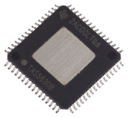
Product Sample & Technical Tools & Support & Folder Buy Documents Software Community TAS5630B SLES217D–NOVEMBER2010–REVISEDMARCH2015 TAS5630B 300-W Stereo and 400-W Mono PurePath™ HD Analog-Input Power Stage 1 Features 3 Description • PurePath™HDEnabledIntegratedFeedback The TAS5630B device is a high-performance analog- 1 input class-D amplifier with integrated closed-loop Provides: feedback technology (known as PurePath HD – SignalBandwidthupto80kHzforHigh- technology) with the ability to drive up to 300 W (1) FrequencyContentFromHDSources stereo into 4-Ω to 8-Ω speakers from a single 50-V – Ultralow0.03%THDat1Winto4 Ω supply. – FlatTHDatAllFrequenciesforNaturalSound PurePath HD technology enables traditional AB- – 80-dBPSRR(BTL,NoInputSignal) amplifier performance (< 0.03% THD) levels while providing the power efficiency of traditional class-D – > 100-dB(A-weighted)SNR amplifiers. – Click-andPop-FreeStart-up Unlike traditional class-D amplifiers, the distortion • MultipleConfigurationsPossibleontheSame curve does not increase until the output levels move PCBWithStuffingOptions: intoclipping. – MonoParallelBridge-TiedLoad(PBTL) PurePath HD technology enables lower idle losses, – StereoBridge-TiedLoad(BTL) making the device even more efficient. When coupled – 2.1Single-EndedStereoPairandBTL with TI’s class-G power-supply reference design for Subwoofer TAS563x, industry-leading levels of efficiency can be achieved. – QuadSingle-EndedOutputs • TotalOutputPowerat10%THD+N DeviceInformation(1) – 400WinMonoPBTLConfiguration PARTNUMBER PACKAGE BODYSIZE(NOM) – 300WperChannelinStereoBTL HSSOP(44) 15.90mm×11.00mm TAS5630B Configuration HTQFP(64) 14.00mm×14.00mm – 145WperChannelinQuadSingle-Ended (1) For all available packages, see the orderable addendum at Configuration theendofthedatasheet. • High-EfficiencyPowerStage(> 88%)With60-mΩ TypicalTAS5630BApplicationBlockDiagram OutputMOSFETs • TwoThermallyEnhancedPackageOptions: 3´OPA1632 ♫♪ – PHD(64-PinQFP) – DKD(44-PinPSOP3) ANALOG PurePathTMHD ♫♪ AUDIO TAS5630B • Self-ProtectionDesign(IncludingUndervoltage, INPUT (2.1 Configuration) Overtemperature,Clipping,andShort-Circuit ♫♪ Protection)WithErrorReporting ±15 V 12V 25V–50 V • EMICompliantWhenUsedWithRecommended SystemDesign PurePathTMHD Class-G Power Supply Ref. Design 2 Applications • MiniComboSystem 110VAC®240 VAC • AVReceivers (1) Achievableoutputpowerlevelsaredependentonthethermal • DVDReceivers configurationofthetargetapplication.Ahigh-performance thermalinterfacematerialbetweentheexposedpackageheat • ActiveSpeakers slugandtheheatsinkshouldbeusedtoachievehighoutput powerlevels. 1 An IMPORTANT NOTICE at the end of this data sheet addresses availability, warranty, changes, use in safety-critical applications, intellectualpropertymattersandotherimportantdisclaimers.PRODUCTIONDATA.
TAS5630B SLES217D–NOVEMBER2010–REVISEDMARCH2015 www.ti.com Table of Contents 1 Features.................................................................. 1 7.1 Overview.................................................................14 2 Applications........................................................... 1 7.2 FunctionalBlockDiagram.......................................14 3 Description............................................................. 1 7.3 FeatureDescription.................................................15 7.4 DeviceFunctionalModes........................................18 4 RevisionHistory..................................................... 2 8 ApplicationandImplementation........................ 19 5 PinConfigurationandFunctions......................... 4 8.1 ApplicationInformation............................................19 6 Specifications......................................................... 7 8.2 TypicalApplication..................................................20 6.1 AbsoluteMaximumRatings......................................7 9 PowerSupplyRecommendations...................... 27 6.2 ESDRatings..............................................................7 10 Layout................................................................... 27 6.3 RecommendedOperatingConditions.......................7 6.4 ThermalInformation..................................................8 10.1 LayoutGuidelines.................................................27 6.5 ElectricalCharacteristics...........................................8 10.2 LayoutExample....................................................28 6.6 AudioCharacteristics(BTL)....................................10 11 DeviceandDocumentationSupport................. 30 6.7 AudioSpecification(Single-EndedOutput)............10 11.1 Trademarks...........................................................30 6.8 AudioSpecification(PBTL) ....................................11 11.2 ElectrostaticDischargeCaution............................30 6.9 TypicalCharacteristics............................................11 11.3 Glossary................................................................30 7 DetailedDescription............................................ 14 12 Mechanical,Packaging,andOrderable Information........................................................... 30 4 Revision History ChangesfromRevisionC(September2012)toRevisionD Page • AddedPinConfigurationandFunctionssection,ESDRatingstable,FeatureDescriptionsection,DeviceFunctional Modes,ApplicationandImplementationsection,PowerSupplyRecommendationssection,Layoutsection,Device andDocumentationSupportsection,andMechanical,Packaging,andOrderableInformationsection .............................. 1 • ChangedThermalInformationtabledata............................................................................................................................... 8 ChangesfromRevisionB(November2011)toRevisionC Page • ChangedAnalogcomparatorreferencenode,VI_CMVlauesFrom:MIN=1.5TYP=1.75MAX=1.9To:MIN= 1.75TYP=2MAX=2.15...................................................................................................................................................... 8 • ChangedANALOGINPUTS-V TYPvalueFrom3.5to5V ............................................................................................ 8 IN PP • ChangedtheV andV TestConditionsFrom:INPUT_X,M1,M2,M3,RESETTo:M1,M2,M3,RESET........................ 9 IH IL • Deleted-R =2Ω,1%THD+N,unclippedoutputsignalFromP intheAudioSpecification(PBTL)table.......................11 L O ChangesfromRevisionA(November2011)toRevisionB Page • ChangedtheR parametersfrom/OTW1toVREG,/OTW2toVREG,/SDtoVREGto/OTW,/OTW1,/OTW2, INT_PU /CLIP,READY,/SDtoVRE.................................................................................................................................................... 9 • AddedtexttothePHDPackagesection.............................................................................................................................. 17 • AddedtexttotheDKDPackagesection.............................................................................................................................. 17 ChangesfromOriginal(November2010)toRevisionA Page • ChangedTitleFrom:600-WMONOTo:400-WMONO......................................................................................................... 1 • ChangedFeatureFrom:600WperChannelinMonoPBTLConfigurationTo:400WperChannelinMonoPBTL Configuration.......................................................................................................................................................................... 1 • ChangedthePinOneLocationPackageimage.................................................................................................................... 5 • ChangedR (PBTL)LoadImpedanceMinvalueFrom:1.6ΩTo:2.4Ω,andTypvalueFrom2To:3Ω............................. 7 L • AddedfootnotestotheROCtable......................................................................................................................................... 7 • AddedR informationtotheROCTable............................................................................................................................ 8 OCP 2 SubmitDocumentationFeedback Copyright©2010–2015,TexasInstrumentsIncorporated ProductFolderLinks:TAS5630B
TAS5630B www.ti.com SLES217D–NOVEMBER2010–REVISEDMARCH2015 • ChangedtheI TypicalValueFrom:19ATo:15A............................................................................................................. 9 OC • Deleted-R =2Ω,10%,THD+N,clippedinputsignalFromP intheAudioSpecification(PBTL)table.......................... 11 L O • ReplacedtheTYPICALCHARACTERISTICS,PBTLCONFIGURATIONgraphs............................................................... 12 • Addedsection-ClickandPopinSE-Mode......................................................................................................................... 18 • Addedsection-PBTLOverloadandShortCircuit............................................................................................................... 18 • ReplacedthePACKAGEHEATDISSIPATIONRATINGStablewiththeTHERMALINFORMATIONtable....................... 18 Copyright©2010–2015,TexasInstrumentsIncorporated SubmitDocumentationFeedback 3 ProductFolderLinks:TAS5630B
TAS5630B SLES217D–NOVEMBER2010–REVISEDMARCH2015 www.ti.com 5 Pin Configuration and Functions DKDPackage 44PinsHSSOP TopView PSU_REF 1 44 GVDD_AB VDD 2 43 BST_A OC_ADJ 3 42 PVDD_A RESET 4 41 PVDD_A C_STARTUP 5 40 OUT_A INPUT_A 6 39 OUT_A INPUT_B 7 38 GND_A VI_CM 8 37 GND_B GND 9 4 36 OUT_B 4 AVGRNEGD 1110 (TOPpinsP 3354 BPSVTD_DB_B INPUT_C 12 VA 33 BST_C INPUT_D 13 IEWCK 32 PVDD_C FREQ_ADJ 14 )AG 31 OUT_C E OSC_IO+ 15 30 GND_C OSC_IO- 16 29 GND_D SD 17 28 OUT_D OTW 18 27 OUT_D READY 19 26 PVDD_D M1 20 25 PVDD_D M2 21 24 BST_D M3 22 23 GVDD_CD PHDPackage 64PinsHTQFP TopView VDDPSU_REFNCNCNCNCGNDGNDGVDD_BGVDD_ABST_AOUT_AOUT_APVDD_APVDD_AGND_A 4321098765432109 OC_ADJ 1666665555555555448 GND_A RESET 2 47 GND_B C_STARTUP 3 46 GND_B INPUT_A 4 45 OUT_B INPUT_B 5 44 OUT_B VI_CM 6 43 PVDD_B GND 7 42 PVDD_B AGND 8 41 BST_B VREG 9 40 BST_C INPUT_C 10 39 PVDD_C INPUT_D 11 38 PVDD_C FREQ_ADJ 12 37 OUT_C OSC_IO+ 13 36 OUT_C OSC_IO- 14 35 GND_C SD 15 64-pins QFPpackage 34 GND_C OTW1 16 33 GND_D 17181920212223242526272829303132 OTW2CLIPREADYM1M2M3GNDGNDVDD_CVDD_DBST_DOUT_DOUT_DVDD_DVDD_DGND_D GG PP 4 SubmitDocumentationFeedback Copyright©2010–2015,TexasInstrumentsIncorporated ProductFolderLinks:TAS5630B
TAS5630B www.ti.com SLES217D–NOVEMBER2010–REVISEDMARCH2015 Electrical Pin 1 Pin 1 Marker White Dot Figure1. PinOneLocationPHDPackage PinFunctions PIN FUNCTION(1) DESCRIPTION NAME HTQFP HSSOP AGND 8 10 P Analogground BST_A 54 43 P HSbootstrapsupply(BST),external0.033-μFcapacitortoOUT_Arequired. BST_B 41 34 P HSbootstrapsupply(BST),external0.033-μFcapacitortoOUT_Brequired. BST_C 40 33 P HSbootstrapsupply(BST),external0.033-μFcapacitortoOUT_Crequired. BST_D 27 24 P HSbootstrapsupply(BST),external0.033-μFcapacitortoOUT_Drequired. CLIP 18 — O Clippingwarning;opendrain;active-low C_STARTUP 3 5 O Start-upramprequiresachargingcapacitorof4.7nFtoAGNDinBTLmode FREQ_ADJ 12 14 I PWMframe-rate-programmingpinrequiresresistortoAGND 7,23,24,57, GND 9 P Ground 58 GND_A 48,49 38 P Powergroundforhalf-bridgeA GND_B 46,47 37 P Powergroundforhalf-bridgeB GND_C 34,35 30 P Powergroundforhalf-bridgeC GND_D 32,33 29 P Powergroundforhalf-bridgeD GVDD_A 55 — P Gate-drivevoltagesupplyrequires0.1-μFcapacitortoGND_A GVDD_B 56 — P Gatedrivevoltagesupplyrequires0.1-μFcapacitortoGND_B GVDD_C 25 — P Gatedrivevoltagesupplyrequires0.1-μFcapacitortoGND_C GVDD_D 26 — P Gatedrivevoltagesupplyrequires0.1-μFcapacitortoGND_D GVDD_AB — 44 P Gatedrivevoltagesupplyrequires0.22-μFcapacitortoGND_A/GND_B GVDD_CD — 23 P Gatedrivevoltagesupplyrequires0.22-μFcapacitortoGND_C/GND_D INPUT_A 4 6 I Inputsignalforhalf-bridgeA INPUT_B 5 7 I Inputsignalforhalf-bridgeB INPUT_C 10 12 I Inputsignalforhalf-bridgeC INPUT_D 11 13 I Inputsignalforhalf-bridgeD M1 20 20 I Modeselection M2 21 21 I Modeselection M3 22 22 I Modeselection NC 59–62 – — Noconnect;pinsmaybegrounded. (1) I=Input,O=Output,P=Power Copyright©2010–2015,TexasInstrumentsIncorporated SubmitDocumentationFeedback 5 ProductFolderLinks:TAS5630B
TAS5630B SLES217D–NOVEMBER2010–REVISEDMARCH2015 www.ti.com PinFunctions(continued) PIN FUNCTION(1) DESCRIPTION NAME HTQFP HSSOP Analogovercurrent-programmingpinrequiresresistortoAGND.64-pin OC_ADJ 1 3 O package(PHD)=22kΩ.44-pinPSOP3(DKD)=24kΩ OSC_IO+ 13 15 I/O Oscillatormaster/slaveoutput/input OSC_IO– 14 16 I/O Oscillatormaster/slaveoutput/input OTW — 18 O Overtemperaturewarningsignal,open-drain,active-low OTW1 16 — O Overtemperaturewarningsignal,open-drain,active-low OTW2 17 — O Overtemperaturewarningsignal,open-drain,active-low OUT_A 52,53 39,40 O Output,half-bridgeA OUT_B 44,45 36 O Output,half-bridgeB OUT_C 36,37 31 O Output,half-bridgeC OUT_D 28,29 27,28 O Output,half-bridgeD PSU_REF 63 1 P PSUreferencerequiresclosedecouplingof330pFtoAGND. Power-supplyinputforhalf-bridgeArequiresclosedecouplingof0.01-μF PVDD_A 50,51 41,42 P capacitorinparallelwith2.2-μFcapacitortoGND_A. Power-supplyinputforhalf-bridgeBrequiresclosedecouplingof0.01-μF PVDD_B 42,43 35 P capacitorinparallelwith2.2-μFcapacitortoGND_B. Power-supplyinputforhalf-bridgeCrequiresclosedecouplingof0.0-μF PVDD_C 38,39 32 P capacitorinparallelwith2.2-μFcapacitortoGND_C. Power-supplyinputforhalf-bridgeDrequiresclosedecouplingof0.01-μF PVDD_D 30,31 25,26 P capacitorinparallelwith2.2-μFcapacitortoGND_D. READY 19 19 O Normaloperation;open-drain;active-high RESET 2 4 I Deviceresetinput;active-low SD 15 17 O Shutdownsignal,open-drain,active-low Powersupplyfordigitalvoltageregulatorrequiresa10-μFcapacitorinparallel VDD 64 2 P witha0.1-μFcapacitortoGNDfordecoupling. Analogcomparatorreferencenoderequiresclosedecouplingof1nFto VI_CM 6 8 O AGND. VREG 9 11 P Regulatorsupplyfilterpinrequires0.1-μFcapacitortoAGND. 6 SubmitDocumentationFeedback Copyright©2010–2015,TexasInstrumentsIncorporated ProductFolderLinks:TAS5630B
TAS5630B www.ti.com SLES217D–NOVEMBER2010–REVISEDMARCH2015 6 Specifications 6.1 Absolute Maximum Ratings overoperatingfree-airtemperaturerangeunlessotherwisenoted (1) MIN MAX UNIT VDDtoAGND –0.3 13.2 V GVDDtoAGND –0.3 13.2 V PVDD_XtoGND_X(2) –0.3 69 V OUT_XtoGND_X(2) –0.3 69 V BST_XtoGND_X(2) –0.3 82.2 V BST_XtoGVDD_X(2) –0.3 69 V VREGtoAGND –0.3 4.2 V GND_XtoGND –0.3 0.3 V GND_XtoAGND –0.3 0.3 V OC_ADJ,M1,M2,M3,OSC_IO+,OSC_IO–,FREQ_ADJ,VI_CM,C_STARTUP,PSU_REFtoAGND –0.3 4.2 V INPUT_X –0.3 7 V RESET,SD,OTW1,OTW2,CLIP,READYtoAGND –0.3 7 V Continuoussinkcurrent(SD,OTW1,OTW2,CLIP,READY) 9 mA Operatingjunctiontemperature,TJ 0 150 °C Storagetemperature,Tstg –40 150 °C (1) StressesbeyondthoselistedunderAbsoluteMaximumRatingsmaycausepermanentdamagetothedevice.Thesearestressratings only,andfunctionaloperationofthedeviceattheseoranyotherconditionsbeyondthoseindicatedunderRecommendedOperating Conditionsisnotimplied.Exposuretoabsolute-maximum-ratedconditionsforextendedperiodsmayaffectdevicereliability. (2) Thesevoltagesrepresentsthedcvoltage+peakacwaveformmeasuredattheterminalofthedeviceinallconditions. 6.2 ESD Ratings VALUE UNIT Humanbodymodel(HBM),perANSI/ESDA/JEDECJS-001(1) ±2000 V(ESD) Electrostaticdischarge Charged-devicemodel(CDM),perJEDECspecificationJESD22- ±500 V C101(2) (1) JEDECdocumentJEP155statesthat500-VHBMallowssafemanufacturingwithastandardESDcontrolprocess. (2) JEDECdocumentJEP157statesthat250-VCDMallowssafemanufacturingwithastandardESDcontrolprocess. 6.3 Recommended Operating Conditions overoperatingfree-airtemperaturerange(unlessotherwisenoted) MIN NOM MAX UNIT PVDD_x Half-bridgesupply DCsupplyvoltage 25 50 52.5 V GVDD_x Supplyforlogicregulatorsandgate-drivecircuitry DCsupplyvoltage 10.8 12 13.2 V VDD Digitalregulatorsupplyvoltage DCsupplyvoltage 10.8 12 13.2 V RL(BTL) 3.5 4 RL(SE)(2) Loadimpedance(1) Oapuptplicuattfiioltnerinafcocrmoradtiinogntsoescctihoenmaticsinthe 1.8 2 Ω RL(PBTL)(2) 2.4 3 LOUTPUT(BTL) 7 10 LOUTPUT(SE)(2) Outputfilterinductance(1) MinimumoutputinductanceatIOC 7 15 μH LOUTPUT(PBTL)(2) 7 10 Nominal 385 400 415 PWMframerateselectableforAMinterference fPWM avoidance;1%resistortolerance. AM1 315 333 350 kHz AM2 260 300 335 Nominal;mastermode 9.9 10 10.1 RFREQ_ADJ PWMframe-rate-programmingresistor AM1;mastermode 19.8 20 20.2 kΩ AM2;mastermode 29.7 30 30.3 (1) Valuesareforactualmeasuredimpedanceoverallcombinationsoftolerance,currentandtemperatureandnotsimplythecomponent rating. (2) SeeadditionaldetailsforSEandPBTLinSystemDesignConsiderations. Copyright©2010–2015,TexasInstrumentsIncorporated SubmitDocumentationFeedback 7 ProductFolderLinks:TAS5630B
TAS5630B SLES217D–NOVEMBER2010–REVISEDMARCH2015 www.ti.com Recommended Operating Conditions (continued) overoperatingfree-airtemperaturerange(unlessotherwisenoted) MIN NOM MAX UNIT VoltageonFREQ_ADJpinforslavemode VFREQ_ADJ operation Slavemode 3.3 V Overcurrent-protection-programmingresistor, 64-pinQFPpackage(PHD) 22 33 cycle-by-cyclemode 44-PinPSOP3package(DKD) 24 33 ROCP kΩ Overcurrent-protection-programmingresistor, PHDorDKD 47 68 latchingmode TJ Junctiontemperature 0 125 °C 6.4 Thermal Information TAS5630B THERMALMETRIC(1) PHD(HTQFP) DKD(HSSOP) UNIT 64PINS 44PINS R Junction-to-ambientthermalresistance 8.6 8.8 θJA R Junction-to-case(top)thermalresistance 0.3 0.4 θJC(top) R Junction-to-boardthermalresistance 2.1 3.0 °C/W θJB ψ Junction-to-topcharacterizationparameter 0.4 0.4 JT ψ Junction-to-boardcharacterizationparameter 2.1 3.0 JB (1) Formoreinformationabouttraditionalandnewthermalmetrics,seetheICPackageThermalMetricsapplicationreport(SPRA953). 6.5 Electrical Characteristics PVDD_X=50V,GVDD_X=12V,VDD=12V,T (Casetemperature)=75°C,f =400kHz,unlessotherwisespecified. C S PARAMETER TESTCONDITIONS MIN TYP MAX UNIT INTERNALVOLTAGEREGULATORANDCURRENTCONSUMPTION Voltageregulator,onlyusedasreference VREG VDD=12V 3 3.3 3.6 V node,VREG VI_CM Analogcomparatorreferencenode,VI_CM 1.75 2 2.15 V Operating,50%dutycycle 22.5 I VDDsupplycurrent mA VDD Idle,resetmode 22.5 50%dutycycle 12.5 I GVDD_xgate-supplycurrentperhalf-bridge mA GVDD_X Resetmode 1.5 50%dutycyclewithrecommendedoutput 13.3 mA I Half-bridgesupplycurrent filter PVDD_X Resetmode,Noswitching 870 μA ANALOGINPUTS R Inputresistance READY=HIGH 33 kΩ IN Maximuminputvoltagewithsymmetrical V 5 V IN outputswing PP I Maximuminputcurrent 342 μA IN G Voltagegain(V /V ) 23 dB OUT IN OSCILLATOR Nominal,mastermode 3.85 4 4.15 f AM1,mastermode F ×10 3.15 3.33 3.5 MHz OSC_IO+ PWM AM2,mastermode 2.6 3 3.35 V Highlevelinputvoltage 1.86 V IH V Lowlevelinputvoltage 1.45 V IL 8 SubmitDocumentationFeedback Copyright©2010–2015,TexasInstrumentsIncorporated ProductFolderLinks:TAS5630B
TAS5630B www.ti.com SLES217D–NOVEMBER2010–REVISEDMARCH2015 Electrical Characteristics (continued) PVDD_X=50V,GVDD_X=12V,VDD=12V,T (Casetemperature)=75°C,f =400kHz,unlessotherwisespecified. C S PARAMETER TESTCONDITIONS MIN TYP MAX UNIT OUTPUT-STAGEMOSFETs Drain-to-sourceresistance,lowside(LS) T =25°C,excludesmetallization 60 100 R J mΩ DS(on) Drain-to-sourceresistance,highside(HS) resistance,GVDD=12V 60 100 I/OPROTECTION Undervoltageprotectionlimit,GVDD_xand V 9.5 V uvp,G VDD V (1) 0.6 V uvp,hyst OTW1(1) Overtemperaturewarning1 95 100 105 °C OTW2(1) Overtemperaturewarning2 115 125 135 °C TemperaturedropneededbelowOTW OTW (1) temperatureforOTWtobeinactiveafter 25 °C hyst OTWevent Overtemperatureerror 145 155 165 °C OTE(1) OTE-OTWdifferential 30 OTE (1) AresetmustoccurforSDtobereleased 25 °C hyst followinganOTEevent. OLPC Overloadprotectioncounter f =400kHz 2.6 ms PWM Resistor–programmable,nominalpeak currentin1-Ωload, 15 64-pinQFPpackage(PHD) R =22kΩ Overcurrentlimitprotection OCP Resistor–programmable,nominalpeak I currentin1-Ωload, A OC 15 44-pinPSOP3package(DKD), R =24kΩ OCP Resistor–programmable,nominalpeak Overcurrentlimitprotection,latched currentin1-Ωload, 15 R =47kΩ OCP Timefromswitchingtransitiontoflip-state I Overcurrentresponsetime 150 ns OCT inducedbyovercurrent ConnectedwhenRESETisactiveto Internalpulldownresistoratoutputofeach I providebootstrapcharge.NotusedinSE 3 mA PD half-bridge mode STATICDIGITALSPECIFICATIONS V High-levelinputvoltage 2 V IH M1,M2,M3,RESET V Low-levelinputvoltage 0.8 V IL I Inputleakagecurrent 100 μA lkg OTW/SHUTDOWN(SD) Internalpullupresistance,OTW,OTW1, R 20 26 32 kΩ INT_PU OTW2,CLIP,READY,SDtoVREG Internalpullupresistor 3 3.3 3.6 V High-leveloutputvoltage V OH Externalpullupof4.7kΩto5V 4.5 5 V Low-leveloutputvoltage I =4mA 200 500 mV OL O DevicefanoutOTW,OTW1,OTW2,SD, FANOUT Noexternalpullup 30 devices CLIP,READY (1) Specifiedbydesign. Copyright©2010–2015,TexasInstrumentsIncorporated SubmitDocumentationFeedback 9 ProductFolderLinks:TAS5630B
TAS5630B SLES217D–NOVEMBER2010–REVISEDMARCH2015 www.ti.com 6.6 Audio Characteristics (BTL) PCBandsystemconfigurationareinaccordancewithrecommendedguidelines.Audiofrequency=1kHz,PVDD_X=50V, GVDD_X=12V,R =4Ω,f =400kHz,R =22kΩ,T =75°C;outputfilter:L =7μH,C =680nF, L S OC C DEM DEM MODE=010,unlessotherwisenoted. PARAMETER TESTCONDITIONS MIN TYP MAX UNIT R =4Ω,10%THD+N,clippedoutputsignal 300 L R =6Ω,10%THD+N,clippedoutputsignal 210 L R =8Ω,10%THD+N,clippedoutputsignal 160 L P Poweroutputperchannel W O R =4Ω,1%THD+N,unclippedoutputsignal 240 L R =6Ω,1%THD+N,unclippedoutputsignal 160 L R =8Ω,1%THD+N,unclippedoutputsignal 125 L THD+N Totalharmonicdistortion+noise 1W 0.03% A-weighted,AES17filter,inputcapacitor V Outputintegratednoise 270 μV n grounded |V | Outputoffsetvoltage Inputsac-coupledtoAGND 20 50 mV OS SNR Signal-to-noiseratio(1) A-weighted,AES17filter 100 dB DNR Dynamicrange A-weighted,AES17filter 100 dB P Powerdissipationduetoidlelosses(I ) P =0,fourchannelsswitching(2) 2.7 W idle PVDD_X O (1) SNRiscalculatedrelativeto1%THD+Noutputlevel. (2) Actualsystemidlelossesalsoareaffectedbycorelossesofoutputinductors. 6.7 Audio Specification (Single-Ended Output) PCBandsystemconfigurationareinaccordancewithrecommendedguidelines.Audiofrequency=1kHz,PVDD_X=50V, GVDD_X=12V,R =4Ω,f =400kHz,R =22kΩ,T =75°C;outputfilter:L =15μH,C =470μF, L S OC C DEM DEM MODE=100,unlessotherwisenoted. PARAMETER TESTCONDITIONS MIN TYP MAX UNIT R =2Ω,10%THD+N,clippedoutputsignal 145 L R =3Ω,10%THD+N,clippedoutputsignal 100 L R =4Ω,10%THD+N,clippedoutputsignal 75 L P Poweroutputperchannel W O R =2Ω,1%THD+N,unclippedoutputsignal 110 L R =3Ω,1%THD+N,unclippedoutputsignal 75 L R =4Ω,1%THD+N,unclippedoutputsignal 55 L THD+N Totalharmonicdistortion+noise 1W 0.07% V Outputintegratednoise A-weighted,AES17filter,inputcapacitorgrounded 340 μV n SNR Signal-to-noiseratio(1) A-weighted,AES17filter 93 dB DNR Dynamicrange A-weighted,AES17filter 93 dB P Powerdissipationduetoidlelosses P =0,fourchannelsswitching(2) 2 W idle (I ) O PVDD_X (1) SNRiscalculatedrelativeto1%THD+Noutputlevel. (2) Actualsystemidlelossesareaffectedbycorelossesofoutputinductors. 10 SubmitDocumentationFeedback Copyright©2010–2015,TexasInstrumentsIncorporated ProductFolderLinks:TAS5630B
TAS5630B www.ti.com SLES217D–NOVEMBER2010–REVISEDMARCH2015 6.8 Audio Specification (PBTL) PCBandsystemconfigurationareinaccordancewithrecommendedguidelines.Audiofrequency=1kHz,PVDD_X=50V, GVDD_X=12V,R =3Ω,f =400kHz,R =22kΩ,T =75°C;outputfilter:L =7μH,C =1.5μF, L S OC C DEM DEM MODE=101-10,unlessotherwisenoted. PARAMETER TESTCONDITIONS MIN TYP MAX UNIT R =3Ω,10%THD+N,clippedoutputsignal 400 L R =4Ω,10%THD+N,clippedoutputsignal 300 L P Poweroutputperchannel W O R =3Ω,1%THD+N,unclippedoutputsignal 310 L R =4Ω,1%THD+N,unclippedoutputsignal 230 L THD+N Totalharmonicdistortion+noise 1W 0.05% V Outputintegratednoise A-weighted 260 μV n SNR Signaltonoiseratio(1) A-weighted 100 dB DNR Dynamicrange A-weighted 100 dB P Powerdissipationduetoidlelosses(IPVDD_X) P =0,fourchannelsswitching(2) 2.7 W idle O (1) SNRiscalculatedrelativeto1%THD-Noutputlevel. (2) Actualsystemidlelossesareaffectedbycorelossesofoutputinductors. 6.9 Typical Characteristics 6.9.1 BTLConfiguration 10 340 46WW 320 46WW Noise − % 8W 223680000 8W N − Total Harmonic Distortion + 0.11 P − Output Power − WO11111222802468024000000000 D+ 60 TH0.01 TC = 75(cid:176)C 2400 TTCH D= +7N5 (cid:176)aCt 10% 0.005 0 20m 100m 1 10 100 400 25 30 35 40 45 50 PO − Output Power − W G001 PVDD − Supply Voltage − V G001 Figure2.TotalHarmonic+NoisevsOutputPower Figure3.OutputPowervsSupplyVoltage 300 100 280 46WW 9905 260 8W 85 240 80 220 75 P − Output Power − WO111112024680000000 Efficiency − % 334455667050505050 80 25 60 20 40 15 4W 20 TC = 75(cid:176)C 150 68WW TTCH D= +2N5 (cid:176)aCt 10% 0 0 25 30 35 40 45 50 0 100 200 300 400 500 600 700 PVDD − Supply Voltage − V 2 Channel Output Power − W G001 G001 Figure4.UnclippedOutputPowervsSupplyVoltage Figure5.SystemEfficiencyvsOutputPower Copyright©2010–2015,TexasInstrumentsIncorporated SubmitDocumentationFeedback 11 ProductFolderLinks:TAS5630B
TAS5630B SLES217D–NOVEMBER2010–REVISEDMARCH2015 www.ti.com BTL Configuration (continued) 100 340 899505 468WWW 330200 280 80 75 260 70 W 240 Power Loss − W 3344556605050505 P − Output Power − O 111112202468020000000 25 80 20 60 11505 TTCH D= +2N5 (cid:176)aCt 10% 2400 468WWW THD+N at 10% 0 0 0 100 200 300 400 500 600 700 −10 0 10 20 30 40 50 60 70 80 90 100110 2 Channel Output Power − W G001 TC − Case Temperature − (cid:176)C G001 Figure6.SystemPowerLossvsOutputPower Figure7.OutputPowervsCaseTemperature 0 −10 TC = 75(cid:176)C 4W VREF = 35.36 V −20 Sample Rate = 48kHz −30 FFT Size = 16384 −40 −50 B mplitude − d −−−876000 A −90 Noise −−111000 −120 −130 −140 −150 −160 0 2k 4k 6k 8k 10k 12k 14k 16k 18k 20k 22k f − Frequency − Hz G001 Figure8.NoiseAmplitudevsFrequency 6.9.2 SEConfiguration 1ChannelDriven 10 170 23WW 160 23WW Noise − % 4W 111345000 4W N − Total Harmonic Distortion + 0.11 P − Output Power − WO111456789012000000000 D+ 30 TH0.01 TC = 75(cid:176)C 1200 TTCH D= +7N5 (cid:176)aCt 10% 0.005 0 20m 100m 1 10 100200 25 30 35 40 45 50 PO − Output Power − W G001 PVDD − Supply Voltage − V G001 Figure9.TotalHarmonicDistortion+NoisevsOutput Figure10.OutputPowervsSupplyVoltage Power 12 SubmitDocumentationFeedback Copyright©2010–2015,TexasInstrumentsIncorporated ProductFolderLinks:TAS5630B
TAS5630B www.ti.com SLES217D–NOVEMBER2010–REVISEDMARCH2015 SE Configuration (continued) 180 170 160 150 140 130 Power − W 111012000 P − Output O 67890000 50 40 30 20 23WW 10 4W THD+N at 10% 0 −10 0 10 20 30 40 50 60 70 80 90 100110 TC − Case Temperature − (cid:176)C G001 Figure11.OutputPowervsCaseTemperature 6.9.3 PBTLConfiguration 10 500 3W 3W Noise − % 468WWW 440500 468WWW D+N − Total Harmonic Distortion + 0.11 P − Output Power − WO112233050505000000 H T0.01 TC = 75(cid:176)C 50 TTCH D= +7N5 (cid:176)aCt 10% 0.005 0 20m 100m 1 10 100 700 25 30 35 40 45 50 PO − Output Power − W G001 PVDD − Supply Voltage − V G001 Figure12.TotalHarmonicDistortion+NoisevsOutput Figure13.OutputPowervsSupplyVoltage Power 500 450 400 W 350 wer − 300 Po P − Output O 122505000 100 3W 4W 50 6W 8W THD+N at 10% 0 −10 0 10 20 30 40 50 60 70 80 90 100110 TC − Case Temperature − (cid:176)C G001 Figure14.OutputPowervsCaseTemperature Copyright©2010–2015,TexasInstrumentsIncorporated SubmitDocumentationFeedback 13 ProductFolderLinks:TAS5630B
TAS5630B SLES217D–NOVEMBER2010–REVISEDMARCH2015 www.ti.com 7 Detailed Description 7.1 Overview TAS5630Bisananaloginput,audioPWM(class-D)amplifier.TheoutputoftheTAS5630Bcanbeconfiguredfor single-ended, bridge-tied load (BTL) or parallel BTL (PBTL) output. It requires two rails for power supply, PVDD and 12 V (GVDD and VDD). The following functional block diagram shows interconnections of internal supplies, control logic, gate drives and power amplifiers. Detailed schematic can be viewed in TAS5630B EVM User's Guide(SLAU287). 7.2 Functional Block Diagram /CLIP READY /OTW1 /OTW2 /SD MM12 LOGIC VDD M3 &I/O CTION PORWEESRE-TUP UVP VREG VREG /RESET PROTE TEMP GVDD_A GVDD_C AGND C_STARTUP CSOTANRTTRUOPL SENSE GVDD_B GVDD_D GND PORVOETRE-CLOTIAODN CB3C CUSERNRSEENT OC_ADJ OSC_SYNC_IO+ OSC_SYNC_IO- OSCILLATOR 4 PVDD_X PPSC 4 OUT_X FREQ_ADJ 4 GND_X GVDD_A PWM ACTIVITY BST_A DETECTOR PSU_REF 4 PVDD_X PVDD_A PSU_FF VI_CM GND REPCWEIMVER CONTROL COTINMTINRGOL GATE-DRIVE OUT_A GND_A GVDD_B - ANALOG + BST_B INPUT_A LOOPFILTER PVDD_B + ANALOG - REPCWEIMVER CONTROL COTINMTINRGOL GATE-DRIVE OUT_B INPUT_B LOOPFILTER MUX GND_B INPUT_C LOAONPAFLIOLTGER ANALOGINPUTMUX +- ANALOGCOMPARATOR REPCWEIMVER CONTROL COTINMTINRGOL GATE-DRIVE GOPBVSVUDTDT_D_DCC__CC + INPUT_D ANALOG - GND_C LOOPFILTER GVDD_D BST_D PVDD_D REPCWEIMVER CONTROL COTINMTINRGOL GATE-DRIVE OUT_D GND_D 14 SubmitDocumentationFeedback Copyright©2010–2015,TexasInstrumentsIncorporated ProductFolderLinks:TAS5630B
TAS5630B www.ti.com SLES217D–NOVEMBER2010–REVISEDMARCH2015 7.3 Feature Description 7.3.1 PowerSupplies Tofacilitatesystemdesign,theTAS5630Bneedsonlya12-Vsupplyinadditiontothe(typical)50-Vpower-stage supply. An internal voltage regulator provides suitable voltage levels for the digital and low-voltage analog circuitry. Additionally, all circuitry requiring a floating voltage supply, for example, the high-side gate drive, is accommodatedbybuilt-inbootstrapcircuitryrequiringonlyanexternalcapacitorforeachhalf-bridge. To provide outstanding electrical and acoustical characteristics, the PWM signal path, including gate drive and output stage, is designed as identical, independent half-bridges. For this reason, each half-bridge has separate gate drive supply pins (GVDD_X), bootstrap pins (BST_X), and power-stage supply pins (PVDD_X). Furthermore, an additional pin (VDD) is provided as supply for all common circuits. Although supplied from the same 12-V source, it is highly recommended to separate GVDD_A, GVDD_B, GVDD_C, GVDD_D, and VDD on the printed-circuit board (PCB) by RC filters (see Typical Application for details). These RC filters provide the recommended high-frequency isolation. Special attention should be paid to placing all decoupling capacitors as close to their associated pins as possible. In general, inductance between the power supply pins and decoupling capacitorsmustbeavoided.(SeeSLAU287foradditionalinformation.) Foraproperlyfunctioningbootstrapcircuit,asmallceramiccapacitormustbeconnectedfromeachbootstrappin (BST_X) to the power-stage output pin (OUT_X). When the power-stage output is low, the bootstrap capacitor is charged through an internal diode connected between the gate-drive power-supply pin (GVDD_X) and the bootstrap pin. When the power-stage output is high, the bootstrap capacitor potential is shifted above the output potential and thus provides a suitable voltage supply for the high-side gate driver. In an application with PWM switchingfrequenciesintherangefrom300kHzto400kHz,itisrecommendedtouse33-nFceramiccapacitors, size 0603 or 0805, for the bootstrap supply. These 33-nF capacitors ensure sufficient energy storage, even during minimal PWM duty cycles, to keep the high-side power stage FET (LDMOS) fully turned on during the remainingpartofthePWMcycle. Special attention should be paid to the power-stage power supply; this includes component selection, PCB placement, and routing. As indicated, each half-bridge has independent power-stage supply pins (PVDD_X). For optimal electrical performance, EMI compliance, and system reliability, it is important that each PVDD_X pin is decoupled with a 2.2-μF ceramic capacitor placed as close as possible to each supply pin. It is recommended to follow the PCB layout of the TAS5630B reference design. For additional information on recommended power supplyandrequiredcomponents,seeTypicalApplication. The 12-V supply should be from a low-noise, low-output-impedance voltage regulator. Likewise, the 50-V power- stage supply is assumed to have low output impedance and low noise. The power-supply sequence is not critical as facilitated by the internal power-on-reset circuit. Moreover, the TAS5630B is fully protected against erroneous power-stage turnon due to parasitic gate charging. Thus, voltage-supply ramp rates (dV/dt) are non-critical within thespecifiedrange(seeRecommendedOperatingConditions). 7.3.2 SystemPower-UpandPower-DownSequence 7.3.2.1 PoweringUp The TAS5630B does not require a power-up sequence. The outputs of the H-bridges remain in a high- impedance state until the gate-drive supply voltage (GVDD_X) and VDD voltage are above the undervoltage protection (UVP) voltage threshold (see Electrical Characteristics). Although not specifically required, it is recommended to hold RESET in a low state while powering up the device. This allows an internal circuit to chargetheexternalbootstrapcapacitorsbyenablingaweakpulldownofthehalf-bridgeoutput. 7.3.2.2 PoweringDown The TAS5630B does not require a power-down sequence. The device remains fully operational as long as the gate-drive supply (GVDD_X) voltage and VDD voltage are above the undervoltage protection (UVP) voltage threshold (see Electrical Characteristics). Although not specifically required, it is a good practice to hold RESET lowduringpowerdown,thuspreventingaudibleartifactsincludingpopsorclicks. 7.3.3 ErrorReporting The SD, OTW, OTW1, and OTW2 pins are active-low, open-drain outputs. Their function is for protection-mode signalingtoaPWMcontrollerorothersystem-controldevice. Copyright©2010–2015,TexasInstrumentsIncorporated SubmitDocumentationFeedback 15 ProductFolderLinks:TAS5630B
TAS5630B SLES217D–NOVEMBER2010–REVISEDMARCH2015 www.ti.com Feature Description (continued) Any fault resulting in device shutdown is signaled by the SD pin going low. Likewise, OTW and OTW2 go low when the device junction temperature exceeds 125°C and OTW1 goes low when the junction temperature exceeds100°C(seeTable1). Table1.ErrorReporting OTW2, SD OTW1 DESCRIPTION OTW 0 0 0 Overtemperature(OTE)oroverload(OLP)orundervoltage(UVP) Overload(OLP)orundervoltage(UVP).Junctiontemperaturehigherthan100°C(overtemperature 0 0 1 warning) 0 1 1 Overload(OLP)orundervoltage(UVP) 1 0 0 Junctiontemperaturehigherthan125°C(overtemperaturewarning) 1 0 1 Junctiontemperaturehigherthan100°C(overtemperaturewarning) 1 1 1 Junctiontemperaturelowerthan100°CandnoOLPorUVPfaults(normaloperation) Note that asserting either RESET low forces the SD signal high, independent of faults being present. TI recommends monitoring the OTW signal using the system microcontroller and responding to an overtemperature warning signal by, for example, turning down the volume to prevent further heating of the device resulting in deviceshutdown(OTE). To reduce external component count, an internal pullup resistor to 3.3 V is provided on both SD and OTW outputs. Level compliance for 5-V logic can be obtained by adding external pullup resistors to 5 V (see Electrical Characteristicsforfurtherspecifications). 7.3.4 DeviceProtectionSystem TheTAS5630Bcontainsadvancedprotectioncircuitrycarefullydesignedtofacilitatesystemintegrationandease of use, as well as to safeguard the device from permanent failure due to a wide range of fault conditions such as short circuits, overload, overtemperature, and undervoltage. The TAS5630B responds to a fault by immediately setting the power stage in a high-impedance (Hi-Z) state and asserting the SD pin low. In situations other than overload and overtemperature error (OTE), the device automatically recovers when the fault condition has been removed,thatis,thesupplyvoltagehasincreased. Thedevicefunctionsonerrors,asshowninthefollowingtable. Table2.DeviceProtectionSystem BTLMode PBTLMode SEMode Localerrorin TurnsOfforin Localerrorin TurnsOfforin Localerrorin TurnsOfforin A A A A+B A+B B B B A+B+C+D C C C C+D C+D D D D BootstrapUVPdoesnotshutdownaccordingtothetable;itshutsdowntherespectivehalf-bridge. 16 SubmitDocumentationFeedback Copyright©2010–2015,TexasInstrumentsIncorporated ProductFolderLinks:TAS5630B
TAS5630B www.ti.com SLES217D–NOVEMBER2010–REVISEDMARCH2015 7.3.5 Pin-to-PinShort-CircuitProtection(PPSC) The PPSC detection system protects the device from permanent damage if a power output pin (OUT_X) is shorted to GND_X or PVDD_X. For comparison, the OC protection system detects an overcurrent after the demodulation filter, whereas PPSC detects shorts directly at the pin before the filter. PPSC detection is performed at startup, that is, when VDD is supplied; consequently, a short to either GND_X or PVDD_X after system startup does not activate the PPSC detection system. When PPSC detection is activated by a short on the output, all half-bridges are kept in a Hi-Z state until the short is removed; the device then continues the startup sequence and starts switching. The detection is controlled globally by a two-step sequence. The first step ensures that there are no shorts from OUT_X to GND_X; the second step tests that there are no shorts from OUT_X to PVDD_X. The total duration of this process is roughly proportional to the capacitance of the output LC filter. The typical duration is <15 ms/μF. While the PPSC detection is in progress, SD is kept low, and the device does not react to changes applied to the RESET pins. If no shorts are present the PPSC detection passes, and SD is released, a device reset does not start a new PPSC detection. PPSC detection is enabled in BTL and PBTL output configurations; the detection is not performed in SE mode. To make sure the PPSC detection systemisnottripped,itisrecommendednottoinsertresistiveloadbetweenOUT_XandGND_XorPVDD_X. 7.3.6 OvertemperatureProtection Thetwodifferentpackageoptionshaveindividualovertemperatureprotectionschemes. PHDPackage: The TAS5630B PHD package option has a three-level temperature-protection system that asserts an active-low warning signal (OTW1) when the device junction temperature exceeds 100°C (typical), (OTW2) when the device junctiontemperatureexceeds125°C(typical)and,ifthedevicejunctiontemperatureexceeds155°C(typical),the device is put into thermal shutdown, resulting in all half-bridge outputs being set in the high-impedance (Hi-Z) state and SD being asserted low. OTE is latched in this case. To clear the OTE latch, RESET must be asserted. Thereafter, the device resumes normal operation. For highest reliability, the RESET should not be asserted until OTW1hascleared. DKDPackage: The TAS5630B DKD package option has a two-level temperature-protection system that asserts an active-low warning signal (OTW) when the device junction temperature exceeds 125°C (typical) and, if the device junction temperature exceeds 155°C (typical), the device is put into thermal shutdown, resulting in all half-bridge outputs beingsetinthehigh-impedance(Hi-Z)stateand SDbeingassertedlow.OTEislatchedinthiscase.Toclearthe OTE latch, RESET must be asserted. It is recommended to wait until OTW has cleared before asserting RESET. Thereafter,thedeviceresumesnormaloperation. 7.3.7 UndervoltageProtection(UVP)andPower-OnReset(POR) The UVP and POR circuits of the TAS5630B fully protect the device in any power-up/down and brownout situation. While powering up, the POR circuit resets the overload circuit (OLP) and ensures that all circuits are fully operational when the GVDD_X and VDD supply voltages reach the levels stated in Electrical Characteristics. Although GVDD_X and VDD are independently monitored, a supply voltage drop below the UVP threshold on any VDD or GVDD_X pin results in all half-bridge outputs immediately being set in the high- impedance (Hi-Z) state and SD being asserted low. The device automatically resumes operation when all supply voltageshaveincreasedabovetheUVPthreshold. 7.3.8 DeviceReset When RESET is asserted low, all power-stage FETs in the four half-bridges are forced into a high-impedance (Hi-Z)state. In BTL modes, to accommodate bootstrap charging prior to switching start, asserting the reset input low enables weak pulldown of the half-bridge outputs. In the SE mode, the output is forced into a high-impedance state when asserting the reset input low. Asserting reset input low removes any fault information to be signaled on the SD output; that is, SD is forced high. A rising-edge transition on reset input allows the device to resume operation after an overload fault. To ensure thermal reliability, the rising edge of reset must occur no sooner than 4 ms afterthefallingedgeof SD. Copyright©2010–2015,TexasInstrumentsIncorporated SubmitDocumentationFeedback 17 ProductFolderLinks:TAS5630B
TAS5630B SLES217D–NOVEMBER2010–REVISEDMARCH2015 www.ti.com 7.3.9 ClickandPopinSE-Mode TheBTLstartuphaslowclickandpopduetothetrimmedoutputdcoffset,seeAudioCharacteristics(BTL). The startup of the BTL+2 x SE system (Figure 21) or 4xSE (Figure 20) is more difficult to get click and pop free, than the pure BTL solution; therefore, evaluating the resulting click and pop before designing in the device is recommended. 7.3.10 PBTLOverloadandShortCircuit The TAS5630B has extensive overload and short circuit protection. In BTL and SE mode, it is fully protected against speaker terminal overloads, terminal-to-terminal short circuit, and short circuit to GND or PVDD. The protection works by limiting the current, by flipping the state of the output MOSFETs; thereby, ramping currents down in the inductor. This only works when the inductor is NOT saturated, the recommended minimum inductor values are listed in Recommended Operating Conditions. In BTL mode, the short circuit currents can reach more than 15 A, so when connecting the device in PBTL mode (Mono), the currents double – that is more than 30 A, andwiththesehighcurrents,theprotectionsystemwilllimitPBTLspeakeroverloads,terminal-to-terminalshorts, andterminal-to-GNDshorts.PBTLmodeshortcircuittoPVDDisnotrecommended. 7.3.11 Oscillator TheoscillatorfrequencycanbetrimmedbyexternalcontroloftheFREQ_ADJpin. To reduce interference problems while using a radio receiver tuned within the AM band, the switching frequency can be changed from nominal to lower values. These values should be chosen such that the nominal and the lower-value switching frequencies together result in the fewest cases of interference throughout the AM band, andcanbeselectedbythevalueoftheFREQ_ADJresistorconnectedtoAGNDinmastermode. For slave-mode operation, turn off the oscillator by pulling the FREQ_ADJ pin to VREG. This configures the OSC_I/Opinsasinputs,whichmustbeslavedfromanexternalclock. 7.4 Device Functional Modes Table3.ModeSelectionPins MODEPINS OUTPUT ANALOGINPUT DESCRIPTION M3 M2 M1 CONFIGURATION 0 0 0 Differential 2×BTL ADmode 0 0 1 — — Reserved 0 1 0 Differential 2×BTL BDmode Differentialsingle- 0 1 1 1×BTL+2×SE BDmode,BTLdifferential ended 1 0 0 Single-ended 4×SE ADmode INPUT_C (1) INPUT_D (1) 1 0 1 Differential 1×PBTL 0 0 ADmode 1 0 BDmode 1 1 0 Reserved 1 1 1 (1) INPUT_CandDareusedtoselectbetweenasubsetofADandBDmodeoperationsinPBTLmode(1=VREGand0=AGND). 18 SubmitDocumentationFeedback Copyright©2010–2015,TexasInstrumentsIncorporated ProductFolderLinks:TAS5630B
TAS5630B www.ti.com SLES217D–NOVEMBER2010–REVISEDMARCH2015 8 Application and Implementation NOTE Information in the following applications sections is not part of the TI component specification, and TI does not warrant its accuracy or completeness. TI’s customers are responsible for determining suitability of components for their purposes. Customers should validateandtesttheirdesignimplementationtoconfirmsystemfunctionality. 8.1 Application Information 8.1.1 PCBMaterialRecommendation TI recommends FR-4 2-oz. (70-μm) glass epoxy material for use with the TAS5630B. The use of this material can provide for higher power output, improved thermal performance, and better EMI margin (due to lower PCB traceresistance). 8.1.2 PVDDCapacitorRecommendation The large capacitors used in conjunction with each full bridge are referred to as the PVDD capacitors. These capacitors should be selected for proper voltage margin and adequate capacitance to support the power requirements. In practice, with a well-designed system power supply, 1000 μF, 63-V supports more applications. ThePVDDcapacitorsshouldbethelow-ESRtype,becausetheyareusedinacircuitassociatedwithhigh-speed switching. 8.1.3 DecouplingCapacitorRecommendations To design an amplifier that has robust performance, passes regulatory requirements, and exhibits good audio performance,qualitydecouplingcapacitorsshouldbeused.Inpractice,X7Rshouldbeusedinthisapplication. The voltage of the decoupling capacitors should be selected in accordance with good design practices. Temperature, ripple current, and voltage overshoot must be considered. This fact is particularly true in the selectionofthe2.2-μFcapacitorthatisplacedonthepowersupplytoeachhalf-bridge.Thedecouplingcapacitor must withstand the voltage overshoot of the PWM switching, the heat generated by the amplifier during high power output, and the ripple current created by high power output. A minimum voltage rating of 63 V is required forusewitha50-Vpowersupply. 8.1.4 SystemDesignConsiderations Arising-edgetransitionontheresetinputallowsthedevicetoexecutethestartupsequenceandstartsswitching. Apply audio only when the state of READY is high; that starts and stops the amplifier without having audible artifacts that are heard in the output transducers. If an overcurrent protection event is introduced, the READY signal goes low; hence, filtering is needed if the signal is intended for audio muting in non-microcontroller systems. The CLIP signal indicates that the output is approaching clipping. The signal can be used either to activate a volume decrease or to signal an intelligent power supply to increase the rail voltage from low to high for optimum efficiency. Thedeviceinvertstheaudiosignalfrominputtooutput. TheVREGpinisnotrecommendedtobeusedasavoltagesourceforexternalcircuitry. Copyright©2010–2015,TexasInstrumentsIncorporated SubmitDocumentationFeedback 19 ProductFolderLinks:TAS5630B
TAS5630B SLES217D–NOVEMBER2010–REVISEDMARCH2015 www.ti.com 8.2 Typical Application ThefollowingschematicsandPCBlayoutsillustratebestpractices usedfortheTAS5630B. 8.2.1 TypicalApplicationSchematic Capsfor System External microcontroller Filtering or & Analog circuitry Startup/Stop (2) SynOchscroilnlaiztoartion OOSSCC__II/SDOO+-/RESET /OTW1,/OTW2,/OTW /CLIP READY VI_CM PSU_REF C_STARTUP BBSSTT__AB BoCoatsptsrap AANNAALLOOGG__IINN__AB IBnlCpoucatkp iDsnCg IINNPPUUTT__AB H-BInripdugte1 H-OBuritdpguet1 OOUUTT2__AB L2-FCnidel tOaOecrur hdftoperurt 2 H-Bridge Hardwire PWM Frame 2-CHANNEL RateAdjust H-BRIDGE & FREQ_ADJ BTL MODE Master/Slave Mode ANALOG_IN_C Input DC INPUT_C Input Output OUT_C L2-Cnd OOurdtpeurt ANALOG_IN_D BlCocakpisng INPUT_D H-Bridge2 H-Bridge2 OUT2_D Fieltaecr hfor 2 H-Bridge HCaMorodndwtreoirle MMM213 PVDD_A,B,C,D GND_A,B,C,D GVDD_A,B,C,D GND VDD VREG AGND OC_ADJ BBSSTT__CD BoCoatsptsrap 8 8 4 PVDD PVDD GVDD,VDD, Hardwire 50V Power Supply &VREG Over- SYSTEM Decoupling Power Supply Current Power Decoupling Limit Supplies GND GND GVDD(12V)/VDD(12V) 12V VAC Figure15. TypicalApplicationSchematic 8.2.1.1 DesignRequirements This device can be configured for BTL, PBTL, or SE mode. Each mode will require a different output configuration. 8.2.1.2 DetailedDesignProcedure • Pin 1 – Overcurrent adjust resistor can be between 24 kΩ to 68 kΩ depending on the application. The lower resistancecorrespondstothehigherover-currentprotectionlevel. • Pin 2 – RESET pin when asserted, it keeps outputs Hi-Z and no PWM switching. This pin can be controlled byamicroprocessor. • Pin 3 – Start-up ramp capacitor should be 4.7 nF for BTL and PBTL configurations, and 10 nF for SE configuration. • Pins 4, 5, 10, 11 – Differential pair inputs AB and CD. A DC blocking capacitor of 10 µF and an RC of 100 Ω and100pFshouldbeplacedoneachanaloginput. • Pin6–Analogcomparatorreferencenoderequiresclosedecouplingcapacitorof1nFtoground. • Pin7,8,23,24,57,58 – Groundpinsareconnectedtoboardground. • Pin9–Regulatorsupplyfilterpinrequires0.1uFtoAGND. • Pin12– FrequencyadjustresistorisdiscussedinOscillator. 20 SubmitDocumentationFeedback Copyright©2010–2015,TexasInstrumentsIncorporated ProductFolderLinks:TAS5630B
TAS5630B www.ti.com SLES217D–NOVEMBER2010–REVISEDMARCH2015 Typical Application (continued) • Pin 13, 14 – Oscillator input/output. When frequency adjust pin is pulled up to VREG, the oscillator pins are configuredasinputs. • Pin 15 – Shutdown pin can be monitored by a microcontroller through GPIO pin. System can decide to assert resetorpowerdown.SeeErrorReporting. • Pin 16, 17 – There are two overtemperature warning pins for PHD package. They have two different levels of warning. OTW1 is lower temperature level warning than OTW2. They can be monitored by a microcontroller throughGPIOpins.Systemcandecidetoturnonfan,loweroutputpowerorshutdown.SeeErrorReporting. • Pin 18 – Output clip indicator can be monitored by a microcontroller through a GPIO pin. System can decide tolowerthevolume. • Pin19– Readypincanbeusedtosignalthesystemthatthedeviceisupandrunning. • Pin 20-22 – Mode pins set the input and output configurations. See Table 2 for configuration setting of these pins. • Pin 25, 26, 55, 56 – Gate drive power pins provide gate voltage for half-bridges. Each needs a 3.3-Ω isolation resistoranda0.1-uFdecouplingcapacitor. • Pins 27, 40, 41, 54 – Bootstrap pins for half-bridges A, B, C, D. Connect 33 nF from this pin to corresponding outputpins. • Pins 28, 29, 36, 37, 44, 45, 53, 54 – Output pins from half-bridges A, B, C, D. Connect appropriate bootstrap capacitorstotheoutputpins.ForPWMfiltering,eachoutputmodeisusedwithdifferentLCconfiguration. • Pins 30, 31, 38, 39, 42, 43, 50, 51 – Power supply pins to half-bridges A, B, C, D. Each PVDD_X has decouplingcapacitorconnectingtotheappropriateGND_Xpin. • Pins 32, 33, 34, 35, 46, 47, 48, 49 – Connect decoupling capacitors of each power input pin to power supply groundpins.Connectthesepinstoboardground. • Pins59-62–Connect “Noconnect”pinstoboardground.Thereisnointernalconnectiontothesepins. 8.2.1.3 ApplicationCurves 10 340 46WW 320 46WW Noise − % 8W 223680000 8W N − Total Harmonic Distortion + 0.11 P − Output Power − WO11111222802468024000000000 D+ 60 TH0.01 TC = 75(cid:176)C 2400 TTCH D= +7N5 (cid:176)aCt 10% 0.005 0 20m 100m 1 10 100 400 25 30 35 40 45 50 PO − Output Power − W G001 PVDD − Supply Voltage − V G001 Figure16.TotalHarmonic+NoisevsOutputPower Figure17.OutputPowervsSupplyVoltage Copyright©2010–2015,TexasInstrumentsIncorporated SubmitDocumentationFeedback 21 ProductFolderLinks:TAS5630B
TAS5630B SLES217D–NOVEMBER2010–REVISEDMARCH2015 www.ti.com 8.2.2 TypicalDifferential-InputBTLApplicationWithBDModulationFilters BTL output and differential input configuration is a typical audio class-D (PWM) amplifier. With differential input, the output can be configured for BTL applicationwithBDmodulation.TheconfigurationbelowcanalsobeusedwithADmodulation.BDmodulationgivesbetterchannelseparationandPSSR performance. GVDD/VDD (+12V) RR3300 PVDD 33..33RR RR3311 CC4400 CC110066004400uuFF CC110022uu55FF CC1100220066nnFF 33..33RRCC3300 CC3311 3333nnFF LL7711uu00HH GND OUT_LEFT_M 110000nnFF 110000nnFF CC2233 GND GND CC22..662200uuFF RR33..773300RR GND GND CC5500 CC7700 /RESET RR1100110088RR110000CCpp11FF88 VREGRR447711kk99 GND 3333RR0022pp00FF 1 OC_ADJ 46DDV36FER_USP26CN16CN06CN95CN85DNG75DNG65B_DDVG55A_DDVG45A_TSB35A_TUO25A_TUO15A_DDVP05A_DDVP94A_DNG GNDGND_A 48 668800nnFF GN11DnnFF CC11CC1100007777nnnn4455FFFF GND -+ IN_LEFT_P CC1100 RR1100 GND 22CC2222..0000kk 23 /CR_ESSTEATRTUP GGNNDD__BB 4476 GND LL7711uu11HH CC6688550011nnFF CC11nn77FF11 RR33..773311RR IN_LEFT_N 11CC00uu11FF22 11RR00110011RR110000CCpp11FF11 GND CC44..227711nnFF 456 IIVNNI_PPCUUMTT__AB POOVUUDTTD___BBB 444543 CC22..662211uuFF CC333344nn11FF OUT_LEFT_P IN_RIGHT_P 11CC00uu11FF44 11RR00110022RR110000CCpp11FF33 GND GND CC1100220022nnFFVRE11GnnFF GND 10897 GAVINGRNPENDUGDT_C TAS56U3100BPHD PPVVBBDDSSTDDT____CBCB 44432109 11000000CCuu66FF55 11000000CCuu66FF66 4466CC7733uuVV66FF88 CC22..662299uuFF RRCC331177..00773344nn88RRFF PGVNDDD R_RIGHT_N 1111CC0000uuuu11FFFF66 11RR11000011000033RRRR11110000CC00CC00pp11pp11FF77FF55 GND 1100RRkk2211 111111123456 IFOO//NSORSSDPTECCUWQ__T1II__OOAD+-DJ PGGGOOVNNNUDUDDDTDT______CCCCDC 333333876543 CC22G..66N2222uuDFF CC333344nn22FF77LLuu11HH22 CCG668855N0022DnnFF GCC11nn77NFF22D CC11RR3300..777733nn6622RRFF GND GND GONUDT_RIGHT_GMND OOSSCC__IIOO+-/SD 712WTO/81PILC/91YDAER021M122M223M32DNG42DNG52C_DDVG62D_DDVG72D_TSB82D_TUO92D_TUO03D_DDVP13D_DDVP23D_DNG GND CC110077nn77FF GND -+ /OTW1 /OT/CWL2IP GND CC22..662233uuFF LL7711uu33HH CC6688550033nnFF CC11nn77FF33 RR33..773333RR READY OUT_RIGHT_P VREG PVDD CC333344nn33FF CC110066007700uuFF RR3322 GND 33..33RR GND RR3333 GVDD/VDD (+12V) 33..33RR CC3333 CC3322 110000nnFF 110000nnFF GNDGND Figure18. TypicalDifferential-InputBTLApplicationWithBDModulationFilters 22 SubmitDocumentationFeedback Copyright©2010–2015,TexasInstrumentsIncorporated ProductFolderLinks:TAS5630B
TAS5630B www.ti.com SLES217D–NOVEMBER2010–REVISEDMARCH2015 8.2.3 TypicalDifferential(2N)PBTLApplicationWithBDModulationFilters When there is a need for more power in an audio system, PBTL is a good choice for this application. Paralleling the output after the inductors is recommended. In this configuration, the device can be driven with higher current (lower load impedance). Figure 19 shows the component and pin connections. 33..33RR VDD (+12V) GVDD (+12V) 33..33RR PVDD 1100uuFF 110000nnFF 110000nnFF 110000nnFF 3333nnFF 77uuHH 110000660033uuVVFF 44667733uuVVFF 2211..002200uuVVFF 3311..3300RRnnFF GNDGND GNDGND 110000VV VREG 22..22uuFF 110000RR 4477kk GND GND 110000VV GND GND GND GND /RESET GND110000ppFF 2222..00kk 333300ppFF 46DDV36FER_USP26CN16CN06CN95CN85DNG75DNG65B_DDVG55A_DDVG45A_TSB35A_TUO25A_TUO15A_DDVP05A_DDVP94A_DNG GND 110000660033uuVVFFGND 110000RR 1 OC_ADJ GND_A 48 IN_P 1100uuFF 110000ppFF GND 44..77nnFF 23 /CR_ESSTEATRTUP GGNNDD__BB 4476 GND 77uuHH OUT_LEFT_M IN_N 1100uuFF 110000RR GGNNDD110000ppFF VREG GGGNNNDDD 111100nn00FFnnFFVREG GND 14560897 IIVGAVINNNIGRN_PPPENCDUUUGDMTTT___ABC TAS5630BPHD PPPVOOVVBBDDDUUSSDDDTTTT_______CBBBBCB 44444435432109 2211..002200uuVVFF 3333nnFF 22G155u00NFVVD 1111000011110000nnnnVVVVFFFF 33..111111113300000000RRnn00nn00FFVVFFVV GND -+ GND GND 1100kk 11111234 IFOONRSSPECCUQ__TII__OOAD+-DJ PGVOONDUUDDTT____CCCC 33338765 2211..002200uuVVFF 3333nnFF77uuHH 22155u00FVV 33..33RR 15 /SD GND_C 34 GND OUT_LEFT_P 16 /OTW1 GND_D 33 OSC_IO+ 712WTO/81PILC/91YDAER021M122M223M32DNG42DNG52C_DDVG62D_DDVG72D_TSB82D_TUO92D_TUO03D_DDVP13D_DDVP23D_DNG 110000660033uuVVFF OSC_IO- 22..22uuFF GND 110000VV /SD GND GND 11000000uuFF PVDD /OTW1 VREG 77uuHH 6633VV /OTW2 /CLIP 333333..33nnRRFF GND READY 33..33RR GVDD (+12V) 110000nnFF 110000nnFF GNDGND Figure19. TypicalDifferential(2N)PBTLApplicationWithBDModulationFilters Copyright©2010–2015,TexasInstrumentsIncorporated SubmitDocumentationFeedback 23 ProductFolderLinks:TAS5630B
TAS5630B SLES217D–NOVEMBER2010–REVISEDMARCH2015 www.ti.com 8.2.4 TypicalSEApplication Single-ended output configuration is often used for cost effective systems. This device can be configured to drive four independent channels with four different inputs. The delivered power is not as much as BTL configuration. The advantage is that the component count for four channels is the same as twoBTLchannels.Theschematicinthissectionshowsthecomponentandpinconnections. VDD (+12V) 33..33RR 33..33RR 1100uuFF 110000nnFF 110000nnFF 110000nnFF 3333nnFF 1155uuHH GVDD (+12V) A VREG GNDGND GNDGND PVDD 22..22uuFF 110000RR 4477kk GND GND /RESET 110000ppFF 333300ppFF 64 63 62 61 60 59 58 57 56 55 54 53 52 51 50 49 GND GND 2222..00kk VDD PSU_REFNC NC NC NC GNDGND GVDD_BGVDD_A BST_A OUT_AOUT_A PVDD_APVDD_A GND_A IIIINNNN____DCBA 1111111100000000uuuuuuuuFFFFFFFF 111111110000000000000000RRRRRRRR GGGGNNNNDDDD111111110000000000000000ppppppppFFFFFFFF GGGGGNNNNNDDDDD 111111000011nn00nn00FFnnFFkkFF VREGGND 11111111654320986543217//OOFIIVAGVIIC/OOSNNNNRRRGISS_NDCTP_PPPEESCECNDCW_UUUUSQTG__ADMTTETT1AII_DOO____TRADCJBA-+TDUJP TAS5630BPHD PPPPGGGVVOOGGGVVOOBBNNNDDDDUUNNNSUUSDDDDDDDTTDDDTTTT________________DCCCCCCBBCBBABBB33333334444444443456789012345678 2222....22G22GuuuuNNFFFFDD 33333333nnnnFFFF 11115555uuuuHHHH66443377VVuuFFGND GND22..22uuFFGND33..3311RR00nnFF CBPVDD /OTW2 /CLIPREADY M1 M2 M3 GNDGND GVDD_CGVDD_D BST_D OUT_DOUT_D PVDD_DPVDD_D GND_D OSC_IO+ 17 18 19 20 21 22 23 24 25 26 27 28 29 30 31 32 OSC_IO- 22..22uuFF //OOTT/WWSD21 VREGGND 1155uuHH DPVDD R/ECALIDPY GND 333333..33..3333nnRRRRFF GVDD (+12V) 110000nnFF 110000nnFF 1111000000nnVVFF GNDGND 1111000000nnVVFF 33..33RR GND 33..33RR GND A OUT_A_M B OUT_B_M PVDD 44770055uu00FFVV RR__CCOOMMPP111100%%kk 1100kk 224455770000VVnnFF 111111110000000000000000VVnnVVnnFFFF GND +- PVDD 44770055uu00FFVV RR__CCOOMMPP111100%%kk 1100kk 224455770000VVnnFF 111111110000000000000000VVnnVVnnFFFF GND +- PVDD R_COMP 44770055uu00FFVV 111100%%kk 33..33RR OUT_A_P 44770055uu00FFVV 111100%%kk 33..33RR OUT_B_P 445890VVV 111864757kkkWWW GND 11110000nn00FFVV GND GND 11110000nn00FFVV GND <48V 191kW 1111000000nnVVFF 1111000000nnVVFF 33..33RR GND 33..33RR GND C OUT_C_M D OUT_D_M PVDD 44770055uu00FFVV RR__CCOOMMPP111100%%kk 1100kk 224455770000VVnnFF 111111110000000000000000VVnnVVnnFFFF GND +- PVDD 44770055uu00FFVV RR__CCOOMMPP111100%%kk 1100kk 224455770000VVnnFF 111111110000000000000000VVnnVVnnFFFF GND +- 44770055uu00FFVV 111100%%kk 33..33RR OUT_C_P 44770055uu00FFVV 111100%%kk 33..33RR OUT_D_P GND 11110000nn00FFVV GND GND 11110000nn00FFVV GND Figure20. TypicalSEApplication 24 SubmitDocumentationFeedback Copyright©2010–2015,TexasInstrumentsIncorporated ProductFolderLinks:TAS5630B
TAS5630B www.ti.com SLES217D–NOVEMBER2010–REVISEDMARCH2015 8.2.5 Typical2.1SystemDifferential-InputBTLandUnbalanced-InputSEApplication One of the attractive features of this device is that it can be configured for mixed BTL and SE outputs. One BTL plus two SE channels make up a 2.1 audio system. While the SE channels are used to drive the front end and right speakers, the BTL channel can deliver higher power and is used to drive a subwoofer.Figure21showsthecomponentandpinconnections. GVDD (+12V) PVDD 33..33RR VDD (+12V) 110000660033uuVVFF 33..33RR 1100uuFF 110000nnFF 110000nnFF 110000nnFF 3333nnFF 77uuHH GND OUT_CENTER_M GNDGND GNDGND VREG 112200..2200uuVVFF 668800nnFF 33..33RR 110000RR 4477kk GND GND 225500VV /RESET 110000ppFF 333300ppFF 64 63 62 61 60 59 58 57 56 55 54 53 52 51 50 49 GND 11001100nnVVFF 1111000000nnVVFF - GND 2222..00kk VDD PSU_REF NC NC NC NC GND GND GVDD_B GVDD_A BST_A OUT_A OUT_A PVDD_A PVDD_A GND_A GND 11001100nnVVFF 1111000000nnVVFF GND + IN_CENTER_P 1100uuFF 110000RR 110000ppFF GND 1100nnFF 321 C/OR_CES_STAEADTRJTUP GGGNNNDDD___BBA 444678 GND 77uuHH662288550000nnVVFF 33..33RR IN_CENTER_N 1100uuFF 110000RR GND110000ppFF GGNNDD 111100nn00FFnnFFVREGGND 86547 AGVIINNGIN_PPNDCUUDMTT__BA TAS5630BPHD PPOVOVBDDUUSDDTTT_____BBBBB 4444412345 112200..2200uuVVFF 3333nnFF 33..33RR POVUDTD_CENTER_P ININ_R_LIGEHFTT 11110000uuuuFFFF 111100000000RRRR GGGNNNDDD111100000000ppppFFFF GGNNDD 1100kk 111111116543209 //OOFIIVOSNNRRSSDPPTEECCWUUQG__TT1II_OO__ADC-+DJ PPGGGOOVVBNNNDDUUSDDDDDTTT________DCCCCCCC 3333333434567890 112200..2200GuuVVFFND 3333nnPFFVD11D55uuHH 44117700000066uu0033FFuuVVFFGNDRR__CC6644OO3377VVuuMMFF11PPG00kkND GND11221100..220000uukkVVFFGND1111000000nnVVFF 224455770000GVVnnNFFD 1111111111000000000000nn000000VVFFnnVVnnFFFF 33..33GRRND OUT_LE+-FT_M /OTW2 /CLIP READY M1 M2 M3 GND GND GVDD_C GVDD_D BST_D OUT_D OUT_D PVDD_D PVDD_D GND_D 4477005555uu0000FFVVVV 11111100%%%%kk 110000VV 33..33RR OUT_LEFT_P OSC_IO+ 17 18 19 20 21 22 23 24 25 26 27 28 29 30 31 32 110000VV OSC_IO- 22..22uuFF GND GND 1100nnFF VREG 110000VV 1100nnFF /SD GND GND 110000VV /OTW1 R/O/ECTALWIDP2Y 110000nnFF 110000nnFF33333333....3333nnRRRRFF PVD11D55uuHH 44770055uu00FFVV RR__CCOOMM11PP1100%%kk 1100kk 224455770000GVVnnNFFD 111111110000000000000000VVnnVVnnFFFF 33..33GRRND OUT_RIG+-HT_M GNDGND 44770055uu00FFVV 111100%%kk 33..33RR OUT_RIGHT_P 110000VV GND GND 1100nnFF PVDD GVDD (+12V) Figure21. Typical2.1SystemDifferential-InputBTLandUnbalanced-InputSEApplication Copyright©2010–2015,TexasInstrumentsIncorporated SubmitDocumentationFeedback 25 ProductFolderLinks:TAS5630B
TAS5630B SLES217D–NOVEMBER2010–REVISEDMARCH2015 www.ti.com 8.2.6 TypicalDifferential-InputBTLApplicationWithBDModulationFilters,DKDPackage This is the same application as described in Typical Differential-Input BTL Application With BD Modulation Filters with PHD package. For DKD package anexternalheatsinkisrequiredtodissipateexcessheat.Inthispackage,thePCBspaceisnotalimitingfactorfordissipatingexcessheat. RR3344 GVDD (+12V) 11..55RR 1100CC00nn33FF88 1100CC00nn88FF77 PVDD 11000000uuFF VDD (+12V) GND 6633VV CC4444 CC3355 1100uuFF 110000nnFF 77uuHH GND OUT_LEFT_M GND GND CC8866 33..33RR VREG GND 662288550000nnVVFF /RESET RR1133 RR447744kk44 333300ppFF 1UUP1122SU_REF GVDD_AB 44 CC3333 11001100nnVVFF 11110000nn00FFVV - 110000RR CC1100770088ppFF GND RR1144 23 VODCD_ADJ PVBDSDT__AA 4432 3333nnFF GND 11001100nnVVFF 11110000nn00FFVV GND + IINN__LLEEFFTT__PN 1100uuFF RR11RR004455005544RR110000CCpp88FF22 GGNNDD 22CCCC4444..4488kk775555nnFF 45687 /CIIVRNNI__EPPSCSUUTMETTAT__RABTUP PGGOOVNNDUUDDDTT_____ABAAA 4433310987 GND 22..CC22uu88FF33 77uuHH662288550000nnVVFF 33..33RR OUT_LEFT_P IINN__RRIIGGHHTT__PN 11110000uuuuFFFF 11RR11RR0000556600003300RRRR111100000000CCCCpppp7788FFFF9900 GND GNGDND 1100RRkk2200CC11110044nn0022FFnnFF VREG GND 1111111023459 GAVIIFONNRGRNSPPEENCDUUQGD_TTI___OACD+DTJAS5630BDKDPPGOVOVBBNDDUUSSDDDTTTT_______CCCCBBB 33333336543210 CCCC44331177 33333333nnnnFFFF 2222....CCCC2222uuuu9999FFFF0011 GND 1100770066uu0033HHuuVVGFFND110000660033uuVVGFFND 44667733uuVVFFGND GND2211..002200uuVVFFGONUDT33_1111..33R0000RRnn00IGFFVVHT_M PVDD 1100uuFF 110000RR110000CCpp88FF11 111678 O//SOSDTCW_IO- GOONUUDTT___DDD 222987 GND 22..CC22uu33FF44 668800nnFF 33..33RR 19 READY PVDD_D 26 225500VV VREG 2201 MM12 PVBDSDT__DD 2254 11001100nnVVFF 11110000nn00FFVV - OOSSCC__IIOO+- 22 M3 GVDD_CD 23 33CC3388nn88FF GND 11nnFF 1100nnFF GND + 110000VV 110000VV /SD GND 668800nnFF /OTW 225500VV 33..33RR READY 77uuHH OUT_RIGHT_P PVDD 11..55RR 110000660033uuVVFF RR3311 110000nnFF 110000nnFF CC8899 CC8844 GND GVDD (+12V) GND Figure22. TypicalDifferential-InputBTLApplicationWithBDModulationFilters,DKDPackage 26 SubmitDocumentationFeedback Copyright©2010–2015,TexasInstrumentsIncorporated ProductFolderLinks:TAS5630B
TAS5630B www.ti.com SLES217D–NOVEMBER2010–REVISEDMARCH2015 9 Power Supply Recommendations Absolute Maximum Ratings discusses most of the requirements on TAS5630B power supply. There are a few more important guidelines that should be considered. The most important parameters are the absolute maximum rating on PVDD pins, bootstrap pins and output pins. Over stress the device with higher that maximum voltage rating may shorten device lifetime operation and even cause device damage. Be sure that the specifications in section 6 are observed. For best audio performance, low ESR bulk capacitors are recommended. Depending on the application 470-µF capacitor or higher should be used. As always, decoupling capacitors must be placed no more than 1 mm from the power supply pins. If PCB space is not allowed for close decoupling capacitor placement, the decoupling capacitors can be placed on the back side of the device with vias. However, it still needstoberightbelowthepins. 10 Layout 10.1 Layout Guidelines Use an unbroken ground plane to have a good low-impedance and -inductance return path to the power supply for power and audio signals. PCB layout, audio performance and EMI are linked closely together. The circuit containshigh,fast-switchingcurrents;therefore,caremustbetakentopreventdamagingvoltagespikes.Routing of the audio input should be kept short and together with the accompanying audio-source ground. A local ground area underneath the device is important to keep solid to minimize ground bounce. It is always good practice to followtheEVMlayoutasaguideline. NetlistforthisprintedcircuitboardisgeneratedfromtheschematicinFigure18. Copyright©2010–2015,TexasInstrumentsIncorporated SubmitDocumentationFeedback 27 ProductFolderLinks:TAS5630B
TAS5630B SLES217D–NOVEMBER2010–REVISEDMARCH2015 www.ti.com 10.2 Layout Example NoteT1:PVDDbulkdecouplingcapacitorsC60–C64shouldbeascloseaspossibletothePVDD_XandGND_X pins;theheatsinksetsthedistance.Widetracesshouldberoutedonthetoplayerwithdirectconnectiontothepins andwithoutgoingthroughvias.Noviasortracesshouldbeblockingthecurrentpath. NoteT2:ClosedecouplingofPVDDwithlowimpedanceX7Rceramiccapacitorsisplacedundertheheatsinkand closetothepins.ThisisvalidforC60,C61,C62,andC63. NoteT3:HeatsinkmusthaveagoodconnectiontoPCBground. NoteT4:Outputfiltercapacitorsmustbelinearintheappliedvoltagerange,preferablymetalfilmtypes. Figure23. PrintedCircuitBoard –TopLayer 28 SubmitDocumentationFeedback Copyright©2010–2015,TexasInstrumentsIncorporated ProductFolderLinks:TAS5630B
TAS5630B www.ti.com SLES217D–NOVEMBER2010–REVISEDMARCH2015 Layout Example (continued) NoteB1:Itisimportanttohaveadirect-lowimpedancereturnpathforhighcurrentbacktothepowersupply.Keep impedancelowfromtoptobottomsideofPCBthroughalotofgroundvias. NoteB2:Bootstraplow-impedanceX7Rceramiccapacitorsplacedonbottomsideprovideashort,low-inductance currentloop. NoteB3:Returncurrentsfrombulkcapacitorsandoutputfiltercapacitors Figure24. PrintedCircuitBoard –BottomLayer Copyright©2010–2015,TexasInstrumentsIncorporated SubmitDocumentationFeedback 29 ProductFolderLinks:TAS5630B
TAS5630B SLES217D–NOVEMBER2010–REVISEDMARCH2015 www.ti.com 11 Device and Documentation Support 11.1 Trademarks PurePathisatrademarkofTexasInstruments. Allothertrademarksarethepropertyoftheirrespectiveowners. 11.2 Electrostatic Discharge Caution Thesedeviceshavelimitedbuilt-inESDprotection.Theleadsshouldbeshortedtogetherorthedeviceplacedinconductivefoam duringstorageorhandlingtopreventelectrostaticdamagetotheMOSgates. 11.3 Glossary SLYZ022—TIGlossary. Thisglossarylistsandexplainsterms,acronyms,anddefinitions. 12 Mechanical, Packaging, and Orderable Information The following pages include mechanical, packaging, and orderable information. This information is the most current data available for the designated devices. This data is subject to change without notice and revision of thisdocument.Forbrowser-basedversionsofthisdatasheet,refertotheleft-handnavigation. 30 SubmitDocumentationFeedback Copyright©2010–2015,TexasInstrumentsIncorporated ProductFolderLinks:TAS5630B
PACKAGE MATERIALS INFORMATION www.ti.com 1-Mar-2019 TAPE AND REEL INFORMATION *Alldimensionsarenominal Device Package Package Pins SPQ Reel Reel A0 B0 K0 P1 W Pin1 Type Drawing Diameter Width (mm) (mm) (mm) (mm) (mm) Quadrant (mm) W1(mm) TAS5630BDKDR HSSOP DKD 44 500 330.0 24.4 14.7 16.4 4.0 20.0 24.0 Q1 TAS5630BPHDR HTQFP PHD 64 1000 330.0 24.4 17.0 17.0 1.5 20.0 24.0 Q2 PackMaterials-Page1
PACKAGE MATERIALS INFORMATION www.ti.com 1-Mar-2019 *Alldimensionsarenominal Device PackageType PackageDrawing Pins SPQ Length(mm) Width(mm) Height(mm) TAS5630BDKDR HSSOP DKD 44 500 350.0 350.0 43.0 TAS5630BPHDR HTQFP PHD 64 1000 350.0 350.0 43.0 PackMaterials-Page2
GENERIC PACKAGE VIEW PHD 64 HTQFP - 1.20 mm max height 14 x 14, 0.8 mm pitch QUAD FLATPACK This image is a representation of the package family, actual package may vary. Refer to the product data sheet for package details. 4224851/A www.ti.com
PACKAGE OUTLINE PHD0064B HTQFP - 1.2 mm max height PLASTIC QUAD FLATPACK 14.05 13.95 B NOTE 3 PIN 1 ID 8.00 64 6.68 49 48 1 THERMAL PAD 4 14.05 16.15 8.00 13.95 15.85 6.68 NOTE 3 TYP 16 33 17 32 A 60 X 0.8 64 X 00..4300 4 X 12 0.2 C A B SEE DETAIL A C 1.2 MAX SEATING PLANE (0.127) TYP 17 32 16 33 0.25 GAGE PLANE (1) 0°-7° 0.15 0.05 0.75 0.1 C 0.45 DETAIL A TYPICAL 1 48 64 49 4224850/A 05/2019 NOTES: 1. All linear dimensions are in millimeters. Any dimensions in parenthesis are for reference only. Dimensioning and tolerancing per ASME Y14.5M. 2. This drawing is subject to change without notice. 3. This dimension does not include mold flash, protrusions, or gate burrs. Mold flash, protrusions, or gate burrs shall not exceed 0.15 per side. 4. See technical brief. PowerPad Thermally Enhanced Package, Texas Instruments Literature No. SLMA002 (www.ti.com/lit/slma002) and SLMA004 (www.ti.com/lit/slma004) for information regarding recommended board layout. www.ti.com
EXAMPLE BOARD LAYOUT PHD0064B HTQFP - 1.2 mm max height PLASTIC QUAD FLATPACK SYMM 64 49 64 X (1.5) 1 48 64 X (0.55) 60 X (0.8) SYMM (15.4) 33 (R0.05) TYP 16 17 32 (15.4) LAND PATTERN EXAMPLE EXPOSED METAL SHOWN SCALE: 6X 0.05 MAX 0.05 MIN ALL AROUND ALL AROUND METAL SOLDER MASK OPENING EXPOSED EXPOSED METAL METAL SOLDER MASK METAL UNDER OPENING SOLDER MASK NON SOLDER MASK SOLDER MASK DEFINED DEFINED SOLDER MASK DETAILS 4224850/A 05/2019 NOTES: (continued) 5. Publication IPC-7351 may have alternate designs. 6. Solder mask tolerances between and around signal pads can vary based on board fabrication site. 7. Vias are optional depending on application, refer to device data sheet. It is recommended that vias under paste be filled, plugged or tented. www.ti.com
EXAMPLE STENCIL DESIGN PHD0064B HTQFP - 1.2 mm max height PLASTIC QUAD FLATPACK SYMM 64 49 64 X (1.5) 1 48 64 X (0.55) 60 X (0.8) SYMM (15.4) 33 (R0.05) TYP 16 17 32 (15.4) SOLDER PASTE EXAMPLE SCALE: 6X 4224850/A 05/2019 NOTES: (continued) 7. Laser cutting apertures with trapezoidal walls and rounded corners may offer better paste release. IPC-7525 may have alternate design recommendations. 8. Board assembly site may have different recommendations for stencil design. www.ti.com
None
IMPORTANTNOTICEANDDISCLAIMER TIPROVIDESTECHNICALANDRELIABILITYDATA(INCLUDINGDATASHEETS),DESIGNRESOURCES(INCLUDINGREFERENCE DESIGNS),APPLICATIONOROTHERDESIGNADVICE,WEBTOOLS,SAFETYINFORMATION,ANDOTHERRESOURCES“ASIS” ANDWITHALLFAULTS,ANDDISCLAIMSALLWARRANTIES,EXPRESSANDIMPLIED,INCLUDINGWITHOUTLIMITATIONANY IMPLIEDWARRANTIESOFMERCHANTABILITY,FITNESSFORAPARTICULARPURPOSEORNON-INFRINGEMENTOFTHIRD PARTYINTELLECTUALPROPERTYRIGHTS. TheseresourcesareintendedforskilleddevelopersdesigningwithTIproducts.Youaresolelyresponsiblefor(1)selectingtheappropriate TIproductsforyourapplication,(2)designing,validatingandtestingyourapplication,and(3)ensuringyourapplicationmeetsapplicable standards,andanyothersafety,security,orotherrequirements.Theseresourcesaresubjecttochangewithoutnotice.TIgrantsyou permissiontousetheseresourcesonlyfordevelopmentofanapplicationthatusestheTIproductsdescribedintheresource.Other reproductionanddisplayoftheseresourcesisprohibited.NolicenseisgrantedtoanyotherTIintellectualpropertyrightortoanythird partyintellectualpropertyright.TIdisclaimsresponsibilityfor,andyouwillfullyindemnifyTIanditsrepresentativesagainst,anyclaims, damages,costs,losses,andliabilitiesarisingoutofyouruseoftheseresources. TI’sproductsareprovidedsubjecttoTI’sTermsofSale(www.ti.com/legal/termsofsale.html)orotherapplicabletermsavailableeitheron ti.comorprovidedinconjunctionwithsuchTIproducts.TI’sprovisionoftheseresourcesdoesnotexpandorotherwisealterTI’sapplicable warrantiesorwarrantydisclaimersforTIproducts. MailingAddress:TexasInstruments,PostOfficeBox655303,Dallas,Texas75265 Copyright©2019,TexasInstrumentsIncorporated