ICGOO在线商城 > 射频/IF 和 RFID > RF 接收器 > TDA7705
 Datasheet下载
- 型号: TDA7705
- 制造商: STMicroelectronics
- 库位|库存: xxxx|xxxx
- 要求:
| 数量阶梯 | 香港交货 | 国内含税 |
| +xxxx | $xxxx | ¥xxxx |
查看当月历史价格
查看今年历史价格
TDA7705产品简介:
ICGOO电子元器件商城为您提供TDA7705由STMicroelectronics设计生产,在icgoo商城现货销售,并且可以通过原厂、代理商等渠道进行代购。 TDA7705价格参考¥24.48-¥24.48。STMicroelectronicsTDA7705封装/规格:RF 接收器, 汽车级,AEC-Q100 RF Receiver AM,FM PCB,表面贴装 64-LQFP(10x10)。您可以下载TDA7705参考资料、Datasheet数据手册功能说明书,资料中有TDA7705 详细功能的应用电路图电压和使用方法及教程。
STMicroelectronics的TDA7705是一款高性能的单片调频(FM)接收器芯片,广泛应用于汽车音响系统和高端收音设备中。该芯片集成了射频(RF)前端、混频器、中频(IF)处理以及音频解码功能,支持高保真立体声FM接收。

主要应用场景包括:

1. 汽车音响系统:TDA7705因其高灵敏度和良好的选择性,常用于车载收音机,提供清晰稳定的FM广播接收性能,适应复杂的车载电磁环境。

2. 高端便携式收音设备:适用于对音质有较高要求的便携式或桌面式FM收音机,能够实现高质量立体声广播接收。

3. 多媒体音响系统:可用于家庭或商用多媒体音响中,作为FM接收模块,实现广播节目的播放功能。

4. 后装市场音频设备:适用于汽车后装市场的音响升级产品,提供可靠的FM接收能力,兼容性强,易于集成。

TDA7705具备I²C接口便于微控制器控制,并支持RDS/RBDS功能,可接收电台识别、节目类型等附加信息,增强了用户体验。其低功耗设计和良好的抗干扰能力也使其适用于对功耗和稳定性有要求的应用场景。
| 参数 | 数值 |
| 产品目录 | |
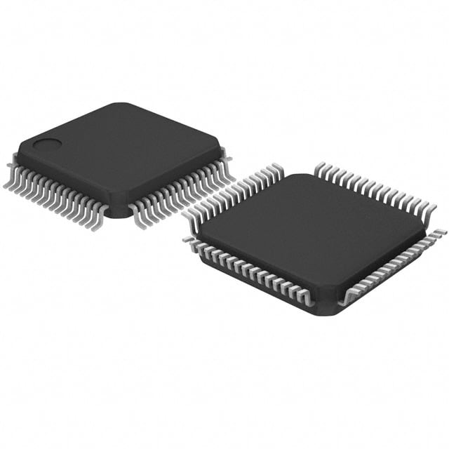
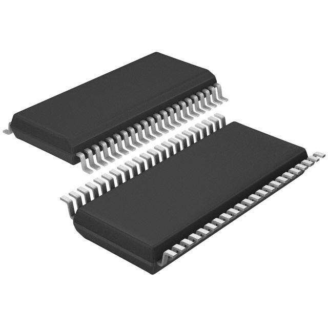
| 描述 | IC TUNER AM/FM CAR RADIO 64LQFP |
| 产品分类 | |
| 品牌 | STMicroelectronics |
| 数据手册 | |
| 产品图片 |
|
| 产品型号 | TDA7705 |
| rohs | 无铅 / 符合限制有害物质指令(RoHS)规范要求 |
| 产品系列 | - |
| 供应商器件封装 | 64-LQFP(10x10) |
| 其它名称 | 497-11728 |
| 其它有关文件 | http://www.st.com/web/catalog/sense_power/FM1934/CL1935/SC201/PF161593?referrer=70071840 |
| 包装 | 托盘 |
| 天线连接器 | PCB,表面贴装 |
| 存储容量 | - |
| 封装/外壳 | 64-LQFP |
| 工作温度 | -40°C ~ 85°C |
| 应用 | 车载音频 |
| 数据接口 | PCB,表面贴装 |
| 数据速率(最大值) | - |
| 标准包装 | 160 |
| 灵敏度 | - |
| 特性 | - |
| 电压-电源 | 4.75 V ~ 5.25 V |
| 电流-接收 | 220mA |
| 调制或协议 | AM,FM |
| 频率 | - |


- 商务部:美国ITC正式对集成电路等产品启动337调查
- 曝三星4nm工艺存在良率问题 高通将骁龙8 Gen1或转产台积电
- 太阳诱电将投资9.5亿元在常州建新厂生产MLCC 预计2023年完工
- 英特尔发布欧洲新工厂建设计划 深化IDM 2.0 战略
- 台积电先进制程称霸业界 有大客户加持明年业绩稳了
- 达到5530亿美元!SIA预计今年全球半导体销售额将创下新高
- 英特尔拟将自动驾驶子公司Mobileye上市 估值或超500亿美元
- 三星加码芯片和SET,合并消费电子和移动部门,撤换高东真等 CEO
- 三星电子宣布重大人事变动 还合并消费电子和移动部门
- 海关总署:前11个月进口集成电路产品价值2.52万亿元 增长14.8%


PDF Datasheet 数据手册内容提取
TDA7705 Highly integrated tuner for AM/FM car radio Features ■ Fully integrated VCO for world tuning ■ High performance PLL for fast RDS system ■ AM/FM mixers with high image rejection ■ Integrated AM-LNA and AM-PINDIODE ■ Automatic self alignment for preselection and image rejection ■ Digital IF signal processing, high performance LQFP64 and drift-free ■ Integrated IF-filters with high selectivity, high dynamic range and adaptive bandwidth control ■ RDS demodulation with group and block synchronization It contains mixers and IF amplifiers for AM and ■ High performance stereodecoder with FM, fully integrated VCO and PLL synthesizer, noiseblanker IF-processing including adaptive bandwidth ■ I2C/SPI bus controlled control, stereo decoder and RDS decoder on a single chip. ■ Single 5 V supply ■ LQFP64 package The utilization of digital signal processing results in numerous advantages against today's tuners: Description very low number of external components, very small space occupation and easy application, The TDA7705 highly integrated tuner (HIT) is a very high selectivity due to digital filters, high new generation of high performance tuners for flexibility by software control and automatic carradio applications. alignment. T able 1. Device summary Order code Package Packing TDA7705 LQFP64 (10x10x1.4mm) Tray TDA7705TR LQFP64 (10x10x1.4mm) Tape and reel September 2013 Doc ID 15938 Rev 9 1/42 www.st.com 1
Contents TDA7705 Contents 1 Block diagram and pins description . . . . . . . . . . . . . . . . . . . . . . . . . . . . 6 1.1 Block diagram . . . . . . . . . . . . . . . . . . . . . . . . . . . . . . . . . . . . . . . . . . . . . . . 6 1.2 Pin description . . . . . . . . . . . . . . . . . . . . . . . . . . . . . . . . . . . . . . . . . . . . . . 7 2 Function description . . . . . . . . . . . . . . . . . . . . . . . . . . . . . . . . . . . . . . . . 10 2.1 FM - mixers . . . . . . . . . . . . . . . . . . . . . . . . . . . . . . . . . . . . . . . . . . . . . . . 10 2.2 FM - AGC . . . . . . . . . . . . . . . . . . . . . . . . . . . . . . . . . . . . . . . . . . . . . . . . . 10 2.3 AM - LNA . . . . . . . . . . . . . . . . . . . . . . . . . . . . . . . . . . . . . . . . . . . . . . . . . 10 2.4 AM - AGC . . . . . . . . . . . . . . . . . . . . . . . . . . . . . . . . . . . . . . . . . . . . . . . . . 10 2.5 AM - mixers . . . . . . . . . . . . . . . . . . . . . . . . . . . . . . . . . . . . . . . . . . . . . . . 10 2.6 IF A/D converters . . . . . . . . . . . . . . . . . . . . . . . . . . . . . . . . . . . . . . . . . . . 11 2.7 Audio D/A converters . . . . . . . . . . . . . . . . . . . . . . . . . . . . . . . . . . . . . . . . 11 2.8 VCO . . . . . . . . . . . . . . . . . . . . . . . . . . . . . . . . . . . . . . . . . . . . . . . . . . . . . 11 2.9 PLL . . . . . . . . . . . . . . . . . . . . . . . . . . . . . . . . . . . . . . . . . . . . . . . . . . . . . . 11 2.10 Crystal oscillator . . . . . . . . . . . . . . . . . . . . . . . . . . . . . . . . . . . . . . . . . . . . 11 2.11 DSP . . . . . . . . . . . . . . . . . . . . . . . . . . . . . . . . . . . . . . . . . . . . . . . . . . . . . 11 2.12 IO interface pins . . . . . . . . . . . . . . . . . . . . . . . . . . . . . . . . . . . . . . . . . . . . 12 2.13 Serial interface . . . . . . . . . . . . . . . . . . . . . . . . . . . . . . . . . . . . . . . . . . . . . 12 2.13.1 Serial interface choice / boot mode . . . . . . . . . . . . . . . . . . . . . . . . . . . . 12 2.13.2 I2C bus protocol . . . . . . . . . . . . . . . . . . . . . . . . . . . . . . . . . . . . . . . . . . . 13 2.13.3 SPI bus protocol . . . . . . . . . . . . . . . . . . . . . . . . . . . . . . . . . . . . . . . . . . 14 3 Electrical specifications . . . . . . . . . . . . . . . . . . . . . . . . . . . . . . . . . . . . . 16 3.1 Absolute maximum ratings . . . . . . . . . . . . . . . . . . . . . . . . . . . . . . . . . . . . 16 3.2 Thermal data . . . . . . . . . . . . . . . . . . . . . . . . . . . . . . . . . . . . . . . . . . . . . . 16 3.3 General key parameters . . . . . . . . . . . . . . . . . . . . . . . . . . . . . . . . . . . . . . 16 3.4 Electrical characteristics . . . . . . . . . . . . . . . . . . . . . . . . . . . . . . . . . . . . . . 17 3.4.1 FM - section . . . . . . . . . . . . . . . . . . . . . . . . . . . . . . . . . . . . . . . . . . . . . . 17 3.4.2 AM - section . . . . . . . . . . . . . . . . . . . . . . . . . . . . . . . . . . . . . . . . . . . . . . 18 3.4.3 VCO . . . . . . . . . . . . . . . . . . . . . . . . . . . . . . . . . . . . . . . . . . . . . . . . . . . . 19 3.4.4 Phase locked loop . . . . . . . . . . . . . . . . . . . . . . . . . . . . . . . . . . . . . . . . . 19 3.4.5 Tuning DAC . . . . . . . . . . . . . . . . . . . . . . . . . . . . . . . . . . . . . . . . . . . . . . 19 2/42 Doc ID 15938 Rev 9
TDA7705 Contents 3.4.6 IF ADC . . . . . . . . . . . . . . . . . . . . . . . . . . . . . . . . . . . . . . . . . . . . . . . . . . 19 3.4.7 Audio DAC . . . . . . . . . . . . . . . . . . . . . . . . . . . . . . . . . . . . . . . . . . . . . . . 20 3.4.8 IO interface pins . . . . . . . . . . . . . . . . . . . . . . . . . . . . . . . . . . . . . . . . . . . 20 3.4.9 I2C interface . . . . . . . . . . . . . . . . . . . . . . . . . . . . . . . . . . . . . . . . . . . . . . 21 3.4.10 SPI interface . . . . . . . . . . . . . . . . . . . . . . . . . . . . . . . . . . . . . . . . . . . . . 22 3.4.11 Warning . . . . . . . . . . . . . . . . . . . . . . . . . . . . . . . . . . . . . . . . . . . . . . . . . 22 3.5 Overall system performance . . . . . . . . . . . . . . . . . . . . . . . . . . . . . . . . . . 23 3.5.1 FM overall system performance . . . . . . . . . . . . . . . . . . . . . . . . . . . . . . . 23 3.5.2 AM MW overall system performance . . . . . . . . . . . . . . . . . . . . . . . . . . . 25 3.5.3 AM LW overall system performance . . . . . . . . . . . . . . . . . . . . . . . . . . . 27 3.5.4 AM SW overall system performance . . . . . . . . . . . . . . . . . . . . . . . . . . . 28 3.5.5 WX overall system performance . . . . . . . . . . . . . . . . . . . . . . . . . . . . . . 29 4 Front-end processing . . . . . . . . . . . . . . . . . . . . . . . . . . . . . . . . . . . . . . . 30 5 Weak signal processing . . . . . . . . . . . . . . . . . . . . . . . . . . . . . . . . . . . . . 33 5.1 FM IF-processing . . . . . . . . . . . . . . . . . . . . . . . . . . . . . . . . . . . . . . . . . . . 33 5.1.1 Dynamic channel selection filter (DISS) . . . . . . . . . . . . . . . . . . . . . . . . 33 5.1.2 Soft mute . . . . . . . . . . . . . . . . . . . . . . . . . . . . . . . . . . . . . . . . . . . . . . . . 33 5.1.3 Adjacent channel mute . . . . . . . . . . . . . . . . . . . . . . . . . . . . . . . . . . . . . 34 5.1.4 Stereo blend- . . . . . . . . . . . . . . . . . . . . . . . . . . . . . . . . . . . . . . . . . . . . . 34 5.1.5 High cut control . . . . . . . . . . . . . . . . . . . . . . . . . . . . . . . . . . . . . . . . . . . 35 5.1.6 Stereo decoder . . . . . . . . . . . . . . . . . . . . . . . . . . . . . . . . . . . . . . . . . . . 36 5.2 AM IF-processing . . . . . . . . . . . . . . . . . . . . . . . . . . . . . . . . . . . . . . . . . . . 36 5.2.1 Channel selection filter . . . . . . . . . . . . . . . . . . . . . . . . . . . . . . . . . . . . . 36 5.2.2 Soft mute . . . . . . . . . . . . . . . . . . . . . . . . . . . . . . . . . . . . . . . . . . . . . . . . 36 5.2.3 High cut control . . . . . . . . . . . . . . . . . . . . . . . . . . . . . . . . . . . . . . . . . . . 37 6 Application schematics . . . . . . . . . . . . . . . . . . . . . . . . . . . . . . . . . . . . . 38 6.1 Basic application schematic . . . . . . . . . . . . . . . . . . . . . . . . . . . . . . . . . . . 38 6.2 Application schematic example with SPI-bus and tuned preselection . . . 39 7 Package information . . . . . . . . . . . . . . . . . . . . . . . . . . . . . . . . . . . . . . . . 40 8 Revision history . . . . . . . . . . . . . . . . . . . . . . . . . . . . . . . . . . . . . . . . . . . 41 Doc ID 15938 Rev 9 3/42
List of tables TDA7705 List of tables Table 1. Device summary. . . . . . . . . . . . . . . . . . . . . . . . . . . . . . . . . . . . . . . . . . . . . . . . . . . . . . . . . . 1 Table 2. Pin description . . . . . . . . . . . . . . . . . . . . . . . . . . . . . . . . . . . . . . . . . . . . . . . . . . . . . . . . . . . 7 Table 3. Boot mode pin configuration. . . . . . . . . . . . . . . . . . . . . . . . . . . . . . . . . . . . . . . . . . . . . . . . 13 Table 4. Absolute maximum ratings. . . . . . . . . . . . . . . . . . . . . . . . . . . . . . . . . . . . . . . . . . . . . . . . . 16 Table 5. Thermal data. . . . . . . . . . . . . . . . . . . . . . . . . . . . . . . . . . . . . . . . . . . . . . . . . . . . . . . . . . . . 16 Table 6. General key parameters. . . . . . . . . . . . . . . . . . . . . . . . . . . . . . . . . . . . . . . . . . . . . . . . . . . 16 Table 7. FM - section . . . . . . . . . . . . . . . . . . . . . . . . . . . . . . . . . . . . . . . . . . . . . . . . . . . . . . . . . . . . 17 Table 8. AM - section . . . . . . . . . . . . . . . . . . . . . . . . . . . . . . . . . . . . . . . . . . . . . . . . . . . . . . . . . . . . 18 Table 9. VCO . . . . . . . . . . . . . . . . . . . . . . . . . . . . . . . . . . . . . . . . . . . . . . . . . . . . . . . . . . . . . . . . . . 19 Table 10. Phase locked loop . . . . . . . . . . . . . . . . . . . . . . . . . . . . . . . . . . . . . . . . . . . . . . . . . . . . . . . 19 Table 11. Tuning DAC . . . . . . . . . . . . . . . . . . . . . . . . . . . . . . . . . . . . . . . . . . . . . . . . . . . . . . . . . . . . 19 Table 12. IF ADC . . . . . . . . . . . . . . . . . . . . . . . . . . . . . . . . . . . . . . . . . . . . . . . . . . . . . . . . . . . . . . . . 19 Table 13. Audio DAC . . . . . . . . . . . . . . . . . . . . . . . . . . . . . . . . . . . . . . . . . . . . . . . . . . . . . . . . . . . . . 20 Table 14. IO interface pins . . . . . . . . . . . . . . . . . . . . . . . . . . . . . . . . . . . . . . . . . . . . . . . . . . . . . . . . . 20 Table 15. I2C interface . . . . . . . . . . . . . . . . . . . . . . . . . . . . . . . . . . . . . . . . . . . . . . . . . . . . . . . . . . . . 21 Table 16. SPI interface. . . . . . . . . . . . . . . . . . . . . . . . . . . . . . . . . . . . . . . . . . . . . . . . . . . . . . . . . . . . 22 Table 17. FM overall system performance. . . . . . . . . . . . . . . . . . . . . . . . . . . . . . . . . . . . . . . . . . . . . 23 Table 18. AM MW overall system performance . . . . . . . . . . . . . . . . . . . . . . . . . . . . . . . . . . . . . . . . . 25 Table 19. AM LW overall system performance. . . . . . . . . . . . . . . . . . . . . . . . . . . . . . . . . . . . . . . . . . 27 Table 20. AM SW overall system performance . . . . . . . . . . . . . . . . . . . . . . . . . . . . . . . . . . . . . . . . . 28 Table 21. WX overall system performance. . . . . . . . . . . . . . . . . . . . . . . . . . . . . . . . . . . . . . . . . . . . . 29 Table 22. Register 0x00 . . . . . . . . . . . . . . . . . . . . . . . . . . . . . . . . . . . . . . . . . . . . . . . . . . . . . . . . . . . 30 Table 23. Register 0x01 . . . . . . . . . . . . . . . . . . . . . . . . . . . . . . . . . . . . . . . . . . . . . . . . . . . . . . . . . . . 31 Table 24. Register 0x02 . . . . . . . . . . . . . . . . . . . . . . . . . . . . . . . . . . . . . . . . . . . . . . . . . . . . . . . . . . . 31 Table 25. Register 0x05 . . . . . . . . . . . . . . . . . . . . . . . . . . . . . . . . . . . . . . . . . . . . . . . . . . . . . . . . . . . 32 Table 26. Dynamic channel selection filter (DISS). . . . . . . . . . . . . . . . . . . . . . . . . . . . . . . . . . . . . . . 33 Table 27. Soft mute . . . . . . . . . . . . . . . . . . . . . . . . . . . . . . . . . . . . . . . . . . . . . . . . . . . . . . . . . . . . . . 33 Table 28. Adjacent channel mute. . . . . . . . . . . . . . . . . . . . . . . . . . . . . . . . . . . . . . . . . . . . . . . . . . . . 34 Table 29. Stereo blend. . . . . . . . . . . . . . . . . . . . . . . . . . . . . . . . . . . . . . . . . . . . . . . . . . . . . . . . . . . . 34 Table 30. High cut control. . . . . . . . . . . . . . . . . . . . . . . . . . . . . . . . . . . . . . . . . . . . . . . . . . . . . . . . . . 35 Table 31. De-emphasis filter. . . . . . . . . . . . . . . . . . . . . . . . . . . . . . . . . . . . . . . . . . . . . . . . . . . . . . . . 36 Table 32. Stereo decoder. . . . . . . . . . . . . . . . . . . . . . . . . . . . . . . . . . . . . . . . . . . . . . . . . . . . . . . . . . 36 Table 33. Channel selection filter. . . . . . . . . . . . . . . . . . . . . . . . . . . . . . . . . . . . . . . . . . . . . . . . . . . . 36 Table 34. Soft mute . . . . . . . . . . . . . . . . . . . . . . . . . . . . . . . . . . . . . . . . . . . . . . . . . . . . . . . . . . . . . . 36 Table 35. High cut control. . . . . . . . . . . . . . . . . . . . . . . . . . . . . . . . . . . . . . . . . . . . . . . . . . . . . . . . . . 37 Table 36. Document revision history . . . . . . . . . . . . . . . . . . . . . . . . . . . . . . . . . . . . . . . . . . . . . . . . . 41 4/42 Doc ID 15938 Rev 9
TDA7705 List of figures List of figures Figure 1. Functional block diagram . . . . . . . . . . . . . . . . . . . . . . . . . . . . . . . . . . . . . . . . . . . . . . . . . . . 6 Figure 2. Pin connection (top view) . . . . . . . . . . . . . . . . . . . . . . . . . . . . . . . . . . . . . . . . . . . . . . . . . . . 7 Figure 3. I2C "write" sequence. . . . . . . . . . . . . . . . . . . . . . . . . . . . . . . . . . . . . . . . . . . . . . . . . . . . . . 13 Figure 4. I2C "read" sequence. . . . . . . . . . . . . . . . . . . . . . . . . . . . . . . . . . . . . . . . . . . . . . . . . . . . . . 14 Figure 5. SPI modes . . . . . . . . . . . . . . . . . . . . . . . . . . . . . . . . . . . . . . . . . . . . . . . . . . . . . . . . . . . . . 15 Figure 6. SPI "write" sequence . . . . . . . . . . . . . . . . . . . . . . . . . . . . . . . . . . . . . . . . . . . . . . . . . . . . . 15 Figure 7. SPI "read" sequence. . . . . . . . . . . . . . . . . . . . . . . . . . . . . . . . . . . . . . . . . . . . . . . . . . . . . . 15 Figure 8. I2C bus timing diagram. . . . . . . . . . . . . . . . . . . . . . . . . . . . . . . . . . . . . . . . . . . . . . . . . . . . 21 Figure 9. SPI bus timing diagram. . . . . . . . . . . . . . . . . . . . . . . . . . . . . . . . . . . . . . . . . . . . . . . . . . . . 22 Figure 10. FM input set-up. . . . . . . . . . . . . . . . . . . . . . . . . . . . . . . . . . . . . . . . . . . . . . . . . . . . . . . . . . 23 Figure 11. AM MW input set up. . . . . . . . . . . . . . . . . . . . . . . . . . . . . . . . . . . . . . . . . . . . . . . . . . . . . . 25 Figure 12. AM LW input set-up . . . . . . . . . . . . . . . . . . . . . . . . . . . . . . . . . . . . . . . . . . . . . . . . . . . . . . 27 Figure 13. AM SW input set-up . . . . . . . . . . . . . . . . . . . . . . . . . . . . . . . . . . . . . . . . . . . . . . . . . . . . . . 28 Figure 14. WX input set-up . . . . . . . . . . . . . . . . . . . . . . . . . . . . . . . . . . . . . . . . . . . . . . . . . . . . . . . . . 29 Figure 15. FM wide-band application / I2C control. . . . . . . . . . . . . . . . . . . . . . . . . . . . . . . . . . . . . . . . 38 Figure 16. Example of FM tuned (narrow-band) application / SPI control. . . . . . . . . . . . . . . . . . . . . . 39 Figure 17. LQFP64 (10x10x1.4mm) mechanical data and package dimensions. . . . . . . . . . . . . . . . . 40 Doc ID 15938 Rev 9 5/42
Block diagram and pins description TDA7705 1 Block diagram and pins description 1.1 Block diagram Figure 1. Functional block diagram TT NN SISI DD RR SS PP DD SS RR DD SSUUMM OO LL NCNC DLDL C/C/ PIPI 22II SS utut ADCADC ADCADC STEREO STEREO DACDAC Audio OAudio O CC SS OO FF yy : 8: 8 FREFRE uppluppl SS LL LL PP CC GG OO AA NN CC : : VV CC AA DD CC GG AA MM AA 6/42 Doc ID 15938 Rev 9
TDA7705 Block diagram and pins description 1.2 Pin description Figure 2. Pin connection (top view) C C GND-VCO VCC-VCO LFref VCOdec GND-PLL VCC-PLL VCC-IFAD LIFrefH LIFrefL GND-IFAD DACoutR DACoutL GND-DAC OSCin OSCout VCC-DAC 64 63 62 61 60 59 58 57 56 55 54 53 52 51 50 49 LFI 1 48 GND-1V2 PLLTEST 2 47 VDD-1V2 DAC 3 46 TEST TCAGCFM 4 45 RSTN FMMIX1dec 5 44 MODE FMMIX1in 6 43 GPIO0 FMMIX2in 7 42 GPIO1 GND-RF 8 41 GPIO2 FMPINDRV 9 40 GPIO3 VCC-RF 10 39 RDSINT TCAM 11 38 VDD-1V2 AMPINDRV 12 37 SCL/CLK PINDdec 13 36 SDA/MOSI PINDin 14 35 SPI_MISO GND-LNA 15 34 SPI_CS LNAin 16 33 GND-3V3 17 18 19 20 21 22 23 24 25 26 27 28 29 30 31 32 LNAdec LNAout LNAin2 LNAout2 LNAdec2 AMMIXin2 AMMIXin1 AMMIXdec GND-IF VREF165 VREFdec GND-DIG VCC-DIG VCCREG12 REG-1V2 VDD-3V3 AC00418 T able 2. Pin description Pin # Pin name Function 1 LF1 PLL loopfilter output 2 PLLTEST PLL test output / GPO 3 DAC FM tuning DAC output 4 TCAGCFM FM AGC time constant 5 FMMIX1dec FM mixer decoupling 6 FMIX1in FM mixer input 1 7 FMIX2in FM mixer input 2 8 GND-RF RF Ground 9 FMPINDRV FM AGC PIN diode driver 10 VCC-RF 5V supply for RF section 11 TCAM AM AGC time constant 12 AMPINDRV AM AGC external PIN diode driver 13 PINDdec AM AGC internal PIN diode decoupling 14 PINDin AM AGC internal PIN diode input 15 GND-LNA AM LNA and internal PIN diode GND 16 LNAin AM LNA input Doc ID 15938 Rev 9 7/42
Block diagram and pins description TDA7705 Table 2. Pin description (continued) Pin # Pin name Function 17 LNAdec AM LNA decoupling 18 LNAout AM LNA output first stage 19 LNAin2 AM LNA input 2nd stage 20 LNAout2 AM LNA output 21 LNAdec2 AM LNA decoupling 2nd stage 22 AMMIXin2 AM mixer input 2 23 AMMIXin1 AM mixer input 1 24 AMMIXdec AM mixer decoupling 25 GND-IF IF and Vref GND 26 VREF165 1.65V reference voltage decoupling 27 VREFdec 3.3V reference voltage decoupling 28 GND-DIG Digital GND 29 VCC-DIG 5V supply for digital logic 30 VCCreg1V2 VCC of 1.2V regulator 31 REG1V2 1.2V regulator output 32 VDD-3V3 3.3V VDD output / decoupling 33 GND-3V3 3.3V VDD GND 34 SPI_CS SPI chip select 35 SPI_MISO SPI Data output 36 SDA / SPI_MOSI I2C bus data / SPI data input 37 SCL / SPI_CLK I2C bus Clock / SPI clock 38 VDD-1V2 1.2V DSP supply 39 RDSINT RDS interrupt 40 GPIO3 Reserved 41 GPIO2 Reserved 42 GPIO 1 Reserved 43 GPIO 0 Reserved 44 MODE For debug purpose only, connected to GND 45 RSTN Reset pin (active low) 46 TEST Test input 47 VDD-1V2 1.2V DSP supply 48 GND-1V2 Digital GND for 1.2V VDD 49 VCC-DAC 5V supply of audio DAC 50 OSCout Xtal osc output 51 OSCin Xtal osc input 8/42 Doc ID 15938 Rev 9
TDA7705 Block diagram and pins description Table 2. Pin description (continued) Pin # Pin name Function 52 GND-DAC Audio DAC GND 53 DACoutL Audio output left 54 DACoutR Audio output right 55 GND-IFADC IF ADC GND 56 LIFrefL IF ADC reference low 57 LIFrefH IF ADC reference high 58 VCC-IFADC 5V supply of IF ADC 59 VCC-PLL 5V supply of PLL 60 GND-PLL PLL GND 61 VCO-dec VCO decoupling 62 LFref Loopfilter reference 63 VCC-VCO 5V supply of VCO 64 GND-VCO VCO GND Doc ID 15938 Rev 9 9/42
Function description TDA7705 2 Function description 2.1 FM - mixers The image-rejection mixer has two FM inputs, selectable through software. These inputs feed stages with different gains, noise figures, and IIP3. They are optimized for best performance in case of a passive tuned prestage and for a passive fixed bandpass without tuning for low-cost application respectively. The second input offers also the possibility of an easy addition of a weather-band preselection filter. The input frequency is downconverted to low IF with high image rejection. The tuned application is supported by an 8-bit tuning DAC. The alignment of the DAC is performed automatically. 2.2 FM - AGC The programmable RFAGC senses the mixer input whereas the IFAGC senses the IFADC input to avoid overload. The PIN diode driver is able to drive external PIN diodes with a current value as high as 15mA. The time constant of the FM-AGC is defined by an external capacitor. 2.3 AM - LNA The AM-LNA is integrated with low noise and high IIP2 and IIP3. The gain of the LNA is controlled by the AGC. The maximum gain is set with an external resistor, typically 26 dB with 1 k. 2.4 AM - AGC The programmable AM-RF-AGC senses the mixer inputs and controls the internal PIN diode and LNA gain. First the LNA gain is reduced by about 10dB, then the PIN diodes are activated to attenuate the signal. The time constant of the AM-AGC is defined with an external capacitor and programmable internal currents. 2.5 AM - mixers The image-rejection mixer has two AM inputs selectable via software. It easily supports low- cost applications for extended frequency bands like SW, DRM. The input frequency is converted to low IF with high image rejection. 10/42 Doc ID 15938 Rev 9
TDA7705 Function description 2.6 IF A/D converters A high performance IQ-IFADC converts the IF-signal to digital IF for subsequent digital signal processing. 2.7 Audio D/A converters A stereo DAC provides the left / right audio signals after IF-processing and stereodecoding by the DSP. 2.8 VCO The VCO is fully integrated without any external tuning component. It covers all FM frequency bands including EU, US , Japan, EastEU, Weatherband and AM-bands including LW, MW, SW. 2.9 PLL The high speed tuning PLL is able to settle within about 300 µs for fast RDS applications. The frequency step can be as low as 5 kHz in FM and 500 Hz in AM. 2.10 Crystal oscillator The device works with a 37.05 MHz fundamental tone crystal, and can be used also with a 3rd overtone 37.05 MHz crystal. 2.11 DSP The DSP and its hardware accelerators perform all the digital signal processing. The main program is fixed in ROM. Control parameters are copied in RAM and are accessible and modifiable there, thus allowing parametric performance optimization. It performs: ● digital down-conversion of IF ● bandwidth selection with variable controlled bandwidth ● FM and AM noiseblanking ● FM/AM demodulation with softmute, high-cut, weak signal processing and quality detection ● FM stereo decoding with stereo blend ● RDS demodulation including error correction and block synchronization with generation of an RDS interrupt for the main µP ● Autonomous control of RDS-AF tests ● Self alignment of preselection tuning Doc ID 15938 Rev 9 11/42
Function description TDA7705 2.12 IO interface pins The TDA7705 has the following IO pins: PLLTEST pin 2 general purpose output SPI_CS pin 34 serial communication with µP SPI_MISO pin 35 serial communication with µP SDA/MOSI pin 36 serial communication with µP SCL/CLK pin 37 serial communication with µP RDSINT pin 39 serial communication with µP RSTN pin 45 reset pin driven by µP The pins labeled GPIO0, 1, 2 and 3 (pins 43 to 40) are reserved. The pin PLLTEST output voltage can be freely programmed via software and be used to drive switches if needed by the application. All the inputs are voltage-tolerant up to 3.5 V . The outputs can drive currents up to 0.5 mA from the internal 3.3 V supply line. 2.13 Serial interface The device is controlled with a standard I2C bus or SPI interface. Through the serial bus the processing parameters can be modifed and the signal quality parameters and the RDS information can be read out. The operation of the device is handled through high level commands sent by the main car- radio µP through the serial interface, which allow to simplify the operations carried out in the main µP. The high level commands include among others: ● set frequency (which allows to avoid computing the PLL divider factors); ● start seek (the seek operation can be carried out by the TDA7705 in a completely autonomous fashion); ● RDS seek/search (jumps to AF and quality measurements are automatically sequenced). 2.13.1 Serial interface choice / boot mode The device can communicate with the main µP with two different standard serial protocols: SPI and I2C. The configuration is chosen by setting the proper value (0V or 3.3V) at pins 35 and 39 and it is latched (e.g. made effective) when the RSTN line transitions from low to high (when RSTN is low, the IC is in reset mode). The voltage level forced to pins 35 and 39 must be released to start the system operation a suitable time after the RSTN line has gone high. The list of configurations is shown in the following table: 12/42 Doc ID 15938 Rev 9
TDA7705 Function description T able 3. Boot mode pin configuration Configuration: I2C (addr. 0 x C2) I2C (addr. 0 x C8) SPI Pin at reset operation at reset operation at reset operation 0 RDS interrupt 0 RDS interrupt 1 RDS interrupt 39 RDSINT in out in out in out I2C SCL I2C SCL SPI CLK 37 SCL x x x in in in I2C SDA I2C SDA SPI MOSI 36 SDA x x x in/out in/out in 0 1 1 SPI MISO 35 (SPI_MISO) - - in in in out SPI SS 34 (SPI_CS) x - x - x in If I2C serial bus is chosen as means of communication with the controlling device, two chip addresses are possible: 0xC2/C3 or 0xC8/C9, depending on the initial configuration of pins 35 and 39. The status of pins 35 and 39 during the reset phase can be set to: high, through external <10 k resistors tied to 3.3V (pin 32), or low, by not forcing any voltage on them from outside, as 50 kohm internal pull-down resistors are present on said pins. To make sure the boot mode is correctly latched up at start-up, it is advisable to keep the RSTN line low until the IC supply pins have reached their steady state, and then for an additional time T (see Section3.4.8). reset 2.13.2 I2C bus protocol I2C requires two signals: clock (SCL) and data (SDA - bidirectional). The protocol requires an acknowledge after any 8-bit transmission. A "write" communication example is shown in the figure below, for an unspecified number of data bytes (see the relevant technical documentation for frame structure description): Figure 3. I2C "write" sequence SDA a7 a6 … a0 d7 d6 … d0 SCL clk1 clk2 … clk8 clk9 clk1 clk2 … clk8 clk9 START address ACK data ACK STOP Doc ID 15938 Rev 9 13/42
Function description TDA7705 The sequence consists of the following phases: ● START: SDA line transitioning from H to L with SCL fixed H. This signifies a new transmission is starting; ● data latching: on the rising SCL edge. The SDA line can transition only when SCL is low (otherwise its transitions are interpreted as either a START or a STOP transition); ● ACKnowledge: on the 9th SCL pulse the µP keeps the SDA line H, and the TDA7705 pulls it down if communication has been successful. Lack of the acknowledge pulse generation from the TDA7705 means that the communication has failed; ● a chip address byte must be sent at the beginning of the transmission. The value can be C2 or C8 (according to the mode chosen at start-up during boot) for "write"; ● as many data bytes as needed can follow the address before the communication is terminated. See the next section for details on the frame format; ● STOP: SDA line transitioning from L to H with SCL H. This signifies the end of the transmission. Red lines represent transmissions from the TDA7705 to the µP. A "read" communication example is shown in the figure below, for an unspecified number of data bytes (see later on for frame structure decription): Figure 4. I2C "read" sequence SDA a7 a6 … a0 d7 d6 … d0 SCL clk1 clk2 … clk8 clk9 clk1 clk2 … clk8 clk9 START address ACK data ACK STOP The sequence is very similar to the "write" one and has the same constraints for start, stop, data latching. The differences follow: ● a chip address must always be sent by the µP to the TDA7705; the address must be C3 (if C2 had been selected at boot) or C9 (if C8 had been selected at boot); ● a header is transmitted after the chip address (the same happens for "write") before data are transferred from the TDA7705 to the µP. See the relevant technical documentation for details on the frame format; ● when data are transmitted from the TDA7705 to the µP, the µP keeps the SDA line H; ● the ACKnowledge pulse is generated by the µP for those data bytes that are sent by the TDA7705 to the µP. Failure of the µP to generate an ACK pulse on the 9th CLK pulse has the same effect on the TDA7705 as a STOP. The max. clock speed is 500 kbit/s. 2.13.3 SPI bus protocol SPI requires four signals: clock (CLK), master output/slave input (MOSI - for communication from the µP to the TDA7705), master input/slave output (MISO - for communication from the TDA7705 to the µP), chip select (CS). CLK is generated by the master device and is used for synchronization. MOSI and MISO are the data lines. The CS line is unique for each device in an SPI bus. The µP pulls low the TDA7705 CS line to select it for communication. The protocol does not foresee any transmission acknowledgement. The SPI protocol has four possible modes of operation as far as data latching is concerned: 14/42 Doc ID 15938 Rev 9
TDA7705 Function description Figure 5. SPI modes In the case of the TDA7705, the data are latched on the clock's rising edge, with CPOL = 1 and CPHA = 1 (mode 3 in the figure above). According to the specification of this mode, the polarity of the CLK line when no communication is taking place is high. A "write" communication example is shown in the figure below, for an unspecified number of bits (see the relevant technical documentation for frame structure description): Figure 6. SPI "write" sequence CS CLK MOSI MSB ... ... ... ... ... ... ... ... ... ... LSB The start condition is signaled by the CS line going low, and the stop condition by the CS line going high. It is not allowed to toggle the CS line while the communication is going on. A "read" communication example is shown in the figure below, for an unspecified number of bits (see the relevant technical documentation for frame structure description ): Figure 7. SPI "read" sequence CS CLK MOSI MSB ... ... ... ... LSB MISO MSB ... ... ... ... LSB The red line is controlled by the TDA7705, whereas the black lines are controlled by the µP. Doc ID 15938 Rev 9 15/42
Electrical specifications TDA7705 3 Electrical specifications 3.1 Absolute maximum ratings Table 4. A bsolute maximum ratings Symbol Parameter Test condition Min Typ Max Units V Supply voltage - - - 5.5 V CC T Storage temperature - -55 - 150 °C stg Human body model ±2000 Charged device model ±450 V ESD withstand voltage V ESD Charged device model, corner pins ±750 Machine model ±150 3.2 Thermal data T able 5. Thermal data Symbol Parameter Test condition Value Units Thermal resistance R LQFP64 10x10, double-layer JEDEC PCB 55 °C/W Th j-amb junction-to-ambient 3.3 General key parameters Table 6. G eneral key parameters Symbol Parameter Test condition Min Typ Max Units V 5 V supply voltage - 4.7 5 5.25 V CC I Supply current @ 5 V - - 220 295 mA CC T Ambient temperature range - -40 - 85 °C amb V VCCREG12 supply voltage see note(1) 2 - - V VCCREG12 Digital core 1.2V supply when supplied externally V 1.08 1.2 1.32 V 1V2 voltage see note (2) V = 1.08 V 1V2 - - 120 mA see note (2) Digital core 1.2 V supply V = 1.2 V I 1V2 - 80 135 mA 1V2 current see note (2) V = 1.32 V 1V2 - - 150 mA see note (2) 1. In the typical application supplied from 5V with a series resistor. 2. When the 1.2 V supply is applied externally, and not using the internal 1.2 V regulator. 16/42 Doc ID 15938 Rev 9
TDA7705 Electrical specifications 3.4 Electrical characteristics V = 4.7 V to 5.25 V; T = -40 °C to +85 °C; unless otherwise specified. CC amb 3.4.1 FM - section Table 7. F M - section Symbol Parameter Test condition Min Typ Max Units FM IMR mixer R Input resistance - 90 130 170 k in Mix 1, R = 1.5 k, source - 2.5 3.1 noiseless V Input noise voltage nV/Hz noise Mix 2, R = 800 , source - 2 2.5 noiseless Mix 1 122 125 dBµV up to V = 90 dBµV IIP3 3rd order intercept point in/tone - Mix 2 118 121 dBµV up to V = 85 dBµV in/tone FM AGC Mix 1, min setting - 87 - RFAGC threshold, referred to Mix 1, max setting - 93 - mixer input; dBµV Mix 2, min setting - 85 - RF level RFAGC-Thr Mix 2, max setting - 91 - Threshold steps - - 2 - dB Threshold error @ T = 27 °C -1.5 1.5 dB amb Threshold temperature drift - 0.016 - dB/K Mix 1, min setting - 81 - IFAGC threshold, referred to mixer input; at tuned Mix 1, max setting - 85 - dBµV frequency Mix 2, min setting - 77 - RF level IFAGC-Thr Mix 2, max setting - 81 - Threshold steps - - 2 - dB Threshold error @ T = 27 °C -1.5 1.5 dB amb Threshold temperature drift - 0.016 - dB/K - Pin diode source current @ T = 27 °C; see note(1) 12 - - mA amb - Pin diode sink current - 3 - 20 µA Pin diode source current in - @ T = 27 °C; see note(1) 0.4 - - mA constant current mode amb 1. The current is generated by a PTAT (Proportional To Absolute Temperature) source, and has therefore a temperature dependency described by: I/Io = T/To, with Io being the current at ambient temperature (25 °C) and To the ambient temperature (25°C) expressed in Kelvin, that is 298 K. Doc ID 15938 Rev 9 17/42
Electrical specifications TDA7705 3.4.2 AM - section Table 8. A M - section Symbol Parameter Test condition Min Typ Max Units AM IMR Mixer R Input resistance - 20 30 45 k in V Max. output voltage without clipping - 126 - dBµV out_max Mix 1, R = 1 k, source - 8.5 12 noiseless V Input noise voltage nV/Hz N,in Mix 2, R = 1 k, source - 8.5 12 noiseless Mix 1,2 IIP3 3rd order intercept point 126 129 - dBµV up to V = 90 dBµV in/tone Mix1 1,2 IIP2 2nd order intercept point - 158 - dBµV up to V = 90 dBµV in/tone N=2,3,4,5,6 - 100 - LO hsupp LO harmonic suppression dB N=7,9 - 85 - AM LNA Max Gain, R = 1 k 21 25 28 ext Gain Voltage gain dB Min Gain (AGC controlled) - 12 - R Input resistance - - 1000 k in C Input capacitance - - 20 pF in V Input noise voltage - - 1.0 1.4 nV/Hz N,in IIP3 3rd order intercept point @ maximum LNA gain - 125 - dBµV IIP2 2nd order intercept point @ maximum LNA gain - 143 - dBµV AM PIN diode Full attenuation, IIP2 2nd order intercept point - 140 - dBµV C = 80 pF, f=1 MHz source R Minimum resistance - - 50 80 min C Input capacitance High ohmic - 12 - pF in AM AGC Referred to mixer input Mix 1,2 min setting - 87 - AGC-Thr dBµV RF level Mix 1,2 max setting - 93 - Threshold steps - - 1 - Thr-steps Threshold error @ T = 27 °C -2.5 - 2.5 dB amb Threshold temperature drift - -3 - 3 - Pin diode source current @ T = 27 °C; see note(1) 2 - 10 mA amb - Pin diode sink current - 15 35 50 µA Pin diode source current in - @ T = 27 °C; see note(1) 1.5 2.5 3.5 mA constant current mode amb 1. The current is generated by a PTAT (Proportional To Absolute Temperature) source, and has therefore a temperature dependency described by: I/Io = T/To, with Io being the current at ambient temperature (25 °C) and To the ambient temperature (25 °C) expressed in Kelvin, that is 298 K. 18/42 Doc ID 15938 Rev 9
TDA7705 Electrical specifications 3.4.3 VCO Table 9. V CO Symbol Parameter Test condition Min Typ Max Units F Frequency range VCO - 1100 1550 MHz VCO Locked VCO; values referred @ 100MHz PN Phase noise of LO @ 100 Hz - -100 - dBc/Hz @ 1 kHz -115 @ 10 kHz -115 FM reception, deemphasis dev Deviation error (rms) - 5 - Hz 50µs, f = 20 Hz...20 kHz audio 3.4.4 Phase locked loop Table 10. P hase locked loop Symbol Parameter Test condition Min Typ Max Units T Settling time FM f < 10 kHz - 300 - µs settle FM step FM frequency step - - 5 - kHz AM step AM frequency step - - 500 - Hz 3.4.5 Tuning DAC Table 11. T uning DAC Symbol Parameter Test condition Min Typ Max Units Res Resolution 8 bit - 18 - mV V Min output voltage - - 0.6 0.7 V outmin V Max ouput voltage - VCC-0.2 VCC-0.1 - V outmax R Output impdedance - 1.5 2.5 3.5 k out DNL Diff. Non linearity - - - 0.5 LSB T Conversion time - - 20 - µs conv 3.4.6 IF ADC Table 12. I F ADC Symbol Parameter Test condition Min Typ Max Units DR Dynamic range in FM BW = ±200 kHz - 90 - dB FM mixer 1 1.1 1.9 V Input noise referred to mixer input - nV/Hz N,in FM mixer 2 0.7 1.2 DR Dynamic range in AM BW = ±4 kHz - 103 - dB AM V Input noise referred to mixer input - - 6.9 12 nV/Hz N,in AM Doc ID 15938 Rev 9 19/42
Electrical specifications TDA7705 3.4.7 Audio DAC Table 13. A udio DAC Symbol Parameter Test condition Min Typ Max Units V Max. output voltage Full scale - 1 - Vrms out BW Bandwidth 1dB attenuation - 15 - KHz R Output resistance - 600 750 900 out V Output noise - - 60 95 µVrms N, out THD Distortion -6 dBFS - 0.03 0.04 % 3.4.8 IO interface pins Table 14. I O interface pins Symbol Parameter Test condition Min Typ Max Units High level output voltage (all - I = 500 µA 2.9 3.2 - V IOs except GPO pin 2) out GPIOs source current (all IOs Total sourced current by all - - - 1.25 mA in source mode except pin 2) GPIOs Low level output voltage (all - I = -1 mA - 0.1 0.3 V IOs except GPO pin 2) out - Input voltage range - 0 - 3.5 V - High level input voltage - 2.0 - - V - Low level input voltage - - - 0.8 V Minimum time during which T Reset time pin RSTN must be low so as 10 - - µs reset to reset the device Minimum time during which the voltage applied at pins 25 Boot mode configuration latch T and 39 must be kept in order 10 - - µs latch time to latch the correct boot mode (serial bus configuration) GPO PLLTEST (pin 2) max - - - - 1 mA source current GPO PLLTEST (pin 2) max - - -1 - mA sink current GPO PLLTEST (pin 2) - minimum high level output I = 1 mA 2.8 3.1 - V out voltage GPO PLLTEST (pin 2) maximum high level output I = 1 mA - 0.1 0.3 V out voltage 20/42 Doc ID 15938 Rev 9
TDA7705 Electrical specifications 3.4.9 I2C interface The following parameters apply to the serial bus communication when I2C protocol has been selected at start-up. For the other electrical characteristics of the pins, Section3.4.8 applies. The parameters of the following table are defined as in Figure8. T able 15. I2C interface Symbol Parameter Min Max Units f SCL Clock frequency - 500 kHz SCL t SCL low to SDA data valid 0.3 - µs AA time the bus must be kept free before a new t 1.3 - µs buf transmisison t START condition hold time 0.6 - µs HD-STA t Clock low period 1.3 - µs LOW t Clock high period 0.6 - µs HIGH t START condition setup time 0.1 - µs SU-SDA t Data input hold time 0 0.9 µs HD-DAT t Data input setup time 0.1 - µs SU-DAT t SDA & SCL rise time - 0.3 µs R t SDA & SCL fall time - 0.3 µs F t Stop condition setup time 0.6 - µs SU-STOP t Data out time - 0.3 µs DH Figure 8. I2C bus timing diagram tHIGH tR tLOW tF SCL tSU-STA tHD-DAT tSU-STOP tSU-DAT tHD-SDA SDA IN tAA tDH tbuf SDA OUT D95AU378A Doc ID 15938 Rev 9 21/42
Electrical specifications TDA7705 3.4.10 SPI interface The following parameters apply to the serial bus communication when SPI protocol has been selected at start-up. For the other electrical characteristics of the pins, Section3.4.8 applies. T able 16. SPI interface Symbol Parameter Min Max Unit f Clock frequency - 4.0 MHz SCK t Data setup time 25 - ns SU t Data hold time 25 - ns H t SCK high time 50 - ns WH t SCK low time 50 - ns WL t Input rise time - 2 µs RI t Input fall time - 2 µs FI t Output valid from clock low - 50 ns V t Output hold time 25 - ns HO t Output disable time 25 ns DIS t CS high time 25 - ns CS t CS setup time 25 - ns CSS t CS hold time 25 - ns CSH Figure 9. SPI bus timing diagram VIH tCS SPI_SS VIL tCSS tCSH VIH SPI_CLK tWH tWL VIL tSU tH VIH SPI_MOSI VALID IN VIL tRI tFI tV tHO tDIS SPI_MISO VOH HI-Z HI-Z VOL 3.4.11 Warning When the TDA7705 is not powered on, the internal ESD protection diodes pull-down keep the I2C/SPI lines connected to ground. This implies that the I2C/SPI bus connected to the TDA7705 may not be used to drive other devices when the TDA7705 is powered off. 22/42 Doc ID 15938 Rev 9
TDA7705 Electrical specifications 3.5 Overall system performance All measurements obtained with application of Figure16 (FM tuned application / SPI control) unless otherwise specified. 3.5.1 FM overall system performance Antenna level equivalence: 0 dBµV = 1 µV (Antenna terminal voltage with 50 source). rms Figure 10. FM input set-up 50Ω A 50Ω PCB UNDER TEST 50Ω Vrf + 6dB Vrf Vrf + 6dB Input level referred to signal generator loaded with 50 (V , node 'A'); no antenna dummy; rf AM input not connected. F = 98.1 MHz, V = 60 dBµV, mono modulation, f = 40 kHz, rf rf dev f = 1 kHz. De-emphasis = 50 µs. Unless otherwise specified audio T able 17. FM overall system performance Parameter Test condition Min Typ Max Units (can be modified by the user) Tuning range FM Eu (automatic FE alignment 87.5 - 108 MHz available) Tuning step FM Eu (can be modified by the user) - 100 - kHz (can be modified by the user) Tuning range FM US (automatic FE alignment 87.5 - 107.9 MHz available) Tuning step FM US (can be modified by the user) - 200 - kHz (can be modified by the user) Tuning range FM Jp (automatic FE alignment 76 - 90 MHz available) Tuning step FM Jp (can be modified by the user) - 100 - kHz (can be modified by the user) Tuning range FM EEu (automatic FE alignment not 65 - 74 MHz available) Tuning step FM EEu (can be modified by the user) - 100 - kHz Sensitivity S/N =26dB - -7 -4 dBµV @ 10 dBµV, no highcut, DISS S/N - 55 - dB BW = #3 @ 60 dBµV, mono 72 75 - dB @ 60 dBµV, Ultimate S/N 78 81 - dB Deviation = 75kHz, mono @ 60 dBµV, stereo 70 73 - dB Doc ID 15938 Rev 9 23/42
Electrical specifications TDA7705 Table 17. FM overall system performance (continued) Parameter Test condition Min Typ Max Units Distortion Deviation= 75 kHz - 0.05 - % Max deviation THD=3% - 140 - kHz F=100kHz, SINAD=30dB desired 40 dBµV, dev=40kHz, Adjacent channel selectivity - 25 - dB 400Hz undesired. dev=40kHz, 1KHz F=200 kHz, SINAD=30 dB desired 40 dB µV, Alternate channel selectivity - 63 - dB dev=40kHz, 400 Hz undesired. dev=40kHz, 1kHz Desired = 10 dBµV SINAD = 30 dB Max. strong signal interferer - 94 - dBµV Undesired F = 5 MHz dev = 40 kHz, 1 kHz Desired = 10 dBµV Max. strong signal interferer SINAD = 30 dB no preselection (“wide-band”) - 88 - dBµV Undesired F = 5 MHz application dev = 40 kHz, 1 kHz Desired = 40 dBµV, dev = 40 kHz, 400 Hz, SINAD = 30 dB Undesired1 = ±400 kHz, - 103 - dBµV dev = 40 kHz, 1 kHz Undesired2 = ±800 kHz, no 3 signal performance(1) mod Desired = 40 dBµV, dev = 40 kHz, 400 Hz, SINAD = 30 dB - 106 - dBµV Undesired1 = ±1 MHz, dev=40kHz, 1 kHz Undesired2=±2MHz, no mod Desired = 40 dBµV, dev = 40 kHz, 400 Hz, SINAD = 30 dB Undesired1 = ±400 kHz, - 103 - dBµV dev = 40 kHz, 1 kHz 3 signal performance(1) Undesired2 = ±800 kHz, no mod no preselection (“wide-band”) application Desired = 40 dBµV, dev=40kHz, 400 Hz, SINAD=30 dB - 104 - dBµV Undesired1 =±1 MHz, dev=40kHz, 1 kHz Undesired2=±2MHz, no mod AM suppression m =30 % - 70 - dB 24/42 Doc ID 15938 Rev 9
TDA7705 Electrical specifications Table 17. FM overall system performance (continued) Parameter Test condition Min Typ Max Units Image rejection - - 80 - dB -0.33 -0.27 Logarithmic field strength @40 dBµV (equiv. (equiv. -0.3 -- indicator read “FM_Smeter_log” to 37 to 43 dBµV) dBµV) 1. Signal levels referred to combiner output. 3.5.2 AM MW overall system performance Antenna level equivalence: 0 dBµV = 1 µV . rms Figure 11. AM MW input set up 50Ω A 15pF 30Ω PCB UNDER TEST Vrf + 6dB Vrf 50Ω 68pF Level referred to SG output before antenna dummy (V , node 'A'); capacitive dummy rf 15pF+68pF, FM input not connected. F = 999 kHz (1000 kHz for US), V =74 dBµV, rf rf mod = 30%, f =400 Hz, unless otherwise specified. audio T able 18. AM MW overall system performance Parameter Test condition Min Typ Max Units Tuning range MW Eu/Jp (can be modified by the user) 531 - 1629 kHz Tuning step MW Eu/Jp (can be modified by the user) - 9 - kHz Tuning range MW US (can be modified by the user) 530 - 1710 kHz Tuning step MW US (can be modified by the user) - 10 - kHz Sensitivity S/N = 20 dB - 27 30 dBµV Ultimate S/N @ 80 dBµV 63 66 - dB Ref.=74 dBµV AGC F.O.M. 50 62 65 dB -10dB drop point Distortion m = 80 % - 0.1 - % F=9 kHz, SINAD = 26 dB Adjacent channel selectivity - 42 - dB undesired. m=30%, 1 kHz F=18 kHz, SINAD=26 dB Alternate channel selectivity - 50 - dB undesired. m=30%, 1kHz Doc ID 15938 Rev 9 25/42
Electrical specifications TDA7705 Table 18. AM MW overall system performance (continued) Parameter Test condition Min Typ Max Units F= ±40 kHz desired = 40 dBµV - 15 - dB undesired = 100 dBµV, Strong signal interferer m= 30%, 1 kHz SNR F=±400kHz desired=40 dBµV 17 - - dB undesired=100 dBµV, m=30%, 1kHz F=±40 kHz desired=40 dBµV - 4 - dB undesired=110 dBµV, Strong signal interferer m=30%, 1 kHz suppression F=±400kHz desired=40 dBµV - 4 - dB undesired=110 dBµV, m=30%, 1kHz F=±40kHz desired=80 dBµV - - 10 dB undesired=100 dBµV, Strong signal interferer m=30%, 1kHz cross-modulation F=±400kHz desired=80 dBµV - - 10 dB undesired=100 dBµV, m=30%, 1kHz Image rejection - - 80 - dB 0.50 0.43 Logarithmic field strength @60 dBµV (equiv. (equiv. 0.47 - indicator read “AM_Smeter_log” to 57 to 63 dBµV) dBµV) 26/42 Doc ID 15938 Rev 9
TDA7705 Electrical specifications 3.5.3 AM LW overall system performance Antenna level equivalence: 0 dBµV = 1 µV rms Figure 12. AM LW input set-up 50Ω A 15pF 30Ω PCB UNDER TEST Vrf + 6dB Vrf 50Ω 68pF Level referred to SG output before antenna dummy (V , node 'A'); capacitive dummy rf 15pF+68pF; FM input not connected. F = 216 kHz, V =74 dBµV, mod = 30 %, rf rf f = 400Hz, unless otherwise specified. audio T able 19. AM LW overall system performance Parameter Test condition Min Typ Max Units Tuning range LW (can be modified by the user) 144 - 288 kHz Tuning step LW (can be modified by the user) - 1 - kHz Sensitivity S/N =20 dB - 30 33 dBµV Ultimate S/N @ 80 dBµV 63 66 - dB Ref.=74 dBµV AGC F.O.M. 50 62 65 dB -10dB drop point Distortion m = 80 % - 0.1 - % Image rejection - - 80 - dB Doc ID 15938 Rev 9 27/42
Electrical specifications TDA7705 3.5.4 AM SW overall system performance Antenna level equivalence: 0dBµV = 1µV rms Figure 13. AM SW input set-up 50Ω A 15pF 30Ω PCB UNDER TEST Vrf + 6dB Vrf 50Ω 68pF Level referred to SG output before antenna dummy (V , node 'A'); capacitive dummy rf 15pF+68pF; FM input not connected. F = 6000 kHz, V =74 dBµV, mod = 30 %, rf rf f = 400Hz, unless otherwise specified. audio T able 20. AM SW overall system performance Parameter Test condition Min Typ Max Units Tuning range LW (can be modified by the user) 2300 - 30000 kHz Tuning step LW (can be modified by the user) - 1 - kHz Sensitivity S/N =20dB - 29 32 dBµV Ultimate S/N @ 80 dBµV 63 66 - dB AGC F.O.M. Ref.=74 dBµV -10dB drop point 50 62 65 dB Distortion m = 80 % - 0.3 - % Image rejection - - 80 - dB 28/42 Doc ID 15938 Rev 9
TDA7705 Electrical specifications 3.5.5 WX overall system performance Antenna level equivalence: 0 dBµV = 1 µV (Antenna terminal voltage with 50 source). rms Figure 14. WX input set-up 50Ω A 50Ω PCB UNDER TEST 50Ω Vrf + 6dB Vrf Vrf + 6dB Input level referred to signal generator loaded with 50 (V , node 'A'); no antenna dummy; rf AM input not connected. F =162.475 MHz, V = 60 dBµV, mono modulation, f = 3 kHz, rf rf dev f =400 Hz. De-emphasis = 75 µs. Application: WX using mixer input 2, in conjunction audio with FM narrow-band. Unless otherwise specified. T able 21. WX overall system performance Parameter Test condition Min Typ Max Units Sensitivity S/N = 26 dB - -7 - dBµV Ultimate S/N @ 60 dBµV - 81 - dB Distortion Deviation= 4.5 kHz - 0.8 - % Max deviation THD = 3 % - > 5 kHz - kHz F= 25 kHz, SINAD = 30 dB desired 40 dBµV, Adjacent channel Selectivity - 70 - dB dev=2.0kHz, 400 Hz undesired. dev= 3 kHz, 1 kHz F=50kHz, SINAD=30dB desired 40 dBµV, Alternate Channel Selectivity - 70 - dB dev=2.0kHz, 400Hz undesired. dev=2.0kHz, 1kHz Doc ID 15938 Rev 9 29/42
Front-end processing TDA7705 4 Front-end processing All the parameters in this section refer to the programmability of the FE part of the device (registers). The part of the registers that are not described here have either fixed values or values written by the tuner drivers, and are described in the proper technical documentation. Table 22. R egister 0x00 Register number MSB LSB Register definition 23 22 21 20 19 18 17 16 15 14 13 12 11 10 9 8 7 6 5 4 3 2 1 0 AM mixer input selector 0 1 input #1 1 0 input #2 AM PIN diode 0 internal 1 external AM AGC mode 0 LNA and PIN diode 1 PIN diode only AM AGC time constant 0 0 slow (125 ms with 1 µF) 0 1 medium (25 ms with 1 µF) 1 1 fast (5 ms with 1 µF) AM AGC threshold @ mixin 0 0 0 90 dBµV 0 0 1 91 dBµV 0 1 0 92 dBµV 0 1 1 93 dBµV 1 0 0 90 dBµV 1 0 1 89 dBµV 1 1 0 88 dBµV 1 1 1 87 dBµV AM AGC attack time constant 0 normal 1 fast 30/42 Doc ID 15938 Rev 9
TDA7705 Front-end processing Table 23. R egister 0x01 Register number MSB LSB Register definition 23 22 21 20 19 18 17 16 15 14 13 12 11 10 9 8 7 6 5 4 3 2 1 0 FM mixer input selector 0 1 1 0 input #1 1 0 0 1 input #2 FM mixer gain 0 high 1 low FM AGC time constant 0 normal 1 fast FM AGC output mode 0 0 normal 0 1 constant 15 mA 1 0 constant 1 mA Table 24. R egister 0x02 Register number MSB LSB Register definition 23 22 21 20 19 18 17 16 15 14 13 12 11 10 9 8 7 6 5 4 3 2 1 0 FM RF AGC threshold @ mixin 0 0 87 dBµV 0 1 89 dBµV 1 0 91 dBµV 1 1 93 dBµV FM iF AGC threshold @ IFADC in 0 0 120 dBµV 0 1 122 dBµV 1 0 124 dBµV Tuning DAC enable 0 off 1 on Tuning DAC programming(1) 0 0 0 0 0 0 0 0 0 0 0 0 0 0 0 0 1 1 … … … … … … … … … 1 1 1 1 1 1 1 0 510 1 1 1 1 1 1 1 1 511 1. Normally handled by tuner drivers. Doc ID 15938 Rev 9 31/42
Front-end processing TDA7705 Table 25. R egister 0x05 Register number MSB LSB Register definition 23 22 21 20 19 18 17 16 15 14 13 12 11 10 9 8 7 6 5 4 3 2 1 0 PLLTEST output status 0 low 1 high 32/42 Doc ID 15938 Rev 9
TDA7705 Weak signal processing 5 Weak signal processing All the parameters in this section refer to the programmability of the DSP part of the device. The typical values are those set by default parameters (start-up without parametric change from main µP); the max and the min values refer to the programmability range. The values are referred to the typical application (Figure16: Example of FM tuned (narrow-band) application / SPI control). Wherever the possible values are a discrete set, all the possible programmable values are displayed. 5.1 FM IF-processing 5.1.1 Dynamic channel selection filter (DISS) Table 26. D ynamic channel selection filter (DISS) (discrete set) Symbol Parameter Test condition Min Typ Max Units IF filter #6 - ±150 - kHz IF filter #5 - ±110 - kHz IF filter #4 - ±80 - kHz DISS BW IF filter #3 response: - 3dB - ±60 - kHz IF filter #2 - ±45 - kHz IF filter #1 - ±35 - kHz IF filter #0 - ±25 - kHz 5.1.2 Soft mute Table 27. S oft mute (continuous set) Symbol Parameter Test condition Min Typ Max Units audio atten = 1 dB SMsp Start point vs. field strength read “FM_softmute” 0 6 20 dBµV no adjacent channel present audio atten = SMd + 1 dB SMep End point vs. field strength read “FM_softmute” -6 -6 10 dBµV no adjacent channel present SMd Depth - -30 -15 0 dB Field strength LPF cut-off SMtauatt frequency for soft mute - 0.1 100 4000 Hz activation Field strength LPF cut-off SMtaurel frequency for soft mute - 0.1 1 4000 Hz release Doc ID 15938 Rev 9 33/42
Weak signal processing TDA7705 5.1.3 Adjacent channel mute Table 28. A djacent channel mute (continuous set) Symbol Parameter Test condition Min Typ Max Units ACMd Depth SMd 0 0 dB 5.1.4 Stereo blend- Table 29. S tereo blend (continuous set) Symbol Parameter Test condition Min Typ Max Units field strength = 80 dBµV, pilot MaxSep Maximum stereo separation 0 40 50 dB deviation = 6.75 kHz separation = MaxSep - 1 dB SBFSsp Start point vs. field strength 20 50 60 dBµV no multipath present separation = 1 dB SBFSep End point vs. field strength 20 30 60 dBµV no multipath present Field strength-related V step-like variation from SBFStM2S transition time from mono to rf 0.001 3 20 s 20dBµV to 80 dBµV stereo Field strength-related V step-like variation from SBFStS2M transition time from stereo to rf 0.001 0.5 20 s 80dBµV to 20 dBµV mono separation = MaxSep - 1 dB equivalent 19 kHz AM SBMPsp Start point vs. multipath 5 10 80 % modulation depth; field strength = 80 dBµV separation = 1 dB equivalent 19 kHz AM SBMPep End point vs. multipath 5 30 80 % modulation depth; field strength = 80 dBµV Multipath -related transition V step-like variation from SBMPtM2S rf 0.001 1 20 s time from mono to stereo 20dBµV to 80 dBµV Multipath -related transition V step-like variation from SBMPtS2M rf 0.001 0.001 20 s time from stereo to mono 80dBµV to 20 dBµV Threshold on pilot tone Pil ThrM2S Pilot detector stereo threshold deviation for mono-stereo 0.8 2.74 7 kHz transition Difference in pil. det. Pilot detector threshold deviation threshold for stereo Pil ThrHyst - 0.01 - kHz hysteresis to mono transition compared to PilThrM2S 34/42 Doc ID 15938 Rev 9
TDA7705 Weak signal processing 5.1.5 High cut control Table 30. H igh cut control (continuous set) Symbol Parameter Test condition Min Typ Max Units minimum RF level for widest HCFSsp Start point vs. field strength HC filter (filter # 7) 0 50 50 dBµV no multipath present maximum RF level for HCFSep End point vs. field strength narrowest HC filter (filter # 0) 0 30 40 dBµV no multipath present Field strength-related V step-like variation from HCFStW2N transition time from wide to rf (1) - 60dBµV to 10 dBµV narrow band Field strength-related V step-like variation from HCFStN2W transition time from narrow to rf (1) 14 100 s 0dBµV to 60 dBµV wide band minimum RF level for widest HC filter (filter # 7) HCMPsp Start point vs. multipath equivalent 19 kHz AM 5 10 150 (2) % modulation depth; field strength = 80 dBµV maximum RF level for narrowest HC filter (filter # 0) HCMPep End point vs. multipath equivalent 19 kHz AM 5 30 150 (2) % modulation depth; field strength = 80 dBµV Multipath -related transition V step-like variation from HCMPtN2W time from narrow to wide rf 0.001 0.001 20 s 20dBµV to 80 dBµV band Multipath -related transition V step-like variation from HCMPtW2N rf 0.001 0.001 20 s time from wide to narrow 80dBµV to 20 dBµV Filter #7, -3 dB response Maximum cut-off frequency of HCmin HCmaxBW frequency, input signal with 14 18 kHz high cut filter bank BW pre-emphasis Filter #0, -3 dB response Minimum cut-off frequency of HCma HCminBW frequency, input signal with 0.1 3 kHz high cut filter bank xBW pre-emphasis HCnumFilt Number of discrete HC filters - - 8 (3) - - 1. Depends only on field strength filter time constant. 2. Means that 100% equivalent 19 kHz AM modulation depth will not achieve full band narrowing. 3. Intermediate filters (#6 - #1) cut-off frequencies exponentially spaced between HCmaxBW and HCminBW. Doc ID 15938 Rev 9 35/42
Weak signal processing TDA7705 Table 31. D e-emphasis filter (continuous set) Symbol Parameter Test condition Min Typ Max Units De-emphasis time constant 1 - - 50 - DEtc µs De-emphasis time constant 2 - - 75 - 5.1.6 Stereo decoder Table 32. S tereo decoder Symbol Parameter Test condition Min Typ Max Units PilSup Pilot signal suppression Pilot 9%, 19 kHz, ref=40 kHz - 60 - dB f = 38 kHz - 70 - dB SubcSup Subcarrier suppression f = 57 kHz - 70 - dB f = 76 kHz - 80 - dB 5.2 AM IF-processing 5.2.1 Channel selection filter Table 33. C hannel selection filter Symbol Parameter Test condition Min Typ Max Units CSF BW Channel selection filter BW response: - 3dB - ±3.7 - kHz 5.2.2 Soft mute Table 34. S oft mute (continuous set) Symbol Parameter Test condition Min Typ Max Units audio atten = 1 dB SMsp Start point vs. field strength read “FM_softmute” 0 25 40 dBµV no adjacent channel present audio atten = SMd + 1 dB SMep End point vs. field strength read “FM_softmute” 0 0 30 dBµV no adjacent channel present SMd Depth - -40 -24 0 dB Transition time for field SMtauatt strength-dependent soft mute - 0.001 0.1 10 s activation Transition time for field SMtaurel strength-dependent soft mute - 0.001 3 10 s release 36/42 Doc ID 15938 Rev 9
TDA7705 Weak signal processing 5.2.3 High cut control Table 35. H igh cut control (continuous set) Symbol Parameter Test condition Min Typ Max Units minimum RF level for widest HCFSsp Start point vs. field strength HC filter (filter # 7) 0 40 50 dBµV no multipath present maximum RF level for HCFSep End point vs. field strength narrowest HC filter (filter # 0) 0 30 50 dBµV no multipath present Field strength-related V step-like variation from HCFStW2N transition time from wide to rf 0.001 0.2 20 s 60dBµV to 10 dBµV narrow band Field strength-related V step-like variation from HCFStN2W transition time from narrow to rf 0.001 10 20 s 0dBµV to 60 dBµV wide band Filter #7, -3 dB response Maximum cut-off frequency of HCmin HCmaxBW frequency, input signal with 14 18 kHz high cut filter bank BW pre-emphasis Filter #0, -3 dB response Minimum cut-off frequency of HCma HCminBW frequency, input signal with 1 3 kHz high cut filter bank xBW pre-emphasis HCnumFilt Number of discrete HC filters - 8 - - Doc ID 15938 Rev 9 37/42
Application schematics TDA7705 6 Application schematics 6.1 Basic application schematic Figure 15. FM wide-band application / I2C control VDIG RSTN RDSINT SCL SDA_MOSI 100nF DIG_GND DIG_GND 100nF DIG_GND DIG_GND 100nF 1uF VDIG XTAL137.05MHz2NDK5032 CAD-CC48VGND-1V247VDD-1V246TEST45RSTN44MODE43AFS42GPIO141GPIO240GPIO339RDSINT38VDD-1V237SCL36SDA35SPI_MISO34SPI_CS33GND-3V33V3-DDV W2/FF1un 71021 DIG_GND 94 23 tuoCSO 2V1-GER 05 13 niCSO 21GERCCV Fn074 15 03 25 CAD-DNG GID-CCV 92 Fn001 LR__TTUUOOCCAADD 4355 LRttuuooCCAADD 05 GceIDdF-DENRGV 7822 Fu1 * 55 CDAFI-DNG 7 561FERV 62 Fu1 LferFIL 7 FI-DNG 100nF Fn001 7655 HferFIL DA cedXIMMA 4522 GND-RF Fp86 85 CDAFI-CCV T 1niXIMMA 32 K1 GND-RF LLP-CCV 2niXIMMA 95 22 * 100nF 210666 fLceeLrdPFOL-DCNVG 22ct2uenodiAAANNNLLL 901122 Fn001 H120pFu86 10nF OCV-CCV tuoANL VIF * 100nF 4366 OCV-DN1GLF12PLLTEST3DAC4TCAGCFM5FMMIX1dec6FMMIX1in7FMMIX2in8GND-RF9FMPINDRV10VCC-RF11TCAM12AMPINDRV13PINDdec14PINDin15GND-LNA16LNAincedANL 8711 1uF 100nFGND-RF1K 100 1µF 4.7nF PLL TEST 220nF GND-RF10nF 2.2uF100nF 1uF GND-RF GND-RF 10nF5.6K 68uH 220pF GND-RF 10nF 22RF-210O2KQOLTL VRF AMANT KP2311E 15pF 10nF 220 22pF GND-RF 1K LLQ2012-FR22TOKO 22pF KP2311E MANT F 1. Note: components marked with a * are being considered for replacement with resistors, pending optimization test results. 38/42 Doc ID 15938 Rev 9
TDA7705 Application schematics 6.2 Application schematic example with SPI-bus and tuned preselection Figure 16. Example of FM tuned (narrow-band) application / SPI control DIG_GND DIG_GND VDIG 100nF RSTN RDSINT 100nF SCL SDA_MOSI SPI_MISO CS DIG_GND XTAL137.05MHz2NDK5032 100nF CAD-CC48VGND-1V247VDD-1V246TEST45RSTN44MODE43AFS42GPIO141GPIO240GPIO339RDSINT38VDD-1V237SCL36SDA35SPI_MISO34SPI_CS33GND-3V33V3 -DDV 1uFFFun101 W2/1 72 DIG_GNDVDIG 94 23 tuoCSO 2V1-GER 05 13 niCSO 21GERCCV Fn074 15 03 25 CAD-DNG GID-CCV 92 Fn001 LR__TTUUOOCCAADD 4355 LRttuuooCCAADD 05 GceIDdF-DENRGV 7822 Fu1 * 55 CDAFI-DNG 7 561FERV 62 Fu1 LferFIL 7 FI-DNG 100nF Fn001 7655 HferFIL DA cedXIMMA 4522 GND-RF Fp86 85 CDAFI-CCV T 1niXIMMA 32 1 K1 GND-RF LLP-CCV 2niXIMMA 95 22 VIF ** 100nF 100nF 1µF 4321066666 OfLcOeeLCCrdPFVVOL-D--CCDNVCNG14.7nFVGLF121PLLTESTPLL TEST3DAC4220nFTCAGCFM5FMMIX1dec5pF6FMMIX1in7FMMIX2inGND-RF8GND-RF9FMPINDRV10VCC-RF112.2uF100nFTCAM121AMPINDRV13PINDdec14PINDin1uF15GND-LNAGND-RF16LNAinGND-RF2210nF5.6Kcctt2uueenooddiAAAAANNNNNLLLLL68uH7890111122 F1uFn001100nFGND-RF1K H100120pFu86 10nF 39pF Fn01 82C 220pF K866R 3 0771VK 2 31D VRF AMANT 1010001-NC855E OKOT6L Fp21 32C Fp51 13C 6pF 1nF C25 5K1 2E1132PK 1 LLQ2012-FR39TOKO GND-RF 022 2E1132PK 1 LLQ2012-FR18TOKO GND-RF 1nF 100nF MANT 20pF F 1. Note: components marked with a * are being considered for replacement with resistors, pending optimization test results. Doc ID 15938 Rev 9 39/42
Package information TDA7705 7 Package information In order to meet environmental requirements, ST offers these devices in different grades of ECOPACK® packages, depending on their level of environmental compliance. ECOPACK® specifications, grade definitions and product status are available at: www.st.com. ECOPACK® is an ST trademark. Figure 17. LQFP64 (10x10x1.4mm) mechanical data and package dimensions mm inch DIM. OUTLINE AND MIN. TYP. MAX. MIN. TYP. MAX. MECHANICAL DATA A 1.60 0.063 A1 0.05 0.15 0.002 0.006 A2 1.35 1.40 1.45 0.053 0.055 0.057 B 0.17 0.22 0.27 0.0066 0.0086 0.0106 C 0.09 0.20 0.0035 0.0079 D 11.80 12.00 12.20 0.464 0.472 0.480 D1 9.80 10.00 10.20 0.386 0.394 0.401 D3 7.50 0.295 e 0.50 0.0197 E 11.80 12.00 12.20 0.464 0.472 0.480 E1 9.80 10.00 10.20 0.386 0.394 0.401 E3 7.50 0.295 L 0.45 0.60 0.75 0.0177 0.0236 0.0295 L1 1.00 0.0393 LQFP64 (10 x 10 x 1.4mm) K 0˚ (min.), 3.5˚ (min.), 7˚(max.) ccc 0.080 0.0031 D D1 A D3 A2 A1 48 33 49 32 0.08mmccc Seating Plane B B E3 E1 E 64 17 1 16 C e L1 L K TQFP64 0051434 F 40/42 Doc ID 15938 Rev 9
TDA7705 Revision history 8 Revision history T able 36. Document revision history Date Revision Changes 31-Jul-2007 1 Initial release. 01-Aug-2008 2 Full update datasheet. Document status promoted from preliminary data to datasheet. Updated Table1: Device summary on page1. Updated Section3: Electrical specifications on page16. 08-May-2009 3 Updated Section4: Front-end processing on page30. Updated Section5: Weak signal processing on page33. Updated Section6: Application schematics on page38. Updated Table5: Thermal data on page16. 09-Jun-2009 4 Updated the value of “Adjacent channel selectivity” parameter in the Table17: FM overall system performance. Updated Figure17: LQFP64 (10x10x1.4mm) mechanical data and 01-Jul-2009 5 package dimensions on page40. Modified Table1: Device summary on page1 Modified Table5: Thermal data on page16. 13-Jan-2010 6 Modified Section3.5.5: WX overall system performance on page29. Modified Section7: Package information on page40. Minor text changes in Section2.13. 29-Jan-2010 7 Modified min. value of “t ” parameter in Table15: I2C interface HD-DAT on page21. 22-Mar-2010 8 Added Section3.4.11: Warning on page22. 17-Sep-2013 9 Updated Disclaimer Doc ID 15938 Rev 9 41/42
TDA7705 Please Read Carefully: Information in this document is provided solely in connection with ST products. STMicroelectronics NV and its subsidiaries (“ST”) reserve the right to make changes, corrections, modifications or improvements, to this document, and the products and services described herein at any time, without notice. All ST products are sold pursuant to ST’s terms and conditions of sale. Purchasers are solely responsible for the choice, selection and use of the ST products and services described herein, and ST assumes no liability whatsoever relating to the choice, selection or use of the ST products and services described herein. No license, express or implied, by estoppel or otherwise, to any intellectual property rights is granted under this document. If any part of this document refers to any third party products or services it shall not be deemed a license grant by ST for the use of such third party products or services, or any intellectual property contained therein or considered as a warranty covering the use in any manner whatsoever of such third party products or services or any intellectual property contained therein. UNLESS OTHERWISE SET FORTH IN ST’S TERMS AND CONDITIONS OF SALE ST DISCLAIMS ANY EXPRESS OR IMPLIED WARRANTY WITH RESPECT TO THE USE AND/OR SALE OF ST PRODUCTS INCLUDING WITHOUT LIMITATION IMPLIED WARRANTIES OF MERCHANTABILITY, FITNESS FOR A PARTICULAR PURPOSE (AND THEIR EQUIVALENTS UNDER THE LAWS OF ANY JURISDICTION), OR INFRINGEMENT OF ANY PATENT, COPYRIGHT OR OTHER INTELLECTUAL PROPERTY RIGHT. ST PRODUCTS ARE NOT DESIGNED OR AUTHORIZED FOR USE IN: (A) SAFETY CRITICAL APPLICATIONS SUCH AS LIFE SUPPORTING, ACTIVE IMPLANTED DEVICES OR SYSTEMS WITH PRODUCT FUNCTIONAL SAFETY REQUIREMENTS; (B) AERONAUTIC APPLICATIONS; (C) AUTOMOTIVE APPLICATIONS OR ENVIRONMENTS, AND/OR (D) AEROSPACE APPLICATIONS OR ENVIRONMENTS. WHERE ST PRODUCTS ARE NOT DESIGNED FOR SUCH USE, THE PURCHASER SHALL USE PRODUCTS AT PURCHASER’S SOLE RISK, EVEN IF ST HAS BEEN INFORMED IN WRITING OF SUCH USAGE, UNLESS A PRODUCT IS EXPRESSLY DESIGNATED BY ST AS BEING INTENDED FOR “AUTOMOTIVE, AUTOMOTIVE SAFETY OR MEDICAL” INDUSTRY DOMAINS ACCORDING TO ST PRODUCT DESIGN SPECIFICATIONS. PRODUCTS FORMALLY ESCC, QML OR JAN QUALIFIED ARE DEEMED SUITABLE FOR USE IN AEROSPACE BY THE CORRESPONDING GOVERNMENTAL AGENCY. Resale of ST products with provisions different from the statements and/or technical features set forth in this document shall immediately void any warranty granted by ST for the ST product or service described herein and shall not create or extend in any manner whatsoever, any liability of ST. ST and the ST logo are trademarks or registered trademarks of ST in various countries. Information in this document supersedes and replaces all information previously supplied. The ST logo is a registered trademark of STMicroelectronics. All other names are the property of their respective owners. © 2013 STMicroelectronics - All rights reserved STMicroelectronics group of companies Australia - Belgium - Brazil - Canada - China - Czech Republic - Finland - France - Germany - Hong Kong - India - Israel - Italy - Japan - Malaysia - Malta - Morocco - Philippines - Singapore - Spain - Sweden - Switzerland - United Kingdom - United States of America www.st.com 42/42 Doc ID 15938 Rev 9
Mouser Electronics Authorized Distributor Click to View Pricing, Inventory, Delivery & Lifecycle Information: S TMicroelectronics: TDA7705 TDA7705TR