ICGOO在线商城 > 集成电路(IC) > PMIC - 显示器驱动器 > TC7116CPL
 Datasheet下载
- 型号: TC7116CPL
- 制造商: Microchip
- 库位|库存: xxxx|xxxx
- 要求:
| 数量阶梯 | 香港交货 | 国内含税 |
| +xxxx | $xxxx | ¥xxxx |
查看当月历史价格
查看今年历史价格
TC7116CPL产品简介:
ICGOO电子元器件商城为您提供TC7116CPL由Microchip设计生产,在icgoo商城现货销售,并且可以通过原厂、代理商等渠道进行代购。 TC7116CPL价格参考¥29.98-¥29.98。MicrochipTC7116CPL封装/规格:PMIC - 显示器驱动器, LCD Driver 40-PDIP。您可以下载TC7116CPL参考资料、Datasheet数据手册功能说明书,资料中有TC7116CPL 详细功能的应用电路图电压和使用方法及教程。
Microchip Technology的TC7116CPL是一款PMIC(电源管理集成电路)中的显示器驱动器,主要用于驱动液晶显示器(LCD)。该芯片常应用于便携式电子设备和需要低功耗、高精度显示的系统中。

TC7116CPL的典型应用场景包括:

1. 数字万用表和测试仪器:用于驱动仪表上的LCD显示屏,显示电压、电流、电阻等测量值。
2. 工业控制设备:如数据采集系统、传感器显示模块,提供清晰稳定的数字显示。
3. 便携式医疗设备:如血糖仪、血压计等,要求低功耗和高显示精度。
4. 消费电子产品:如电子秤、温湿度计等家用设备,用于直观显示相关信息。

该芯片集成了LCD驱动电路和A/D转换功能,可直接将模拟信号转换为数字显示,具有高精度、低功耗和外围电路简单等特点,适合电池供电系统使用。
| 参数 | 数值 |
| 产品目录 | 集成电路 (IC)半导体 |
| 描述 | IC ADC 3 1/2DGT LCD DVR 40-DIPLCD 驱动器 w/Hold |
| 产品分类 | |
| 品牌 | Microchip Technology |
| 产品手册 | |
| 产品图片 |
|
| rohs | 符合RoHS无铅 / 符合限制有害物质指令(RoHS)规范要求 |
| 产品系列 | 驱动器IC,LCD 驱动器,Microchip Technology TC7116CPL- |
| 数据手册 | http://www.microchip.com/mymicrochip/filehandler.aspx?ddocname=en011549 |
| 产品型号 | TC7116CPL |
| PCN组件/产地 | http://www.microchip.com/mymicrochip/NotificationDetails.aspx?pcn=CYER-15WDGG555&print=viewhttp://www.microchip.com/mymicrochip/NotificationDetails.aspx?id=5509&print=viewhttp://www.microchip.com/mymicrochip/NotificationDetails.aspx?id=5777&print=view |
| 产品目录页面 | |
| 产品种类 | LCD 驱动器 |
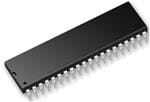
| 供应商器件封装 | 40-PDIP |
| 包装 | 管件 |
| 商标 | Microchip Technology |
| 安装类型 | 通孔 |
| 安装风格 | Through Hole |
| 封装 | Tube |
| 封装/外壳 | 40-DIP(0.600",15.24mm) |
| 封装/箱体 | PDIP-40 |
| 工作温度 | 0°C ~ 70°C |
| 工作电源电压 | 9 V |
| 工厂包装数量 | 10 |
| 接口 | - |
| 数字或字符 | A/D,3.5 位数字 |
| 显示类型 | LCD |
| 最大功率耗散 | 1230 mW |
| 最大工作温度 | + 70 C |
| 最小工作温度 | 0 C |
| 标准包装 | 10 |
| 电压-电源 | 9V |
| 电流-电源 | 800µA |
| 配置 | 7 段显示 |


- 商务部:美国ITC正式对集成电路等产品启动337调查
- 曝三星4nm工艺存在良率问题 高通将骁龙8 Gen1或转产台积电
- 太阳诱电将投资9.5亿元在常州建新厂生产MLCC 预计2023年完工
- 英特尔发布欧洲新工厂建设计划 深化IDM 2.0 战略
- 台积电先进制程称霸业界 有大客户加持明年业绩稳了
- 达到5530亿美元!SIA预计今年全球半导体销售额将创下新高
- 英特尔拟将自动驾驶子公司Mobileye上市 估值或超500亿美元
- 三星加码芯片和SET,合并消费电子和移动部门,撤换高东真等 CEO
- 三星电子宣布重大人事变动 还合并消费电子和移动部门
- 海关总署:前11个月进口集成电路产品价值2.52万亿元 增长14.8%


PDF Datasheet 数据手册内容提取
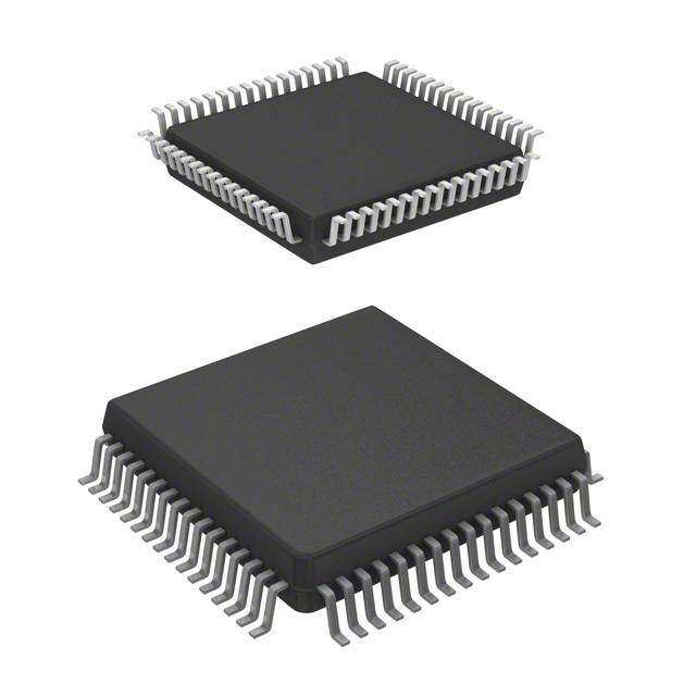
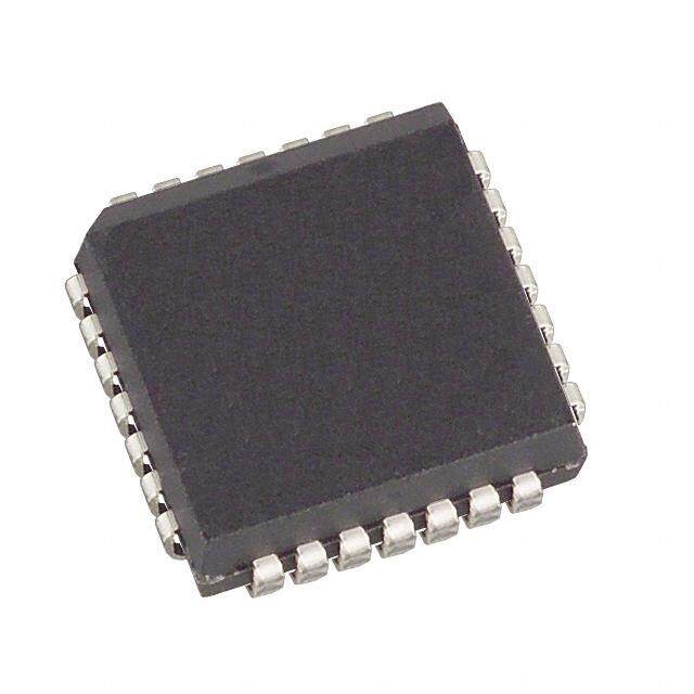
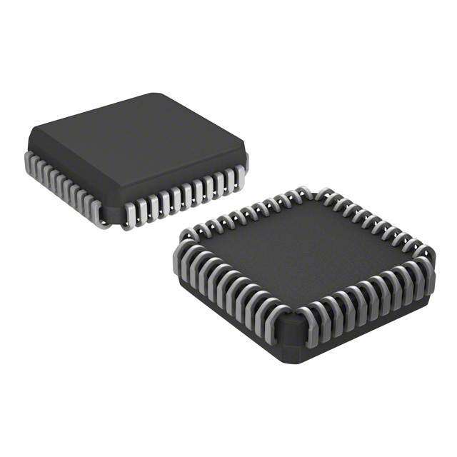
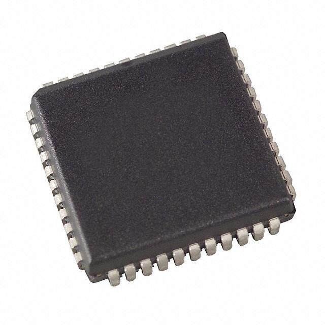
TC7116/A/TC7117/A 3-1/2 Digit Analog-to-Digital Converters with Hold Features General Description • LowTemperatureDriftInternalReference TheTC7116A/TC7117Aare3-1/2digitCMOSanalog- - TC7116/TC711780ppm/°CTyp. to-digital converters (ADCs) containing all the active componentsnecessarytoconstructa0.05%resolution - TC7116A/TC7117A20ppm/°CTyp. measurement system. Seven-segment decoders, (cid:127) DisplayHoldFunction polarity and digit drivers, voltage reference, andclock (cid:127) DirectlyDrivesLCDorLEDDisplay circuitareintegratedon-chip.TheTC7116Adrivesliq- (cid:127) ZeroReadingwithZeroInput uid crystal displays (LCDs) and includes a backplane (cid:127) LowNoiseforStableDisplay driver.TheTC7117Adrivescommonanodelightemit- - 2Vor200mVFullScaleRange(FSR) ting diode (LED) displays directly with an 8mA drive currentpersegment. (cid:127) Auto-ZeroCycleEliminatesNeedforZero Thesedevicesincorporateadisplayhold(HLDR)func- (cid:127) AdjustmentPotentiometer tion. The displayed reading remains indefinitely, as (cid:127) TruePolarityIndicationforPrecisionNull longasHLDRisheldhigh.Conversionscontinue,but Applications outputdatadisplaylatchesarenotupdated.Therefer- (cid:127) Convenient9VBatteryOperation: encelowinput(V -)isnotavailable,asitiswiththe REF (TC7116/TC7116A) TC7106/7107. V -is tied internally to analog com- REF (cid:127) HighImpedanceCMOSDifferentialInputs:10 12Ω monintheTC7116A/7117Adevices. (cid:127) LowPowerOperation:10mW The TC7116A/7117A reduces linearity error to less than1count.Rollovererror(thedifferenceinreadings Applications forequalmagnitudebutoppositepolarityinputsignals) (cid:127) Thermometry is below ±1 count. High-impedance differential inputs offer 1pA leakage current and a 1012Ω input imped- (cid:127) BridgeReadouts: StrainGauges,LoadCells, ance.The15µV noiseperformanceenablesa“rock NullDetectors P-P solid”reading.Theauto-zerocycleensuresazerodis- (cid:127) DigitalMeters: Voltage/Current/Ohms/Power,pH playreadingwitha0Vinput. (cid:127) DigitalScales,ProcessMonitors The TC7116A and TC7117A feature a precision, low (cid:127) PortableInstrumentation driftinternalreference,andarefunctionallyidenticalto the TC7116/TC7117. A low drift external reference is Device Selection Table notnormallyrequiredwiththeTC7116A/TC7117A. PackageCode Package TemperatureRange CPL 40-PinPDIP 0°Cto+70°C IJL 40-PinCERDIP -25°Cto+85°C CKW 44-PinPQFP 0°Cto+70°C CLW 44-PinPLCC 0°Cto+70°C 2002MicrochipTechnologyInc. DS21457B-page 1
TC7116/A/TC7117/A Package Type 40-Pin PDIP 40-Pin CERDIP HLDR 1 40 OSC1 HLDR 1 40 OSC1 D1 2 39 OSC2 D1 2 39 OSC2 C1 3 38 OSC3 C1 3 38 OSC3 B1 4 37 TEST B1 4 37 TEST 1's A1 5 36 VREF+ 1's A1 5 36 VREF+ F1 6 35 V+ F1 6 35 V+ G1 7 34 CREF+ G1 7 34 CREF+ E1 8 TC7116CPL 33 CREF- E1 8 33 CREF- D2 9 TC7116ACPL 32 COMMON D2 9 TC7116IJL 32 COMMON C2 10 TC7117CPL 31 VIN+ C2 10 TC7116AIJL 31 VIN+ TC7117ACPL TC7117IJL 10's B2 11 30 VIN- 10's B2 11 TC7117AIJL 30 VIN- A2 12 29 CAZ A2 12 29 CAZ F2 13 28 VBUFF F2 13 28 VBUFF E2 14 27 VINT E2 14 27 VINT D3 15 26 V- D3 15 26 V- 100's B3 16 25 G2 100's B3 16 25 G2 F3 17 24 C3 100's F3 17 24 C3 100's E3 18 23 A3 E3 18 23 A3 1000's AB4 19 22 G3 1000's AB4 19 22 G3 POL 20 21 BP/GND POL 20 21 BP/GND (Minus Sign) (TC7116/7117) (Minus Sign) (TC7116/7117) (TC7116A/TC7117A) (TC7116A/TC7117A) 44-Pin PLCC 44-Pin PQFP N O A1 B1C1 D1 HLDR NC OSC1 OSC2 OSC3 TEST V+REF V+REF V+ C+REF C-REF COMM V+IN V-IN CAZ VBUFF VINT V- 6 5 4 3 2 1 44 43 42 41 40 44 43 42 41 40 39 38 37 36 35 34 F1 7 39V+ NC 1 33NC G1 8 38 CREF+ NC 2 32G3 E1 9 37 CREF- TEST3 31C3 D210 36COMMON OSC3 4 30A3 C211 TC7116CLW 35VIN+ NC 5 TC7116CKW 29G3 NC12 TC7116ACLW 34NC OSC2 6 TC7116ACKW 28BGPN/D B213 TC7117CLW 33VIN- OSC1 7 TC7117CKW 27POL A2 14 TC7117ACLW 32CAZ HLDR 8 TC7117ACKW 26AB4 F215 31VBUFF D1 9 25E3 E2 16 30VINT C110 24F3 D317 29V- B1 11 23B3 18 19 20 21 22 23 24 25 26 27 28 12 13 14 15 16 17 18 19 20 21 22 B3F3 E3AB4 POL NCBP/GNDG3 A3 C3 G2 A1 F1 G1 E1 D2 C2 B2 A2 F2 E2 D3 Note 1: NC=Nointernalconnection. 2: Pins9,25,40and56areconnectedtothediesubstrate.ThepotentialatthesepinsisapproximatelyV+.Noexternal connectionsshouldbemade. DS21457B-page 2 2002MicrochipTechnologyInc.
TC7116/A/TC7117/A TypicalApplication TC7116/A TC7117/A Display 0.1µF Hold LCD Display (TC7116/7116A) 34 33 1 or Common Anode LED Display (TC7117/7117A) 1MΩ CREF+ CREF-HLDR + 31 VIN+ 222––1295 SDerigvement Analog 0.01µF I–nput 30 VIN- POL 20Minus Sign Backplane Drive BP/GND 21 32 ANALOG COMMON V+ 35 24kΩ 28 VBUFF + 47kΩ 0.47µF 36 VREF 9V 29 CAZ VREF+ 100mV 1kΩ 0.22µF 27 VINT V- 26 OSC2 OSC3 OSC1 To Analog 39 38 COSC 40 Common (Pin 32) ROSC 100pF 3 Conversions Per Second 100kΩ 2002MicrochipTechnologyInc. DS21457B-page 3
TC7116/A/TC7117/A 1.0 ELECTRICAL *Stresses above those listed under "Absolute Maximum Ratings"maycausepermanentdamagetothedevice.These CHARACTERISTICS arestressratingsonlyandfunctionaloperationofthedevice attheseoranyotherconditionsabovethoseindicatedinthe Absolute Maximum Ratings* operation sections of the specifications is not implied. Exposure to Absolute Maximum Rating conditions for SupplyVoltage: extendedperiodsmayaffectdevicereliability. TC7116/TC7116A(V+toV-)...........................15V TC7117/TC7117A(V+toGND).......................+6V V-toGND.........................................................-9V AnalogInputVoltage(EitherInput)(Note1)...V+toV- ReferenceInputVoltage(EitherInput)............V+toV- ClockInput: TC7116/TC7116A...............................TESTtoV+ TC7117/TC7117A.................................GNDtoV+ PackagePowerDissipation;T ≤70°C(Note2) A 40-PinCDIP................................................2.29W 40-PinPDIP................................................1.23W 44-PinPLCC...............................................1.23W 44-PinPQFP...............................................1.00W OperatingTemperature: C(Commercial)Device................... 0°Cto+70°C I (Commercial)Device.................... 0°Cto+70°C StorageTemperature..........................-65°Cto+150°C TC7116/AANDTC7117/AELECTRICALSPECIFICATIONS ElectricalCharacteristics:Unlessotherwisenoted,specificationsapplytoboththeTC7116/AandTC7117/AatT =25°C, A f =48kHz.PartsaretestedinthecircuitoftheTypicalOperatingCircuit. CLOCK Symbol Parameter Min Typ Max Unit TestConditions Z ZeroInputReading — ±0 — Digital V =0V IR IN Reading FullScale=200mV RatiometricReading 999 999/1000 1000 Digital V =V IN REF Reading V =100mV REF R/O RolloverError(DifferenceinReadingfor -1 ±0.2 +1 Counts V -=+V + ≅ 200mV IN IN EqualPositiveandNegative or≈ 2V ReadingsNearFullScale) Linearity(MaximumDeviationfromBest -1 ±0.2 +1 Counts FullScale=200mVor2V StraightLineFit) CMRR CommonModeRejectionRatio — 50 — µV/V V =±1V,V =0V CM IN (Note3) FullScale=200mV e Noise(PeaktoPeak95%ofTime) — 15 — µV V =0V N IN FullScale=200mV I LeakageCurrentatInput — 1 10 pA V =0V L IN ZeroReadingDrift — 0.2 1 µV/°C V =0V IN “C”Device=0°Cto+70°C — 1.0 2 µV/°C “I”Device=-25°Cto+85°C Note 1: Inputvoltagesmayexceedthesupplyvoltagesprovidedtheinputcurrentislimitedto±100µA. 2: Dissipationratingassumesdeviceismountedwithallleadssolderedtoprintedcircuitboard. 3: Referto“DifferentialInput”discussion. 4: Backplanedriveisinphasewithsegmentdrivefor“OFF”segment,180°outofphasefor“ON”segment.Frequencyis 20timesconversionrate.AverageDCcomponentislessthan50mV. 5: TheTC7116/TC7116Alogicinputshaveaninternalpull-downresistorconnectedfromHLDR,Pin1toTEST,Pin37.The TC7117/TC7117Alogicinputshaveaninternalpull-downresistorconnectedfromHLDR,Pin1toGND,Pin21. DS21457B-page 4 2002MicrochipTechnologyInc.
TC7116/A/TC7117/A TC7116/AANDTC7117/AELECTRICALSPECIFICATIONS(CONTINUED) ElectricalCharacteristics:Unlessotherwisenoted,specificationsapplytoboththeTC7116/AandTC7117/AatT =25°C, A f =48kHz.PartsaretestedinthecircuitoftheTypicalOperatingCircuit. CLOCK Symbol Parameter Min Typ Max Unit TestConditions TC ScaleFactorTemperatureCoefficient — 1 5 ppm/°C V =199mV, SF IN “C”Device=0°Cto+70°C (Ext.Ref=0ppm°C) — — 20 ppm/°C “I”Device=-25°Cto+85°C InputResistance,Pin1 30 70 — kΩ (Note5) V Pin1 — — Test+1.5 V TC7116/AOnly IL, V Pin1 — — GND+1.5 V TC7117/AOnly IL, V Pin1 V+-1.5 — — V Both IH, I SupplyCurrent(DoesnotIncludeLED — 0.8 1.8 mA V =0V DD IN CurrentforTC7117/A) V AnalogCommonVoltage 2.4 3.05 3.35 V 25kΩBetweenCommon C (withRespecttoPositiveSupply) andPositiveSupply V TemperatureCoefficientofAnalog — — — — “C”Device:0°Cto +70°C CTC Common(withRespecttoPositive 20 50 ppm/°C TC7116A/TC7117A Supply) 80 — ppm/°C TC7116/TC7117 V TC7116/TC7117AONLYPeaktoPeak 4 5 6 V V+toV-=9V SD SegmentDriveVoltage (Note4) V TC7116A/TC7116AONLYPeaktoPeak 4 5 6 V V+toV-=9V BD BackplaneDriveVoltage (Note4) TC7117/TC7117AONLY 5 8 — mA V+=5.0V SegmentSinkingCurrent SegmentVoltage=3V (ExceptPin19) TC7117/TC7117AONLY 10 16 — mA V+=5.0V SegmentSinkingCurrent(Pin19Only) SegmentVoltage=3V Note 1: Inputvoltagesmayexceedthesupplyvoltagesprovidedtheinputcurrentislimitedto±100µA. 2: Dissipationratingassumesdeviceismountedwithallleadssolderedtoprintedcircuitboard. 3: Referto“DifferentialInput”discussion. 4: Backplanedriveisinphasewithsegmentdrivefor“OFF”segment,180°outofphasefor“ON”segment.Frequencyis 20timesconversionrate.AverageDCcomponentislessthan50mV. 5: TheTC7116/TC7116Alogicinputshaveaninternalpull-downresistorconnectedfromHLDR,Pin1toTEST,Pin37.The TC7117/TC7117Alogicinputshaveaninternalpull-downresistorconnectedfromHLDR,Pin1toGND,Pin21. 2002MicrochipTechnologyInc. DS21457B-page 5
TC7116/A/TC7117/A 2.0 PIN DESCRIPTIONS ThedescriptionsofthepinsarelistedinTable2-1. TABLE 2-1: PINFUNCTIONTABLE PinNumber PinNumber (40-PinPDIP) Symbol Description (44-PinPQFP) (40-PinCERDIP) 1 8 HLDR Holdpin,Logic1holdspresentdisplayreading. 2 9 D ActivatestheDsectionoftheunitsdisplay. 1 3 10 C ActivatestheCsectionoftheunitsdisplay. 1 4 11 B ActivatestheBsectionoftheunitsdisplay. 1 5 12 A ActivatestheAsectionoftheunitsdisplay. 1 6 13 F ActivatestheFsectionoftheunitsdisplay. 1 7 14 G ActivatestheGsectionoftheunitsdisplay. 1 8 15 E ActivatestheEsectionoftheunitsdisplay. 1 9 16 D ActivatestheDsectionofthetensdisplay. 2 10 17 C ActivatestheCsectionofthetensdisplay. 2 11 18 B ActivatestheBsectionofthetensdisplay. 2 12 19 A ActivatestheAsectionofthetensdisplay. 2 13 20 F ActivatestheFsectionofthetensdisplay. 2 14 21 E ActivatestheEsectionofthetensdisplay. 2 15 22 D ActivatestheDsectionofthehundredsdisplay. 3 16 23 B ActivatestheBsectionofthehundredsdisplay. 3 17 24 F ActivatestheFsectionofthehundredsdisplay. 3 18 25 E ActivatestheEsectionofthehundredsdisplay. 3 19 26 AB Activatesbothhalvesofthe1inthethousandsdisplay. 4 20 27 POL Activatesthenegativepolaritydisplay. 21 28 BP/ LCDbackplanedriveoutput(TC7116/TC7116A).Digitalground GND (TC7117/TC7117A). 22 29 G ActivatestheGsectionofthehundredsdisplay. 3 23 30 A ActivatestheAsectionofthehundredsdisplay. 3 24 31 C ActivatestheCsectionofthehundredsdisplay. 3 25 32 G ActivatestheGsectionofthetensdisplay. 2 26 34 V- Negativepowersupplyvoltage. 27 35 V Integratoroutput.Connectionpointforintegrationcapacitor. INT SeeSection4.3,IntegratingCapacitorformoredetails. 28 36 V Integrationresistorconnection.Usea47kΩresistorfora200mVfullscalerange BUFF anda470kΩresistorfor2Vfullscalerange. 29 37 C Thesizeoftheauto-zerocapacitorinfluencessystemnoise.Usea0.47µF AZ capacitorfor200mVfullscale,anda0.047µFcapacitorfor2Vfullscale. SeeSection4.1,Auto-ZeroCapacitorformoredetails. 30 38 V - TheanalogLOWinputisconnectedtothispin. IN 31 39 V + TheanalogHIGHinputsignalisconnectedtothispin. IN 32 40 COMMON ThispinisprimarilyusedtosettheAnalogCommonmodevoltageforbattery operation,orinsystemswheretheinputsignalisreferencedtothepowersupply. Italsoactsasareferencevoltagesource.SeeSection3.1.6,AnalogCommon formoredetails. 33 41 C - SeePin34. REF 34 42 C + A0.1µFcapacitorisusedinmostapplications.IfalargeCommonmodevoltage REF exists(forexample,theV -pinisnotatanalogcommon),anda200mVscaleis IN used,a1µFcapacitorisrecommendedandwillholdtherollovererrorto 0.5count. DS21457B-page 6 2002MicrochipTechnologyInc.
TC7116/A/TC7117/A TABLE 2-1: PINFUNCTIONTABLE(CONTINUED) PinNumber PinNumber (40-PinPDIP) Symbol Description (44-PinPQFP) (40-PinCERDIP) 35 43 V+ PositivePowerSupplyVoltage. 36 44 V + Theanaloginputrequiredtogenerateafullscaleoutput(1999counts).Place REF 100mVbetweenPins32and36for199.9mVfullscale.Place1Vbetween Pins35and36for2Vfullscale.SeeSection4.6,ReferenceVoltage. 37 3 TEST Lamptest.WhenpulledHIGH(toV+),allsegmentswillbeturnedonandthedis- playshouldread-1888.Itmayalsobeusedasanegativesupplyforexternally generateddecimalpoints.SeeSection3.1.7,TESTforadditionalinformation. 38 4 OSC3 SeePin40. 39 6 OSC2 SeePin40. 40 7 OSC1 Pins40,39,38makeuptheoscillatorsection.Fora48kHzclock(3readingsper section),connectPin40tothejunctionofa100kΩresistoranda100pFcapaci- tor.The100kΩresistoristiedtoPin39andthe100pFcapacitoristiedtoPin38. 3.0 DETAILED DESCRIPTION 3.1.2 SIGNALINTEGRATE PHASE (AllPinDesignationsReferto40-PinPDIP.) The auto-zero loop is opened, the internal short is removed,andtheinternalhighandlowinputsarecon- 3.1 Analog Section nected to the external pins. The converter then inte- gratesthedifferential voltagesbetweenV +andV - IN IN Figure3-1showstheblockdiagramoftheanalogsec- forafixedtime.Thisdifferentialvoltagecanbewithina tion for the TC7116/TC7116A and TC7117/TC7117A. wideCommonmoderange: 1Vofeither supply. How- Eachmeasurementcycleisdividedintothreephases: ever,iftheinputsignalhasnoreturnwithrespecttothe (1) Auto-Zero (AZ), (2) Signal Integrate (INT), and converter power supply, V - can be tied to analog IN (3)ReferenceIntegrate(REF),orDe-integrate(DE). common to establish the correct Common mode volt- age. At the end of this phase, the polarity of the 3.1.1 AUTO-ZEROPHASE integratedsignalisdetermined. Highandlowinputsaredisconnectedfromthepinsand internally shorted to analog common. The reference capacitor is charged to the referencevoltage. A feed- back loop is closed around the system to charge the auto-zerocapacitor(C )tocompensateforoffsetvolt- AZ agesinthebufferamplifier,integrator,andcomparator. Sincethecomparatorisincludedintheloop,AZaccu- racyislimitedonlybysystemnoise.Theoffsetreferred totheinputislessthan10µV. 2002MicrochipTechnologyInc. DS21457B-page 7
TC7116/A/TC7117/A FIGURE3-1: ANALOGSECTIONOFTC7116/TC7117AANDTC7117/TC7117A CREF RINT CAZ CINT CREF+ VREF+ CREF- VBUFF V+ Auto-Zero VINT V+ 34 36 33 28 35 29 27 – Integrator 10µA AZ + Low – 31 Temp. + To VIN+ Drift + Digital DE DE Section INT (–) (+) Zener AZ – VREF AZ Comparator + 32 DE (+) DE (–) TC7116 Analog Common V+ -3V TC7116A 30 AZ & DE (±) TC7117 VIN- TC7117A INT 26 V- 3.1.3 REFERENCE INTEGRATE PHASE 3.1.6 ANALOGCOMMON Thefinalphaseisreferenceintegrate,orde-integrate. ThispinisincludedprimarilytosettheCommonmode Input low is internally connected to analog common voltageforbatteryoperation(TC7116/TC7116A),orfor and input high is connected across the previously any system where the input signals are floating, with charged reference capacitor. Circuitry within the chip respect to the power supply. The analog common pin ensures that the capacitor will be connected with the setsavoltageapproximately2.8Vmorenegativethan correctpolaritytocausetheintegratoroutputtoreturn thepositivesupply.Thisisselectedtogiveaminimum to zero. The time required for the output to return to endoflifebatteryvoltageofabout6V.However,analog zero is proportional to the input signal. The digital common has some attributes of a reference voltage. readingdisplayedis: Whenthetotalsupplyvoltageislargeenoughtocause the zener to regulate (>7V), the analog common volt- EQUATION3-1: age will have a low voltage coefficient (0.001%), low 1000= VIN output impedance (≅15Ω), and a temperature coeffi- VREF cientoflessthan20ppm/°C,typically,and50ppmmax- imum. The TC7116/TC7117 temperature coefficients 3.1.4 REFERENCE aretypically80ppm/°C. An external reference may be used, if necessary, as The positive reference voltage (V +) is referred to REF showninFigure3-2. analogcommon. 3.1.5 DIFFERENTIALINPUT FIGURE3-2: USINGANEXTERNAL REFERENCE This input can accept differential voltages anywhere within the Common mode range of theinput amplifier V+ or,specifically,from1Vbelowthepositivesupplyto1V above the negative supply. In this range, the system hasaCMRRof86dB,typical.However,sincetheinte- V+ grator also swings with the Common mode voltage, TC7116 6.8kΩ care must be exercised to ensure that the integrator TC7116A outputdoesnotsaturate.Aworstcaseconditionwould TC7117 bealarge,positiveCommonmodevoltagewithanear TC7117A fullscalenegativedifferentialinputvoltage.Thenega- 20kΩ tive input signal drives the integrator positive, when VREF+ most of its swing has been used up by the positive 1.2V REF Commonmodevoltage.Forthesecriticalapplications, COMMON the integrator swing can be reduced to less than the recommended 2V full scale swing with little loss of accuracy. Theintegrator output canswingwithin0.3V ofeithersupplywithoutlossoflinearity. DS21457B-page 8 2002MicrochipTechnologyInc.
TC7116/A/TC7117/A Analog common is also used as V - return during FIGURE3-4: EXCLUSIVE“OR”GATE IN auto-zeroandde-integrate.IfVIN-isdifferentfromana- FORDECIMALPOINT log common, a Common mode voltage exists in the DRIVE systemandistakencareofbytheexcellentCMRRof theconverter.However,insomeapplications,VIN-will V+ besetatafixed,knownvoltage(powersupplycommon V+ for instance). In this application, analog common BP should be tied to the same point, thus removing the Common mode voltagefrom theconverter. Thesame TC7116 To LCD holdstrueforthereferencevoltage;ifitcanbeconve- TC7116A Decimal Decimal Point niently referenced to analog common, it should be. Select Point This removes the Common mode voltage from the referencesystem. 4030 WithintheIC, analogcommonistiedtoanN-channel TEST GND FET,thatcansink30mAormoreofcurrenttoholdthe voltage 3V below the positive supply (when a load is trying to pull the analog common line positive). How- 3.2 Digital Section ever, there is only 10µA of source current, so analog commonmayeasilybetiedtoamorenegativevoltage, Figure3-5 and Figure3-6 show the digital section for thusoverridingtheinternalreference. TC7116/TC7116AandTC7117/TC7117A,respectively. FortheTC7116/TC7116A(Figure3-5),aninternaldig- 3.1.7 TEST ital ground isgenerated from a 6V zener diode and a large P-channel source follower. This supply is made The TEST pin serves two functions. On the TC7117/ stiff to absorb the relative large capacitive currents TC7117A,itiscoupledtotheinternallygenerateddigi- talsupplythrougha500Ωresistor.Thus,itcanbeused whenthebackplane(BP)voltageisswitched.TheBP asanegativesupplyforexternallygeneratedsegment frequencyistheclockfrequency4800.For3readings drivers,suchasdecimalpoints,oranyotherpresenta- persecond,thisisa60Hzsquarewavewithanominal amplitudeof5V.Thesegmentsaredrivenatthesame tion the user may want to include on the LCD. frequency and amplitude, and are in phase with BP (Figure3-3and Figure3-4showsuchanapplication.) when OFF, but out of phase when ON. In all cases, Nomorethana1mAloadshouldbeapplied. negligibleDCvoltageexistsacrossthesegments. The second function is a "lamp test." When TEST is pulled HIGH (to V+), all segments will be turned ON Figure3-6 is the digital section of the TC7117/ TC7117A. It is identical to the TC7116/TC7116A, and thedisplay should read -1888. The TEST pinwill except that the regulated supply and BP drive have sinkabout10mAundertheseconditions. been eliminated, and the segment drive is typically 8mA.The1000'soutput(Pin19)sinkscurrentfromtwo FIGURE3-3: SIMPLEINVERTERFOR LED segments, and has a16mA drive capability. The FIXEDDECIMALPOINT TC7117/TC7117A are designed to drive common anodeLEDdisplays. V+ V+ Inbothdevices,thepolarityindicationisONforanalog inputs.IfV -andV +arereversed,thisindicationcan TC7116 4049 bereverseIdNalso,ifINdesired. TC7116A BP To LCD 21 Decimal Point GND TEST 37 To LCD Backplane 2002MicrochipTechnologyInc. DS21457B-page 9
TC7116/A/TC7117/A FIGURE3-5: TC7116/TC7116ADIGITALSECTION TC7116 TC7116A Backplane 21 LCD Phase Driver Typical Segment Output V+ 7-Segment 7-Segment 7-Segment ÷200 0.5mA Decode Decode Decode Segment Output 2mA Latch Internal Digital Ground Thousands Hundreds Tens Units To Switch Drivers From Comparator Output 35 V+ Clock ~70kΩ 6.2V ÷4 Logic Control 37 TEST VTH = 1V 500Ω 40 39 38 Internal Digital Ground 1 26 V- OSC1 OSC2 OSC3 HLDR 3.2.1 SYSTEMTIMING Toachievemaximumrejectionof60Hzpickup,thesig- nalintegratecycleshouldbeamultipleof60Hz.Oscil- The clocking method used for the TC7116/TC7116A lator frequencies of 240kHz, 120kHz, 80kHz, 60kHz, and TC7117/TC7117A is shown in Figure3-6. Three 48kHz,40kHz,etc.shouldbeselected.For50Hzrejec- clockingmethodsmaybeused: tion, oscillator frequencies of 200kHz, 100kHz, 1. AnexternaloscillatorconnectedtoPin40. 66-2/3kHz,50kHz,40kHz,etc.wouldbesuitable.Note 2. AcrystalbetweenPins39and40. that 40kHz (2.5 readings per second) will reject both 50Hzand60Hz. 3. AnRCnetworkusingallthreepins. The oscillator frequency is ÷4 before it clocks the 3.2.2 HOLDREADINGINPUT decade counters. It is then further divided to form the When HLDR is at a logic HIGH, the latch will not be three convert cycle phases: Signal Integrate (1000 counts), Reference De-integrate (0 to 2000 counts), updated. Analog-to-digital conversions will continue, andAuto-Zero(1000to3000counts).Forsignalsless butwillnotbeupdateduntilHLDRisreturnedtoLOW. thanfullscale,auto-zerogetstheunusedportionofref- To continuously update the display, connect to TEST (TC7116/TC7116A) or GROUND (TC7117/TC7117A), erencede-integrate. This makes acomplete measure or disconnect. This input is CMOS compatible with cycle of 4000 (16,000 clock pulses), independent of 70kΩtypicalresistancetoTEST(TC7116/TC7116A)or inputvoltage.For3readingsper second,anoscillator frequencyof48kHzwouldbeused. GROUND(TC7117/TC7117A). DS21457B-page 10 2002MicrochipTechnologyInc.
TC7116/A/TC7117/A FIGURE3-6: TC7117/TC711ADIGITALSECTION TC7117 TC7117A Typical Segment Output V+ 7-Segment 7-Segment 7-Segment 0.5mA Decode Decode Decode To Segment 8mA Latch Digital Ground Internal Digital Ground Thousands Hundreds Tens Units To Switch Drivers From Comparator Output V+ 35 V+ 37 Clock TEST ÷4 Control Logic 500Ω 21 Digital GND 40 39 38 1 ~70kΩ OSC1 OSC2 OSC3 HLDR 2002MicrochipTechnologyInc. DS21457B-page11
TC7116/A/TC7117/A 4.0 COMPONENT VALUE 4.6 Reference Voltage SELECTION Togeneratefullscaleoutput(2000counts),theanalog inputrequirementisV =2V .Thus,forthe200mV IN REF 4.1 Auto-Zero Capacitor and 2V scale, V should equal 100mV and 1V, REF respectively. In many applications, where the ADC is Thesizeoftheauto-zerocapacitorhassomeinfluence connected to a transducer, a scale factor exists onsystemnoise.For200mVfullscale,wherenoiseis very important, a 0.47µF capacitor is recommended. between the input voltage and the digital reading. For On the 2V scale, a 0.047µF capacitor increases the instance,inameasuringsystem,thedesignermightlike tohaveafull scalereadingwhenthe voltagefrom the speed of recovery from overload and is adequate for transduceris700mV.Insteadofdividingtheinputdown noiseonthisscale. to 200mV, the designer should use the input voltage 4.2 Reference Capacitor directly and select VREF=350mV. Suitable values for integratingresistorandcapacitorwouldbe120kWand A 0.1µF capacitor is acceptable in most applications. 0.22µF.Thismakesthesystemslightlyquieterandalso However,wherealargeCommonmodevoltageexists avoids a divider network on the input. The TC7117/ (i.e., the VIN- pin is not at analog common), and a TC7117A, with ±5V supplies, can accept input signals 200mVscaleisused,alargervalueisrequiredtopre- upto±4V.Anotheradvantageofthissystemiswhena ventrollovererror.Generally,1µFwillholdtherollover digital readingof zeroisdesiredfor V ≠0. Tempera- IN errorto0.5countinthisinstance. ture and weighing systems with a variable tare are examples.Thisoffsetreadingcanbeconvenientlygen- 4.3 Integrating Capacitor erated by connecting the voltage transducer between V + and analog common, and the variable (or fixed) Theintegratingcapacitorshouldbeselectedtogivethe IN offsetvoltagebetweenanalogcommonandV -. maximumvoltageswingthatensurestolerancebuildup IN will not saturate the integrator swing (approximately 0.3V from either supply). In the TC7116/TC7116A or 5.0 TC7117/TC7117A POWER the TC7117/TC7117A, when the analog common is SUPPLIES usedasareference,anominal±2Vfullscaleintegrator swing is acceptable. For the TC7117/TC7117A, with The TC7117/TC7117A are designed to operate from ±5V supplies and analog common tied to supply ±5Vsupplies.However,ifanegativesupplyisnotavail- ground, a ±3.5V to±4Vswing is nominal. For 3 read- able,itcanbegeneratedwithaTC7660DC-to-DCcon- ingspersecond(48kHzclock),nominalvaluesforC verter and two capacitors. Figure5-1 shows this INT are0.22µ1Fand0.10µF,respectively.Ifdifferentoscil- application. lator frequencies are used, these values should be In selected applications, a negative supply is not changed in inverse proportion to maintain the output required.Theconditionsforusingasingle+5Vsupply swing.Theintegratingcapacitormusthavelowdielec- are: tricabsorptiontopreventrollovererrors.Polypropylene 1. Theinputsignalcanbereferencedtothecenter capacitorsarerecommendedforthisapplication. oftheCommonmoderangeoftheconverter. 4.4 Integrating Resistor 2. Thesignalislessthan±1.5V. 3. Anexternalreferenceisused. Boththebufferamplifierandtheintegratorhaveaclass A output stage with100µA of quiescent current. They FIGURE5-1: NEGATIVE POWER can supply 20µA of drive current with negligible non- SUPPLY GENERATION linearity. The integrating resistor should be large WITHTC7660 enough to remain in this very linear region over the inputvoltagerange,butsmallenoughthatundueleak- +5V agerequirementsarenotplacedonthePCboard.For 35 2V full scale, 470kΩ is near optimum and, similarly, V+ 36 47kΩfor200mVfullscale. VREF+ LED 4.5 OscillatorComponents Drive 32 TC7117 COM For all frequency ranges, a 100kΩ resistor is recom- TC7117AVIN+ 31 + mended;thecapacitorisselectedfromtheequation: 30 VIN 8 VIN- – EQUATION4-1: 2 21 + V- GND 10µF TC7660 0.45 26 f = ----------- 4 5 (-5V) RC 3 + Fora48kHzclock(3readingspersecond),C=100pF. 10µF DS21457B-page 12 2002MicrochipTechnologyInc.
TC7116/A/TC7117/A 6.0 TYPICAL APPLICATIONS Inadditiontolimitingmaximum power dissipation, the resistor reduces change in power dissipation as the The TC7117/TC7117A sink the LED display current, displaychanges.Theeffectiscausedbythefactthat, causingheattobuildupintheICpackage.Iftheinter- as fewer segments are ON, each ON output drops nal voltage reference is used, the changing chip tem- morevoltageandcurrent.Forthebestcaseofsixseg- peraturecan causethedisplaytochangereading.By ments(a“111”display)toworstcase(a“1888”display), reducingtheLEDcommonanodevoltage,theTC7117/ the resistor circuit will change about 230mW, while a TC7117Apackagepowerdissipationisreduced. circuit without the resistor will change about 470mW. Figure6-1 is a curve tracer display showing the rela- Therefore,theresistorwillreducetheeffect of display tionshipbetweenoutputcurrentandoutputvoltagefor dissipationonreferencevoltagedriftbyabout50%. typical TC7117CPL/TC7117ACPL devices. Since a ThechangeinLEDbrightnesscausedbytheresistoris typicalLEDhas1.8Vacrossitat8mAanditscommon almostunnoticeableasmoresegmentsturnoff.Ifdis- anodeisconnectedto+5V,theTC7117/TC7117Aout- play brightness remaining steady is very important to put is at 3.2V (Point A, Figure6-1). Maximum power the designer, a diode may be used instead of the dissipationis8.1mAx3.2Vx24segments=622mW. resistor. However,noticethatoncetheTC7117/TC7117A'sout- putvoltageisabove2V,theLEDcurrentisessentially FIGURE6-2: DIODE ORRESISTOR constant as output voltage increases. Reducing the LIMITSPACKAGEPOWER output voltage by0.7V (Point B Figure6-1) resultsin DISSIPATION 7.7mAofLEDcurrent,onlya5%reduction.Maximum power dissipation is now only 7.7mA x 2.5V x 24 = +5V + In – -5V 462mW,areductionof26%.Anoutputvoltagereduc- tion of 1V (Point C) reduces LED current by 10% 24kΩ 1MΩ 150kΩ (7.3mA), but powerdissipationby38%(7.3mAx2.2V TP3 1kΩ x24=385mW). 1p0F0 0µ.0F1 0µ.4F7 0.µ2F2 TP5 FIGURE6-1: TC7117/TC7117AOUTPUT TP2 0.1 Display VS.OUTPUTVOLTAGE 1k0Ω0 TP1 µF k4Ω7 40 35 30 TP 21 10.000 4 TC7117 TC7117A 1 10 20 A) 9.000 m ( A nt Display urre 8.000 B 1.5W, 1/4Ω C C ut 1N4001 p ut 7.000 O 6.000 2.00 2.50 3.00 3.50 4.00 OutputVoltage(V) Reduced power dissipation is very easy to obtain. Figure6-2showstwoways:eithera5.1Ω,1/4Wresis- tor,ora1Adiodeplacedinserieswiththedisplay(but not in series with the TC7117/TC7117A). The resistor reduces the TC7117/TC7117A's output voltage (when all24segmentsareON)toPointCofFigure6-1.When segmentsturnoff,theoutputvoltagewillincrease.The diode,however,willresultinarelativelysteadyoutput voltage,aroundPointB. 2002MicrochipTechnologyInc. DS21457B-page13
TC7116/A/TC7117/A FIGURE6-3: TC7116/TC7117AUSINGTHE INTERNALREFERENCE (200mVFULLSCALE,3READINGSPERSECOND-RPS) Set VREF = 100mV 40 100kΩ 39 38 37 100pF 36 22kΩ 35 34 0.1pF 1kΩ 33 1MΩ + 32 TC7116 31 0.01µF In TC7116A 30 0.47µF + – 29 47kΩ 28 9V 27 0.22µF – 26 25 24 To Display 23 22 21 To Backplane FIGURE6-4: TC7117/TC7117AINTERNALREFERENCE (200mVFULLSCALE,3RPS, V -TIEDTOGNDFORSINGLEENDEDINPUTS) IN Set VREF = 100mV 40 100kΩ 39 38 37 100pF 36 22kΩ 35 +5V 34 0.1pF 1kΩ 33 1MΩ + 32 31 0.01µF In TC7117 30 TC7117A 29 0.47µF 47kΩ – 28 27 0.22µF 26 -5V 25 24 To Display 23 22 21 DS21457B-page 14 2002MicrochipTechnologyInc.
TC7116/A/TC7117/A FIGURE6-5: CIRCUITFORDEVELOPINGUNDERRANGEANDOVERRANGE SIGNALS FROMTC7116/TC7117AOUTPUTS V+ 40 To Logic VCC 35 To Logic GND TC7116 TC7116A 26 V- O/R U/R 20 21 CD4023 or 74C10 CD4077 O/R = Over Range U/R = Under Range FIGURE6-6: TC7117/TC7117AWITHA1.2EXTERNALBANDGAPREFERENCE (V -TIEDTOCOMMON) IN 40 39 100kΩ Set VREF = 100mV 38 37 100pF 36 10kΩ 10kΩ 35 V+ 34 0.1pF 1kΩ 33 1.2V + 32 TC7117 31 0.01µF 1MΩ In TC7117A 2390 0.47µF 47kΩ – 28 27 0.22µF 26 25 24 To Display 23 22 21 2002MicrochipTechnologyInc. DS21457B-page15
TC7116/A/TC7117/A FIGURE6-7: RECOMMENDEDCOMPONENTVALUESFOR2VFULLSCALE (TC7116/TC7116AANDTC7117/TC7117A) Set VREF = 1V 40 100kΩ 39 38 37 100pF 36 24kΩ 35 V+ 34 0.1µF 25kΩ 33 1MΩ + 32 TC7116 31 0.01µF In TC7116A 30 0.047µF – TC7117 29 470kΩ 28 TC7117A 27 0.22µF 26 V- 25 24 To Display 23 22 21 FIGURE6-8: TC7117/TC7117AOPERATEDFROMSINGLE+5V SUPPLY (ANEXTERNALREFERENCEMUSTBEUSEDINTHISAPPLICATION) 40 39 100kΩ Set VREF = 100mV 38 37 100pF 36 10kΩ 10kΩ 35 V+ 34 0.1pF 1kΩ 33 1.2V + 32 TC7117 31 0.01µF 1MΩ In TC7117A 2390 0.47µF 47kΩ – 28 27 0.22µF 26 25 24 To Display 23 22 21 DS21457B-page 16 2002MicrochipTechnologyInc.
TC7116/A/TC7117/A 7.0 PACKAGING INFORMATION 7.1 Package Marking Information Packagemarkingdatanotavailableatthistime. 7.2 Taping Form Component Taping Orientation for 44-Pin PLCC Devices User Direction of Feed PIN 1 W P Standard Reel Component Orientation for TR Suffix Device Carrier Tape, Number of Components Per Reel and Reel Size Package Carrier Width (W) Pitch (P) Part Per Full Reel Reel Size 44-Pin PLCC 32 mm 24 mm 500 13 in Note: Drawing does not represent total number of pins. Component Taping Orientation for 44-Pin PQFP Devices User Direction of Feed PIN 1 W P Standard Reel Component Orientation for TR Suffix Device Carrier Tape, Number of Components Per Reel and Reel Size Package Carrier Width (W) Pitch (P) Part Per Full Reel Reel Size 44-Pin PQFP 24 mm 16 mm 500 13 in Note: Drawing does not represent total number of pins. 2002MicrochipTechnologyInc. DS21457B-page17
TC7116/A/TC7117/A 7.3 Package Dimensions 40-Pin PDIP (Wide) PIN 1 .555 (14.10) .530 (13.46) 2.065 (52.45) .610 (15.49) 2.027 (51.49) .590 (14.99) .200 (5.08) .140 (3.56) .040 (1.02) .020 (0.51) .015 (0.38) .150 (3.81) 3° MIN. .008 (0.20) .115 (2.92) .700 (17.78) .610 (15.50) .110 (2.79) .070 (1.78) .022 (0.56) .090 (2.29) .045 (1.14) .015 (0.38) Dimensions:inches(mm) 40-Pin CERDIP (Wide) PIN 1 .540 (13.72) .510 (12.95) .098 (2.49) MAX. .030 (0.76) MIN. 2.070 (52.58) .620 (15.75) 2.030 (51.56) .590 (15.00) .060 (1.52) .210 (5.33) .020 (0.51) .170 (4.32) .015 (0.38) .200 (5.08) .150 (3.81) .008 (0.20) 3° MIN. .125 (3.18) MIN. .700 (17.78) .620 (15.75) .110 (2.79) .065 (1.65) .020 (0.51) .090 (2.29) .045 (1.14) .016 (0.41) Dimensions:inches(mm) DS21457B-page 18 2002MicrochipTechnologyInc.
TC7116/A/TC7117/A 7.3 Package Dimensions (Continued) 44-Pin PLCC PIN 1 .050 (1.27) TYP. .021 (0.53) .013 (0.33) .695 (17.65) .685 (17.40) .630 (16.00) .591 (15.00) .656 (16.66) .650 (16.51) .032 (0.81) .026 (0.66) .020 (0.51) MIN. .656 (16.66) .650 (16.51) .120 (3.05) .695 (17.65) .090 (2.29) .685 (17.40) .180 (4.57) .165 (4.19) Dimenisons:inches(mm) 44-Pin PQFP 7° MAX. .009 (0.23) PIN 1 .005 (0.13) .041 (1.03) .026 (0.65) .018 (0.45) .012 (0.30) .398 (10.10) .390 (9.90) .557 (14.15) .031 (0.80) TYP. .537 (13.65) .010 (0.25) TYP. .398 (10.10) .390 (9.90) .083 (2.10) .075 (1.90) .557 (14.15) .537 (13.65) .096 (2.45) MAX. Dimenisons:inches(mm) 2002MicrochipTechnologyInc. DS21457B-page19
TC7116/A/TC7117/A PRODUCT IDENTIFICATION SYSTEM Toorderorobtaininformation,e.g.,onpricingordelivery,refertothefactoryorthelistedsalesoffice. PART CODE TC711X X X XXX 6 = LCD} 7 = LED A or blank* R (reversed pins) or blank (CPL pkg only) * "A" parts have an improved reference TC Package Code (see Device Selection Table) SALES AND SUPPORT DataSheets ProductssupportedbyapreliminaryDataSheetmayhaveanerratasheetdescribingminoroperationaldifferencesandrecom- mendedworkarounds.Todetermineifanerratasheetexistsforaparticulardevice,pleasecontactoneofthefollowing: 1. YourlocalMicrochipsalesoffice 2. TheMicrochipCorporateLiteratureCenterU.S.FAX:(480)792-7277 3. TheMicrochipWorldwideSite(www.microchip.com) Pleasespecifywhichdevice,revisionofsiliconandDataSheet(includeLiterature#)youareusing. NewCustomerNotificationSystem Registeronourwebsite(www.microchip.com/cn)toreceivethemostcurrentinformationonourproducts. DS21457B-page 20 2002MicrochipTechnologyInc.
TC7116/ATC7117/A Information contained in this publication regarding device Trademarks applicationsandthelikeisintendedthroughsuggestiononly andmaybesupersededbyupdates.Itisyourresponsibilityto The Microchip name and logo, the Microchip logo, FilterLab, ensure that your application meets with your specifications. KEELOQ, microID, MPLAB, PIC, PICmicro, PICMASTER, No representation or warranty is given and no liability is PICSTART,PROMATE, SEEVAL and TheEmbedded Control assumedbyMicrochipTechnologyIncorporatedwithrespect SolutionsCompanyareregisteredtrademarksofMicrochipTech- totheaccuracyoruseofsuchinformation,orinfringementof nologyIncorporatedintheU.S.A.andothercountries. patentsorotherintellectualpropertyrightsarisingfromsuch dsPIC,ECONOMONITOR,FanSense,FlexROM,fuzzyLAB, useorotherwise.UseofMicrochip’sproductsascriticalcom- In-Circuit Serial Programming, ICSP, ICEPIC, microPort, ponentsinlifesupportsystemsisnotauthorizedexceptwith Migratable Memory, MPASM, MPLIB, MPLINK, MPSIM, expresswritten approvalbyMicrochip.Nolicensesarecon- MXDEV, PICC, PICDEM, PICDEM.net, rfPIC, Select Mode veyed,implicitlyorotherwise,underanyintellectualproperty andTotalEndurancearetrademarksofMicrochipTechnology rights. IncorporatedintheU.S.A. SerializedQuickTurnProgramming(SQTP)isaservicemark ofMicrochipTechnologyIncorporatedintheU.S.A. All other trademarks mentioned herein are property of their respectivecompanies. © 2002, Microchip Technology Incorporated, Printed in the U.S.A.,AllRightsReserved. Printedonrecycledpaper. MicrochipreceivedQS-9000qualitysystem certificationforitsworldwideheadquarters, designandwaferfabricationfacilitiesin ChandlerandTempe,ArizonainJuly1999 andMountainView,CaliforniainMarch2002. TheCompany’squalitysystemprocessesand proceduresareQS-9000compliantforits PICmicro®8-bitMCUs,KEELOQ®codehopping devices,SerialEEPROMs,microperipherals, non-volatilememoryandanalogproducts.In addition,Microchip’squalitysystemforthe designandmanufactureofdevelopment systemsisISO9001certified. 2002MicrochipTechnologyInc. DS21457B-page21
WORLDWIDE SALES AND SERVICE AMERICAS ASIA/PACIFIC Japan CorporateOffice Australia MicrochipTechnologyJapanK.K. BenexS-16F 2355WestChandlerBlvd. MicrochipTechnologyAustraliaPtyLtd 3-18-20,Shinyokohama Chandler,AZ 85224-6199 Suite22,41RawsonStreet Kohoku-Ku,Yokohama-shi Tel: 480-792-7200 Fax: 480-792-7277 Epping2121,NSW Kanagawa,222-0033,Japan TechnicalSupport:480-792-7627 Australia Tel:81-45-471-6166 Fax:81-45-471-6122 WebAddress:http://www.microchip.com Tel:61-2-9868-6733Fax:61-2-9868-6755 Korea RockyMountain China-Beijing 2355WestChandlerBlvd. Microchip Technology Consulting (Shanghai) MicrochipTechnologyKorea 168-1,YoungboBldg.3Floor Chandler,AZ 85224-6199 Co.,Ltd.,BeijingLiaisonOffice Samsung-Dong,Kangnam-Ku Tel: 480-792-7966 Fax: 480-792-7456 Unit915 BeiHaiWanTaiBldg. Seoul,Korea135-882 Atlanta Tel:82-2-554-7200 Fax:82-2-558-5934 No.6ChaoyangmenBeidajie 500SugarMillRoad,Suite200B Beijing,100027,No.China Singapore Atlanta,GA 30350 Tel:86-10-85282100Fax:86-10-85282104 MicrochipTechnologySingaporePteLtd. Tel:770-640-0034 Fax:770-640-0307 China-Chengdu 200MiddleRoad Boston #07-02PrimeCentre Microchip Technology Consulting (Shanghai) 2LanDrive,Suite120 Singapore,188980 Co.,Ltd.,ChengduLiaisonOffice Westford,MA 01886 Tel: 65-6334-8870 Fax:65-6334-8850 Rm.2401,24thFloor, Tel:978-692-3848 Fax:978-692-3821 MingXingFinancialTower Taiwan Chicago No.88TIDUStreet MicrochipTechnologyTaiwan 333PierceRoad,Suite180 Chengdu610016,China 11F-3,No.207 Itasca,IL 60143 Tel:86-28-6766200 Fax:86-28-6766599 TungHuaNorthRoad Tel:630-285-0071Fax:630-285-0075 Taipei,105,Taiwan China-Fuzhou Dallas Tel:886-2-2717-7175 Fax:886-2-2545-0139 Microchip Technology Consulting (Shanghai) 4570WestgroveDrive,Suite160 Co.,Ltd.,FuzhouLiaisonOffice Addison,TX75001 Unit28F,WorldTradePlaza EUROPE Tel:972-818-7423 Fax:972-818-2924 No.71WusiRoad Detroit Fuzhou350001,China Denmark Tri-AtriaOfficeBuilding Tel:86-591-7503506 Fax:86-591-7503521 MicrochipTechnologyNordicApS 32255NorthwesternHighway,Suite190 China-Shanghai RegusBusinessCentre FarmingtonHills,MI 48334 Microchip Technology Consulting (Shanghai) Lautruphoj1-3 Tel:248-538-2250Fax:248-538-2260 BallerupDK-2750Denmark Co.,Ltd. Kokomo Room701,Bldg.B Tel:4544209895Fax:4544209910 2767S.AlbrightRoad FarEastInternationalPlaza France Kokomo,Indiana 46902 No.317XianXiaRoad MicrochipTechnologySARL Tel:765-864-8360Fax:765-864-8387 Shanghai,200051 Parcd’ActiviteduMoulindeMassy LosAngeles Tel:86-21-6275-5700 Fax:86-21-6275-5060 43RueduSauleTrapu 18201VonKarman,Suite1090 China-Shenzhen BatimentA-lerEtage Irvine,CA 92612 Microchip Technology Consulting (Shanghai) 91300Massy,France Tel:949-263-1888 Fax:949-263-1338 Co.,Ltd.,ShenzhenLiaisonOffice Tel:33-1-69-53-63-20 Fax:33-1-69-30-90-79 NewYork Rm.1315,13/F,ShenzhenKerryCentre, Germany 150MotorParkway,Suite202 RenminnanLu MicrochipTechnologyGmbH Hauppauge,NY 11788 Shenzhen518001,China Gustav-HeinemannRing125 Tel:631-273-5305 Fax:631-273-5335 Tel:86-755-2350361 Fax:86-755-2366086 D-81739Munich,Germany SanJose HongKong Tel:49-89-627-1440 Fax:49-89-627-144-44 Italy MicrochipTechnologyInc. MicrochipTechnologyHongkongLtd. 2107NorthFirstStreet,Suite590 Unit901-6,Tower2,Metroplaza MicrochipTechnologySRL SanJose,CA 95131 223HingFongRoad CentroDirezionaleColleoni Tel:408-436-7950 Fax:408-436-7955 KwaiFong,N.T.,HongKong PalazzoTaurus1V.LeColleoni1 Toronto Tel:852-2401-1200 Fax:852-2401-3431 20041AgrateBrianza Milan,Italy 6285NorthamDrive,Suite108 India Tel:39-039-65791-1 Fax:39-039-6899883 Mississauga,OntarioL4V1X5,Canada MicrochipTechnologyInc. UnitedKingdom Tel:905-673-0699 Fax: 905-673-6509 IndiaLiaisonOffice DivyasreeChambers ArizonaMicrochipTechnologyLtd. 505EskdaleRoad 1Floor,WingA(A3/A4) WinnershTriangle No.11,O’ShaugnesseyRoad Bangalore,560025,India Wokingham Berkshire,EnglandRG415TU Tel:91-80-2290061Fax:91-80-2290062 Tel:441189215869 Fax:44-118921-5820 03/01/02 *DS21457B* DS21457B-page 22 2002MicrochipTechnologyInc.
Mouser Electronics Authorized Distributor Click to View Pricing, Inventory, Delivery & Lifecycle Information: M icrochip: TC7117ACLW TC7117ACPL TC7116CKW713 TC7116CPL TC7116CLW TC7117CLW713 TC7116ACKW TC7116ACPL TC7116ACLW TC7116CKW TC7117CPL TC7117CKW TC7117CLW TC7117ACKW