ICGOO在线商城 > 集成电路(IC) > PMIC - 电机驱动器,控制器 > TC642BEOA
 Datasheet下载
- 型号: TC642BEOA
- 制造商: Microchip
- 库位|库存: xxxx|xxxx
- 要求:
| 数量阶梯 | 香港交货 | 国内含税 |
| +xxxx | $xxxx | ¥xxxx |
查看当月历史价格
查看今年历史价格
TC642BEOA产品简介:
ICGOO电子元器件商城为您提供TC642BEOA由Microchip设计生产,在icgoo商城现货销售,并且可以通过原厂、代理商等渠道进行代购。 TC642BEOA价格参考。MicrochipTC642BEOA封装/规格:PMIC - 电机驱动器,控制器, 电机驱动器 并联 8-SOIC。您可以下载TC642BEOA参考资料、Datasheet数据手册功能说明书,资料中有TC642BEOA 详细功能的应用电路图电压和使用方法及教程。
Microchip Technology的TC642BEOA是一款高性能的PMIC(电源管理集成电路),专为电机驱动和控制应用设计。该器件集成了多种功能,能够有效地管理电源、驱动电机并提供保护机制,适用于各种工业和消费类应用场景。

 应用场景

1. 家用电器
   - 洗衣机和洗碗机:TC642BEOA可以用于驱动这些设备中的电机,确保高效运行和节能。它能够精确控制电机的速度和方向,提高清洁效果的同时降低能耗。
   - 空调和风扇:在空调系统中,TC642BEOA可以控制风扇电机,实现无级调速,提升舒适度并减少噪音。

2. 工业自动化
   - 机器人和自动化设备:该芯片广泛应用于工业机器人、传送带和其他自动化设备中,确保电机平稳运行,提高生产效率和精度。
   - 数控机床:在精密加工领域,TC642BEOA能够提供稳定的电源管理和精确的电机控制,保证加工质量和效率。

3. 电动工具
   - 电钻和电锯:TC642BEOA可以为这些工具提供高效的电源管理和电机驱动,确保在高负荷下稳定工作,延长工具寿命。

4. 汽车电子
   - 电动车窗和座椅调节:在汽车中,TC642BEOA可用于驱动电动车窗、座椅调节等小型电机,提供平滑的操作体验。
   - 电动助力转向(EPS):该芯片可以集成到EPS系统中,确保转向系统的响应速度和稳定性,提升驾驶安全性和舒适性。

5. 智能家居
   - 智能窗帘和百叶窗:TC642BEOA可以控制电机实现自动开合功能,用户可以通过手机或语音助手进行远程控制,提升生活便利性。
   - 智能门锁:在智能门锁中,该芯片可以驱动电机实现自动开锁和上锁,增强安全性。

总之,TC642BEOA凭借其卓越的性能和可靠性,在众多需要高效电机驱动和控制的应用中表现出色,广泛应用于家用电器、工业自动化、电动工具、汽车电子和智能家居等领域。
| 参数 | 数值 |
| 产品目录 | 集成电路 (IC)半导体 |
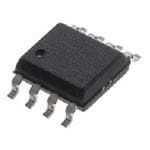
| 描述 | IC MOTOR CONTROLLER PAR 8SOIC马达/运动/点火控制器和驱动器 w/Rstrt & Flt Dtct |
| 产品分类 | PMIC - 电机, 电桥式驱动器集成电路 - IC |
| 品牌 | Microchip Technology |
| 产品手册 | |
| 产品图片 |
|
| rohs | 符合RoHS无铅 / 符合限制有害物质指令(RoHS)规范要求 |
| 产品系列 | 电源管理 IC,马达/运动/点火控制器和驱动器,Microchip Technology TC642BEOA- |
| 数据手册 | http://www.microchip.com/mymicrochip/filehandler.aspx?ddocname=en026002http://www.microchip.com/mymicrochip/filehandler.aspx?ddocname=en011685http://www.microchip.com/mymicrochip/filehandler.aspx?ddocname=en023833 |
| 产品型号 | TC642BEOA |
| 产品 | Fan / Motor Controllers / Drivers |
| 产品目录页面 | |
| 产品种类 | 马达/运动/点火控制器和驱动器 |
| 供应商器件封装 | 8-SOIC N |
| 关闭阈值 | 0.715 V |
| 功能 | 控制器 - 换向,方向管理 |
| 包装 | 管件 |
| 商标 | Microchip Technology |
| 安装类型 | 表面贴装 |
| 安装风格 | SMD/SMT |
| 封装 | Tube |
| 封装/外壳 | 8-SOIC(0.154",3.90mm 宽) |
| 封装/箱体 | SOIC-8 |
| 工作温度 | - 40 C to + 85 C |
| 工作电源电压 | 6 V |
| 工厂包装数量 | 100 |
| 应用 | 风扇控制器 |
| 接口 | 并联 |
| 标准包装 | 100 |
| 电压-电源 | 3 V ~ 5.5 V |
| 电压-负载 | - |
| 电机类型-AC,DC | 无刷 DC(BLDC) |
| 电机类型-步进 | - |
| 电流-输出 | - |
| 电源电流 | 400 uA |
| 类型 | Controller - PWM Fan |
| 输出配置 | 前级驱动器 |


- 商务部:美国ITC正式对集成电路等产品启动337调查
- 曝三星4nm工艺存在良率问题 高通将骁龙8 Gen1或转产台积电
- 太阳诱电将投资9.5亿元在常州建新厂生产MLCC 预计2023年完工
- 英特尔发布欧洲新工厂建设计划 深化IDM 2.0 战略
- 台积电先进制程称霸业界 有大客户加持明年业绩稳了
- 达到5530亿美元!SIA预计今年全球半导体销售额将创下新高
- 英特尔拟将自动驾驶子公司Mobileye上市 估值或超500亿美元
- 三星加码芯片和SET,合并消费电子和移动部门,撤换高东真等 CEO
- 三星电子宣布重大人事变动 还合并消费电子和移动部门
- 海关总署:前11个月进口集成电路产品价值2.52万亿元 增长14.8%


PDF Datasheet 数据手册内容提取
TC642B/TC647B PWM Fan Speed Controllers With Minimum Fan Speed, Fan Restart and FanSense™ Technology for Fault Detection Features Description • Temperature-Proportional Fan Speed for Acoustic The TC642B/TC647B devices are new versions of the Noise Reduction and Longer Fan Life existing TC642/TC647 fan speed controllers. These • Efficient PWM Fan Drive devices are switch mode, fan speed controllers that incorporate a new fan auto-restart function. Tempera- • 3.0V to 5.5V Supply Range: ture-proportional speed control is accomplished using - Fan Voltage Independent of TC642B/TC647B pulse width modulation. A thermistor (or other voltage Supply Voltage output temperature sensor) connected to the V input IN - Supports any Fan Voltage supplies the required control voltage of 1.20V to 2.60V • FanSense™ Fault Detection Circuit Protects (typical) for 0% to 100% PWM duty cycle. Minimum fan Against Fan Failure and Aids System Testing speed is set by a simple resistor divider on the V MIN • Shutdown Mode for "Green" Systems input. An integrated Start-Up Timer ensures reliable • Supports Low Cost NTC/PTC Thermistors motor start-up at turn-on, coming out of shutdown mode or following a transient fault. A logic-low applied • Over-Temperature Indication (TC642B only) to V (pin 3) causes fan shutdown. MIN • Fan Auto-Restart The TC642B and TC647B also feature Microchip • Space-Saving 8-Pin MSOP Package Technology's proprietary FanSense™ technology for Applications increasing system reliability. In normal fan operation, a pulse train is present at SENSE (pin 5). A missing- • Personal Computers & Servers pulse detector monitors this pin during fan operation. A • LCD Projectors stalled, open or unconnected fan causes the TC642B/ TC647B device to turn the V output on full (100% • Datacom & Telecom Equipment OUT duty cycle). If the fault persists (a fan current pulse is • Fan Trays not detected within a 32/f period), the FAULT output • File Servers goes low. Even with the FAULT output low, the V OUT • General Purpose Fan Speed Control output is on full during the fan fault condition in order to attempt to restart the fan. FAULT is also asserted if the Package Types PWM reaches 100% duty cycle (TC642B only), indicat- ing that maximum cooling capability has been reached MSOP, PDIP, SOIC and a possible overheating condition exists. The TC642B and TC647B devices are available in 8-pin V 1 8 V plastic MSOP, SOIC and PDIP packages. The specified IN DD temperature range of these devices is -40 to +85ºC. C 2 7 V F TC642B OUT V 3 TC647B 6 FAULT MIN GND 4 5 SENSE 2002-2013 Microchip Technology Inc. DS21756C-page 1
TC642B/TC647B Functional Block Diagram TC642B/TC647B V OTF V V IN DD Note Note: The V comparator OTF is for the TC642B device only. Control Logic CF 3xTPWM Timer V OUT Clock Generator Start-up Timer VMIN FAULT Missing V SHDN Pulse Detect SENSE 10k GND 70mV (typ) DS21756C-page 2 2002-2013 Microchip Technology Inc.
TC642B/TC647B 1.0 ELECTRICAL PIN FUNCTION TABLE CHARACTERISTICS Name Function Absolute Maximum Ratings † V Analog Input IN Supply Voltage (VDD).......................................................6.0V CF Analog Output Input Voltage, Any Pin................(GND - 0.3V) to (VDD +0.3V) VMIN Analog Input Operating Temperature Range....................- 40°C to +125°C GND Ground Maximum Junction Temperature, TJ...........................+150°C SENSE Analog Input ESD Protection on all pins........................................... > 3kV FAULT Digital (Open-Drain) Output † Notice: Stresses above those listed under “Maximum V Digital Output OUT Ratings” may cause permanent damage to the device. This is V Power Supply Input a stress rating only and functional operation of the device at DD those or any other conditions above those indicated in the operational listings of this specification is not implied. Expo- sure to maximum rating conditions for extended periods may affect device reliability. ELECTRICAL SPECIFICATIONS Electrical Specifications: Unless otherwise specified, all limits are specified for -40°C < T < +85°C, V = 3.0V to 5.5V. A DD Parameters Sym Min Typ Max Units Conditions Supply Voltage V 3.0 — 5.5 V DD Supply Current, Operating I — 200 400 µA Pins 6, 7 Open, DD C = 1µF, V = V F IN C(MAX) Supply Current, Shutdown Mode I — 30 — µA Pins 6, 7 Open, DD(SHDN) C = 1µF, V = 0.35V F MIN V Output OUT Sink Current at V Output I 1.0 — — mA V = 10% of V OUT OL OL DD Source Current at V Output I 5.0 — — mA V = 80% of V OUT OH OH DD V , V Inputs IN MIN Input Voltage at V or V for 100% V 2.45 2.60 2.75 V IN MIN C(MAX) PWM Duty Cycle Over-Temperature Indication V V + V For TC642B Only OTF C(MAX) Threshold 20mV Over-Temperature Indication V 80 mV For TC642B Only OTF-HYS Threshold Hysteresis V - V V 1.3 1.4 1.5 V C(MAX) C(MIN) C(SPAN) Minimum Speed Threshold V V - V V MIN C(MAX) C(MAX) V C(SPAN) Voltage Applied to V to Ensure V — — V x 0.13 V MIN SHDN DD Shutdown Mode Voltage Applied to V to Release V V x 0.19 — — V V = 5V MIN REL DD DD Shutdown Mode Hysteresis on V , V V — 0.03 x V — V SHDN REL HYST DD V , V Input Leakage I - 1.0 — +1.0 µA Note1 IN MIN IN Pulse-Width Modulator PWM Frequency f 26 30 34 Hz C = 1.0µF PWM F Note 1: Ensured by design, tested during characterization. 2: For V < 3.7V, t and t timers are typically 13/f. DD STARTUP MP 2002-2013 Microchip Technology Inc. DS21756C-page 3
TC642B/TC647B ELECTRICAL SPECIFICATIONS (CONTINUED) Electrical Specifications: Unless otherwise specified, all limits are specified for -40°C < T < +85°C, V = 3.0V to 5.5V. A DD Parameters Sym Min Typ Max Units Conditions SENSE Input SENSE Input Threshold Voltage with V 50 70 90 mV TH(SENSE) Respect to GND Blanking time to ignore pulse due to t — 3.0 — µsec BLANK V turn-on OUT FAULT Output Output Low Voltage V — — 0.3 V I = 2.5mA OL OL Missing Pulse Detector Timer t — 32/f — sec Note2 MP Start-Up Timer t — 32/f — sec Note2 STARTUP Diagnostic Timer t — 3/f — sec DIAG Note 1: Ensured by design, tested during characterization. 2: For V < 3.7V, t and t timers are typically 13/f. DD STARTUP MP TEMPERATURE SPECIFICATIONS Electrical Characteristics: Unless otherwise noted, all parameters apply at V = 3.0V to 5.5V DD Parameters Symbol Min Typ Max Units Conditions Temperature Ranges: Specified Temperature Range T -40 — +85 °C A Operating Temperature Range T -40 — +125 °C A Storage Temperature Range T -65 — +150 °C A Thermal Package Resistances: Thermal Package Resistance, 8-Pin MSOP — 200 — °C/W JA Thermal Package Resistance, 8-Pin SOIC — 155 — °C/W JA Thermal Package Resistance, 8-Pin PDIP — 125 — °C/W JA DS21756C-page 4 2002-2013 Microchip Technology Inc.
TC642B/TC647B TIMING SPECIFICATIONS t STARTUP V OUT FAULT SENSE FIGURE 1-1: TC642B/TC647B Start-Up Timing. 33.3msec (C = 1µF) F t DIAG t t MP MP V OUT FAULT SENSE FIGURE 1-2: Fan Fault Occurrence. t MP V OUT FAULT Minimum 16 pulses SENSE FIGURE 1-3: Recovery From Fan Fault. 2002-2013 Microchip Technology Inc. DS21756C-page 5
TC642B/TC647B C C 2 1 + 1µF 0.1µF VDD - 8 R V 1 1 VIN DD K3 R6 C 7 3 V + VIN 0.1µF OUT C8 - + Current 0.1µF limited - voltage source R2 3 TC642B VDD VMIN TC647B R C 5 4 K 4 + VMIN 0.1µF 6 - FAULT Current + limited - voltage 2 source CF 5 R4 GND SENSE K1 K2 4 R3 V SENSE C C C (pulse voltage source) 7 6 5 .01µF 1µF 0.1µF Note: C and C are adjusted to get the necessary 1µF value. 5 7 FIGURE 1-4: TC642B/TC647B Electrical Characteristics Test Circuit. DS21756C-page 6 2002-2013 Microchip Technology Inc.
TC642B/TC647B 2.0 TYPICAL PERFORMANCE CURVES Note: The graphs and tables provided following this note are a statistical summary based on a limited number of samples and are provided for informational purposes only. The performance characteristics listed herein are not tested or guaranteed. In some graphs or tables, the data presented may be outside the specified operating range (e.g., outside specified power supply range) and therefore outside the warranted range. Note: Unless otherwise indicated, V = 5V, T = +25°C. DD A 165 30.50 160 PCiFn =s 16 µ&F 7 Open VDD = 5.5V Hz) VDD = 3.0V CF = 1.0(cid:2)F 155 y ( 30.00 c n (µA)D 114550 VDD = 3.0V Freque 29.50 VDD = 5.5V ID 140 or at 135 cill 29.00 130 Os 125 28.50 -40 -25 -10 5 20 35 50 65 80 95 110 125 -40 -25 -10 5 20 35 50 65 80 95 110 125 Temperature (ºC) Temperature (ºC) FIGURE 2-1: I vs. Temperature. FIGURE 2-4: PWM Frequency vs. DD Temperature. 16 170 Pins 6 & 7 Open 1124 VDD = 5.0V 116605 CF =T 1A µ=F +90ºC TA = +125ºC I (mA)OL 1068 VDD = 5.5V VDD = 3.0V VDD = 4.0V I (µA)DD 111144550505 TA = -5ºC 4 135 2 130 TA = -40ºC 0 125 0 50 100 150 200 250 300 350 400 450 500 550 600 3 3.5 4 4.5 5 5.5 VOL (mV) VDD (V) FIGURE 2-2: PWM Sink Current (I ) vs. FIGURE 2-5: I vs. V . OL DD DD V . OL 16 30 14 12 VDD = 5.0V A) 27 VDD = 5.5V I (mA)OH 1068 VDD = 5.5V VDD = 3.0V VDD = 4.0V hutdown (µ 2214 VDD = 3.0V S 4 D 2 ID 18 Pins 6 & 7 Open VMIN = 0V 0 15 0 100 200 300 400 500 600 700 800 -40 -25 -10 5 20 35 50 65 80 95 110 125 VDD - VOH (mV) Temperature (ºC) FIGURE 2-3: PWM Source Current (I ) FIGURE 2-6: I Shutdown vs. OH DD vs. V -V . Temperature. DD OH 2002-2013 Microchip Technology Inc. DS21756C-page 7
TC642B/TC647B Note: Unless otherwise indicated, V = 5V, T = +25°C. DD A 70 74.0 IOL = 2.5 mA 73.5 60 VDD = 3.0V 73.0 VDD = 3.0V mV) 50 mV) 72.5 VDD = 4.0V V (OL 40 VDD = 4.0V (SE) 72.0 FAULT 30 VDD = 5.5V VDD = 5.0V VTH(SEN 777011...505 VDD = 5.5V VDD = 5.0V 20 70.0 10 69.5 -40 -25 -10 5 20 35 50 65 80 95 110 125 -40 -25 -10 5 20 35 50 65 80 95 110 125 Temperature (ºC) Temperature (ºC) FIGURE 2-7: FAULT V vs. FIGURE 2-10: Sense Threshold OL Temperature. (V ) vs. Temperature. TH(SENSE) 2.610 22 20 18 2.600 VDD = 5.5V A) 16 V (V)C(MAX) 2.590 VDD = 3.0V VDD = 5.0V AULT I (mOL 1110248 VDD = 5.5V VDD = 3.0V VDD = 4.0VVDD = 5.0V 2.580 F 6 4 CF = 1 µF 2 2.570 0 -40 -25 -10 5 20 35 50 65 80 95 110 125 0 50 100 150 200 250 300 350 400 Temperature (ºC) VOL (mV) FIGURE 2-8: V vs. Temperature. FIGURE 2-11: FAULT I vs. V . C(MAX) OL OL 1.220 45.00 CF = 1 µF VOH = 0.8VDD 40.00 VDD = 5.5V 1.210 35.00 A) VDD = 5.0V V) m 30.00 V (C(MIN) 1.200 VDD = 5.0V I (OUTOH 2205..0000 VDD = 4.0V V 1.190 VDD = 3.0V 15.00 10.00 VDD = 3.0V 1.180 5.00 -40 -25 -10 5 20 35 50 65 80 95 110 125 -40 -25 -10 5 20 35 50 65 80 95 110 125 Temperature (ºC) Temperature (ºC) FIGURE 2-9: V vs. Temperature. FIGURE 2-12: PWM Source Current (I ) C(MIN) OH vs. Temperature. DS21756C-page 8 2002-2013 Microchip Technology Inc.
TC642B/TC647B Note: Unless otherwise indicated, V = 5V, T = +25°C. DD A 30 2.630 VOL = 0.1VDD 25 VDD = 5.5V 2.625 VDD = 5.5V A) 20 VDD = 5.0V 2.620 VDD = 5.0V I (mUTOL 15 VDD = 4.0V V (V)OTF 22..661105 VDD = 3.0V VO 10 2.605 VDD = 3.0V 5 2.600 0 2.595 -40 -25 -10 5 20 35 50 65 80 95 110 125 -40 -25 -10 5 20 35 50 65 80 95 110 125 Temperature (ºC) Temperature (ºC) FIGURE 2-13: PWM Sink Current (I ) vs. FIGURE 2-16: V Threshold vs. OL OTF Temperature. Temperature. 0.80 100 00..7705 VDD = 5.5V V) 95 V (V)SHDN 0000....55660505 VDD = V5D.0D V= 4.0V ysteresis (m 8950 VDD = 5.5V VDD = 3.0V H 80 00..4405 VDD = 3.0V V OTF 75 0.35 0.30 70 -40 -25 -10 5 20 35 50 65 80 95 110 125 -40 -25 -10 5 20 35 50 65 80 95 110 125 Temperature (ºC) Temperature (ºC) FIGURE 2-14: V Threshold vs. FIGURE 2-17: Over-Temperature SHDN Temperature. Hysteresis (V ) vs. Temperature. OTF-HYS 1.00 0.95 VDD = 5.5V 0.90 0.85 0.80 VDD = 5.0V V) 0.75 (EL 0.70 VR 0.65 VDD = 4.0V 0.60 0.55 0.50 0.45 VDD = 3.0V 0.40 -40 -25 -10 5 20 35 50 65 80 95 110 125 Temperature (ºC) FIGURE 2-15: V Threshold vs. REL Temperature. 2002-2013 Microchip Technology Inc. DS21756C-page 9
TC642B/TC647B 3.0 PIN FUNCTIONS 3.5 Digital (Open-Drain) Output (FAULT) The description of the pins are given in Table3-1. The FAULT line goes low to indicate a fault condition. TABLE 3-1: PIN FUNCTION TABLE When FAULT goes low due to a fan fault, the output will remain low until the fan fault condition has been Pin Name Function removed (16 pulses have been detected at the SENSE 1 VIN Analog Input pin in a 32/f period). For the TC642B device, the FAULT 2 CF Analog Output output will also be asserted when the VIN voltage reaches the V treshold of 2.62V (typical). This gives 3 V Analog Input OTF MIN an over-temperature/100% fan speed indication. 4 GND Ground 5 SENSE Analog Input 3.6 Digital Output (VOUT) 6 FAULT Digital (Open-Drain) Output V is an active-high complimentary output and OUT 7 V Digital Output drives the base of an external NPN transistor (via an OUT 8 V Power Supply Input appropriate base resistor) or the gate of an N-channel DD MOSFET. This output has asymmetrical drive. During a fan fault condition, the V output is continuously on. OUT 3.1 Analog Input (V ) IN 3.7 Power Supply Input (V ) The thermistor network (or other temperature sensor) DD connects to VIN. A voltage range of 1.20V to 2.60V (typ- The VDD pin with respect to GND provides power to the ical) on this pin drives an active duty cycle of 0% to device. This bias supply voltage may be independent of 100% on the VOUT pin. the fan power supply. 3.2 Analog Output (C ) F C is the positive terminal for the PWM ramp generator F timing capacitor. The recommended value for the C F capacitor is 1.0µF for 30Hz PWM operation. 3.3 Analog Input (V ) MIN An external resistor divider connected to V sets the MIN minimum fan speed by fixing the minimum PWM duty cycle (1.20V to 2.60V = 0% to 100%, typical). The TC642B and TC647B devices enter shutdown mode when 0 V V . During shutdown, the FAULT MIN SHDN output is inactive and supply current falls to 30µA (typical). 3.4 Analog Input (SENSE) Pulses are detected at SENSE as fan rotation chops the current through a sense resistor. The absence of pulses indicates a fan fault condition. DS21756C-page 10 2002-2013 Microchip Technology Inc.
TC642B/TC647B 4.0 DEVICE OPERATION special heatsinking to remove the power being dissipated in the package. The TC642B/TC647B devices are a family of tempera- The other advantage of the PWM approach is that the ture proportional, PWM mode, fan speed controllers. voltage being applied to the fan is always near 12V. Features of the family include minimum fan speed, fan This eliminates any concern about not supplying a high auto-shutdown mode, fan auto-restart, remote shut- enough voltage to run the internal fan components, down, over-temperature indication and fan fault which is very relevant in linear fan speed control. detection. The TC642B/TC647B family is slightly different from 4.2 PWM Fan Speed Control the original TC64X family, which includes the TC642, TC646, TC647, TC648 and TC649 devices. Changes The TC642B and TC647B devices implement PWM fan speed control by varying the duty cycle of a fixed fre- have been made to adjust the operation of the device quency pulse train. The duty cycle of a waveform is the during a fan fault condition. on time divided by the total period of the pulse. For The key change to the TC64XB family of devices example, a 100Hz waveform (10ms) with an on time (TC642B, TC647B, TC646B, TC648B, TC649B) is that of 5.0ms has a duty cycle of 50% (5.0ms / 10.0ms). the FAULT and V outputs no longer “latch” to a state OUT This example is illustrated in Figure4-1. during a fan fault condition. The TC64XB family will continue to monitor the operation of the fan so that when the fan returns to normal operation, the fan speed t controller will also return to normal operation (PWM mode). The operation and features of these devices are discussed in the following sections. 4.1 Fan Speed Control Methods The speed of a DC brushless fan is proportional to the ton toff voltage across it. This relationship will vary from fan to fan and should be characterized on an individual basis. D = Duty Cycle t = Period The speed versus applied voltage relationship can then D = t / t t = 1/f on be used to set up the fan speed control algorithm. f = Frequency There are two main methods for fan speed control. The first is pulse width modulation (PWM) and the second FIGURE 4-1: Duty Cycle of a PWM is linear. Using either method, the total system power Waveform. requirement to run the fan is equal. The difference The TC642B and TC647B generate a pulse train with a between the two methods is where the power is typical frequency of 30Hz (C = 1µF). The duty cycle consumed. F can be varied from 0% to 100%. The pulse train gener- The following example compares the two methods for ated by the TC642B/TC647B device drives the gate of a 12V, 120mA fan running at 50% speed. With 6V an external N-channel MOSFET or the base of an NPN applied across the fan, the fan draws an average transistor (shown in Figure4-2). See Section5.5, “Out- current of 68mA. put Drive Device Selection”, for more information. Using a linear control method, there is 6V across the fan and 6V across the drive element. With 6V and 68mA, the drive element is dissipating 410mW of 12V power. Using the PWM approach, the fan voltage is modulated at a 50% duty cycle with most of the 12V being dropped FAN across the fan. With 50% duty cycle, the fan draws an V DD RMS current of 110mA and an average current of 72mA. Using a MOSFET with a 1R (a fairly DS(on) D typical value for this low current), the power dissipation Q in the drive element would be: 12mW (Irms2 * RDS(on)). TC642B VOUT G DRIVE Using a standard 2N2222A NPN transistor (assuming TC647B S a Vce-sat of 0.8V), the power dissipation would be 58mW (Iavg* Vce-sat). GND The PWM approach to fan speed control results in much less power dissipation in the drive element, allowing smaller devices to be used while not requiring FIGURE 4-2: PWM Fan Drive. 2002-2013 Microchip Technology Inc. DS21756C-page 11
TC642B/TC647B By modulating the voltage applied to the gate of the 4.4 PWM Frequency & Duty Cycle Control MOSFET (QDRIVE), the voltage that is applied to the (CF & VIN Pins) fan is also modulated. When the V pulse is high, the OUT gate of the MOSFET is turned on, pulling the voltage at The frequency of the PWM pulse train is controlled by the drain of QDRIVE to zero volts. This places the full the CF pin. By attaching a capacitor to the CF pin, the 12V across the fan for the t period of the pulse. When frequency of the PWM pulse train can be set to the on the duty cycle of the drive pulse is 100% (full on, desired value. The typical PWM frequency for a 1.0F t =t), the fan will run at full speed. As the duty cycle capacitor is 30Hz. The frequency can be adjusted by on is decreased (pulse on time “ton” is lowered), the fan raising or lowering the value of the capacitor. The CF will slow down proportionally. With the TC642B and pin functions as a ramp generator. The voltage at this TC647B devices, the duty cycle is controlled by either pin will ramp from 1.20V to 2.60V (typically) as a saw- the V or V input, with the higher voltage setting the tooth waveform. An example of this is shown in IN MIN duty cycle. This is described in more detail in Section Figure4-3. 5.5, “Output Drive Device Selection”. 2.8 4.3 Fan Start-up CF = 1 µF VCMAX 2.6 Often overlooked in fan speed control is the actual start- 2.4 up control period. When starting a fan from a non-oper- V) 2.2 ating condition (fan speed is zero revolutions per minute ge ( 2.0 a (RPM)), the desired PWM duty cycle or average fan olt 1.8 V voltage can not be applied immediately. Since the fan is C F 1.6 at a rest position, the fan’s inertia must be overcome to 1.4 get it started. The best way to accomplish this is to apply 1.2 VCMIN the full rated voltage to the fan for a minimum of one 1.0 0 20 40 60 80 100 second. This will ensure that in all operating environ- ments, the fan will start and operate properly. An exam- Time (msec) ple of the start-up timing is shown in Figure 1-1. FIGURE 4-3: C Pin Voltage. F A key feature of the TC642B/TC647B device is the The duty cycle of the PWM output is controlled by the start-up timer. When power is first applied to the device, voltage at the V input pin (or the V voltage, which- (when the device is brought out of the shutdown mode IN MIN ever is greater). The duty cycle of the PWM output is of operation) the V output will go to a high state for OUT produced by comparing the voltage at the V pin to the 32PWM cycles (one second for C = 1F). This will IN F voltage ramp at the C pin. When the voltage at the V drive the fan to full speed for this time-frame. F IN pin is 1.20V, the duty cycle will be 0%. When the volt- During the start-up period, the SENSE pin is being age at the V pin is 2.60V, the PWM duty cycle will be IN monitored for fan pulses. If pulses are detected during 100% (these are both typical values). The V to PWM IN this period, the fan speed controller will then move to duty cycle relationship is shown in Figure4-4. PWM operation (see Section4.5, “Minimum Fan The lower value of 1.20V is referred to as V and Speed”, for more details on operation when coming out CMIN the 2.60V threshold is referred to as V . A calcula- of start-up). If pulses are not detected during the start- CMAX tion for duty cycle is shown in the equation below. The up period, the start-up timer is activated again. If pulses voltage range between V and V is character- are not detected at the SENSE pin during this addi- CMIN CMAX ized as V and has a typical value of 1.4V with tional start-up period, the FAULT output will go low to CSPAN minimum and maximum values of 1.3V and 1.5V, indicate that a fan fault condition has occurred. See respectively. Section4.7, “FAULT Output”, for more details. EQUATION PWM DUTY CYCLE (V - V ) * 100 IN CMIN Duty Cycle (%) = V - V CMAX CMIN DS21756C-page 12 2002-2013 Microchip Technology Inc.
TC642B/TC647B If the voltage at the V pin falls below 1.76V, the duty IN 100 cycle of the VOUT output will not decrease below the 90 40% value that is now set by the voltage at the VMIN 80 pin. In this manner, the fan will continue to operate at %) 70 40% speed even when the temperature (voltage at V ) e (60 continues to decrease. IN cl y50 C For the TC642B and TC647B devices, the V pin is y 40 MIN Dut30 also used as the shutdown pin. The VSHDN and VREL 20 threshold voltages are characterized in the “Electrical 10 Characteristics” table of Section1.0. If the VMIN pin 0 voltage is pulled below the V threshold, the device SHDN 1 1.2 1.4 1.6 1.8 2 2.2 2.4 2.6 2.8 will shut down (V output goes to a low state, the OUT V (V) IN FAULT pin is inactive). If the voltage on the V pin MIN then rises above the release threshold (V ), the FIGURE 4-4: V voltage vs. PWM duty REL IN device will go through a Power-Up sequence. The cycle(Typical). Power-Up sequence is shown later in Figure4-9. The PWM duty cycle is also controlled by the V pin MIN 4.6 V Output (PWM Output) See Section4.5, “Minimum Speed (VMIN Pin)”, for OUT more details on this function. The V output is a digital output designed for driving OUT the base of a transistor or the gate of a MOSFET. The 4.5 Minimum Speed (V Pin) MIN V output is designed to be able to quickly raise the OUT base current or the gate voltage of the external drive For the TC642B and TC647B devices, pin 3 is the V MIN pin. This pin is used for setting the minimum fan speed device to its final value. threshold. When the device is in shutdown mode, the V output OUT The minimum fan speed function provides a way to set is actively held low. The output can be varied from 0% a threshold for a minimum duty cycle on the V out- duty cycle (full off) to 100% duty cycle (full on). As pre- OUT put. This in turn produces a minimum fan speed for the viously discussed, the duty cycle of the VOUT output is user. The voltage range for the VMIN pin is the same as controlled via the VIN input voltage along with the VMIN that for the V pin (1.20V to 2.60V). The voltage at the voltage. IN VMIN pin is set in this range so that as the voltage at the A base current-limiting resistor is required when using VIN pin decreases below the VMIN voltage, the output a transistor as the external drive device in order to limit duty cycle will be controlled by the VMIN voltage. The the amount of drive current that is drawn from the VOUT following equation can be used to determine the neces- output. sary voltage at V for a desired minimum duty cycle MIN The V output can be directly connected to the gate on V . OUT OUT of an external MOSFET. One concern when doing this, though, is that the fast turn-off time of the fan drive EQUATION V VOLTAGE MIN MOSFET can cause a problem. The fan motor looks like an inductor. When the MOSFET is turned off VMIN (V) = (DC * 1.4) + 1.20 quickly, the current in the fan wants to continue to flow 100 in the same direction. This causes the voltage at the drain of the MOSFET to rise. If there aren’t any clamp DC = Desired Duty Cycle diodes internal to the fan, this voltage can rise above the drain-to-source voltage rating of the MOSFET. For Example: If a minimum duty cycle of 40% is desired, this reason, an external clamp diode is suggested. This the V voltage should be set to: MIN is shown in Figure4-5. EXAMPLE 4-1: V (V) = (40 * 1.4) + 1.20 MIN 100 V = 1.76V MIN 2002-2013 Microchip Technology Inc. DS21756C-page 13
TC642B/TC647B During a fan fault condition, the FAULT output will remain low until the fault condition has been removed. During this time, the V output is driven high contin- OUT uously to attempt to restart the fan, and the SENSE pin Clamp Diode is monitored for fan pulses. If a minimum of 16 pulses FAN are detected at the SENSE input over a 32cycle time period (one second for C = 1.0F), the fan fault con- F dition no longer exists. The FAULT output is then released and the V output returns to normal PWM OUT operation, as dictated by the V and V inputs. IN MIN Q V 1 OUT If the V voltage is pulled below the V level dur- MIN SHDN ing a fan fault condition, the FAULT output will be released and the V output will be shutdown OUT RSENSE (VOUT=0V). If the VMIN voltage then increases above the V threshold, the device will go through the REL normal start-up routine. If, during a fan fault condition, the voltage at the V pin IN GND drops below the VMIN voltage level, the TC642B/ TC647B device will continue to hold the FAULT line low Q1: N-Channel MOSFET and drive the VOUT output to 100% duty cycle. If the fan fault condition is then removed, the FAULT output will FIGURE 4-5: Clamp Diode for Fan. be released and the V output will be driven to the OUT duty cycle that is being commanded by the V input. MIN 4.7 FAULT Output The sink current capability of the FAULT output is listed The FAULT output is an open-drain, active-low output. in the “Electrical Characteristics” table of Section 1.0. For the TC642B and TC647B devices, the FAULT out- 4.8 Sensing Fan Operation (SENSE) put indicates when a fan fault condition has occurred. For the TC642B device, the FAULT output also indi- The SENSE input is an analog input used to monitor cates when an over-temperature (OTF) condition has the fan’s operation. It does this by sensing fan current occurred. pulses, which represent fan rotation. When a fan rotates, commutation of the fan current occurs as the For the TC642B device, an over-temperature condition fan poles pass the armatures of the motor. The commu- is indicated (FAULT output is pulled low) when the V IN tation of the fan current makes the current waveshape input reaches the V threshold voltage (the V OTF OTF appear as pulses. There are two typical current wave- threshold voltage is typically 20mV higher than the forms of brushless DC fan motors. These are shown in V threshold and has 80mV of hysteresis). This CMAX Figures4-6 and4-7. indicates that maximum cooling capacity has been reached (the fan is at full speed) and that an overheat- ing situation can occur. When the voltage at the V IN input falls below the V threshold voltage by the hys- OTF teresis value (V ), the FAULT output returns to OTF-HYS the high-state (a pull-up resistor is needed on the FAULT output). A fan fault condition is indicated when fan current pulses are no longer detected at the SENSE pin. Pulses at the SENSE pin indicate that the fan is spinning and conducting current. If pulses are not detected at the SENSE pin for 32PWM cycles, the 3-cycle diagnostic timer is fired. This means that the V output is high for 3PWM cycles. If pulses OUT are detected in this 3-cycle period, then normal PWM operation is resumed and no fan fault is indicated. If no pulses are detected in the 3-cycle period, the start-up timer is activated and the V output is driven high for OUT 32PWM cycles. If pulses are detected during this time- frame, normal PWM operation is resumed. If no pulses FIGURE 4-6: Fan Current With DC Offset are detected during this time frame, a fan fault condition exists and the FAULT output is pulled low. And Positive Commutation Current. DS21756C-page 14 2002-2013 Microchip Technology Inc.
TC642B/TC647B . across RSENSE and presents only the voltage pulse portion to the SENSE pin of the TC642B/TC647B devices. The R and C values need to be selected so SENSE SENSE that the voltage pulse provided to the SENSE pin is 70mV (typical) in amplitude. Be sure to check the sense pulse amplitude over all operating conditions (duty cycles), as the current pulse amplitude will vary with duty cycle. See Section5.0, “Applications Informa- tion”, for more details on selecting values for R SENSE and C . SENSE Key features of the SENSE pin circuitry are an initial blanking period after every V pulse and an initial OUT pulse blanker. The TC642B/TC647B sense circuitry has a blanking period that occurs at the turn-on of each V pulse. OUT During this blanking period, the sense circuitry ignores any pulse information that is seen at the SENSE pin input. This stops the TC642B/TC647B device from FIGURE 4-7: Fan Current With falsely sensing a current pulse which is due to the fan Commutation Pulses To Zero. drive device turn-on. The SENSE pin senses positive voltage pulses that The initial pulse blanker is also implemented to stop have an amplitude of 70mV (typical value). When a false sensing of fan current pulses. When a fan is in a pulse is detected, the missing pulse detector timer is locked rotor condition, the fan current no longer com- reset. As previously stated, if the missing pulse detec- mutates, it simply flows through one fan winding and is tor timer reaches the time for 32cycles, the loop for a DC current. When a fan is in a locked rotor condition diagnosing a fan fault is engaged (diagnostic timer, and the TC642B/TC647B device is in PWM mode, it then the start-up timer). will see one current pulse each time the V output is OUT Both of the fan current waveshapes that are shown in turned on. The initial pulse blanker allows the TC642B/ Figures4-6 and4-7 can be sensed with the sensing TC647B device to ignore this pulse and recognize that scheme shown in Figure4-8. the fan is in a fault condition. 4.9 Behavioral Algorithms The behavioral algorithm for the TC642B/TC647B devices is shown in Figure4-9. FAN The behavioral algorithm shows the step-by-step deci- sion-making process for the fan speed controller oper- TC64XB ation. The TC642B and TC647B devices are very R ISO similar with one exception: the TC647B device does V OUT not implement the over-temperature portion of the algorithm. SENSE C SENSE GND (0.1µF typical) RSENSE FIGURE 4-8: Sensing Scheme For Fan Current. The fan current flowing through R generates a SENSE voltage that is proportional to the current. The C SENSE capacitor removes any DC portion of the voltage 2002-2013 Microchip Technology Inc. DS21756C-page 15
TC642B/TC647B Normal Power-Up Operation Power-on Clear Missing Reset Pulse Detector FAULT = 1 Yes Shutdown VMIN < VSHDN? VOUT = 0 Yes Shutdown No VMIN < VSHDN? VOUT = 0 No VMIN > VREL? No Yes No VMIN > VREL ? Fire Start-up Yes Timer (1 sec) Yes Power-Up VIN > VOTF? Fire Start-up Fan Pulse No Timer FAULT = 0 Detected? (1 sec) Yes No Yes Fan Pulse TC642B Only Detected? VOUT Proportional to Greater ONpoerrmataiol n No of VIN or VMIN Fan Fault Yes Fan Pulse No Detected? M.P.D. No Expired? Yes Fire Diagnostic Timer (100 msec) Yes Fan Pulse No Fire Start-up Fan Fault Timer Detected? (1 sec) FAULT = Low, Yes VOUT = High Fan Pulse Detected? No VMIN<VSHD N? Yes SVhOuUtdT o=w 0n Fan Fault No No Yes No 16 Pulses VMIN > VREL ? Powe r-Up Detected? Yes Normal Operation FIGURE 4-9: TC642B/TC647B Behavioral Algorithm. DS21756C-page 16 2002-2013 Microchip Technology Inc.
TC642B/TC647B 5.0 APPLICATIONS INFORMATION V DD 5.1 Setting the PWM Frequency I DIV The PWM frequency of the V output is set by the OUT capacitor value attached to the C pin. The PWM fre- F quency will be 30Hz (typical) for a 1µF capacitor. The relationship between frequency and capacitor value is RT R1 linear, making alternate frequency selections easy. V As stated in previous sections, the PWM frequency IN should be kept in the range of 15Hz to 35Hz. This will eliminate the possibility of having audible frequencies R 2 when varying the duty cycle of the fan drive. A very important factor to consider when selecting the PWM frequency for the TC642B/TC647B devices is the FIGURE 5-1: Temperature Sensing RPM rating of the selected fan and the minimum duty Circuit. cycle that the fan will be operating at. For fans that have a full speed rating of 3000RPM or less, it is desirable Figure5-1 represents a temperature-dependent volt- to use a lower PWM frequency. A lower PWM fre- age divider circuit. R is a conventional NTC thermistor, T quency allows for a longer time period to monitor the while R and R are standard resistors. R and R form 1 2 1 T fan current pulses. The goal is to be able to monitor at a parallel resistor combination that will be referred to as least two fan current pulses during the on time of the R (R = R * R / R + R ). As the temperature TEMP TEMP 1 T 1 T VOUT output. increases, the value of Rt decreases and the value of Example: The system design requirement is to operate RTEMP will decrease with it. Accordingly, the voltage at the fan at 50% duty cycle when ambient temperatures VIN increases as temperature increases, giving the are below 20°C. The fan full speed RPM rating is desired relationship for the VIN input. R1 helps to linear- 3000RPM and has four current pulses per rotation. At ize the response of the sense network and aids in 50% duty cycle, the fan will be operating at obtaining the proper VIN voltages over the desired tem- approximately 1500RPM. perature range. An example of this is shown in Figure5-2. EQUATION If less current draw from V is desired, a larger value DD thermistor should be chosen. The voltage at the V pin 601000 IN Time for one revolution (msec.) = ------------------------ = 40 can also be generated by a voltage output temperature 1500 sensor device. The key is to get the desired V voltage IN to system (or component) temperature relationship. If one fan revolution occurs in 40msec, each fan pulse The following equations apply to the circuit in occurs 10msec apart. In order to detect two fan current Figure5-1. pulses, the on time of the V pulse must be at least OUT 20msec. With the duty cycle at 50%, the total period of EQUATION one cycle must be at least 40msec, which makes the PWM frequency 25Hz. For this example, a PWM fre- V R quency of 20Hz is recommended. This would define a VT1 = --------------D----D-------------2----------- R T1+R C capacitor value of 1.5µF. TEMP 2 F V R 5.2 Temperature Sensor Design DD 2 VT2 = ------------------------------------------ R T2+R TEMP 2 As discussed in previous sections, the V analog input IN has a range of 1.20V to 2.60V (typical), which repre- In order to solve for the values of R and R , the values sents a duty cycle range on the V output of 0% to 1 2 OUT for V , and the temperatures at which they are to 100%, respectively. The V voltages can be thought of IN IN occur, need to be selected. The variables T1 and T2 as representing temperatures. The 1.20V level is the represent the selected temperatures. The value of the low temperature at which the system requires very little thermistor at these two temperatures can be found in cooling. The 2.60V level is the high temperature, for the thermistor data sheet. With the values for the which the system needs maximum cooling capability thermistor and the values for V , there are now two (100% fan speed). IN equations from which the values for R and R can be 1 2 One of the simplest ways of sensing temperature over found. a given range is to use a thermistor. By using an NTC thermistor, as shown in Figure5-1, a temperature variant voltage can be created. 2002-2013 Microchip Technology Inc. DS21756C-page 17
TC642B/TC647B Example: The following design goals are desired: 5.4 FanSense Network • Duty Cycle = 50% (VIN = 1.90V) with (RSENSE and CSENSE) Temperature (T1) = 30°C The FanSense Network (comprised of R and SENSE • Duty Cycle = 100% (V = 2.60V) with IN C ) allows the TC642B and TC647B devices to SENSE Temperature (T2) = 60°C detect commutation of the fan motor. R converts SENSE Using a 100k thermistor (25°C value), look up the the fan current into a voltage. C AC couples this SENSE thermistor values at the desired temperatures: voltage signal to the SENSE pin. The goal of the sense network is to provide a voltage pulse to the SENSE pin • R (T1) = 79428 @ 30°C T that has a minimum amplitude of 90mV. This will • R (T2) = 22593 @ 60°C T ensure that the current pulse caused by the fan Substituting these numbers into the given equations commutation is recognized by the TC642B/TC647B produces the following numbers for R1 and R2. device. • R1 = 34.8k A 0.1µF ceramic capacitor is recommended for • R2 = 14.7k CSENSE. Smaller values will require that larger sense resistors be used. Using a 0.1µF capacitor results in reasonable values for R . Figure5-3 illustrates a SENSE 140 4.000 typical SENSE network. (cid:3)) 120 VIN Voltage 3.500 e (k 100 3.000 c Resistan 6800 22..050000 V (V)IN FAN k NTC Thermistor 1.500 Networ 40 100 k(cid:3) @ 25ºC 1.000 VOUT RISO 20 RTEMP 0.500 715 0 0.000 20 30 40 50 60 70 80 90 100 Temperature (ºC) SENSE C SENSE R SENSE FIGURE 5-2: How Thermistor Resistance, (0.1µF typical) V , and R Vary With Temperature. IN TEMP Note: See Table5-1 for R values. Figure5-2 graphs R , R (R in parallel with R ) SENSE T TEMP 1 T and V versus temperature for the example shown IN FIGURE 5-3: Typical Sense Network. above. The required value of R will change with the cur- SENSE 5.3 Thermistor Selection rent rating of the fan and the fan current waveshape. A key point is that the current rating of the fan specified As with any component, there are a number of sources by the manufacturer may be a worst-case rating, with for thermistors. A listing of companies that manufacture the actual current drawn by the fan being lower. For the thermistors can be found at www.temperatures.com/ purposes of setting the value for R , the operating thermivendors.html. This website lists over forty SENSE fan current should be measured to get the nominal suppliers of thermistor products. A brief list is shown value. This can be done by using an oscilloscope cur- here. rent probe or by using a voltage probe with a low value - Thermometrics® - Quality Thermistor™ resistor (0.5). Another good tool for this exercise is - Ametherm® - Sensor Scientific™ the TC642 Evaluation Board. This board allows the R and C values to be easily changed while - U.S. Sensors™ - Vishay® SENSE SENSE allowing the voltage waveforms to be monitored to - Advanced Thermal - muRata® ensure the proper levels are being reached. Products™ Table5-1 shows values of R according to the SENSE nominal operating current of the fan. The fan currents are average values. If the fan current falls between two of the values listed, use the higher resistor value. DS21756C-page 18 2002-2013 Microchip Technology Inc.
TC642B/TC647B TABLE 5-1: FAN CURRENT VS. R Another important factor to consider when selecting the SENSE R value is the fan current value during a locked Nominal Fan Current SENSE R () rotor condition. When a fan is in a locked rotor condition (mA) SENSE (fan blades are stopped even though power is being 50 9.1 applied to the fan), the fan current can increase dra- 100 4.7 matically, often 2.5 to 3.0 times the normal operating fan current. This will effect the power rating of the 150 3.0 R resistor selected. SENSE 200 2.4 When selecting the fan for the application, the current 250 2.0 draw of the fan during a locked rotor condition should 300 1.8 be considered, especially if multiple fans are being 350 1.5 used in the application. 400 1.3 There are two main types of fan designs when looking at fan current draw during a locked rotor condition. 450 1.2 The first is a fan that will simply draw high DC currents 500 1.0 when put into a locked rotor condition. Many older fans The values listed in Table5-1 are for fans that have the were designed this way. An example of this is a fan that fan current waveshape shown in Figure4-7. With this draws an average current of 100mA during normal waveshape, the average fan current is closer to the operation. In a locked rotor condition, this fan will draw peak value, which requires the resistor value to be 250mA of average current. For this design, the higher. When using a fan that has the fan current wave- R power rating must be sized to handle the SENSE shape shown in Figure4-6, the resistor value can often 250mA condition. The fan bias supply must also take be decreased since the current peaks are higher than this into account. the average and it is the AC portion of the voltage that The second style design, which represents many of the gets coupled to the SENSE pin. newer fan designs today, acts to limit the current in a The key point when selecting an RSENSE value is to try locked rotor condition by going into a pulse mode of to minimize the value in order to minimize the power operation. An example of the fan current waveshape dissipation in the resistor. In order to do this, it is critical for this style fan is shown in Figure5-5. The fan repre- to know the waveshape of the fan current and not just sented in Figure5-5 is a Panasonic®, 12V, 220mA fan. the average value. During the on time of the waveform, the fan current is Figure5-4 shows some typical waveforms for the fan peaking up to 550mA. Due to the pulse mode opera- current and the voltage at the SENSE pin. tion, however, the actual RMS current of the fan is very near the 220mA rating. Because of this, the power rat- ing for the R resistor does not have to be over- SENSE sized for this application. FIGURE 5-4: Typical Fan Current and SENSE Pin Waveforms. 2002-2013 Microchip Technology Inc. DS21756C-page 19
TC642B/TC647B FIGURE 5-5: Fan Current During a Locked Rotor Condition. 5.5 Output Drive Device Selection The following is recommended: • Ask how the fan is designed. If the fan has clamp The TC642B/TC647B is designed to drive an external diodes internally, this problem will not be seen. If NPN transistor or N-channel MOSFET as the fan the fan does not have internal clamp diodes, it is a speed modulating element. These two arrangements good idea to put one externally (Figure5-6). Put- are shown in Figure5-7. For lower current fans, NPN ting a resistor between V and the gate of the transistors are a very economical choice for the fan OUT MOSFET will also help slow down the turn-off and drive device. It is recommended that, for higher current limit this condition. fans (300mA and above), MOSFETs be used as the fan drive device. Table5-2 provides some possible part numbers for use as the fan drive element. When using a NPN transistor as the fan drive element, a base current-limiting resistor must be used, as is shown in Figure5-7. FAN When using MOSFETs as the fan drive element, it is very easy to turn the MOSFETs on and off at very high rates. Because the gate capacitances of these small MOSFETs are very low, the TC642B/TC647B can charge and discharge them very quickly, leading to V Q1 OUT very fast edges. Of key concern is the turn-off edge of the MOSFET. Since the fan motor winding is essentially an inductor, once the MOSFET is turned off, the current that was flowing through the motor wants to continue to RSENSE flow. If the fan does not have internal clamp diodes around the windings of the motor, there is no path for this current to flow through, and the voltage at the drain of the MOSFET may rise until the drain-to-source rating GND of the MOSFET is exceeded. This will most likely cause Q : N-Channel MOSFET the MOSFET to go into avalanche mode. Since there is 1 very little energy in this occurrence, it will probably not fail the device, but it would be a long-term reliability FIGURE 5-6: Clamp Diode For Fan Turn- issue. Off. DS21756C-page 20 2002-2013 Microchip Technology Inc.
TC642B/TC647B Fan Bias Fan Bias FAN FAN R BASE VOUT Q1 V Q1 OUT R R SENSE SENSE GND GND a) Single Bipolar Transistor b) N-Channel MOSFET FIGURE 5-7: Output Drive Device Configurations. TABLE 5-2: FAN DRIVE DEVICE SELECTION TABLE (NOTE2) Max Vbe sat / V /V Fan Current Suggested Device Package Min hfe CE DS Vgs(V) (V) (mA) Rbase () MMBT2222A SOT-23 1.2 50 40 150 800 MPS2222A TO-92 1.2 50 40 150 800 MPS6602 TO-92 1.2 50 40 500 301 SI2302 SOT-23 2.5 NA 20 500 Note1 MGSF1N02E SOT-23 2.5 NA 20 500 Note1 SI4410 SO-8 4.5 NA 30 1000 Note1 SI2308 SOT-23 4.5 NA 60 500 Note1 Note 1: A series gate resistor may be used in order to control the MOSFET turn-on and turn-off times. 2: These drive devices are suggestions only. Fan currents listed are for individual fans. 5.6 Bias Supply Bypassing and Noise 5.7 Design Example/Typical Filtering Application The bias supply (V ) for the TC642B/TC647B devices The system has been designed with the following DD should be bypassed with a 1.0F ceramic capacitor. components and criteria. This capacitor will help supply the peak currents that System inlet air ambient temperature ranges from 0ºC are required to drive the base/gate of the external fan to 50ºC. At 20ºC and below, it is desired to have the drive devices. system cooling stay at a constant level. At 20ºC, the fan As the V pin controls the duty cycle in a linear fashion, should be run at 40% of its full fan speed. Full fan IN any noise on this pin can cause duty-cycle jittering. For speed should be reached when the ambient air is 40ºC. this reason, the V pin should be bypassed with a IN The system has a surface mount, NTC-style thermistor 0.01µF capacitor. in a 1206 package. The thermistor is mounted on a In order to keep fan noise off of the TC642B/TC647B daughtercard, which is directly in the inlet air stream. device ground, individual ground returns for the The thermistor is a NTC, 100k @ 25ºC, Thermomet- TC642B/TC647B and the low side of the fan current rics® part number NHQ104B425R5. The given Beta for sense resistor should be used. the thermistor is 4250. The system bias voltage to run the fan controller is 5V and the fan voltage is 12V. 2002-2013 Microchip Technology Inc. DS21756C-page 21
TC642B/TC647B The fan used in the system is a Panasonic®, Panaflo®- series fan, model number FBA06T12H. A fault indication is desired when the fan is in a locked rotor condition. This signal is used to indicate to the system that cooling is not available and a warning should be issued to the user. No fault indication from the fan controller is necessary for an over-temperature condition, as this is being reported elsewhere. Step 1: Gathering Information. The first step in the design process is to gather the needed data on the fan and thermistor. For the fan, it is also a good idea to look at the fan current waveform, as indicated earlier in the data sheet. Fan Information: Panasonic number: FBA06T12H - Voltage = 12V - Current = 145mA (number from data sheet ) FIGURE 5-9: FBA06T12H Locked rotor fan current. From Figure5-9 it is seen that in a locked-rotor fault condition, the fan goes into a pulsed current mode of operation. During this mode, when the fan is conduct- ing current, the peak current value is 360mA for peri- ods of 200msec. This is significantly higher than the average full fan speed current shown in Figure5-8. However, because of the pulse mode, the average fan current in a locked-rotor condition is lower and was measured at 68mA. The RMS current during this mode, which is necessary for current sense resistor (R ) value selection, was measured at 154mA. SENSE This is slightly higher than the RMS value during full fan speed operation. Thermistor Information: Thermometrics part number: FIGURE 5-8: FBA06T12H fan current NHQ104B425R5 waveform. Resistance Value: 100k @ 25ºC From the waveform in Figure5-8, the fan current has Beta Value (): 4250 an average value of 120mA, with peaks up to 150mA. From this information, the thermistor values at 20ºC This information will help in the selection of the R SENSE and 40ºC must be found. This information is needed in and C values later on. Also of interest for the SENSE order to select the proper resistor values for R and R R selection value is what the fan current does in 1 2 SENSE (see Figure5-13), which sets the V voltage. a locked-rotor condition. IN The equation for determining the thermistor values is shown below: EQUATION T –T R = R exp ----------O-------------- T TO T²T O R is the thermistor value at 25ºC. T is 298.15 and T T0 0 is the temperature of interest. All temperatures are given in degrees kelvin. Using this equation, the values for the thermistor are found to be: - R (20ºC) = 127,462 T - R (40ºC) = 50,520 T DS21756C-page 22 2002-2013 Microchip Technology Inc.
TC642B/TC647B Step 2: Selecting the Fan Controller. Using standard 1% resistor values, the selected R and 1 R values are: The requirements for the fan controller are that it have 2 minimum speed capability at 20ºC and also indicate a - R = 237k 1 fan fault condition. No over-temperature indication is - R = 45.3k 2 necessary. Based on these specifications, the proper A graph of the V voltage, thermistor resistance and selection is the TC647B device. IN R resistance versus temperature for this TEMP Step 3: Setting the PWM Frequency. configuration is shown in Figure5-10. The fan is rated at 4200RPM with a 12V input. Since the goal is to run to a 40% duty cycle (roughly 40% fan 400 5.00 speed), which equates to approximately 1700RPM, we can assume one full fan revolution occurs every 350 4.50 35msec. The fan being used is a four-pole fan that (cid:3)k) 300 VIN 4.00 e ( 3.50 gainvde sv iefowuirn gc uterrsetn rte psuulltsse ast p4e0r% re dvuotlyu tcioycnl.e K, tnwoow fianng cthuirs- stanc 250 3.00 V) rwveaintlhut eap uiPsls WseeMsl ew fcreteerqedu ateolnw bcayey os1f . s03e0eFHn. zd.u Froinrg t hthise r ePaWsoMn ,o tnh eti mCeF Network Resi 112050000 N10T0C k T(cid:3)h @erm 25isºtCor 1122....05050000 V (IN Step 4: Setting the VIN Voltage. 50 RTEMP 0.50 0 0.00 From the design criteria, the desired duty cycle at 20ºC 0 10 20 30 40 50 60 70 80 90 is 40%, while full fan speed should be reached at 40ºC. Temperature (ºC) Based on a V voltage range of 1.20V to 2.60V, which IN represents 0% to 100% duty cycle, the 40% duty cycle FIGURE 5-10: Thermistor Resistance, V , IN voltage can be found using the following equation: and R vs. Temperature. TEMP EQUATION Step 5: Setting the Minimum Speed Voltage (VMIN). Setting the voltage for the minimum speed is accom- V = (DC * 1.4V) + 1.20V IN plished using a simple resistor voltage divider. The cri- teria for the voltage divider in this design is that it draw DC = Desired Duty Cycle no more than 100µA of current. The required minimum speed voltage was determined earlier in the selection Using the above equation, the V values are IN calculated to be: of the VIN voltage at 40% duty cycle, since this was also set at the temperature which minimum speed is to - V (40%) = 1.76V IN occur (20ºC). - V (100%) = 2.60V IN - V = 1.76V MIN Using these values in combination with the thermistor Given this desired setpoint, and knowing the desired resistance values calculated earlier, the R and R 1 2 divider current, the following equations can be used to resistor values can now be calculated using the solve for the resistor values for R and R : following equation: 3 4 EQUATION EQUATION V R 5V VT1 = --------------D----D-------------2----------- IDIV = R + R R T1+R 3 4 TEMP 2 VT2 = R----T---E---V-M---D-P---D--T----2---R----2+------R----2- VMIN = R53V +* RR44 Using the equations above, the resistor values for R R is the parallel combination of R and the therm- 3 TEMP 1 and R are found to be: istor. V(T1) represents the V voltage at 20ºC and 4 IN V(T2) represents the V voltage at 40ºC. Solving the - R = 32.4k IN 3 equations simultaneously yields the following values - R = 17.6k 4 (V = 5V): DD - R = 238,455 1 - R = 45,161 2 2002-2013 Microchip Technology Inc. DS21756C-page 23
TC642B/TC647B Using standard 1% resistor values yields the following . values: - R = 32.4k 3 - R = 17.8k 4 Step 6: Selecting the Fan Drive Device (Q ). 1 Since the fan operating current is below 200mA, a transistor or MOSFET can be used as the fan drive device. In order to reduce component count and cur- rent draw, the drive device for this design is chosen to be a N-channel MOSFET. Selecting from Table5-2, there are two MOSFETs that are good choices: the MGSF1N02E and the SI2302. These devices have the same pinout and are interchangeable for this design. FIGURE 5-12: SENSE pin voltage with Step 7: Selecting the R and C Values. SENSE SENSE 3.0 sense resistor. The goal again for selecting these values is to ensure that the signal at the SENSE pin is 90mV in amplitude Since the 3.0 value of sense resistor provides the under all operating conditions. This will ensure that the proper voltage to the SENSE pin, it is the correct choice pulses are detected by the TC642B/TC647B device for this solution as it will also provide the lowest power and that the fan operation is detected. dissipation and the most voltage to the fan. Using the RMS fan current that was measured previously, the The fan current waveform is shown in Figure5-8 and, power dissipation in the resistor during a fan fault con- as discussed previously, with a waveform of this shape, dition is 71mW (Irms2 * R ). This number will set the current sense resistor values shown in Table5-1 are SENSE the wattage rating of the resistor that is selected. The good reference values. Given that the average fan oper- selected value will vary depending upon the derating ating current was measured to be 120mA, this falls guidelines that are used. between two of the values listed in the table. For refer- ence purposes, both values have been tested and Now that all the values have been selected, the sche- these results are shown in Figures5-11 (4.7) and5-12 matic representation of this design can be seen in (3.0). The selected C value is 0.1F as this pro- Figure5-13. SENSE vides the appropriate coupling of the voltage to the SENSE pin. . FIGURE 5-11: SENSE pin voltage with 4.7 sense resistor. DS21756C-page 24 2002-2013 Microchip Technology Inc.
TC642B/TC647B +5V + +12V C R Thermometrics® 1.V0DµDF 1 237k 100k@25°C NHQ104B425R5 Panasonic® 8 R Fan 12V, 140mA C 1VIN VDD 105k FBA06T12H B 0.01µF 6 R FAULT 2 45.3k +5V R3 TC647B V 7 Q1 32.4k OUT SI2302 or 3 V MGSF1N02E MIN C B 5 0.01µF SENSE R4 2 C CSENSE 17.8k F 0.1µF RSENSE C GND 3.0 F 1.0µF 4 FIGURE 5-13: Design Example Schematic. Bypass capacitor C is added to the design to VDD decouple the bias voltage. This is good to have, espe- cially when using a MOSFET as the drive device. This helps to give a localized low-impedance source for the current required to charge the gate capacitance of Q . 1 Two other bypass capacitors, labeled as C , were also B added to decouple the V and V nodes. These IN MIN were added simply to remove any noise present that might cause false triggerings or PWM jitter. R is the 5 pull-up resistor for the FAULT output. The value for this resistor is system-dependent. 2002-2013 Microchip Technology Inc. DS21756C-page 25
TC642B/TC647B 6.0 PACKAGING INFORMATION 6.1 Package Marking Information 8-Lead PDIP (300 mil) Example: XXXXXXXXX TC642BCPA NNN 025 YYWW 0215 8-Lead SOIC (150 mil) Example: XXXXXX TC642B XXXYYWW COA0215 NNN 025 8-Lead MSOP Example: XXXXXX TC642B YWWNNN 215025 Legend: XX...X Customer-specific information Y Year code (last digit of calendar year) YY Year code (last 2 digits of calendar year) WW Week code (week of January 1 is week ‘01’) NNN Alphanumeric traceability code e3 Pb-free JEDEC designator for Matte Tin (Sn) * This package is Pb-free. The Pb-free JEDEC designator ( e 3 ) can be found on the outer packaging for this package. Note: In the event the full Microchip part number cannot be marked on one line, it will be carried over to the next line, thus limiting the number of available characters for customer-specific information. DS21756C-page 26 2002-2013 Microchip Technology Inc.
TC642B/TC647B 8-Lead Plastic Dual In-line (P) – 300 mil (PDIP) Note: For the most current package drawings, please see the Microchip Packaging Specification located at http://www.microchip.com/packaging E1 D 2 n 1 E A A2 L c A1 B1 p eB B Units INCHES* MILLIMETERS Dimension Limits MIN NOM MAX MIN NOM MAX Number of Pins n 8 8 Pitch p .100 2.54 Top to Seating Plane A .140 .155 .170 3.56 3.94 4.32 Molded Package Thickness A2 .115 .130 .145 2.92 3.30 3.68 Base to Seating Plane A1 .015 0.38 Shoulder to Shoulder Width E .300 .313 .325 7.62 7.94 8.26 Molded Package Width E1 .240 .250 .260 6.10 6.35 6.60 Overall Length D .360 .373 .385 9.14 9.46 9.78 Tip to Seating Plane L .125 .130 .135 3.18 3.30 3.43 Lead Thickness c .008 .012 .015 0.20 0.29 0.38 Upper Lead Width B1 .045 .058 .070 1.14 1.46 1.78 Lower Lead Width B .014 .018 .022 0.36 0.46 0.56 Overall Row Spacing § eB .310 .370 .430 7.87 9.40 10.92 Mold Draft Angle Top 5 10 15 5 10 15 Mold Draft Angle Bottom 5 10 15 5 10 15 * Controlling Parameter § Significant Characteristic Notes: Dimensions D and E1 do not include mold flash or protrusions. Mold flash or protrusions shall not exceed .010” (0.254mm) per side. JEDEC Equivalent: MS-001 Drawing No. C04-018 2002-2013 Microchip Technology Inc. DS21756C-page 27
TC642B/TC647B 8-Lead Plastic Small Outline (SN) – Narrow, 150 mil (SOIC) Note: For the most current package drawings, please see the Microchip Packaging Specification located at http://www.microchip.com/packaging E E1 p D 2 B n 1 h 45× c A A2 f L A1 Units INCHES* MILLIMETERS Dimension Limits MIN NOM MAX MIN NOM MAX Number of Pins n 8 8 Pitch p .050 1.27 Overall Height A .053 .061 .069 1.35 1.55 1.75 Molded Package Thickness A2 .052 .056 .061 1.32 1.42 1.55 Standoff § A1 .004 .007 .010 0.10 0.18 0.25 Overall Width E .228 .237 .244 5.79 6.02 6.20 Molded Package Width E1 .146 .154 .157 3.71 3.91 3.99 Overall Length D .189 .193 .197 4.80 4.90 5.00 Chamfer Distance h .010 .015 .020 0.25 0.38 0.51 Foot Length L .019 .025 .030 0.48 0.62 0.76 Foot Angle f 0 4 8 0 4 8 Lead Thickness c .008 .009 .010 0.20 0.23 0.25 Lead Width B .013 .017 .020 0.33 0.42 0.51 Mold Draft Angle Top 0 12 15 0 12 15 Mold Draft Angle Bottom 0 12 15 0 12 15 * Controlling Parameter § Significant Characteristic Notes: Dimensions D and E1 do not include mold flash or protrusions. Mold flash or protrusions shall not exceed .010” (0.254mm) per side. JEDEC Equivalent: MS-012 Drawing No. C04-057 DS21756C-page 28 2002-2013 Microchip Technology Inc.
TC642B/TC647B 8-Lead Plastic Micro Small Outline Package (MS) (MSOP) Note: For the most current package drawings, please see the Microchip Packaging Specification located at http://www.microchip.com/packaging E E1 p D 2 B n 1 α A A2 c φ A1 (F) L β Units INCHES MILLIMETERS* Dimension Limits MIN NOM MAX MIN NOM MAX Number of Pins n 8 8 Pitch p .026 BSC 0.65 BSC Overall Height A - - .043 - - 1.10 Molded Package Thickness A2 .030 .033 .037 0.75 0.85 0.95 Standoff A1 .000 - .006 0.00 - 0.15 Overall Width E .193 TYP. 4.90 BSC Molded Package Width E1 .118 BSC 3.00 BSC Overall Length D .118 BSC 3.00 BSC Foot Length L .016 .024 .031 0.40 0.60 0.80 Footprint (Reference) F .037 REF 0.95 REF Foot Angle φ 0° - 8° 0° - 8° Lead Thickness c .003 .006 .009 0.08 - 0.23 Lead Width B .009 .012 .016 0.22 - 0.40 Mold Draft Angle Top α 5° - 15° 5° - 15° Mold Draft Angle Bottom β 5° - 15° 5° - 15° *Controlling Parameter Notes: Dimensions D and E1 do not include mold flash or protrusions. Mold flash or protrusions shall not exceed .010" (0.254mm) per side. JEDEC Equivalent: MO-187 Drawing No. C04-111 2002-2013 Microchip Technology Inc. DS21756C-page 29
TC642B/TC647B 6.2 Taping Form Component Taping Orientation for 8-Pin MSOP Devices User Direction of Feed PIN 1 W P Standard Reel Component Orientation for 713 or TR Suffix Device Carrier Tape, Number of Components Per Reel and Reel Size: Package Carrier Width (W) Pitch (P) Part Per Full Reel Reel Size 8-Pin MSOP 12 mm 8 mm 2500 13 in. Component Taping Orientation for 8-Pin SOIC Devices User Direction of Feed PIN 1 W P Standard Reel Component Orientation for 713 or TR Suffix Device Carrier Tape, Number of Components Per Reel and Reel Size: Package Carrier Width (W) Pitch (P) Part Per Full Reel Reel Size 8-Pin SOIC 12 mm 8 mm 2500 13 in. DS21756C-page 30 2002-2013 Microchip Technology Inc.
TC642B/TC647B 7.0 REVISION HISTORY Revision C (January 2013) Added a note to each package outline drawing. 2002-2013 Microchip Technology Inc. DS21756C-page 31
TC642B/TC647B DS21756C-page 32 2002-2013 Microchip Technology Inc.
TC642B/TC647B PRODUCT IDENTIFICATION SYSTEM To order or obtain information, e.g., on pricing or delivery, refer to the factory or the listed sales office. PART NO. X /XX Examples: a) TC642BEOA: SOIC package. Device Temperature Package Range b) TC642BEOA713:Tape and Reel, SOIC package. c) TC642BEPA: PDIP package. Device: TC642B:PWM Fan Speed Controller with Minimum Fan Speed, Fan Restart, Fan Fault Detec- d) TC642BEUA: MSOP package. tion, and Over-Temp Detection. TC647B:PWM Fan Speed Controller with Minimum a) TC647BEOA: SOIC package. Fan Speed, Fan Restart, and Fan Fault b) TC647BEPA: PDIP package. Detection. c) TC647BEUA: MSOP package. d) TC647BEUATR: Tape and Reel, Temperature E = -40°C to +85°C MSOP package. Range: Package: OA = Plastic SOIC, (150 mil Body), 8-lead PA = Plastic DIP (300 mil Body), 8-lead UA = Plastic Micro Small Outline (MSOP), 8-lead 713= Tape and Reel (SOIC and MSOP) (TC642B only) TR = Tape and Reel (SOIC and MSOP) (TC647B only) Sales and Support Data Sheets Products supported by a preliminary Data Sheet may have an errata sheet describing minor operational differences and recommended workarounds. To determine if an errata sheet exists for a particular device, please contact one of the following: 1. Your local Microchip sales office 2. The Microchip Worldwide Site (www.microchip.com) Please specify which device, revision of silicon and Data Sheet (include Literature #) you are using. Customer Notification System Register on our web site (www.microchip.com/cn) to receive the most current information on our products. 2002-2013 Microchip Technology Inc. DS21756C-page 33
TC642B/TC647B NOTES: DS21756C-page 34 2002-2013 Microchip Technology Inc.
Note the following details of the code protection feature on Microchip devices: • Microchip products meet the specification contained in their particular Microchip Data Sheet. • Microchip believes that its family of products is one of the most secure families of its kind on the market today, when used in the intended manner and under normal conditions. • There are dishonest and possibly illegal methods used to breach the code protection feature. All of these methods, to our knowledge, require using the Microchip products in a manner outside the operating specifications contained in Microchip’s Data Sheets. Most likely, the person doing so is engaged in theft of intellectual property. • Microchip is willing to work with the customer who is concerned about the integrity of their code. • Neither Microchip nor any other semiconductor manufacturer can guarantee the security of their code. Code protection does not mean that we are guaranteeing the product as “unbreakable.” Code protection is constantly evolving. We at Microchip are committed to continuously improving the code protection features of our products. Attempts to break Microchip’s code protection feature may be a violation of the Digital Millennium Copyright Act. If such acts allow unauthorized access to your software or other copyrighted work, you may have a right to sue for relief under that Act. Information contained in this publication regarding device Trademarks applications and the like is provided only for your convenience The Microchip name and logo, the Microchip logo, dsPIC, and may be superseded by updates. It is your responsibility to FlashFlex, KEELOQ, KEELOQ logo, MPLAB, PIC, PICmicro, ensure that your application meets with your specifications. PICSTART, PIC32 logo, rfPIC, SST, SST Logo, SuperFlash MICROCHIP MAKES NO REPRESENTATIONS OR and UNI/O are registered trademarks of Microchip Technology WARRANTIES OF ANY KIND WHETHER EXPRESS OR Incorporated in the U.S.A. and other countries. IMPLIED, WRITTEN OR ORAL, STATUTORY OR OTHERWISE, RELATED TO THE INFORMATION, FilterLab, Hampshire, HI-TECH C, Linear Active Thermistor, INCLUDING BUT NOT LIMITED TO ITS CONDITION, MTP, SEEVAL and The Embedded Control Solutions QUALITY, PERFORMANCE, MERCHANTABILITY OR Company are registered trademarks of Microchip Technology FITNESS FOR PURPOSE. Microchip disclaims all liability Incorporated in the U.S.A. arising from this information and its use. Use of Microchip Silicon Storage Technology is a registered trademark of devices in life support and/or safety applications is entirely at Microchip Technology Inc. in other countries. the buyer’s risk, and the buyer agrees to defend, indemnify and Analog-for-the-Digital Age, Application Maestro, BodyCom, hold harmless Microchip from any and all damages, claims, chipKIT, chipKIT logo, CodeGuard, dsPICDEM, suits, or expenses resulting from such use. No licenses are dsPICDEM.net, dsPICworks, dsSPEAK, ECAN, conveyed, implicitly or otherwise, under any Microchip ECONOMONITOR, FanSense, HI-TIDE, In-Circuit Serial intellectual property rights. Programming, ICSP, Mindi, MiWi, MPASM, MPF, MPLAB Certified logo, MPLIB, MPLINK, mTouch, Omniscient Code Generation, PICC, PICC-18, PICDEM, PICDEM.net, PICkit, PICtail, REAL ICE, rfLAB, Select Mode, SQI, Serial Quad I/O, Total Endurance, TSHARC, UniWinDriver, WiperLock, ZENA and Z-Scale are trademarks of Microchip Technology Incorporated in the U.S.A. and other countries. SQTP is a service mark of Microchip Technology Incorporated in the U.S.A. GestIC and ULPP are registered trademarks of Microchip Technology Germany II GmbH & Co. & KG, a subsidiary of Microchip Technology Inc., in other countries. All other trademarks mentioned herein are property of their respective companies. © 2002-2013, Microchip Technology Incorporated, Printed in the U.S.A., All Rights Reserved. Printed on recycled paper. ISBN: 9781620768983 QUALITY MANAGEMENT SYSTEM Microchip received ISO/TS-16949:2009 certification for its worldwide headquarters, design and wafer fabrication facilities in Chandler and CERTIFIED BY DNV Tempe, Arizona; Gresham, Oregon and design centers in California and India. The Company’s quality system processes and procedures == ISO/TS 16949 == are for its PIC® MCUs and dsPIC® DSCs, KEELOQ® code hopping devices, Serial EEPROMs, microperipherals, nonvolatile memory and analog products. In addition, Microchip’s quality system for the design and manufacture of development systems is ISO 9001:2000 certified. 2002-2013 Microchip Technology Inc. DS21756C-page 35
Worldwide Sales and Service AMERICAS ASIA/PACIFIC ASIA/PACIFIC EUROPE Corporate Office Asia Pacific Office India - Bangalore Austria - Wels 2355 West Chandler Blvd. Suites 3707-14, 37th Floor Tel: 91-80-3090-4444 Tel: 43-7242-2244-39 Chandler, AZ 85224-6199 Tower 6, The Gateway Fax: 91-80-3090-4123 Fax: 43-7242-2244-393 Tel: 480-792-7200 Harbour City, Kowloon India - New Delhi Denmark - Copenhagen Fax: 480-792-7277 Hong Kong Tel: 91-11-4160-8631 Tel: 45-4450-2828 Technical Support: Tel: 852-2401-1200 Fax: 91-11-4160-8632 Fax: 45-4485-2829 http://www.microchip.com/ support Fax: 852-2401-3431 India - Pune France - Paris Web Address: Australia - Sydney Tel: 91-20-2566-1512 Tel: 33-1-69-53-63-20 www.microchip.com Tel: 61-2-9868-6733 Fax: 91-20-2566-1513 Fax: 33-1-69-30-90-79 Atlanta Fax: 61-2-9868-6755 Japan - Osaka Germany - Munich Duluth, GA China - Beijing Tel: 81-6-6152-7160 Tel: 49-89-627-144-0 Tel: 86-10-8569-7000 Fax: 49-89-627-144-44 Tel: 678-957-9614 Fax: 81-6-6152-9310 Fax: 678-957-1455 Fax: 86-10-8528-2104 Japan - Tokyo Italy - Milan China - Chengdu Tel: 39-0331-742611 Boston Tel: 81-3-6880- 3770 Tel: 86-28-8665-5511 Fax: 39-0331-466781 Westborough, MA Fax: 81-3-6880-3771 Tel: 774-760-0087 Fax: 86-28-8665-7889 Korea - Daegu Netherlands - Drunen Fax: 774-760-0088 China - Chongqing Tel: 82-53-744-4301 Tel: 31-416-690399 Chicago Tel: 86-23-8980-9588 Fax: 82-53-744-4302 Fax: 31-416-690340 Itasca, IL Fax: 86-23-8980-9500 Korea - Seoul Spain - Madrid Tel: 630-285-0071 China - Hangzhou Tel: 82-2-554-7200 Tel: 34-91-708-08-90 Fax: 630-285-0075 Tel: 86-571-2819-3187 Fax: 82-2-558-5932 or Fax: 34-91-708-08-91 Cleveland Fax: 86-571-2819-3189 82-2-558-5934 UK - Wokingham Independence, OH China - Hong Kong SAR Malaysia - Kuala Lumpur Tel: 44-118-921-5869 Tel: 216-447-0464 Tel: 852-2943-5100 Tel: 60-3-6201-9857 Fax: 44-118-921-5820 Fax: 216-447-0643 Fax: 852-2401-3431 Fax: 60-3-6201-9859 Dallas China - Nanjing Malaysia - Penang Addison, TX Tel: 86-25-8473-2460 Tel: 60-4-227-8870 Tel: 972-818-7423 Fax: 86-25-8473-2470 Fax: 60-4-227-4068 Fax: 972-818-2924 China - Qingdao Philippines - Manila Detroit Tel: 86-532-8502-7355 Tel: 63-2-634-9065 Farmington Hills, MI Fax: 86-532-8502-7205 Fax: 63-2-634-9069 Tel: 248-538-2250 Fax: 248-538-2260 China - Shanghai Singapore Tel: 86-21-5407-5533 Tel: 65-6334-8870 Indianapolis Fax: 86-21-5407-5066 Fax: 65-6334-8850 Noblesville, IN Tel: 317-773-8323 China - Shenyang Taiwan - Hsin Chu Fax: 317-773-5453 Tel: 86-24-2334-2829 Tel: 886-3-5778-366 Fax: 86-24-2334-2393 Fax: 886-3-5770-955 Los Angeles Mission Viejo, CA China - Shenzhen Taiwan - Kaohsiung Tel: 949-462-9523 Tel: 86-755-8864-2200 Tel: 886-7-213-7828 Fax: 949-462-9608 Fax: 86-755-8203-1760 Fax: 886-7-330-9305 Santa Clara China - Wuhan Taiwan - Taipei Santa Clara, CA Tel: 86-27-5980-5300 Tel: 886-2-2508-8600 Tel: 408-961-6444 Fax: 86-27-5980-5118 Fax: 886-2-2508-0102 Fax: 408-961-6445 China - Xian Thailand - Bangkok Toronto Tel: 86-29-8833-7252 Tel: 66-2-694-1351 Mississauga, Ontario, Fax: 86-29-8833-7256 Fax: 66-2-694-1350 Canada China - Xiamen Tel: 905-673-0699 Tel: 86-592-2388138 Fax: 905-673-6509 Fax: 86-592-2388130 China - Zhuhai Tel: 86-756-3210040 11/29/12 Fax: 86-756-3210049 DS21756C-page 36 2002-2013 Microchip Technology Inc.