ICGOO在线商城 > 集成电路(IC) > PMIC - 栅极驱动器 > TC4424AVOA

 Datasheet下载
- 型号: TC4424AVOA
- 制造商: Microchip
- 库位|库存: xxxx|xxxx
- 要求:
| 数量阶梯 | 香港交货 | 国内含税 |
| +xxxx | $xxxx | ¥xxxx |
查看当月历史价格
查看今年历史价格
TC4424AVOA产品简介:
ICGOO电子元器件商城为您提供TC4424AVOA由Microchip设计生产,在icgoo商城现货销售,并且可以通过原厂、代理商等渠道进行代购。 TC4424AVOA价格参考¥3.00-¥3.75。MicrochipTC4424AVOA封装/规格:PMIC - 栅极驱动器, Low-Side Gate Driver IC Non-Inverting 8-SOIC。您可以下载TC4424AVOA参考资料、Datasheet数据手册功能说明书,资料中有TC4424AVOA 详细功能的应用电路图电压和使用方法及教程。
Microchip Technology的TC4424AVOA是一款高性能、高速的PMIC(电源管理集成电路)栅极驱动器,广泛应用于各种需要高效驱动MOSFET或IGBT等功率开关器件的场景。其主要应用场景包括但不限于以下几个方面:

1. 电机控制:在工业自动化和消费电子领域,TC4424AVOA常用于驱动电机控制器中的功率MOSFET或IGBT。它能够提供足够的驱动电流,确保开关器件快速、可靠地导通和关断,从而提高电机效率,减少能量损耗。

2. 电源转换:在开关电源(SMPS)、逆变器和不间断电源(UPS)中,TC4424AVOA可以作为栅极驱动器,用于控制功率级的开关操作。它能够承受较高的dv/dt(电压变化率),并提供低传播延迟,确保电源系统的稳定性和效率。

3. LED驱动:在大功率LED照明系统中,TC4424AVOA可用于驱动升压或降压转换器中的MOSFET,实现精确的电流控制,确保LED亮度一致且稳定,同时延长灯具的使用寿命。

4. 汽车电子:在汽车电子应用中,如电动助力转向(EPS)、车身控制系统(BCM)和电池管理系统(BMS)中,TC4424AVOA可以驱动各种功率开关器件,确保系统的可靠性和安全性。

5. 家电和消费电子产品:在洗衣机、空调、冰箱等家用电器中,TC4424AVOA可以用于驱动压缩机、风扇等电机的控制器,提升产品的能效比,降低噪音和振动。

6. 通信设备:在基站、路由器等通信设备中,TC4424AVOA可以用于驱动电源模块中的功率开关器件,确保设备在高负载下的稳定运行,并提供高效的电源管理。

总之,TC4424AVOA凭借其卓越的性能和可靠性,适用于多种需要高效驱动功率开关器件的应用场景,特别是在要求快速响应、低延迟和高耐压能力的场合。
| 参数 | 数值 |
| 产品目录 | 集成电路 (IC)半导体 |
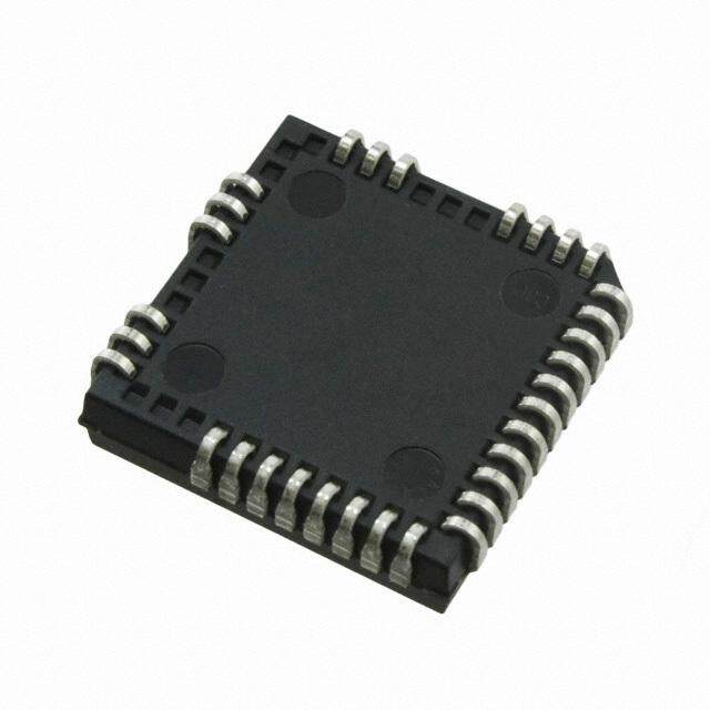
| 描述 | IC MOSFET DVR 3A DUAL HS 8SOIC门驱动器 3A Dual MOSFET Drvr |
| 产品分类 | PMIC - MOSFET,电桥驱动器 - 外部开关集成电路 - IC |
| 品牌 | Microchip Technology |
| 产品手册 | |
| 产品图片 |
|
| rohs | 符合RoHS无铅 / 符合限制有害物质指令(RoHS)规范要求 |
| 产品系列 | 电源管理 IC,门驱动器,Microchip Technology TC4424AVOA- |
| 数据手册 | http://www.microchip.com/mymicrochip/filehandler.aspx?ddocname=en026002http://www.microchip.com/mymicrochip/filehandler.aspx?ddocname=en027108 |
| 产品型号 | TC4424AVOA |
| PCN组件/产地 | http://www.microchip.com/mymicrochip/NotificationDetails.aspx?id=5774&print=view |
| PCN设计/规格 | http://www.microchip.com/mymicrochip/NotificationDetails.aspx?id=5704&print=view |
| 上升时间 | 35 ns |
| 下降时间 | 35 ns |
| 产品 | MOSFET Gate Drivers |
| 产品目录页面 | |
| 产品种类 | 门驱动器 |
| 供应商器件封装 | 8-SOIC N |
| 包装 | 管件 |
| 商标 | Microchip Technology |
| 安装类型 | 表面贴装 |
| 安装风格 | SMD/SMT |
| 封装 | Tube |
| 封装/外壳 | 8-SOIC(0.154",3.90mm 宽) |
| 封装/箱体 | SOIC-8 |
| 工作温度 | -40°C ~ 125°C |
| 工厂包装数量 | 100 |
| 延迟时间 | 40ns |
| 最大功率耗散 | 470 mW |
| 最大工作温度 | + 125 C |
| 最小工作温度 | - 40 C |
| 标准包装 | 100 |
| 激励器数量 | 2 Driver |
| 电压-电源 | 4.5 V ~ 18 V |
| 电流-峰值 | 4.5A |
| 电源电压-最大 | 18 V |
| 电源电压-最小 | 4.5 V |
| 电源电流 | 0.25 mA |
| 类型 | Non-Inverting |
| 输入类型 | 非反相 |
| 输出数 | 2 |
| 输出端数量 | 2 |
| 配置 | Non-Inverting |
| 配置数 | 2 |
| 高压侧电压-最大值(自举) | - |


- 商务部:美国ITC正式对集成电路等产品启动337调查
- 曝三星4nm工艺存在良率问题 高通将骁龙8 Gen1或转产台积电
- 太阳诱电将投资9.5亿元在常州建新厂生产MLCC 预计2023年完工
- 英特尔发布欧洲新工厂建设计划 深化IDM 2.0 战略
- 台积电先进制程称霸业界 有大客户加持明年业绩稳了
- 达到5530亿美元!SIA预计今年全球半导体销售额将创下新高
- 英特尔拟将自动驾驶子公司Mobileye上市 估值或超500亿美元
- 三星加码芯片和SET,合并消费电子和移动部门,撤换高东真等 CEO
- 三星电子宣布重大人事变动 还合并消费电子和移动部门
- 海关总署:前11个月进口集成电路产品价值2.52万亿元 增长14.8%


PDF Datasheet 数据手册内容提取
TC4423A/TC4424A/TC4425A 3A Dual High-Speed Power MOSFET Drivers Features General Description • High Peak Output Current: 4.5A (typical) The TC4423A/TC4424A/TC4425A devices are a family • Wide Input Supply Voltage Operating Range: of dual-output 3A buffers/MOSFET drivers. These devices are improved versions of the earlier TC4423/ - 4.5V to 18V TC4424/TC4425 dual-output 3A driver family. This • High Capacitive Load Drive Capability: improved version features higher peak output current - 1800pF in 12ns drive capability, lower shoot-throught current, matched • Short Delay Times: 40ns (typical) rise/fall times and propagation delay times. The • Matched Rise/Fall Times TC4423A/TC4424A/TC4425A devices are pin- • Low Supply Current: compatible with the existing TC4423/TC4424/TC4425 family. An 8-pin SOIC package option has been added - With Logic ‘1’ Input – 1.0mA (maximum) to the family. The 8-pin DFN package option offers - With Logic ‘0’ Input – 150µA (maximum) increased power dissipation capability for driving • Low Output Impedance: 2.5Ω (typical) heavier capacitive or resistive loads. • Latch-Up Protected: Will Withstand 1.5A Reverse The TC4423A/TC4424A/TC4425A MOSFET drivers Current can easily charge and discharge 1800pF gate • Logic Input Will Withstand Negative Swing Up To capacitance in under 20 ns, provide low enough 5V impedances in both the on and off states to ensure the • Pin compatible with the TC4423/TC4424/TC4425 MOSFET’s intended state will not be affected, even by and TC4426A/TC4427A/TC4428A devices large transients. • Space-saving 8-Pin 150 mil body SOIC and 8-Pin The TC4423A/TC4424A/TC4425A inputs may be 6x5 DFN Packages driven directly from either TTL or CMOS (2.4V to 18V). In addition, the 300 mV of built-in hysteresis provides Applications noise immunity and allows the device to be driven from slow rising or falling waveforms. • Switch Mode Power Supplies The TC4423A/TC4424A/TC4425A dual-output 3A • Pulse Transformer Drive MOSFET driver family is offerd with a -40oC to +125oC • Line Drivers temperature rating, making it useful in any wide • Direct Drive of Small DC Motors temperature range application. Package Types 8-Pin PDIP/SOIC TC4423ATC4424A TC4425A 16-Pin SOIC (Wide) TC4423ATC4424ATC4425A NC 1 8 NC NC NC NC 1 16 NC NC NC IN A 2TC4423A 7 OUT A OUT A OUT A IN A 2 15 OUT A OUT A OUT A GND 3TC4424A 6 VDD VDD VDD NC 3 TC4423A 14 OUT A OUT A OUT A IN B 4TC4425A 5 OUT B OUT B OUT B GND 4 TC4424A 13 VDD VDD VDD GND 5 TC4425A 12 VDD VDD VDD NC 6 11 OUT B OUT B OUT B 8-Pin 6x5 DFN (1) TC4423A TC4424A TC4425A IN B 7 10 OUT B OUT B OUT B NC 8 9 NC NC NC NC 1 8 NC NC NC TC4423A IN A 2 7 OUT A OUT A OUT A TC4424A GND 3 TC4425A 6 VDD VDD VDD IN B 4 5 OUT B OUT B OUT B Note1: Exposed pad of the DFN package is electrically isolated. 2: Duplicate pins must both be connected for proper operation. © 2007 Microchip Technology Inc. DS21998B-page 1
TC4423A/TC4424A/TC4425A Functional Block Diagram(1) V DD Inverting 750µA 300mV Output Non-inverting Input Effective 4.7V Input C = 20pF TC44 23A Dual Inverting (Each Input) TC44 24A Dual Non-inverting TC4425A Inverting / Non-inverting GND Note1: Unused inputs should be grounded. DS21998B-page 2 © 2007 Microchip Technology Inc.
TC4423A/TC4424A/TC4425A 1.0 ELECTRICAL † Notice: Stresses above those listed under "Maximum Ratings" may cause permanent damage to the device. This is CHARACTERISTICS a stress rating only and functional operation of the device at those or any other conditions above those indicated in the Absolute Maximum Ratings † operational sections of this specification is not intended. Exposure to maximum rating conditions for extended periods Supply Voltage................................................................+20V may affect device reliability. Input Voltage, IN A or IN B..........(V + 0.3V) to (GND – 5V) DD Package Power Dissipation (T =50°C) A 8L PDIP.......................................................................1.2W 8L SOIC.................................................................... 0.61W 16L SOIC.....................................................................1.1W 8L DFN.................................................................... Note3 DC CHARACTERISTICS (NOTE 2) Electrical Specifications: Unless otherwise indicated, T = +25°C, with 4.5V ≤ V ≤ 18V. A DD Parameters Sym Min Typ Max Units Conditions Input Logic ‘1’, High Input Voltage VIH 2.4 1.5 — V Logic ‘0’, Low Input Voltage VIL — 1.3 0.8 V Input Current I –1 — 1 µA 0V ≤ V ≤ V IN IN DD Input Voltage V -5 — V +0.3 V IN DD Output High Output Voltage V V – 0.025 — — V DC Test OH DD Low Output Voltage V — — 0.025 V DC Test OL Output Resistance, High R — 2.2 3.0 Ω I = 10mA, V = 18V OH OUT DD Output Resistance, Low R — 2.8 3.5 Ω I = 10mA, V = 18V OL OUT DD Peak Output Current I — 4.5 — A 10V≤ V ≤18V (Note 2) PK DD Latch-Up Protection With- I — >1.5 — A Duty cycle ≤ 2%, t ≤ 300µsec. REV stand Reverse Current Switching Time (Note1) Rise Time t — 12 21 ns Figure4-1, Figure4-2, R C = 1800pF L Fall Time t — 12 21 ns Figure4-1, Figure4-2, F C = 1800pF L Delay Time t — 40 48 ns Figure4-1, Figure4-2, D1 C = 1800pF L Delay Time t — 41 48 ns Figure4-1, Figure4-2, D2 C = 1800pF L Power Supply Supply Voltage V 4.5 — 18 V DD Power Supply Current I — 1.0 2.0 mA V = 3V (Both inputs) S IN I — 0.15 0.25 mA V = 0V (Both inputs) S IN Note 1: Switching times ensured by design. 2: Tested during characterization, not production tested. 3: Package power dissipation is dependent on the copper pad area on the PCB. © 2007 Microchip Technology Inc. DS21998B-page 3
TC4423A/TC4424A/TC4425A DC CHARACTERISTICS (OVER OPERATING TEMPERATURE RANGE) Electrical Specifications: Unless otherwise indicated, operating temperature range with 4.5V ≤ V ≤ 18V. DD Parameters Sym Min Typ Max Units Conditions Input Logic ‘1’, High Input Voltage VIH 2.4 — — V Logic ‘0’, Low Input Voltage VIL — — 0.8 V Input Current I –10 — +10 µA 0V ≤ V ≤ V IN IN DD Output High Output Voltage V V – 0.025 — — V OH DD Low Output Voltage V — — 0.025 V OL Output Resistance, High R — 3.1 6 Ω I = 10mA, V = 18V OH OUT DD Output Resistance, Low R — 3.7 7 Ω I = 10mA, V = 18V OL OUT DD Switching Time (Note1) Rise Time t — 20 31 ns Figure4-1, Figure4-2, R C = 1800pF L Fall Time t — 22 31 ns Figure4-1, Figure4-2, F C = 1800pF L Delay Time t — 50 66 ns Figure4-1, Figure4-2, D1 C = 1800pF L Delay Time t — 50 66 ns Figure4-1, Figure4-2, D2 C = 1800pF L Power Supply Power Supply Current I — 2.0 3.0 mA V = 3V (Both inputs) S IN — 0.2 0.3 V = 0V (Both inputs) IN Note 1: Switching times ensured by design. TEMPERATURE CHARACTERISTICS Electrical Specifications: Unless otherwise noted, all parameters apply with 4.5V ≤ V ≤ 18V. DD Parameters Sym Min Typ Max Units Conditions Temperature Ranges Specified Temperature Range (V) T –40 — +125 °C A Maximum Junction Temperature T — — +150 °C J Storage Temperature Range T –65 — +150 °C A Package Thermal Resistances Thermal Resistance, 8L-6x5 DFN θ — 33.2 — °C/W Typical four-layer board with JA vias to ground plane Thermal Resistance, 8L-PDIP θ — 84.6 — °C/W JA Thermal Resistance, 8L-SOIC θ — 163 — °C/W JA Thermal Resistance, 16L-SOIC θ — 90 — °C/W JA DS21998B-page 4 © 2007 Microchip Technology Inc.
TC4423A/TC4424A/TC4425A 2.0 TYPICAL PERFORMANCE CURVES Note: The graphs and tables provided following this note are a statistical summary based on a limited number of samples and are provided for informational purposes only. The performance characteristics listed herein are not tested or guaranteed. In some graphs or tables, the data presented may be outside the specified operating range (e.g., outside specified power supply range) and therefore outside the warranted range. Note: Unless otherwise indicated, T = +25°C with 4.5V <= V <= 18V. A DD 80 80 70 70 4700 pF 60 4,700 pF 60 3300 pF s) 3,300 pF s) e (n 50 1,800 pF e (n 50 m 40 m 40 1800 pF Ti 1,000 pF Ti se 30 all 30 Ri 20 F 20 10 470 pF 10 1000 pF 470 pF 0 0 4 6 8 10 12 14 16 18 4 6 8 10 12 14 16 18 Supply Voltage (V) Supply Voltage (V) FIGURE 2-1: Rise Time vs. Supply FIGURE 2-4: Fall Time vs. Supply Voltage. Voltage. 60 70 50 60 5V me (ns) 3400 5V 10V me (ns) 4500 10V Rise Ti 20 Fall Ti 2300 15V 15V 10 10 0 0 100 1000 10000 100 1000 10000 Capacitive Load (pF) Capacitive Load (pF) FIGURE 2-2: Rise Time vs. Capacitive FIGURE 2-5: Fall Time vs. Capacitive Load. Load. 24 145 ns) 122802 CLOAD = 18t0FA0L LpF Delay (ns) 110255 tD1 CLOAD =V D1D8 0=0 1 p2FV e ( n 85 m 16 o Ti 14 tRISE agati 65 p 12 Pro 45 tD2 10 25 -40 -25 -10 5 20 35 50 65 80 95 110125 2 3 4 5 6 7 8 9 10 Temperature (oC) Input Amplitude (V) FIGURE 2-3: Rise and Fall Times vs. FIGURE 2-6: Propagation Delay vs. Input Temperature. Amplitude. © 2007 Microchip Technology Inc. DS21998B-page 5
TC4423A/TC4424A/TC4425A Typical Performance Curves (Continued) Note: Unless otherwise indicated, T = +25°C with 4.5V <= V <= 18V. A DD 100 70 y (ns) 8900 tD1 CLOAD = 1800 pF y (ns) 6605 CVVDILNOD = A=D 5 1=V8 1V800 pF tD2 Dela 70 tD2 Dela 55 ation 60 ation 4550 tD1 pag 50 pag 40 o o Pr 40 Pr 35 30 30 4 6 8 10 12 14 16 18 -40 -25 -10 5 20 35 50 65 80 95 110 125 Supply Voltage (V) Temperature (oC) FIGURE 2-7: Propagation Delay Time vs. FIGURE 2-10: Propagation Delay Time vs. Supply Voltage. Temperature. 0.5 0.5 A) VDD = 18V A) VDD = 18V m 0.4 m 0.4 nt ( nt ( Both Inputs = 1 urre 0.3 Both Inputs = 1 urre 0.3 C C nt 0.2 nt 0.2 e e uiesc 0.1 Both Inputs = 0 uiesc 0.1 Both Inputs = 0 Q Q 0 0 4 6 8 10 12 14 16 18 -40 -25 -10 5 20 35 50 65 80 95 110 125 Supply Voltage (V) Temperature (oC) FIGURE 2-8: Quiescent Current vs. FIGURE 2-11: Quiescent Current vs. Supply Voltage. Temperature. 7 8 VIN = 5V (TC4424A) VIN = 0V (TC4424A) 6 TJ = 150oC VIN = 0V (TC4423A) 7 TJ = 150oC VIN = 5V (TC4423A) ):: 5 ):: 6 R (OUT-LO 34 TJ = 25oC R (OUT-HI 45 TJ = 25oC 2 3 1 2 4 6 8 10 12 14 16 18 4 6 8 10 12 14 16 18 Supply Voltage (V) Supply Voltage (V) FIGURE 2-9: Output Resistance (Output FIGURE 2-12: Output Resistance (Output Low) vs. Supply Voltage. High) vs. Supply Voltage. DS21998B-page 6 © 2007 Microchip Technology Inc.
TC4423A/TC4424A/TC4425A Typical Performance Curves (Continued) Note: Unless otherwise indicated, T = +25°C with 4.5V <= V <= 18V. A DD 120 100 VDD = 18V 650 kHz 90 VDD = 18V 10,000 pF mA) 100 50 kHz mA) 80 4,700 pF ent ( 80 100 kHz ent ( 6700 470 pF urr 60 urr 50 C C 40 1,800 pF pply 40 400 kHz 200 kHz pply 30 1,000 pF Su 20 Su 20 10 100 pF 0 0 100 1000 10000 10 100 1000 Capacitive Load (pF) Frequency (kHz) FIGURE 2-13: Supply Current vs. FIGURE 2-16: Supply Current vs. Capacitive Load. Frequency. 140 140 VDD = 12V 2 MHz VDD = 12V 4,700 pF 120 120 A) 100 kHz 200 kHz A) 10,000 pF m 100 m 100 ent ( 80 ent ( 80 1,800 pF ply Curr 4600 500 kHz ply Curr 4600 147,000 p0 FpF p p Su 20 1 MHz Su 20 100 pF 0 0 100 1000 10000 10 100 1000 10000 Capacitive Load (pF) Frequency (kHz) FIGURE 2-14: Supply Current vs. FIGURE 2-17: Supply Current vs. Capacitive Load. Frequency. 120 140 A) 100 VDD = 6V 3.5 MHz 2 MHz A) 120 VDD = 6V 4,700 pF m m 100 nt ( 80 100 kHz 1 MHz nt ( e e 80 urr 60 200 kHz urr 1,800 pF C C 60 ply 40 500 kHz ply 40 1,000 pF p p 10,000 pF Su 20 Su 20 100 pF 470 pF 0 0 100 1000 10000 10 100 1000 10000 100000 Capacitive Load (pF) Frequency (kHz) FIGURE 2-15: Supply Current vs. FIGURE 2-18: Supply Current vs. Capacitive Load. Frequency. © 2007 Microchip Technology Inc. DS21998B-page 7
TC4423A/TC4424A/TC4425A Typical Performance Curves (Continued) Note: Unless otherwise indicated, T = +25°C with 4.5V <= V <= 18V. A DD 11.000E--606 c) e s y (A* 11.000E--707 g er n E ver 11.000E--808 o s s o Cr 11.000E--909 4 6 8 10 12 14 16 18 Supply Voltage (V) Note: The values on this graph represents the loss seen by both drivers in a package during one complete cycle. For a single driver, divide the stated values by 2. For a single transition of a single driver, divide the stated value by 4. FIGURE 2-19: Crossover Energy vs. Supply Voltage. DS21998B-page 8 © 2007 Microchip Technology Inc.
TC4423A/TC4424A/TC4425A 3.0 PIN DESCRIPTIONS The descriptions of the pins are listed in Table3-1. TABLE 3-1: PIN FUNCTION TABLE (1) 16-Pin 8-Pin 8-Pin PDIP SOIC Symbol Description DFN (Wide) 1 1 1 NC No connection 2 2 2 IN A Input A — — 3 NC No connection 3 3 4 GND Ground — — 5 GND Ground — — 6 NC No connection 4 4 7 IN B Input B — — 8 NC No connection — — 9 NC No connection 5 5 10 OUT B Output B — — 11 OUT B Output B 6 6 12 V Supply input DD — — 13 V Supply input DD 7 7 14 OUT A Output A — — 15 OUT A Output A 8 8 16 NC No connection — PAD — NC Exposed Metal Pad Note 1: Duplicate pins must be connected for proper operation. 3.1 Inputs A and B 3.4 Ground (GND) Inputs A and B are TTL/CMOS compatible inputs that Ground is the device return pin. The ground pin should control outputs A and B, respectively. These inputs have a low-impedance connection to the bias supply have 300mV of hysteresis between the high and low source return. High peak currents will flow out the input levels, allowing them to be driven from slow rising ground pin when the capacitive load is being and falling signals, and to provide noise immunity. discharged. 3.2 Outputs A and B 3.5 Exposed Metal Pad Outputs A and B are CMOS push-pull outputs that are The exposed metal pad of the DFN package is not capable of sourcing and sinking 3A peaks of current internally connected to any potential. Therefore, this (V = 18V). The low output impedance ensures the pad can be connected to a ground plane or other DD gate of the external MOSFET will stay in the intended copper plane on a printed circuit board to aid in heat state even during large transients. These outputs also removal from the package. have a reverse current latch-up rating of 1.5A. 3.3 Supply Input (V ) DD V is the bias supply input for the MOSFET driver and DD has a voltage range of 4.5V to 18V. This input must be decoupled to ground with a local ceramic capacitor. This bypass capacitor provides a localized low- impedance path for the peak currents that are to be provided to the load. © 2007 Microchip Technology Inc. DS21998B-page 9
TC4423A/TC4424A/TC4425A 4.0 APPLICATIONS INFORMATION V = 18V V = 18V DD DD 1µF 0.1µF 1µF 0.1µF WIMA Ceramic WIMA Ceramic MKS-2 MKS-2 Input 1 Output Input 1 Output CL = 1800pF CL = 1800pF 2 2 TC4423A TC4424A (1/2 TC4425A) (1/2 TC4425A) Input: 100kHz, Input: 100kHz, square wave, square wave, tRISE = tFALL ≤ 10ns tRISE = tFALL ≤ 10ns +5V 90% +5V 90% Input Input 10% 0V 10% t t 0V D1 D2 t t 18V 90% F R 90% 18V tD190% tD2 90% Output Output tR tF 0V 10% 10% 0V 10% 10% FIGURE 4-1: Inverting Driver Switching FIGURE 4-2: Non-inverting Driver Time. Switching Time. DS21998B-page 10 © 2007 Microchip Technology Inc.
TC4423A/TC4424A/TC4425A 5.0 PACKAGING INFORMATION 5.1 Package Marking Information (Not to Scale) 8-Lead DFN (6x5) Example: XXXXXXX TC4423A XXXXXXX VMF^e^3 XXYYWW 0520 NNN 256 8-Lead PDIP (300 mil) Example: XXXXXXXX TC4423AV XXXXXNNN PA^e^3256 YYWW 0520 8-Lead SOIC (150 mil) Example: XXXXXXXX TC4423AV XXXXYYWW OA^e^30520 NNN 256 16-Lead SOIC (300 mil) Example: XXXXXXXXXXX TC4423A XXXXXXXXXXX VOE^e^3 XXXXXXXXXXX YYWWNNN 0420256 Legend: XX...X Customer-specific information Y Year code (last digit of calendar year) YY Year code (last 2 digits of calendar year) WW Week code (week of January 1 is week ‘01’) NNN Alphanumeric traceability code e3 Pb-free JEDEC designator for Matte Tin (Sn) * This package is Pb-free. The Pb-free JEDEC designator ( e 3 ) can be found on the outer packaging for this package. Note: In the event the full Microchip part number cannot be marked on one line, it will be carried over to the next line, thus limiting the number of available characters for customer-specific information. © 2007 Microchip Technology Inc. DS21998B-page 11
TC4423A/TC4424A/TC4425A 8-Lead Plastic Dual Flat, No Lead Package (MF) – 6x5 mm Body [DFN-S] PUNCH SINGULATED Note: For the most current package drawings, please see the Microchip Packaging Specification located at http://www.microchip.com/packaging D e D1 b L N N K E E2 E1 EXPOSED PAD NOTE 1 1 2 2 1 NOTE 1 D2 TOP VIEW BOTTOM VIEW φ A A2 A1 A3 NOTE 2 Units MILLIMETERS Dimension Limits MIN NOM MAX Number of Pins N 8 Pitch e 1.27 BSC Overall Height A – 0.85 1.00 Molded Package Thickness A2 – 0.65 0.80 Standoff A1 0.00 0.01 0.05 Base Thickness A3 0.20 REF Overall Length D 4.92 BSC Molded Package Length D1 4.67 BSC Exposed Pad Length D2 3.85 4.00 4.15 Overall Width E 5.99 BSC Molded Package Width E1 5.74 BSC Exposed Pad Width E2 2.16 2.31 2.46 Contact Width b 0.35 0.40 0.47 Contact Length L 0.50 0.60 0.75 Contact-to-Exposed Pad K 0.20 – – Model Draft Angle Top φ – – 12° Notes: 1. Pin 1 visual index feature may vary, but must be located within the hatched area. 2. Package may have one or more exposed tie bars at ends. 3. Dimensioning and tolerancing per ASME Y14.5M. BSC: Basic Dimension. Theoretically exact value shown without tolerances. REF: Reference Dimension, usually without tolerance, for information purposes only. MicrochipTechnologyDrawingC04-113B DS21998B-page 12 © 2007 Microchip Technology Inc.
TC4423A/TC4424A/TC4425A 8-Lead Plastic Dual In-Line (PA) – 300 mil Body [PDIP] Note: For the most current package drawings, please see the Microchip Packaging Specification located at http://www.microchip.com/packaging N NOTE 1 E1 1 2 3 D E A A2 L A1 c e eB b1 b Units INCHES Dimension Limits MIN NOM MAX Number of Pins N 8 Pitch e .100 BSC Top to Seating Plane A – – .210 Molded Package Thickness A2 .115 .130 .195 Base to Seating Plane A1 .015 – – Shoulder to Shoulder Width E .290 .310 .325 Molded Package Width E1 .240 .250 .280 Overall Length D .348 .365 .400 Tip to Seating Plane L .115 .130 .150 Lead Thickness c .008 .010 .015 Upper Lead Width b1 .040 .060 .070 Lower Lead Width b .014 .018 .022 Overall Row Spacing § eB – – .430 Notes: 1. Pin 1 visual index feature may vary, but must be located with the hatched area. 2. § Significant Characteristic. 3. Dimensions D and E1 do not include mold flash or protrusions. Mold flash or protrusions shall not exceed .010" per side. 4. Dimensioning and tolerancing per ASME Y14.5M. BSC: Basic Dimension. Theoretically exact value shown without tolerances. MicrochipTechnologyDrawingC04-018B © 2007 Microchip Technology Inc. DS21998B-page 13
TC4423A/TC4424A/TC4425A 8-Lead Plastic Small Outline (OA) – Narrow, 3.90 mm Body [SOIC] Note: For the most current package drawings, please see the Microchip Packaging Specification located at http://www.microchip.com/packaging D e N E E1 NOTE 1 1 2 3 b h α h c A A2 φ A1 L L1 β Units MILLIMETERS Dimension Limits MIN NOM MAX Number of Pins N 8 Pitch e 1.27 BSC Overall Height A – – 1.75 Molded Package Thickness A2 1.25 – – Standoff § A1 0.10 – 0.25 Overall Width E 6.00 BSC Molded Package Width E1 3.90 BSC Overall Length D 4.90 BSC Chamfer (optional) h 0.25 – 0.50 Foot Length L 0.40 – 1.27 Footprint L1 1.04 REF Foot Angle φ 0° – 8° Lead Thickness c 0.17 – 0.25 Lead Width b 0.31 – 0.51 Mold Draft Angle Top α 5° – 15° Mold Draft Angle Bottom β 5° – 15° Notes: 1. Pin 1 visual index feature may vary, but must be located within the hatched area. 2. § Significant Characteristic. 3. Dimensions D and E1 do not include mold flash or protrusions. Mold flash or protrusions shall not exceed 0.15 mm per side. 4. Dimensioning and tolerancing per ASME Y14.5M. BSC: Basic Dimension. Theoretically exact value shown without tolerances. REF: Reference Dimension, usually without tolerance, for information purposes only. MicrochipTechnologyDrawingC04-057B DS21998B-page 14 © 2007 Microchip Technology Inc.
TC4423A/TC4424A/TC4425A 16-Lead Plastic Small Outline (OE) – Wide, 7.50 mm Body [SOIC] Note: For the most current package drawings, please see the Microchip Packaging Specification located at http://www.microchip.com/packaging D N E E1 NOTE 1 1 2 3 e b h α h c φ A A2 L A1 β L1 Units MILLIMETERS Dimension Limits MIN NOM MAX Number of Pins N 16 Pitch e 1.27 BSC Overall Height A – – 2.65 Molded Package Thickness A2 2.05 – – Standoff § A1 0.10 – 0.30 Overall Width E 10.30 BSC Molded Package Width E1 7.50 BSC Overall Length D 10.30 BSC Chamfer (optional) h 0.25 – 0.75 Foot Length L 0.40 – 1.27 Footprint L1 1.40 REF Foot Angle φ 0° – 8° Lead Thickness c 0.20 – 0.33 Lead Width b 0.31 – 0.51 Mold Draft Angle Top α 5° – 15° Mold Draft Angle Bottom β 5° – 15° Notes: 1. Pin 1 visual index feature may vary, but must be located within the hatched area. 2. § Significant Characteristic. 3. Dimensions D and E1 do not include mold flash or protrusions. Mold flash or protrusions shall not exceed 0.15 mm per side. 4. Dimensioning and tolerancing per ASME Y14.5M. BSC: Basic Dimension. Theoretically exact value shown without tolerances. REF: Reference Dimension, usually without tolerance, for information purposes only. MicrochipTechnologyDrawingC04-102B © 2007 Microchip Technology Inc. DS21998B-page 15
TC4423A/TC4424A/TC4425A NOTES: DS21998B-page 16 © 2007 Microchip Technology Inc.
TC4423A/TC4424A/TC4425A APPENDIX A: REVISION HISTORY Revision B (April 2007) • Correct numerous errors throughout document. • Page 3: Added Package Power Dissipation information about DC Characteristic Table. • Page 3: Added Note 3 to DC Characteristic Table. • Page 4: Changed Thermal Resistance for 8L-PDIP device from 125 to 84.6. Changed Thermal Resistance for 8L-SOIC from 155 to 163. • Page 12: Updated Package Outline Drawing. • Page 13: Updated Package Outline Drawing. • Page 14: Updated Package Outline Drawing. • Page 15: Added 16-Lead SOIC Package Outline Drawing • Page 17: Updated Revision History. Revision A (June 2006) • Original Release of this Document. © 2007 Microchip Technology Inc. DS21998B-page 17
TC4423A/TC4424A/TC4425A NOTES: DS21998B-page 18 © 2007 Microchip Technology Inc.
TC4423A/TC4424A/TC4425A PRODUCT IDENTIFICATION SYSTEM To order or obtain information, e.g., on pricing or delivery, refer to the factory or the listed sales office. PART NO. X XX XXX Examples: a) TC4423AVOA: 3A Dual Inverting Device Temperature Package Tape & Reel MOSFET Driver, Range 8LD SOIC package. b) TC4423AVPA: 3A Dual Inverting Device: TC4423A: 3A Dual MOSFET Driver, Inverting MOSFET Driver, TC4424A: 3A Dual MOSFET Driver, Non-Inverting 8LD PDIP package. TC4425A: 3A Dual MOSFET Driver, Complementary c) TC4423AVMF: 3A Dual Inverting MOSFET Driver, Temperature Range: V = -40°C to +125°C 8LD DFN package. d) TC4423AVOE: 3A Dual Inverting MOSFET Driver, Package: * MF = Dual, Flat, No-Lead (6x5 mm Body), 8-lead 16LD SOIC package. MF713 = Dual, Flat, No-Lead (6x5 mm Body), 8-lead (Tape and Reel) OA = Plastic SOIC (150 mil Body), 8-Lead a) TC4424AVOA713: 3A Dual Non-Inverting, OA713 = Plastic SOIC (150 mil Body), 8-Lead MOSFET Driver, (Tape and Reel) 8LD SOIC package, OE = Plastic SOIC (Wide Body), 16-lead Tape and Reel. OE713 = Plastic SOIC (Wide Body), 16-lead (Tape and Reel) b) TC4424AVPA: 3A Dual Non-Inverting, PA = Plastic DIP, (300 mil body), 8-lead MOSFET Driver, * All package offerings are Pb Free (Lead Free) 8LD PDIP package. a) TC4425AVOA: 3A Dual Complementary, MOSFET Driver, 8LD SOIC package. b) TC4425AVPA: 3A Dual Complementary, MOSFET Driver, 8LD PDIP package. c) TC4425AVOE713: 3A Dual Complementary, MOSFET Driver, 16LD SOIC package, Tape and Reel. © 2007 Microchip Technology Inc. DS21998B-page 19
TC4423A/TC4424A/TC4425A NOTES: DS21998B-page 20 © 2007 Microchip Technology Inc.
Note the following details of the code protection feature on Microchip devices: • Microchip products meet the specification contained in their particular Microchip Data Sheet. • Microchip believes that its family of products is one of the most secure families of its kind on the market today, when used in the intended manner and under normal conditions. • There are dishonest and possibly illegal methods used to breach the code protection feature. All of these methods, to our knowledge, require using the Microchip products in a manner outside the operating specifications contained in Microchip’s Data Sheets. Most likely, the person doing so is engaged in theft of intellectual property. • Microchip is willing to work with the customer who is concerned about the integrity of their code. • Neither Microchip nor any other semiconductor manufacturer can guarantee the security of their code. Code protection does not mean that we are guaranteeing the product as “unbreakable.” Code protection is constantly evolving. We at Microchip are committed to continuously improving the code protection features of our products. Attempts to break Microchip’s code protection feature may be a violation of the Digital Millennium Copyright Act. If such acts allow unauthorized access to your software or other copyrighted work, you may have a right to sue for relief under that Act. Information contained in this publication regarding device Trademarks applications and the like is provided only for your convenience The Microchip name and logo, the Microchip logo, Accuron, and may be superseded by updates. It is your responsibility to dsPIC, KEELOQ, KEELOQ logo, microID, MPLAB, PIC, ensure that your application meets with your specifications. PICmicro, PICSTART, PROMATE, PowerSmart, rfPIC, and MICROCHIP MAKES NO REPRESENTATIONS OR SmartShunt are registered trademarks of Microchip WARRANTIES OF ANY KIND WHETHER EXPRESS OR Technology Incorporated in the U.S.A. and other countries. IMPLIED, WRITTEN OR ORAL, STATUTORY OR OTHERWISE, RELATED TO THE INFORMATION, AmpLab, FilterLab, Linear Active Thermistor, Migratable INCLUDING BUT NOT LIMITED TO ITS CONDITION, Memory, MXDEV, MXLAB, PS logo, SEEVAL, SmartSensor QUALITY, PERFORMANCE, MERCHANTABILITY OR and The Embedded Control Solutions Company are FITNESS FOR PURPOSE. Microchip disclaims all liability registered trademarks of Microchip Technology Incorporated arising from this information and its use. Use of Microchip in the U.S.A. devices in life support and/or safety applications is entirely at Analog-for-the-Digital Age, Application Maestro, CodeGuard, the buyer’s risk, and the buyer agrees to defend, indemnify and dsPICDEM, dsPICDEM.net, dsPICworks, ECAN, hold harmless Microchip from any and all damages, claims, ECONOMONITOR, FanSense, FlexROM, fuzzyLAB, suits, or expenses resulting from such use. No licenses are In-Circuit Serial Programming, ICSP, ICEPIC, Mindi, MiWi, conveyed, implicitly or otherwise, under any Microchip MPASM, MPLAB Certified logo, MPLIB, MPLINK, PICkit, intellectual property rights. PICDEM, PICDEM.net, PICLAB, PICtail, PowerCal, PowerInfo, PowerMate, PowerTool, REAL ICE, rfLAB, rfPICDEM, Select Mode, Smart Serial, SmartTel, Total Endurance, UNI/O, WiperLock and ZENA are trademarks of Microchip Technology Incorporated in the U.S.A. and other countries. SQTP is a service mark of Microchip Technology Incorporated in the U.S.A. All other trademarks mentioned herein are property of their respective companies. © 2007, Microchip Technology Incorporated, Printed in the U.S.A., All Rights Reserved. Printed on recycled paper. Microchip received ISO/TS-16949:2002 certification for its worldwide headquarters, design and wafer fabrication facilities in Chandler and Tempe, Arizona, Gresham, Oregon and Mountain View, California. The Company’s quality system processes and procedures are for its PIC® MCUs and dsPIC® DSCs, KEELOQ® code hopping devices, Serial EEPROMs, microperipherals, nonvolatile memory and analog products. In addition, Microchip’s quality system for the design and manufacture of development systems is ISO 9001:2000 certified. © 2007 Microchip Technology Inc. DS21998B-page 21
WORLDWIDE SALES AND SERVICE AMERICAS ASIA/PACIFIC ASIA/PACIFIC EUROPE Corporate Office Asia Pacific Office India - Bangalore Austria - Wels 2355 West Chandler Blvd. Suites 3707-14, 37th Floor Tel: 91-80-4182-8400 Tel: 43-7242-2244-39 Chandler, AZ 85224-6199 Tower 6, The Gateway Fax: 91-80-4182-8422 Fax: 43-7242-2244-393 Tel: 480-792-7200 Habour City, Kowloon India - New Delhi Denmark - Copenhagen Fax: 480-792-7277 Hong Kong Tel: 91-11-4160-8631 Tel: 45-4450-2828 Technical Support: Tel: 852-2401-1200 Fax: 91-11-4160-8632 Fax: 45-4485-2829 http://support.microchip.com Web Address: Fax: 852-2401-3431 India - Pune France - Paris www.microchip.com Australia - Sydney Tel: 91-20-2566-1512 Tel: 33-1-69-53-63-20 Tel: 61-2-9868-6733 Fax: 33-1-69-30-90-79 Fax: 91-20-2566-1513 Atlanta Fax: 61-2-9868-6755 Germany - Munich Duluth, GA Japan - Yokohama China - Beijing Tel: 49-89-627-144-0 Tel: 678-957-9614 Tel: 81-45-471- 6166 Tel: 86-10-8528-2100 Fax: 49-89-627-144-44 Fax: 678-957-1455 Fax: 81-45-471-6122 Fax: 86-10-8528-2104 Italy - Milan Boston Korea - Gumi Westborough, MA China - Chengdu Tel: 82-54-473-4301 Tel: 39-0331-742611 Tel: 774-760-0087 Tel: 86-28-8665-5511 Fax: 82-54-473-4302 Fax: 39-0331-466781 Fax: 774-760-0088 Fax: 86-28-8665-7889 Korea - Seoul Netherlands - Drunen Chicago China - Fuzhou Tel: 82-2-554-7200 Tel: 31-416-690399 Itasca, IL Tel: 86-591-8750-3506 Fax: 82-2-558-5932 or Fax: 31-416-690340 Tel: 630-285-0071 Fax: 86-591-8750-3521 82-2-558-5934 Spain - Madrid Fax: 630-285-0075 China - Hong Kong SAR Malaysia - Penang Tel: 34-91-708-08-90 Dallas Tel: 852-2401-1200 Tel: 60-4-646-8870 Fax: 34-91-708-08-91 Addison, TX Fax: 852-2401-3431 Fax: 60-4-646-5086 UK - Wokingham Tel: 972-818-7423 China - Qingdao Philippines - Manila Tel: 44-118-921-5869 Fax: 972-818-2924 Tel: 86-532-8502-7355 Tel: 63-2-634-9065 Fax: 44-118-921-5820 Detroit Fax: 86-532-8502-7205 Fax: 63-2-634-9069 Farmington Hills, MI China - Shanghai Singapore Tel: 248-538-2250 Tel: 86-21-5407-5533 Tel: 65-6334-8870 Fax: 248-538-2260 Fax: 86-21-5407-5066 Fax: 65-6334-8850 Kokomo China - Shenyang Taiwan - Hsin Chu Kokomo, IN Tel: 86-24-2334-2829 Tel: 886-3-572-9526 Tel: 765-864-8360 Fax: 86-24-2334-2393 Fax: 886-3-572-6459 Fax: 765-864-8387 China - Shenzhen Taiwan - Kaohsiung Los Angeles Tel: 86-755-8203-2660 Tel: 886-7-536-4818 Mission Viejo, CA Fax: 86-755-8203-1760 Fax: 886-7-536-4803 Tel: 949-462-9523 China - Shunde Taiwan - Taipei Fax: 949-462-9608 Tel: 86-757-2839-5507 Tel: 886-2-2500-6610 Santa Clara Fax: 86-757-2839-5571 Fax: 886-2-2508-0102 Santa Clara, CA China - Wuhan Thailand - Bangkok Tel: 408-961-6444 Tel: 86-27-5980-5300 Tel: 66-2-694-1351 Fax: 408-961-6445 Fax: 86-27-5980-5118 Fax: 66-2-694-1350 Toronto China - Xian Mississauga, Ontario, Tel: 86-29-8833-7250 Canada Fax: 86-29-8833-7256 Tel: 905-673-0699 Fax: 905-673-6509 12/08/06 DS21998B-page 22 © 2007 Microchip Technology Inc.
Mouser Electronics Authorized Distributor Click to View Pricing, Inventory, Delivery & Lifecycle Information: M icrochip: TC4423AVMF TC4423AVMF713 TC4423AVOA TC4423AVOA713 TC4423AVPA TC4424AVMF TC4424AVMF713 TC4424AVOA TC4424AVOA713 TC4424AVPA TC4425AVMF TC4425AVMF713 TC4425AVOA TC4425AVOA713 TC4425AVPA TC4424AVOE713 TC4423AVOE713 TC4424AVOE