ICGOO在线商城 > 集成电路(IC) > PMIC - 栅极驱动器 > TC427EOA
 Datasheet下载
- 型号: TC427EOA
- 制造商: Microchip
- 库位|库存: xxxx|xxxx
- 要求:
| 数量阶梯 | 香港交货 | 国内含税 |
| +xxxx | $xxxx | ¥xxxx |
查看当月历史价格
查看今年历史价格
TC427EOA产品简介:
ICGOO电子元器件商城为您提供TC427EOA由Microchip设计生产,在icgoo商城现货销售,并且可以通过原厂、代理商等渠道进行代购。 TC427EOA价格参考¥5.49-¥5.49。MicrochipTC427EOA封装/规格:PMIC - 栅极驱动器, Low-Side Gate Driver IC Non-Inverting 8-SOIC。您可以下载TC427EOA参考资料、Datasheet数据手册功能说明书,资料中有TC427EOA 详细功能的应用电路图电压和使用方法及教程。
Microchip Technology的TC427EOA是一款PMIC(电源管理集成电路)中的栅极驱动器,主要用于驱动MOSFET或IGBT等功率开关器件。它具有高效、低功耗和高集成度的特点,适用于多种电力电子应用场合。

 应用场景:

1. 电机驱动:
   TC427EOA可以用于驱动电机控制器中的功率开关,如逆变器电路。它可以快速、准确地控制MOSFET或IGBT的开关状态,从而实现高效的电机调速和控制。适用于工业自动化、家用电器(如空调、洗衣机)以及电动汽车等领域。

2. 太阳能逆变器:
   在光伏系统中,TC427EOA可以用于驱动逆变器中的功率开关,将直流电转换为交流电。其高效能和低损耗特性有助于提高系统的整体效率,减少能量损失,适用于住宅和商业太阳能发电系统。

3. 不间断电源(UPS):
   TC427EOA可以用于UPS中的逆变器和充电器电路,确保在市电中断时能够迅速切换到备用电池供电,并保持稳定的输出电压。其快速响应能力和高可靠性使得它非常适合用于数据中心、通信基站等关键设备的电力保障。

4. 电动工具和家电:
   该器件可以用于电动工具(如电钻、割草机)和家电(如吸尘器、风扇)中的无刷直流电机驱动器。通过精确控制功率开关,它可以提高产品的性能和耐用性,同时降低能耗。

5. 电动汽车和混合动力汽车:
   在电动汽车和混合动力汽车中,TC427EOA可以用于驱动主逆变器、辅助逆变器和其他电力电子模块中的功率开关。其紧凑的设计和高集成度有助于减小系统的体积和重量,提升车辆的整体性能。

6. LED照明驱动:
   TC427EOA还可以用于LED照明驱动电路,特别是在需要高频开关的应用中。它能够提供稳定的电流和电压输出,确保LED灯的亮度和色温一致性,适用于路灯、室内照明等场景。

总之,TC427EOA凭借其高效能、低功耗和高集成度的优势,广泛应用于各种电力电子设备中,帮助实现更高效、更可靠的电力转换和控制。
| 参数 | 数值 |
| 产品目录 | 集成电路 (IC)半导体 |
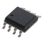
| 描述 | IC MOSFET DVR 1.5A DUAL HS 8SOIC门驱动器 1.5A Dual H-Speed |
| 产品分类 | PMIC - MOSFET,电桥驱动器 - 外部开关集成电路 - IC |
| 品牌 | Microchip Technology |
| 产品手册 | |
| 产品图片 |
|
| rohs | 符合RoHS无铅 / 符合限制有害物质指令(RoHS)规范要求 |
| 产品系列 | 电源管理 IC,门驱动器,Microchip Technology TC427EOA- |
| 数据手册 | http://www.microchip.com/mymicrochip/filehandler.aspx?ddocname=en011463 |
| 产品型号 | TC427EOA |
| PCN组件/产地 | http://www.microchip.com/mymicrochip/NotificationDetails.aspx?id=5774&print=view |
| PCN设计/规格 | http://www.microchip.com/mymicrochip/NotificationDetails.aspx?id=5704&print=view |
| 上升时间 | 30 ns |
| 下降时间 | 30 ns |
| 产品 | MOSFET Gate Drivers |
| 产品目录页面 | |
| 产品种类 | 门驱动器 |
| 供应商器件封装 | 8-SOIC N |
| 包装 | 管件 |
| 商标 | Microchip Technology |
| 安装类型 | 表面贴装 |
| 安装风格 | SMD/SMT |
| 封装 | Tube |
| 封装/外壳 | 8-SOIC(0.154",3.90mm 宽) |
| 封装/箱体 | SOIC-8 |
| 工作温度 | -40°C ~ 85°C |
| 工厂包装数量 | 100 |
| 延迟时间 | 50ns |
| 最大功率耗散 | 470 mW |
| 最大工作温度 | + 85 C |
| 最小工作温度 | - 40 C |
| 标准包装 | 100 |
| 激励器数量 | 2 Driver |
| 电压-电源 | 4.5 V ~ 18 V |
| 电流-峰值 | 1.5A |
| 电源电压-最大 | 16 V |
| 电源电压-最小 | 4.5 V |
| 电源电流 | 8 mA |
| 类型 | Low Side |
| 输入类型 | 非反相 |
| 输出数 | 2 |
| 输出端数量 | 2 |
| 配置 | 低端 |
| 配置数 | 2 |
| 高压侧电压-最大值(自举) | - |


- 商务部:美国ITC正式对集成电路等产品启动337调查
- 曝三星4nm工艺存在良率问题 高通将骁龙8 Gen1或转产台积电
- 太阳诱电将投资9.5亿元在常州建新厂生产MLCC 预计2023年完工
- 英特尔发布欧洲新工厂建设计划 深化IDM 2.0 战略
- 台积电先进制程称霸业界 有大客户加持明年业绩稳了
- 达到5530亿美元!SIA预计今年全球半导体销售额将创下新高
- 英特尔拟将自动驾驶子公司Mobileye上市 估值或超500亿美元
- 三星加码芯片和SET,合并消费电子和移动部门,撤换高东真等 CEO
- 三星电子宣布重大人事变动 还合并消费电子和移动部门
- 海关总署:前11个月进口集成电路产品价值2.52万亿元 增长14.8%


PDF Datasheet 数据手册内容提取
TC426/TC427/TC428 1.5A Dual High-Speed Power MOSFET Drivers Features: Package Type • High-Speed Switching (C = 1000 pF): 30 nsec 8-Pin PDIP/SOIC/CERDIP L • High Peak Output Current: 1.5A NC 1 8 NC • High Output Voltage Swing: IN A 2 7 OUT A 2, 4 7, 5 - VDD -25 mV GND 3 TC426 6 VDD Inverting - GND +25 mV IN B 4 5 OUT B • Low Input Current (Logic ‘0’ or ‘1’): 1 A NC 1 8 NC • TTL/CMOS Input Compatible IN A 2 7 OUT A 2, 4 7, 5 • Available in Inverting and Noninverting GND 3 TC427 6 VDD Noninverting Configurations IN B 4 5 OUT B • Wide Operating Supply Voltage: - 4.5V to 18V NC 1 8 NC 2 7 IN A 2 7 OUT A • Current Consumption: GND 3 TC428 6 VDD 4 5 - Inputs Low – 0.4 mA IN B 4 5 OUT B - Inputs High – 8 mA Complementary • Single Supply Operation NC = No internal connection • Low Output Impedance: 6 General Description: • Pinout Equivalent of DS0026 and MMH0026 • Latch-Up Resistant: Withstands > 500 mA The TC426/TC427/TC428 are dual CMOS high-speed Reverse Current drivers. A TTL/CMOS input voltage level is translated into a rail-to-rail output voltage level swing. The CMOS • ESD Protected: 2 kV output is within 25 mV of ground or positive supply. Applications: The low-impedance, high-current driver outputs swing a 1000 pF load 18V in 30 nsec. The unique current and • Switch Mode Power Supplies voltage drive qualities make the TC426/TC427/TC428 • Pulse Transformer Drive ideal power MOSFET drivers, line drivers, and DC-to- • Clock Line Driver DC converter building blocks. • Coax Cable Driver Input logic signals may equal the power supply voltage. Input current is a low 1 A, making direct interface Device Selection Table toCMOS/bipolar switch-mode power supply control ICs possible, as well as open-collector analog Part Temp. Package Configuration comparators. Number Range Quiescent power supply current is 8 mA maximum. The TC426COA 8-Pin SOIC Inverting 0°C to +70°C TC426CPA 8-Pin PDIP Inverting 0°C to +70°C TC426 requires 1/5 the current of the pin-compatible TC426EOA 8-Pin SOIC Inverting -40°C to +85°C bipolar DS0026 device. This is important in DC-to-DC TC426EPA 8-Pin PDIP Inverting -40°C to +85°C TC426IJA 8-Pin CERDIP Inverting -25°C to +85°C converter applications with power efficiency constraints TC426MJA 8-Pin CERDIP Inverting -55°C to +125°C and high-frequency switch-mode power supply TC427COA 8-Pin SOIC Noninverting 0°C to +70°C applications. Quiescent current is typically 6 mA when TC427CPA 8-Pin PDIP Noninverting 0°C to +70°C driving a 1000 pF load 18V at 100 kHz. TC427EOA 8-Pin SOIC Noninverting -40°C to +85°C TC427EPA 8-Pin PDIP Noninverting -40°C to +85°C The inverting TC426 driver is pin-compatible with the TC427IJA 8-Pin CERDIP Noninverting -25°C to +85°C bipolar DS0026 and MMH0026 devices. The TC427 is TC427MJA 8-Pin CERDIP Noninverting -55°C to +125°C noninverting; the TC428 contains an inverting and non- TC428COA 8-Pin SOIC Complementary 0°C to +70°C TC428CPA 8-Pin PDIP Complementary 0°C to +70°C inverting driver. TC428EOA 8-Pin SOIC Complementary -40°C to +85°C TC428EPA 8-Pin PDIP Complementary -40°C to +85°C Other pin compatible driver families are the TC1426/ TC428IJA 8-Pin CERDIP Complementary -25°C to +85°C TC1427/TC1428, TC4426/TC4427/TC4428 and TC428MJA 8-Pin CERDIP Complementary -55°C to +125°C TC4426A/TC4427A/TC4428A. 2002-2012 Microchip Technology Inc. DS21415D-page 1
TC426/TC427/TC428 Functional Block Diagram + V TC426 ≈500 μ A TC427 TC428 ≈2.5 μ A Noninverting Inverting Output Output (TC427) (TC426) Input GND NOTE: TC428 has one inverting and one noninverting driver. Ground any unused driver input. DS21415D-page 2 2002-2012 Microchip Technology Inc.
TC426/TC427/TC428 1.0 ELECTRICAL *Stresses above those listed under “Absolute CHARACTERISTICS Maximum Ratings” may cause permanent damage to the device. These are stress ratings only and functional operation of the device at these or any other conditions Absolute Maximum Ratings* above those indicated in the operation sections of the specifications is not implied. Exposure to Absolute Supply Voltage.....................................................+20V Maximum Rating conditions for extended periods may Input Voltage, Any Terminal affect device reliability. ...................................V + 0.3V to GND – 0.3V DD Power Dissipation (T 70°C) A PDIP........................................................730 mW CERDIP..................................................800 mW SOIC.......................................................470 mW Derating Factor PDIP.......................................................8 mW/°C CERDIP..............................................6.4 mW/°C SOIC......................................................4 mW/°C Operating Temperature Range C Version........................................0°C to +70°C I Version.......................................-25°C to +85°C E Version......................................-40°C to +85°C M Version...................................-55°C to +125°C Storage Temperature Range..............-65°C to +150°C TC426/TC427/TC428 ELECTRICAL SPECIFICATIONS Electrical Characteristics: T = +25°C with 4.5V V 18V, unless otherwise noted. A DD Symbol Parameter Min Typ Max Units Test Conditions Input V Logic 1, High Input Voltage 2.4 — — V IH V Logic 0, Low Input Voltage — — 0.8 V IL I Input Current -1 — 1 A 0VV V IN IN DD Output V High Output Voltage V – 0.025 — — V OH DD V Low Output Voltage — — 0.025 V OL R High Output Resistance — 10 15 I = 10 mA, V = 18V OH OUT DD R Low Output Resistance — 6 10 I = 10 mA, V = 18V OL OUT DD I Peak Output Current — 1.5 — A PK Switching Time (Note 1) t Rise Time — — 30 nsec Figure3-1, Figure3-2 R t Fall Time — — 30 nsec Figure3-1, Figure3-2 F t Delay Time — — 50 nsec Figure3-1, Figure3-2 D1 t Delay Time — — 75 nsec Figure3-1, Figure3-2 D2 Power Supply I Power Supply Current — — 8 mA V = 3V (Both Inputs) S IN — — 0.4 V = 0V (Both Inputs) IN Note 1: Switching times ensured by design. 2002-2012 Microchip Technology Inc. DS21415D-page 3
TC426/TC427/TC428 TC426/TC427/TC428 ELECTRICAL SPECIFICATIONS (CONTINUED) Electrical Characteristics: Over operating temperature range with 4.5V V 18V, unless otherwise noted. DD Input V Logic 1, High Input Voltage 2.4 — — V IH V Logic 0, Low Input Voltage — — 0.8 V IL I Input Current -10 — 10 A 0VV V IN IN DD Output V High Output Voltage V – 0.025 — — V OH DD V Low Output Voltage — — 0.025 V OL R High Output Resistance — 13 20 I = 10 mA, V = 18V OH OUT DD R Low Output Resistance — 8 15 I = 10 mA, V = 18V OL OUT DD Switching Time (Note 1) t Rise Time — — 60 nsec Figure3-1, Figure3-2 R t Fall Time — — 60 nsec Figure3-1, Figure3-2 F t Delay Time — — 75 nsec Figure3-1, Figure3-2 D1 t Delay Time — — 120 nsec Figure3-1, Figure3-2 D2 Power Supply I Power Supply Current — — 12 mA V = 3V (Both Inputs) S IN — — 0.6 V = 0V (Both Inputs) IN Note 1: Switching times ensured by design. DS21415D-page 4 2002-2012 Microchip Technology Inc.
TC426/TC427/TC428 2.0 PIN DESCRIPTIONS The descriptions of the pins are listed in Table2-1. TABLE 2-1: PIN FUNCTION TABLE Pin No. (8-Pin PDIP, Symbol Description SOIC, CERDIP) 1 NC No Internal Connection. 2 IN A Control Input A, TTL/CMOS compatible logic input. 3 GND Ground. 4 IN B Control Input B, TTL/CMOS compatible logic input. 5 OUT B CMOS totem-pole output. 6 V Supply input, 4.5V to 18V. DD 7 OUT A CMOS totem-pole output. 8 NC No internal Connection. 2002-2012 Microchip Technology Inc. DS21415D-page 5
TC426/TC427/TC428 3.0 APPLICATIONS INFORMATION 3.4 Power Dissipation The supply current vs frequency and supply current 3.1 Supply Bypassing vscapacitive load characteristic curves will aid in determining power dissipation calculations. Charging and discharging large capacitive loads quickly requires large currents. For example, charging The TC426/TC427/TC428 CMOS drivers have greatly a 1000 pF load to 18V in 25 nsec requires an 0.72A reduced quiescent DC power consumption. Maximum current from the device power supply. quiescent current is 8 mA compared to the DS0026 40 mA specification. For a 15V supply, power dissipation To ensure low supply impedance over a wide frequency is typically 40 mW. range, a parallel capacitor combination is recom- mended for supply bypassing. Low-inductance ceramic Two other power dissipation components are: disk capacitors with short lead lengths (< 0.5 in.) should • Output stage AC and DC load power. be used. A 1 F film capacitor in parallel with one or two 0.1 F ceramic disk capacitors normally provides • Transition state power. adequate bypassing. Output stage power is: 3.2 Grounding Po = PDC + PAC = Vo (I ) + f C V 2 DC L S The TC426 and TC428 contain inverting drivers. Where: Ground potential drops developed in common ground impedances from input to output will appear as Vo = DC output voltage negative feedback and degrade switching speed I = DC output load current DC characteristics. f = Switching frequency Individual ground returns for the input and output Vs = Supply voltage circuits or a ground plane should be used. In power MOSFET drive applications the P term is DC negligible. MOSFET power transistors are high-imped- 3.3 Input Stage ance, capacitive input devices. In applications where The input voltage level changes the no-load or resistive loads or relays are driven, the PDC component quiescent supply current. The N-channel MOSFET will normally dominate. input stage transistor drives a 2.5 mA current source The magnitude of P is readily estimated for several AC load. With a logic ‘1’ input, the maximum quiescent cases: supply current is 8 mA. Logic ‘0’ input level signals reduce quiescent current to 0.4 mA maximum. A. B. Minimum power dissipation occurs for logic ‘0’ inputs 1. f = 200 kHZ 1. f = 200 kHz for the TC426/TC427/TC428. Unused driver inputs 2. C =1000 pf 2. C =1000 pf must be connected to V or GND. L L DD 3. Vs = 18V 3. Vs = 15V The drivers are designed with 100 mV of hysteresis. 4. P = 65 mW 4. P = 45 mW This provides clean transitions and minimizes output AC AC stage current spiking when changing states. Input During output level state changes, a current surge will voltage thresholds are approximately 1.5V, making the flow through the series connected N and P channel device TTL compatible over the 4.5V to 18V supply output MOSFETS as one device is turning “ON” while operating range. Input current is less than 1 A over the other is turning “OFF”. The current spike flows only this range. during output transitions. The input levels should not be The TC426/TC427/TC428 may be directly driven by maintained between the logic ‘0’ and logic ‘1’ levels. Unused driver inputs must be tied to ground and the TL494, SG1526/1527, SG1524, SE5560, and similar switch-mode power supply integrated circuits. not be allowed to float. Average power dissipation will be reduced by minimizing input rise times. As shown in the characteristic curves, average supply current is frequency dependent. DS21415D-page 6 2002-2012 Microchip Technology Inc.
TC426/TC427/TC428 VDD = 18V VDD = 18V 1 μ F 0.1 μ F 1 μ F 0.1 μ F Input 1 Output Input 1 Output CL = 1000 pF CL = 1000 pF Input: 100 kHz, 2 2 square wave, Input: 100 kHz, tRISE = tFALL ≤ 10 nsec TC426 tRISEs =q utFaAreL Lw ≤a v1e0, nsec TC427 (1/2 TC428) (1/2 TC428) +5V 90% +5V 90% Input Input 10% 0V 10% tD1 tD2 0V 18V 90% tF tR 90% 18V tD1 90% tD2 90% Output Output tR tF 10% 10% 0V 10% 10% 0V FIGURE 3-1: Inverting Driver Switching FIGURE 3-2: Noninverting Driver Time Test Circuit Switching Time Test Circuit +15V 30. 29. 28. + 0.1 μ F – 4.7 μ F 1N4001 V) 27. (T 26. U O 25. 6 V 2 1/2 – + 1N4001 VOUT 24. fIN = 10 kHz TC4236 7 10 μ F + 47 μ F 2232.. – 0 10 20 30 40 50 60 70 80 90 100 IOUT (mA) FIGURE 3-3: Voltage Doubler +15V -5 -6 + – -7 0.1 μ F 4.7 μ F -8 (V)T -9 U O-10 V 6 -11 2 1/2 + – 1N4001 VOUT -12 TC426 fIN = 10 kHz 3 7 10 μ F 1N4001 – 47 μ F -13 + -14 0 10 20 30 40 50 60 70 80 90 100 IOUT (mA) FIGURE 3-4: Voltage Inverter 2002-2012 Microchip Technology Inc. DS21415D-page 7
TC426/TC427/TC428 4.0 TYPICAL CHARACTERISTICS Note: The graphs and tables provided following this note are a statistical summary based on a limited number of samples and are provided for informational purposes only. The performance characteristics listed herein are not tested or guaranteed. In some graphs or tables, the data presented may be outside the specified operating range (e.g., outside specified power supply range) and therefore outside the warranted range. Rise and Fall Times vs. Rise and Fall Times vs. Supply Voltage Delay Times vs. Supply Voltage Temperature 70 90 40 60 CTLA == 1+02050°C pF 80 CTLA == 1+02050°C pF 35 CVLD D= =1 01080V pF tR tD2 50 s) 70 30 n TIME (ns) 4300 tR LAY TIME ( 6500 TIME (ns) 2205 tF 20 tF DE 40 tD1 15 10 30 10 0 0 5 10 15 20 0 5 10 15 20 -25 0 25 50 75 100 125 150 SUPPLY VOLTAGE (V) SUPPLY VOLTAGE (V) TEMPERATURE (°C) Supply Current vs. Rise and Fall Times vs. Delay Times vs. Temperature Capacitive Load Capacitive Load 100 80 1K 90 CVLD D= =1 01080V pF tD2 70 VTAD D= =+ 2158°VC 400 kHz VTAD D= =+ 2158°VC tR A) m 60 s) 80 T ( 100 n N 50 ELAY TIME ( 7600 PLY CURRE 4300 200 kHz TIME (ns) 10 tF D 50 P U 20 tD1 S 40 10 20 kHz 30 0 1 -25 0 25 50 75 100 125 150 10 100 1000 10K 10 100 1000 10K TEMPERATURE (°C) CAPACITIVE LOAD (pF) CAPACITIVE LOAD (pF) Supply Current vs. Frequency High Output vs. Voltage Low Output vs. Voltage 30 2.20 1.20 CTLA == 1+02050°C pF VDD = 18V TA = +25°C TA = +25°C VDD = 5V A) 1.76 V) 0.96 SUPPLY CURRENT (m 2100 105VV V – V (V)⎥⎥DDOUT100...384842 VDD 1=3 8V1V8V OUTPUT VOLTAGE ( 000...724248 15V 10V 0 1 10 100 1000 0 10 20 30 40 50 60 70 80 90100 0 10 20 30 40 50 60 70 80 90100 FREQUENCY (kHz) CURRENT SOURCED (mA) CURRENT SUNK (mA) DS21415D-page 8 2002-2012 Microchip Technology Inc.
TC426/TC427/TC428 TYPICAL CHARACTERISTICS (CONTINUED) Supply Voltage vs. Supply Voltage vs. Quiescent Supply Current Quiescent Supply Current 20 20 No Load No Load Both Inputs Logic ‘0’ Both Inputs Logic ‘1’ TA = +25°C TA = +25°C V)15 V)15 E ( E ( G G A A T T OL10 OL10 V V Y Y L L P P P P U 5 U 5 S S 0 0 1 2 3 4 5 6 0 50 100 150 200 250 300 SUPPLY CURRENT (mA) SUPPLY CURRENT (mA) Thermal Derating Curves 1600 1400 8-Pin DIP W) 1200 m 8-Pin CERDIP R ( 1000 E W O 800 P 8-Pin SOIC X. 600 A M 400 200 0 0 10 20 30 40 50 60 70 80 90 100 110 120 AMBIENT TEMPERATURE (°C) 2002-2012 Microchip Technology Inc. DS21415D-page 9
TC426/TC427/TC428 5.0 PACKAGING INFORMATION 5.1 Package Marking Information Package marking data not available at this time. 5.2 Taping Form Component Taping Orientation for 8-Pin MSOP Devices User Direction of Feed Pin 1 W P Standard Reel Component Orientation for 713 Suffix Device Carrier Tape, Number of Components Per Reel and Reel Size Package Carrier Width (W) Pitch (P) Part Per Full Reel Reel Size 8-Pin MSOP 12 mm 8 mm 2500 13 in Component Taping Orientation for 8-Pin SOIC (Narrow) Devices User Direction of Feed Pin 1 W P Standard Reel Component Orientation for 713 Suffix Device Carrier Tape, Number of Components Per Reel and Reel Size Package Carrier Width (W) Pitch (P) Part Per Full Reel Reel Size 8-Pin SOIC (N) 12 mm 8 mm 2500 13 in DS21415D-page 10 2002-2012 Microchip Technology Inc.
TC426/TC427/TC428 5.3 Package Dimensions Note: For the most current package drawings, please see the Microchip Packaging Specification located at http://www.microchip.com/packaging 8-Pin Plastic DIP Pin 1 .260 (6.60) .240 (6.10) .045 (1.14) .070 (1.78) .030 (0.76) .040 (1.02) .310 (7.87) .400 (10.16) .290 (7.37) .348 (8.84) .200 (5.08) .140 (3.56) .040 (1.02) .020 (0.51) .015 (0.38) 3° Min. .150 (3.81) .008 (0.20) .115 (2.92) .400 (10.16) .310 (7.87) .110 (2.79) .022 (0.56) .090 (2.29) .015 (0.38) Dimensions: inches (mm) 2002-2012 Microchip Technology Inc. DS21415D-page 11
TC426/TC427/TC428 Package Dimensions (Continued) Note: For the most current package drawings, please see the Microchip Packaging Specification located at http://www.microchip.com/packaging 8-Pin CERDIP (Narrow) .110 (2.79) .090 (2.29) Pin 1 .300 (7.62) .230 (5.84) .055 (1.40) Max. .020 (0.51) Min. .400 (10.16) .320 (8.13) .370 (9.40) .290 (7.37) .040 (1.02) .200 (5.08) .020 (0.51) .160 (4.06) ..210205 ((53..0188)) .150M (i3n..81) ..001058 ((00..3280)) 3° Min. .400 (10.16) .320 (8.13) .065 (1.65) .020 (0.51) .045 (1.14) .016 (0.41) Dimensions: inches (mm) DS21415D-page 12 2002-2012 Microchip Technology Inc.
TC426/TC427/TC428 Package Dimensions (Continued) Note: For the most current package drawings, please see the Microchip Packaging Specification located at http://www.microchip.com/packaging 8-Pin SOIC Pin 1 .157 (3.99) .244 (6.20) .150 (3.81) .228 (5.79) .050 (1.27) Typ. .197 (5.00) .189 (4.80) .069 (1.75) .053 (1.35) 8° Max. .010 (0.25) .007 (0.18) .020 (0.51) .010 (0.25) .013 (0.33) .004 (0.10) .050 (1.27) .016 (0.40) Dimensions: inches (mm) 2002-2012 Microchip Technology Inc. DS21415D-page 13
TC426/TC427/TC428 6.0 REVISION HISTORY Revision D (December 2012) Added a note to each package outline drawing. DS21415D-page 14 2002-2012 Microchip Technology Inc.
TC426/TC427/TC428 THE MICROCHIP WEB SITE CUSTOMER SUPPORT Microchip provides online support via our WWW site at Users of Microchip products can receive assistance www.microchip.com. This web site is used as a means through several channels: to make files and information easily available to • Distributor or Representative customers. Accessible by using your favorite Internet • Local Sales Office browser, the web site contains the following • Field Application Engineer (FAE) information: • Technical Support • Product Support – Data sheets and errata, application notes and sample programs, design Customers should contact their distributor, resources, user’s guides and hardware support representative or field application engineer (FAE) for documents, latest software releases and archived support. Local sales offices are also available to help software customers. A listing of sales offices and locations is included in the back of this document. • General Technical Support – Frequently Asked Questions (FAQ), technical support requests, Technical support is available through the web site online discussion groups, Microchip consultant at: http://microchip.com/support program member listing • Business of Microchip – Product selector and ordering guides, latest Microchip press releases, listing of seminars and events, listings of Microchip sales offices, distributors and factory representatives CUSTOMER CHANGE NOTIFICATION SERVICE Microchip’s customer notification service helps keep customers current on Microchip products. Subscribers will receive e-mail notification whenever there are changes, updates, revisions or errata related to a specified product family or development tool of interest. To register, access the Microchip web site at www.microchip.com. Under “Support”, click on “Customer Change Notification” and follow the registration instructions. 2002-2012 Microchip Technology Inc. DS21415D-page 15
TC426/TC427/TC428 READER RESPONSE It is our intention to provide you with the best documentation possible to ensure successful use of your Microchip product. If you wish to provide your comments on organization, clarity, subject matter, and ways in which our documentation can better serve you, please FAX your comments to the Technical Publications Manager at (480)792-4150. Please list the following information, and use this outline to provide us with your comments about this document. TO: Technical Publications Manager Total Pages Sent ________ RE: Reader Response From: Name Company Address City / State / ZIP / Country Telephone: (_______) _________ - _________ FAX: (______) _________ - _________ Application (optional): Would you like a reply? Y N Device: TC426/TC427/TC428 Literature Number: DS21415D Questions: 1. What are the best features of this document? 2. How does this document meet your hardware and software development needs? 3. Do you find the organization of this document easy to follow? If not, why? 4. What additions to the document do you think would enhance the structure and subject? 5. What deletions from the document could be made without affecting the overall usefulness? 6. Is there any incorrect or misleading information (what and where)? 7. How would you improve this document? DS21415D-page 16 2002-2012 Microchip Technology Inc.
Note the following details of the code protection feature on Microchip devices: • Microchip products meet the specification contained in their particular Microchip Data Sheet. • Microchip believes that its family of products is one of the most secure families of its kind on the market today, when used in the intended manner and under normal conditions. • There are dishonest and possibly illegal methods used to breach the code protection feature. All of these methods, to our knowledge, require using the Microchip products in a manner outside the operating specifications contained in Microchip’s Data Sheets. Most likely, the person doing so is engaged in theft of intellectual property. • Microchip is willing to work with the customer who is concerned about the integrity of their code. • Neither Microchip nor any other semiconductor manufacturer can guarantee the security of their code. Code protection does not mean that we are guaranteeing the product as “unbreakable.” Code protection is constantly evolving. We at Microchip are committed to continuously improving the code protection features of our products. Attempts to break Microchip’s code protection feature may be a violation of the Digital Millennium Copyright Act. If such acts allow unauthorized access to your software or other copyrighted work, you may have a right to sue for relief under that Act. Information contained in this publication regarding device Trademarks applications and the like is provided only for your convenience The Microchip name and logo, the Microchip logo, dsPIC, and may be superseded by updates. It is your responsibility to FlashFlex, KEELOQ, KEELOQ logo, MPLAB, PIC, PICmicro, ensure that your application meets with your specifications. PICSTART, PIC32 logo, rfPIC, SST, SST Logo, SuperFlash MICROCHIP MAKES NO REPRESENTATIONS OR and UNI/O are registered trademarks of Microchip Technology WARRANTIES OF ANY KIND WHETHER EXPRESS OR Incorporated in the U.S.A. and other countries. IMPLIED, WRITTEN OR ORAL, STATUTORY OR OTHERWISE, RELATED TO THE INFORMATION, FilterLab, Hampshire, HI-TECH C, Linear Active Thermistor, INCLUDING BUT NOT LIMITED TO ITS CONDITION, MTP, SEEVAL and The Embedded Control Solutions QUALITY, PERFORMANCE, MERCHANTABILITY OR Company are registered trademarks of Microchip Technology FITNESS FOR PURPOSE. Microchip disclaims all liability Incorporated in the U.S.A. arising from this information and its use. Use of Microchip Silicon Storage Technology is a registered trademark of devices in life support and/or safety applications is entirely at Microchip Technology Inc. in other countries. the buyer’s risk, and the buyer agrees to defend, indemnify and Analog-for-the-Digital Age, Application Maestro, BodyCom, hold harmless Microchip from any and all damages, claims, chipKIT, chipKIT logo, CodeGuard, dsPICDEM, suits, or expenses resulting from such use. No licenses are dsPICDEM.net, dsPICworks, dsSPEAK, ECAN, conveyed, implicitly or otherwise, under any Microchip ECONOMONITOR, FanSense, HI-TIDE, In-Circuit Serial intellectual property rights. Programming, ICSP, Mindi, MiWi, MPASM, MPF, MPLAB Certified logo, MPLIB, MPLINK, mTouch, Omniscient Code Generation, PICC, PICC-18, PICDEM, PICDEM.net, PICkit, PICtail, REAL ICE, rfLAB, Select Mode, SQI, Serial Quad I/O, Total Endurance, TSHARC, UniWinDriver, WiperLock, ZENA and Z-Scale are trademarks of Microchip Technology Incorporated in the U.S.A. and other countries. SQTP is a service mark of Microchip Technology Incorporated in the U.S.A. GestIC and ULPP are registered trademarks of Microchip Technology Germany II GmbH & Co. & KG, a subsidiary of Microchip Technology Inc., in other countries. All other trademarks mentioned herein are property of their respective companies. © 2002-2012, Microchip Technology Incorporated, Printed in the U.S.A., All Rights Reserved. Printed on recycled paper. ISBN: 9781620767900 QUALITY MANAGEMENT SYSTEM Microchip received ISO/TS-16949:2009 certification for its worldwide headquarters, design and wafer fabrication facilities in Chandler and CERTIFIED BY DNV Tempe, Arizona; Gresham, Oregon and design centers in California and India. The Company’s quality system processes and procedures == ISO/TS 16949 == are for its PIC® MCUs and dsPIC® DSCs, KEELOQ® code hopping devices, Serial EEPROMs, microperipherals, nonvolatile memory and analog products. In addition, Microchip’s quality system for the design and manufacture of development systems is ISO 9001:2000 certified. 2002-2012 Microchip Technology Inc. DS21415D-page 17
Worldwide Sales and Service AMERICAS ASIA/PACIFIC ASIA/PACIFIC EUROPE Corporate Office Asia Pacific Office India - Bangalore Austria - Wels 2355 West Chandler Blvd. Suites 3707-14, 37th Floor Tel: 91-80-3090-4444 Tel: 43-7242-2244-39 Chandler, AZ 85224-6199 Tower 6, The Gateway Fax: 91-80-3090-4123 Fax: 43-7242-2244-393 Tel: 480-792-7200 Harbour City, Kowloon India - New Delhi Denmark - Copenhagen Fax: 480-792-7277 Hong Kong Tel: 91-11-4160-8631 Tel: 45-4450-2828 Technical Support: Tel: 852-2401-1200 Fax: 91-11-4160-8632 Fax: 45-4485-2829 http://www.microchip.com/ support Fax: 852-2401-3431 India - Pune France - Paris Web Address: Australia - Sydney Tel: 91-20-2566-1512 Tel: 33-1-69-53-63-20 www.microchip.com Tel: 61-2-9868-6733 Fax: 91-20-2566-1513 Fax: 33-1-69-30-90-79 Atlanta Fax: 61-2-9868-6755 Japan - Osaka Germany - Munich Duluth, GA China - Beijing Tel: 81-66-152-7160 Tel: 49-89-627-144-0 Tel: 86-10-8569-7000 Fax: 49-89-627-144-44 Tel: 678-957-9614 Fax: 81-66-152-9310 Fax: 678-957-1455 Fax: 86-10-8528-2104 Japan - Yokohama Italy - Milan China - Chengdu Tel: 39-0331-742611 Boston Tel: 81-45-471- 6166 Tel: 86-28-8665-5511 Fax: 39-0331-466781 Westborough, MA Fax: 81-45-471-6122 Tel: 774-760-0087 Fax: 86-28-8665-7889 Korea - Daegu Netherlands - Drunen Fax: 774-760-0088 China - Chongqing Tel: 82-53-744-4301 Tel: 31-416-690399 Chicago Tel: 86-23-8980-9588 Fax: 82-53-744-4302 Fax: 31-416-690340 Itasca, IL Fax: 86-23-8980-9500 Korea - Seoul Spain - Madrid Tel: 630-285-0071 China - Hangzhou Tel: 82-2-554-7200 Tel: 34-91-708-08-90 Fax: 630-285-0075 Tel: 86-571-2819-3187 Fax: 82-2-558-5932 or Fax: 34-91-708-08-91 Cleveland Fax: 86-571-2819-3189 82-2-558-5934 UK - Wokingham Independence, OH China - Hong Kong SAR Malaysia - Kuala Lumpur Tel: 44-118-921-5869 Tel: 216-447-0464 Tel: 852-2943-5100 Tel: 60-3-6201-9857 Fax: 44-118-921-5820 Fax: 216-447-0643 Fax: 852-2401-3431 Fax: 60-3-6201-9859 Dallas China - Nanjing Malaysia - Penang Addison, TX Tel: 86-25-8473-2460 Tel: 60-4-227-8870 Tel: 972-818-7423 Fax: 86-25-8473-2470 Fax: 60-4-227-4068 Fax: 972-818-2924 China - Qingdao Philippines - Manila Detroit Tel: 86-532-8502-7355 Tel: 63-2-634-9065 Farmington Hills, MI Fax: 86-532-8502-7205 Fax: 63-2-634-9069 Tel: 248-538-2250 Fax: 248-538-2260 China - Shanghai Singapore Tel: 86-21-5407-5533 Tel: 65-6334-8870 Indianapolis Fax: 86-21-5407-5066 Fax: 65-6334-8850 Noblesville, IN Tel: 317-773-8323 China - Shenyang Taiwan - Hsin Chu Fax: 317-773-5453 Tel: 86-24-2334-2829 Tel: 886-3-5778-366 Fax: 86-24-2334-2393 Fax: 886-3-5770-955 Los Angeles Mission Viejo, CA China - Shenzhen Taiwan - Kaohsiung Tel: 949-462-9523 Tel: 86-755-8864-2200 Tel: 886-7-213-7828 Fax: 949-462-9608 Fax: 86-755-8203-1760 Fax: 886-7-330-9305 Santa Clara China - Wuhan Taiwan - Taipei Santa Clara, CA Tel: 86-27-5980-5300 Tel: 886-2-2508-8600 Tel: 408-961-6444 Fax: 86-27-5980-5118 Fax: 886-2-2508-0102 Fax: 408-961-6445 China - Xian Thailand - Bangkok Toronto Tel: 86-29-8833-7252 Tel: 66-2-694-1351 Mississauga, Ontario, Fax: 86-29-8833-7256 Fax: 66-2-694-1350 Canada China - Xiamen Tel: 905-673-0699 Tel: 86-592-2388138 Fax: 905-673-6509 Fax: 86-592-2388130 China - Zhuhai Tel: 86-756-3210040 11/27/12 Fax: 86-756-3210049 DS21415D-page 18 2002-2012 Microchip Technology Inc.