ICGOO在线商城 > TC1016-1.8VCTTR
 Datasheet下载
- 型号: TC1016-1.8VCTTR
- 制造商: Microchip
- 库位|库存: xxxx|xxxx
- 要求:
| 数量阶梯 | 香港交货 | 国内含税 |
| +xxxx | $xxxx | ¥xxxx |
查看当月历史价格
查看今年历史价格
TC1016-1.8VCTTR产品简介:
ICGOO电子元器件商城为您提供TC1016-1.8VCTTR由Microchip设计生产,在icgoo商城现货销售,并且可以通过原厂、代理商等渠道进行代购。 提供TC1016-1.8VCTTR价格参考以及MicrochipTC1016-1.8VCTTR封装/规格参数等产品信息。 你可以下载TC1016-1.8VCTTR参考资料、Datasheet数据手册功能说明书, 资料中有TC1016-1.8VCTTR详细功能的应用电路图电压和使用方法及教程。
| 参数 | 数值 |
| 产品目录 | 集成电路 (IC)半导体 |
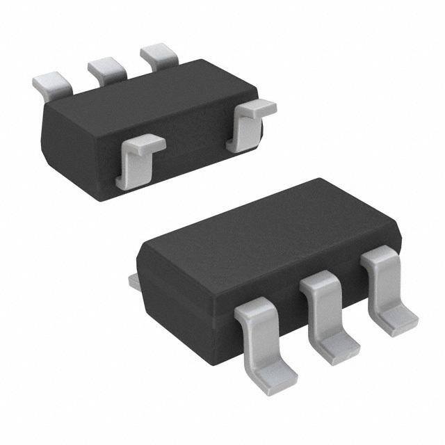
| 描述 | IC REG LDO 1.8V 80MA SOT23-5低压差稳压器 80mA Tiny Adj LDO |
| 产品分类 | |
| 品牌 | Microchip Technology |
| 产品手册 | |
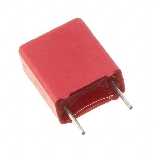
| 产品图片 |
|
| rohs | 符合RoHS无铅 / 符合限制有害物质指令(RoHS)规范要求 |
| 产品系列 | 电源管理 IC,低压差稳压器,Microchip Technology TC1016-1.8VCTTR- |
| 数据手册 | http://www.microchip.com/mymicrochip/filehandler.aspx?ddocname=en026002http://www.microchip.com/mymicrochip/filehandler.aspx?ddocname=en011321点击此处下载产品Datasheethttp://www.microchip.com/mymicrochip/filehandler.aspx?ddocname=en023833 |
| 产品型号 | TC1016-1.8VCTTR |
| 产品目录页面 | |
| 产品种类 | 低压差稳压器 |
| 供应商器件封装 | SOT-23-5 |
| 其它名称 | TC1016-1.8VCTCT |
| 包装 | 剪切带 (CT) |
| 商标 | Microchip Technology |
| 回动电压—最大值 | 300 mV |
| 安装类型 | 表面贴装 |
| 安装风格 | SMD/SMT |
| 封装 | Reel |
| 封装/外壳 | SC-74A,SOT-753 |
| 封装/箱体 | SOT-23-5 |
| 工作温度 | -40°C ~ 125°C |
| 工厂包装数量 | 3000 |
| 最大工作温度 | + 125 C |
| 最大输入电压 | 6 V |
| 最小工作温度 | - 40 C |
| 最小输入电压 | + 2.7 V |
| 标准包装 | 1 |
| 电压-跌落(典型值) | 0.15V @ 80mA |
| 电压-输入 | 2.7 V ~ 6 V |
| 电压-输出 | 1.8V |
| 电压调节准确度 | 0.5 % |
| 电流-输出 | 80mA |
| 电流-限制(最小值) | - |
| 稳压器拓扑 | 正,固定式 |
| 稳压器数 | 1 |
| 线路调整率 | 0.01 % |
| 负载调节 | 0.23 % |
| 输入偏压电流—最大 | 0.053 mA |
| 输出电压 | 1.8 V |
| 输出电流 | 80 mA |
| 输出端数量 | 1 Output |
| 输出类型 | Fixed |


- 商务部:美国ITC正式对集成电路等产品启动337调查
- 曝三星4nm工艺存在良率问题 高通将骁龙8 Gen1或转产台积电
- 太阳诱电将投资9.5亿元在常州建新厂生产MLCC 预计2023年完工
- 英特尔发布欧洲新工厂建设计划 深化IDM 2.0 战略
- 台积电先进制程称霸业界 有大客户加持明年业绩稳了
- 达到5530亿美元!SIA预计今年全球半导体销售额将创下新高
- 英特尔拟将自动驾驶子公司Mobileye上市 估值或超500亿美元
- 三星加码芯片和SET,合并消费电子和移动部门,撤换高东真等 CEO
- 三星电子宣布重大人事变动 还合并消费电子和移动部门
- 海关总署:前11个月进口集成电路产品价值2.52万亿元 增长14.8%


PDF Datasheet 数据手册内容提取
TC1016 80 mA, Tiny CMOS LDO With Shutdown Features General Description • Space-Saving 5-Pin SC-70 and SOT-23 The TC1016 is a high-accuracy (typically ±0.5%), Packages CMOS upgrade for bipolar low dropout regulators (cid:129) Extremely Low Operating Current for Longer (LDOs). The TC1016 is offered in both the SC-70 and Battery Life: 53µA (typ.) SOT-23 packages. The SC-70 package represents a 50% footprint reduction versus the popular SOT-23 (cid:129) Very Low Dropout Voltage package. (cid:129) Rated 80mA Output Current Developed specifically for battery-powered systems, (cid:129) Requires only 1µF Ceramic Output Capacitance the device’s CMOS construction consumes only 53µA (cid:129) High Output Voltage Accuracy: ±0.5% (typ.) typical supply current over the entire 80mA operating (cid:129) 10µsec (typ.) Wake-Up Time from SHDN load range. This can be as much as 60 times less than (cid:129) Power-Saving Shutdown Mode: 0.05µA(typ.) the quiescent operating current consumed by bipolar (cid:129) Overcurrent and Overtemperature Protection LDOs. (cid:129) Pin Compatible Upgrade for Bipolar Regulators With small-space requirements and cost in mind, the TC1016 was developed to be stable over the entire Applications input voltage and output current operating range using low value (1µF ceramic), low Equivalent Series (cid:129) Cellular/GSM/PHS Phones Resistance (ESR) output capacitors. Additional (cid:129) Battery-operated Systems integrated features (such as shutdown, overcurrent (cid:129) Portable Computers and overtemperature protection) further reduce board (cid:129) Medical Instruments space and cost of the entire voltage-regulating application. (cid:129) Electronic Games (cid:129) Pagers Key performance parameters for the TC1016 are low drop out voltage (150mV (typ.) at 80mA output current), low supply current while shutdown (0.05µA typical) and fast stable response to sudden input voltage and load changes. Pin Configurations SC-70 SOT-23 VIN VOUT VOUT NC 5 4 5 4 TC1016 TC1016 1 2 3 1 2 3 SHDN NC GND VIN GND SHDN © 2005 Microchip Technology Inc. DS21666B-page 1
TC1016 1.0 ELECTRICAL *Notice: Static-sensitive device. Unused devices must be stored in conductive material. Protect devices from static dis- CHARACTERISTICS charge and static fields. Stresses above those listed under Absolute Maximum Ratings may cause permanent damage to ABSOLUTE MAXIMUM RATINGS* the device. These are stress ratings only and functional oper- ation of the device at these or any other conditions above Input Voltage.........................................................6.5V those indicated in the operational sections of the Power Dissipation................Internally Limited (Note 7) specifications is not implied. Exposure to Absolute Maximum Operating Temperature.................-40°C < TJ < 125°C Rating Conditions for extended periods may affect device Storage Temperature......................... -65°C to +150°C reliability Maximum Voltage On Any Pin........V + 0.3V to -0.3V IN ELECTRICAL CHARACTERISTICS V = V + 1V, I = 100µA, C = 1.0µF, SHDN > V , T = 25°C, unless otherwise noted. Boldface type specifications apply for IN R L L IH A junction temperatures of – 40°C to +125°C. Parameter Sym Min Typ Max Units Test Conditions Input Operating Voltage V 2.7 — 6.0 V Note1 IN Maximum Output Current I 80 — — mA OUTMAX Output Voltage V V – 2.5% V ±0.5% V + 2.5% V Note2 OUT R R R V Temperature Coefficient TCV — 40 — ppm/°C Note3 OUT OUT Line Regulation (ΔV /ΔV )/V — 0.01 0.2 %/V (V + 1V) < V < 6V OUT IN R R IN Load Regulation (Note4) ΔV /V — 0.23 1 % I = 0.1mA to I OUT R L OUTMAX Dropout Voltage (Note5) V – V — 2 — mV I = 100µA IN OUT L — 100 200 I = 50mA L — 150 300 I = 80mA L Supply Current I — 53 90 µA SHDN = V , I = 0 IN IH L Shutdown Supply Current I — 0.05 0.5 µA SHDN = 0V INSD Power Supply Rejection Ratio PSRR — 58 — dB f =1kHz, I = 50mA L Wake-Up Time t — 10 — µs V = 5V, I = 60mA, WK IN L (from Shutdown mode) C = 1µF, C = 1µF, IN OUT f = 100Hz Settling Time t — 32 — µs V = 5V, I = 60mA,C = S IN L IN (from Shutdown Mode) 1µF, C = 1µF, f = OUT 100Hz Output Short Circuit Current I — 120 — mA V = 0V OUTSC OUT Thermal Regulation V /P — 0.04 — V/W Notes6, 7 OUT D Thermal Shutdown Die T — 160 — °C SD Temperature Thermal Shutdown Hysteresis ΔT — 10 — °C SD Output Noise eN — 800 — nV/√Hz f = 10kHz SHDN Input High Threshold V 60 — — %V V = 2.7V to 6.0V IH IN IN SHDN Input Low Threshold V — — 15 %V V = 2.7V to 6.0V IL IN IN Note 1: The minimum V has to meet two conditions: V ≥ 2.7V and V ≥ (V + 2.5%)+V . IN IN IN R DROPOUT 2: V is the regulator voltage setting. For example: V = 1.8V, 2.7V, 2.8V, 3.0V. R R (V –V )×106 3: TCV = -------O-----U----T----M------A----X-------------O-----U-----T----M-----I---N--------------------- OUT V ×ΔT OUT 4: Regulation is measured at a constant junction temperature using low duty cycle pulse testing. Load regulation is tested over a load range from 0.1mA to the maximum specified output current. Changes in output voltage due to heating effects are covered by the Thermal Regulation specification. 5: Dropout voltage is defined as the input-to-output differential at which the output voltage drops 2% below its nominal value at a 1V differential. 6: Thermal regulation is defined as the change in output voltage at a time T after a change in power dissipation is applied, excluding load or line regulation effects. Specifications are for a current pulse equal to Ilmax at V = 6V for t = 10msec. IN 7: The maximum allowable power dissipation is a function of ambient temperature, the maximum allowable juction temperature and the thermal resistance from junction-to-air (i.e. T, T, θ ). Exceeding the maximum allowable power dissipation causes the device to initiate A J JA thermal shutdown. Please see Section5.0 “Thermal Considerations” of this data sheet for more details. DS21666B-page 2 © 2005 Microchip Technology Inc.
TC1016 2.0 TYPICAL PERFORMANCE CURVES Note: The graphs and tables provided following this note are a statistical summary based on a limited number of samples and are provided for informational purposes only. The performance characteristics listed herein are not tested or guaranteed. In some graphs or tables, the data presented may be outside the specified operating range (e.g., outside specified power supply range) and therefore outside the warranted range. 0.25 0.25 VOUT = 2.7V VOUT = 2.7V 0.2 Dropout Voltage (V) 00.0.01.515 -40°C+25°C+125°C Dropout Voltage (V) 000...112050 IILLOOAADD == 8500 mmAA 0 0.05 0 10 20 30 40 50 60 70 80 -45 -20 5 30 55 80 105 130 Load Current (mA) Temperature(°C) FIGURE 2-1: Dropout Voltage vs. Output FIGURE 2-4: Dropout Voltage vs. Current. Temperature. 0.35 0.18 ation (%) 00..2350 VFuOUll TL =o a2d.7 =V 0 – 80 mA VVININ = = 3 3.3.7VV Current (A) 0000...111.1246 VOUT = 2.7V egul 0.20 VIN = 6.0V cuit 0.08 Load R 0.15 hort Cir 00..0046 0.10 S 0.02 0.05 0 -45 -20 5 30 55 80 105 130 1 2 3 4 5 6 Temperature (°C) Input Voltage FIGURE 2-2: Load Regulation vs. FIGURE 2-5: Short Circuit Current vs. Temperature. Input Voltage. 57.0 57.0 56.0 VOUT = 2.7V 56.0 VIN = 6V VOUT = 2.7V +125°C 55.0 55.0 µA) 54.0 µA) 54.0 urrent ( 5523..00 +25°C urrent ( 5523..00 VIN = 3.3V C C ply 51.0 ply 51.0 Sup 50.0 -40°C Sup 50.0 49.0 49.0 48.0 48.0 47.0 47.0 3.3 3.6 3.9 4.2 4.5 4.8 5.1 5.4 5.7 6.0 -45 -20 5 30 55 80 105 130 Input Voltage (V) Temperature(°C) FIGURE 2-3: Supply Current vs. Input FIGURE 2-6: Supply Current vs. Voltage. Temperature. © 2005 Microchip Technology Inc. DS21666B-page 3
TC1016 0.25 0.20 VOUT = 3.0V 0.18 VOUT = 3.0V 0.2 0.16 ILOAD = 80 mA Dropout Voltage (V) 00.1.15 +1+22-554°°0CC°C Dropout Voltage (V) 000000......000111468024 ILOAD = 50 mA 0.05 0.02 0.00 0 -45 -20 5 30 55 80 105 130 0 10 20 30 40 50 60 70 80 Load Current (mA) Temperature (°C) FIGURE 2-7: Dropout Voltage vs. Output FIGURE 2-10: Dropout Voltage vs. Current. Temperature. 0.30 54.0 VOUT = 3.0V VOUT = 3.0V Full Load = 0 – 80 mA 0.25 53.0 %) VIN = 6.0V A) 52.0 +125°C ulation ( 00..1250 VIN = 3.3V VIN = 4.0V urrent (µ 51.0 +25°C Load Reg 0.10 Supply C 4590..00 -40°C 0.05 48.0 0.00 47.0 -45 -20 5 30 55 80 105 130 3.3 3.6 3.9 4.2 4.5 4.8 5.1 5.4 5.7 6.0 Temperature (°C) Input Voltage (V) FIGURE 2-8: Load Regulation vs. FIGURE 2-11: Supply Current vs. Input Temperature. Voltage 54.0 2.797 53.0 VOUT = 3.0V VIN = 6.0V 2.796 +25°C +125°C VOUT = 2.8V ent (µA) 5512..00 VIN = 3.3V age (V) 22..779945 ply Curr 50.0 put Volt 22..779923 Sup 49.0 Out 2.791 -40°C 48.0 2.790 47.0 2.789 -45 -20 5 30 55 80 105 130 3.3 3.6 3.9 4.2 4.5 4.8 5.1 5.4 5.7 6 Temperature (°C) Input Voltage (V) FIGURE 2-9: Supply Current vs. FIGURE 2-12: Output Voltage vs. Supply Temperature. Voltage. DS21666B-page 4 © 2005 Microchip Technology Inc.
TC1016 2.797 2.798 2.796 VIN = 3.3V VOUT = 2.8V 2.797 VOUT = 2.8V 2.795 2.796 VIN = 3.3V V) 2.794 V) e ( e ( 2.795 g 2.793 g ut Volta 22..779912 VIN = 6.0V ut Volta 22..779934 VIN = 6.0V utp 2.790 utp 2.792 VIN = 4.0V O O 2.789 2.791 2.788 2.790 2.787 2.789 0 10 20 30 40 50 60 70 80 -45 -20 5 30 55 80 105 130 Output Current (mA) Temperature (°C) FIGURE 2-13: Output Voltage vs. Output FIGURE 2-16: Output Voltage vs. Current. Temperature. 0.250 100 VIN = 4.0V VOUT = 3.0V nt (µA) 0.200 +125°C Hz) 10 CCIOIOUNUT = T= =1 4 10μ FμmFA down Curre 00..110500 √Noise (µV/ 1 hut 0.1 S 0.050 +25°C 0.000 0.01 2.7 3.0 3.3 3.6 3.9 4.2 4.5 4.8 5.1 5.4 5.7 6.0 10 100 1000 10000 100000 1000000 Input Voltage (V) Frequency (Hz) FIGURE 2-14: Shutdown Current vs. Input FIGURE 2-17: Output Noise vs. Frequency. Voltage. -100 1.E+01VVIINNDACC == 120.80V mVp-p 1.E+03 ICOOUUT T= = 1 10 0μ Fμ1.E+05 AX7R Ceramic -100 10VVIINNDACC == 120.80V mVp-p 1000 ICOOUUT T= = 1 1 m μA1F00000 X7R Ceramic VOUTDC = 1.8V VOUTDC = 1.8V -20 -20 PSRR(dB) ---543000 PSRR(dB) ---543000 -60 -60 -70 -70 -80 -80 10 100 1K 10K 100K 1M 10 100 1K 10K 100K 1M Frequency (Hz) Frequency (Hz) FIGURE 2-15: Power Supply Rejection FIGURE 2-18: Power Supply Rejection Ratio vs. Frequency. Ratio vs. Frequency. © 2005 Microchip Technology Inc. DS21666B-page 5
TC1016 -100 10VVVIIONNUDATCCD ==C =12 0.180.V8 mVVp-p 1000 ICOOUUT T= = 5 10 μm100F000A X7R Ceramic VCCIIONNU ==T 21=.0 81 Vµ µFF Ceramic -20 B)-30 VOUT = 1.8V d R(-40 R S P-50 IOUT = 0.1 mA to 60 mA -60 -70 -80 10 100 1K 10K 100K 1M Frequency (Hz) FIGURE 2-19: Power Supply Rejection FIGURE 2-22: Load Transient Response. Ratio vs. Frequency. VCCIIONNU ==T 21=.0 81 Vµ µFF Ceramic VOUT = 1.8V VCCIIONNU ==T 21=.0 81 Vµ µFF Ceramic VOUT = 1.8V IOUT = 0.1 mA to 60 mA Shutdown Input FIGURE 2-20: Wake-Up Response. FIGURE 2-23: Load Transient Response. VCCIIONNU ==T 21=.0 84 Vµ.7F µF Ceramic VOUT = 1.8V ICCLOIONAU =DT 0== µ16F 0µ Fm ACeramic VOUT = 1.8V IOUT = 2.8V to 3.8V Shutdown Input FIGURE 2-21: Wake-Up Response. FIGURE 2-24: Line Transient Response. DS21666B-page 6 © 2005 Microchip Technology Inc.
TC1016 ILOAD = 60 mA CIN = 0 µF COUT = 4.7 µF Ceramic VOUT = 1.8V VOUT = 2.8V to 3.8V FIGURE 2-25: Line Transient Response. ILOAD = 100 µA CIN = 0 µF COUT = 1 µF Ceramic VIN = 4V to 5V VOUT = 2.8V FIGURE 2-26: Line Transient Response. ILOAD = 100 µA CIN = 0 µF COUT = 10 µF Ceramic VIN = 4V to 5V VOUT = 2.8V FIGURE 2-27: Line Transient Response. © 2005 Microchip Technology Inc. DS21666B-page 7
TC1016 3.0 PIN DESCRIPTIONS The descriptions of the pins are listed in Table 3-1. TABLE 3-1: PIN FUNCTION TABLE 5-Pin Pin No. Name Function SC-70 5-Pin SOT-23 1 3 SHDN Shutdown control input 2 4 NC No connect 3 2 GND Ground terminal 4 5 V Regulated voltage output OUT 5 1 V Unregulated supply input IN 3.1 Shutdown Control Input (SHDN) 3.4 Unregulated Supply Input (V ) IN The regulator is fully enabled when a logic-high is The minimum V has to meet two conditions in order IN applied to SHDN. The regulator enters shutdown when to ensure that the output maintains regulation: a logic-low is applied to this input. During shutdown, the V ≥2.7V and V ≥ [(V + 2.5%) + V ]. The IN IN R DROPOUT output voltage falls to zero and the supply current is maximum V should be less than or equal to 6V. IN reduced to 0.05µA (typ.) Power dissipation may limit V to a lower potential in IN order to maintain a junction temperature below 125°C. 3.2 Ground Terminal (GND) Refer to Section5.0 “Thermal Considerations”, for determining junction temperature. For best performance, it is recommended that the It is recommended that V be bypassed to GND with a ground pin be tied to a ground plane. IN ceramic capacitor. 3.3 Regulated Voltage Output (V ) OUT Bypass the regulated voltage output to GND with a minimum capacitance of 1µF. A ceramic bypass capacitor is recommended for best performance. DS21666B-page 8 © 2005 Microchip Technology Inc.
TC1016 4.0 DETAILED DESCRIPTION MOSFET is turned on. If the internal power dissipation is still high enough for the junction to rise to 160°C, it The TC1016 is a precision, fixed-output, linear voltage will again shut off and cool. The maximum operating regulator. The internal linear pass element is a P- junction temperature of the device is 125°C. Steady- channel MOSFET. As with all P-channel CMOS LDOs, state operation at or near the 160°C overtemperature there is a body drain diode, with the cathode connected point can lead to permanent damage of the device. to V and the anode connected to V (Figure4-1). IN OUT The output voltage (V ) remains stable over the OUT As shown in Figure4-1, the output voltage of the LDO entire input operating voltage range (2.7V to 6.0V), as is sensed and divided down internally to reduce well as the entire load range (0mA to 80mA). The external component count. The internal error amplifier output voltage is sensed through an internal resistor has a fixed, band gap reference on the inverting input, divider and compared with a precision internal voltage with the sensed output voltage on the non-inverting reference. Several fixed-output voltages are available input. The error amplifier output will pull the gate by changing the value of the internal resistor divider. voltage down until the inputs of the error amplifier are Figure4-2 shows a typical application circuit. The reg- equal in order to regulate the output voltage. ulator is enabled anytime the shutdown input pin is at By sensing the current in the P-channel MOSFET, the or above V , and shutdown (disabled) anytime the IH maximum current delivered to the load is limited to a shutdown input pin is below V . For applications where IL typical value of 120mA, preventing excessive current the SHDN feature is not used, tie the SHDN pin directly from damaging the Printed Circuit Board (PCB) in the to the input supply voltage source. While in shutdown, event of a shorted or faulted load. the supply current decreases to 0.05µA (typ.) and the An internal thermal sensing device is used to monitor P-channel MOSFET is turned off. the junction temperature of the LDO. When the sensed As shown in Figure4-2, batteries have internal source temperature is over the set threshold of 160°C (typ.), impedance. An input capacitor in used to lower the the P-channel MOSFET is turned off. When the input impedance of the LDO. In some applications, high MOSFET is off, the power dissipation internal to the input impedance can cause the LDO to become device is almost zero. The device cools until the unstable. Adding more input capacitance can junction temperature is approximately 150°C and the compensate for this. 1 SHDN VIN 5 Current Limit 2 NC V IN SHDN V - Body ControlREF +EA Diode Error Amp 3 GND VOUT 4 TOevmepr. R1 R2 Feedback Resistors FIGURE 4-1: TC1016 Block Diagram. 1 SHDN VIN 5 R TC1016 CIN 1µF Ceramic SOURCE RY 2 NC E T T A 3 4 B GND VOUT Load COUT 1µF Ceramic FIGURE 4-2: Typical Application Circuit. © 2005 Microchip Technology Inc. DS21666B-page 9
TC1016 4.1 Input Capacitor 4.3 Turn-On Response Low input source impedance is necessary for the LDO The turn on response is defined as two separate to operate properly. When operating from batteries, or response categories, Wake-up Time (t ) and Settling WK in applications with long lead length (> 10") between Time (t ). S the input source and the LDO, some input capacitance The TC1016 has a fast t (10µsec, typ.) when WK is required. A minimum of 0.1µF is recommended for released from shutdown. Figure4-3 provides the most applications and the capacitor should be placed TC1016’s t . The t is defined as the time it takes WK WK as close to the input of the LDO as is practical. Larger for the output to rise to 2% of the V value after being OUT input capacitors will help reduce the input impedance released from shutdown. and further reduce any high-frequency noise on the The total turn-on response is defined as the t (see input and output of the LDO. S Figure4-3). The t (inclusive with t ) is defined as the S WK condition when the output is within 98% of its fully 4.2 Output Capacitor enabled value (42µsec, typ.) when released from shut- A minimum output capacitance of 1µF for the TC1016 down. The settling time of the output voltage is is required for stability. The ESR requirements on the dependent on load conditions and output capacitance output capacitor are between 0 and 2 ohms. The output on VOUT (RC response). capacitor should be located as close to the LDO output Table4-1 demonstrates the typical turn-on response as is practical. Ceramic materials X7R and X5R have timing for different input voltage power-up frequencies: low temperature coefficients and are well within the V = 2.8V, V = 5.0V, I = 60mA and C = 1µF. OUT IN OUT OUT acceptable ESR range required. A typical 1µF X5R 0805 capacitor has an ESR of 50milli-ohms. Larger TABLE 4-1: TYPICAL TURN-ON output capacitors can be used with the TC1016 to RESPONSE TIMING improve dynamic behavior and input ripple rejection performance. Frequency Typical (t ) Typical (t ) WK S Ceramic, aluminum electrolytic or tantalum capacitor 1000Hz 5.3µsec 14µsec types can be used. Since many aluminum electrolytic 500Hz 5.9µsec 16µsec capacitors freeze at approximately –30°C, ceramic or 100Hz 9.8µsec 32µsec solid tantalums are recommended for applications operating below –25°C. When operating from sources 50Hz 14.5µsec 52µsec other than batteries, supply noise rejection and tran- 10Hz 17.2µsec 77µsec sient response can be improved by increasing the value of the input and output capacitors, and by employing passive filtering techniques. V IH SHDN VIL tS 98% V 2% OUT t WK FIGURE 4-3: Wake-Up Time from Shutdown. DS21666B-page 10 © 2005 Microchip Technology Inc.
TC1016 5.0 THERMAL CONSIDERATIONS Given the following example: V = 3.0V to 4.1V IN 5.1 Thermal Shutdown V = 2.8V ±2.5% OUT Integrated thermal-protection circuitry shuts the I = 60mA (output current) LOAD regulator off when die temperature exceeds T = 55°C (max. ambient temp.) AMAX approximately 160°C. The regulator remains off until Find: the die temperature drops to approximately 150°C. 1. Internal power dissipation: 5.2 Power Dissipation P = (V –V )×I DMAX IN_MAX OUT_MIN LOAD The TC1016 is available in the SC-70 package. The = (4.1V–2.8×(0.975))×60mA thermal resistance for the SC-70 package is approxi- = 82.2mW mately 450°C/W when the copper area used in the PCB layout is similar to the JEDECJ51-7 high thermal 2. Junction temperature: conductivity or Semi G42-88 standards. For applica- T = P ×Rθ tions with larger or thicker copper areas, the thermal J_MAX DMAX JA resistance can be lowered. See AN792 “A Method to = 82.2mWatts×450°C/W+T AMAX Determine How Much Power a SOT23 Can Dissipate in = 37°C+55°C an Application” (DS00792), for a method to determine = 92°C the thermal resistance for a particular application. 3. Maximum allowable dissipation: The TC1016 power dissipation capability is dependant upon several variables: input voltage, output voltage, T –T P = ----J--_--M----A----X-------------A---_--M-----A---X-- load current, ambient temperature and maximum D Rθ JA junction temperature. The absolute maximum steady- 125°C–55°C state junction temperature is rated at 125°C. The power = ------4---5---0----°--C-----/-W----------- dissipation within the device is equal to: = 155mW EQUATION 5-1: In this example, the TC1016 dissipates approximately 82.2mW and the junction temperature is raised 37°C P = (V –V )×I +V ×I D IN OUT LOAD IN GND over the 55°C ambient to 92°C. The absolute maximum power dissipation is 155mW when given a maximum The VIN x IGND term is typically very small when com- ambient temperature of 55°C. pared to the (V -V ) x I term simplifying the IN OUT LOAD Input voltage, output voltage or load current limits can power dissipation within the LDO to be: also be determined by substituting known values in Equation5-2 and Equation5-3. EQUATION 5-2: 5.3 Layout Considerations P = (V –V )×I D IN OUT LOAD The primary path for heat conduction out of the SC-70 To determine the maximum power dissipation package is through the package leads. Using heavy, capability, the following equation is used: wide traces at the pads of the device will facilitate the removal of heat within the package, thus lowering the EQUATION 5-3: thermal resistance Rθ . By lowering the thermal JA resistance, the maximum internal power dissipation (T –T ) P = -------J-_---M----A---X-------------A---_---M----A---X----- capability of the package is increased. DMAX Rθ JA Where: SHDN T = maximum junction temperature allowed J_MAX V U1 V IN OUT T =themaximumambienttemperatureallowed A_MAX Rθ = the thermal resistance from junction-to-air JA C C 1 2 GND FIGURE 5-1: Suggested layout © 2005 Microchip Technology Inc. DS21666B-page 11
TC1016 6.0 PACKAGE INFORMATION 6.1 Package Marking Information 5-Lead SC-70 Example: Part Number Code XXN (Front) TC1016 – 1.8VLT AE AE7 (Front) YWW (Back) TC1016 – 1.85VLT AW 432 (Back) TC1016 – 2.6VLT AF TC1016 – 2.7VLT AG TC1016 – 2.8VLT AH 5-Lead SC-70 TC1016 – 2.85VLT AJ Example: TC1016 – 2.9VLT AK TC1016 – 3.0VLT AL XXNN TC1016 – 3.3VLT AM AE74 TC1016 – 4.0VLT AP Legend: XX...X Customer-specific information* Y Year code (last digit of calendar year) YY Year code (last 2 digits of calendar year) WW Week code (week of January 1 is week ‘01’) NNN Alphanumeric traceability code e3 Pb-free JEDEC designator for Matte Tin (Sn) * This package is Pb-free. The Pb-free JEDEC designator ( e 3 ) can be found on the outer packaging for this package. Note: In the event the full Microchip part number cannot be marked on one line, it will be carried over to the next line, thus limiting the number of available characters for customer-specific information. DS21666B-page 12 © 2005 Microchip Technology Inc.
TC1016 6.1 Package Marking Information (Continued) Part Number Code TC1016 – 1.8VCT HK TC1016 – 1.85VCT HW 5-Lead SOT-23 Example TC1016 – 2.6VCT HL TC1016 – 2.7VCT HM TC1016 – 2.8VCT HP XXNN HK73 TC1016 – 2.85VCT HQ TC1016 – 2.9VCT HR TC1016 – 3.0VCT HS TC1016 – 3.3VCT HT TC1016 – 4.0VCT HU © 2005 Microchip Technology Inc. DS21666B-page 13
TC1016 5-Lead Plastic Small Outline Transistor (LT) (SC-70) E E1 D p B n 1 Q1 A2 A c A1 L Units INCHES MILLIMETERS* Dimension Limits MIN NOM MAX MIN NOM MAX Number of Pins n 5 5 Pitch p .026 (BSC) 0.65 (BSC) Overall Height A .031 .043 0.80 1.10 Molded Package Thickness A2 .031 .039 0.80 1.00 Standoff A1 .000 .004 0.00 0.10 Overall Width E .071 .094 1.80 2.40 Molded Package Width E1 .045 .053 1.15 1.35 Overall Length D .071 .087 1.80 2.20 Foot Length L .004 .012 0.10 0.30 Top of Molded Pkg to Lead Shoulder Q1 .004 .016 0.10 0.40 Lead Thickness c .004 .007 0.10 0.18 Lead Width B .006 .012 0.15 0.30 *Controlling Parameter Notes: Dimensions D and E1 do not include mold flash or protrusions. Mold flash or protrusions shall not exceed .005" (0.127mm) per side. JEITA (EIAJ) Standard: SC-70 Drawing No. C04-061 Dimensions: inches (mm) DS21666B-page 14 © 2005 Microchip Technology Inc.
TC1016 5-Lead Plastic Small Outline Transistor (OT) (SOT-23) E E1 p B p1 D n 1 α c A A2 φ A1 L β Units INCHES* MILLIMETERS Dimension Limits MIN NOM MAX MIN NOM MAX Number of Pins n 5 5 Pitch p .038 0.95 Outside lead pitch (basic) p1 .075 1.90 Overall Height A .035 .046 .057 0.90 1.18 1.45 Molded Package Thickness A2 .035 .043 .051 0.90 1.10 1.30 Standoff A1 .000 .003 .006 0.00 0.08 0.15 Overall Width E .102 .110 .118 2.60 2.80 3.00 Molded Package Width E1 .059 .064 .069 1.50 1.63 1.75 Overall Length D .110 .116 .122 2.80 2.95 3.10 Foot Length L .014 .018 .022 0.35 0.45 0.55 Foot Angle φ 0 5 10 0 5 10 Lead Thickness c .004 .006 .008 0.09 0.15 0.20 Lead Width B .014 .017 .020 0.35 0.43 0.50 Mold Draft Angle Top α 0 5 10 0 5 10 Mold Draft Angle Bottom β 0 5 10 0 5 10 *Controlling Parameter Notes: Dimensions D and E1 do not include mold flash or protrusions. Mold flash or protrusions shall not exceed .005" (0.127mm) per side. EIAJ Equivalent: SC-74A Drawing No. C04-091 © 2005 Microchip Technology Inc. DS21666B-page 15
TC1016 NOTES: DS21666B-page 16 © 2005 Microchip Technology Inc.
TC1016 APPENDIX A: REVISION HISTORY Revision B (March 2005) (cid:129) Updated Section6.0 “Package Information” to include old and new packaging examples, as well as replaced SC-70 package diagram with up-to- date version. Added additional voltage options (cid:129) Added SOT-23 package and voltage options. (cid:129) Applied new template and rearranged sections to be consistent with current documentation. .Revision A (October 2001) (cid:129) Original Release of this Document. © 2005 Microchip Technology Inc. DS21666B-page 17
TC1016 NOTES: DS21666B-page 18 © 2005 Microchip Technology Inc.
TC1016 PRODUCT IDENTIFICATION SYSTEM To order or obtain information, e.g., on pricing or delivery, refer to the factory or the listed sales office. PART NO. X.XX X XXXX Examples: Device Voltage Temperature Package a) TC1016-1.8VCTTR: 80mA Tiny CMOS Options Range LDO with Shutdown, SOT-23 Package. a) TC1016-1.8VLTTR: 80mA Tiny CMOS LDO Device: TC1016: 80mA Tiny CMOS LDO with Shutdown with Shutdown, SC-70 Package. Voltage Options*: 1.8V b) TC1016-1.85VCTTR: 80mA Tiny CMOS (Standard) LDO with Shutdown, 1.85V SOT-23 Package. 2.6V 2.7V c) TC1016-1.85VLTTR: 80mA Tiny CMOS LDO 2.8V with Shutdown, 2.85V SC-70 Package. 2.9V d) TC1016-2.6VCTTR: 80mA Tiny CMOS 3.0V LDO with Shutdown, 3.3V SOT-23 Package. 4.0V e) TC1016-2.6VLTTR: 80mA Tiny CMOS LDO * Other voltage options available. Please contact your local with Shutdown, Microchip sales office for details. SC-70 Package. Temperature Range: V = -40°C to +125°C f) TC1016-2.7VCTTR: 80mA Tiny CMOS LDO with Shutdown, SOT-23 Package. Packages: LTTR = 5-pin SC-70 (Tape and Reel) g) TC1016-2.7VLTTR: 80mA Tiny CMOS LDO with Shutdown, CTTR = 5-pin SOT-23 (Tape and Reel) SC-70 Package. h) TC1016-2.8VCTTR: 80mA Tiny CMOS LDO with Shutdown, SOT-23 Package. i) TC1016-2.8VLTTR: 80mA Tiny CMOS LDO with Shutdown, SC-70 Package. j) TC1016-2.85VLTTR: 80mA Tiny CMOS LDO with Shutdown, SC-70 Package. © 2005 Microchip Technology Inc. DS21666A-page19
TC1016 NOTES: DS21666A-page20 © 2005 Microchip Technology Inc.
Note the following details of the code protection feature on Microchip devices: (cid:129) Microchip products meet the specification contained in their particular Microchip Data Sheet. (cid:129) Microchip believes that its family of products is one of the most secure families of its kind on the market today, when used in the intended manner and under normal conditions. (cid:129) There are dishonest and possibly illegal methods used to breach the code protection feature. All of these methods, to our knowledge, require using the Microchip products in a manner outside the operating specifications contained in Microchip’s Data Sheets. Most likely, the person doing so is engaged in theft of intellectual property. (cid:129) Microchip is willing to work with the customer who is concerned about the integrity of their code. (cid:129) Neither Microchip nor any other semiconductor manufacturer can guarantee the security of their code. Code protection does not mean that we are guaranteeing the product as “unbreakable.” Code protection is constantly evolving. We at Microchip are committed to continuously improving the code protection features of our products. Attempts to break Microchip’s code protection feature may be a violation of the Digital Millennium Copyright Act. If such acts allow unauthorized access to your software or other copyrighted work, you may have a right to sue for relief under that Act. Information contained in this publication regarding device Trademarks applications and the like is provided only for your convenience The Microchip name and logo, the Microchip logo, Accuron, and may be superseded by updates. It is your responsibility to dsPIC, KEELOQ, microID, MPLAB, PIC, PICmicro, PICSTART, ensure that your application meets with your specifications. PROMATE, PowerSmart, rfPIC, and SmartShunt are MICROCHIP MAKES NO REPRESENTATIONS OR WAR- registered trademarks of Microchip Technology Incorporated RANTIES OF ANY KIND WHETHER EXPRESS OR IMPLIED, in the U.S.A. and other countries. WRITTEN OR ORAL, STATUTORY OR OTHERWISE, RELATED TO THE INFORMATION, INCLUDING BUT NOT AmpLab, FilterLab, Migratable Memory, MXDEV, MXLAB, LIMITED TO ITS CONDITION, QUALITY, PERFORMANCE, PICMASTER, SEEVAL, SmartSensor and The Embedded MERCHANTABILITY OR FITNESS FOR PURPOSE. Control Solutions Company are registered trademarks of Microchip disclaims all liability arising from this information and Microchip Technology Incorporated in the U.S.A. its use. Use of Microchip’s products as critical components in Analog-for-the-Digital Age, Application Maestro, dsPICDEM, life support systems is not authorized except with express dsPICDEM.net, dsPICworks, ECAN, ECONOMONITOR, written approval by Microchip. No licenses are conveyed, FanSense, FlexROM, fuzzyLAB, In-Circuit Serial implicitly or otherwise, under any Microchip intellectual property Programming, ICSP, ICEPIC, MPASM, MPLIB, MPLINK, rights. MPSIM, PICkit, PICDEM, PICDEM.net, PICLAB, PICtail, PowerCal, PowerInfo, PowerMate, PowerTool, rfLAB, rfPICDEM, Select Mode, Smart Serial, SmartTel, Total Endurance and WiperLock are trademarks of Microchip Technology Incorporated in the U.S.A. and other countries. SQTP is a service mark of Microchip Technology Incorporated in the U.S.A. All other trademarks mentioned herein are property of their respective companies. © 2005, Microchip Technology Incorporated, Printed in the U.S.A., All Rights Reserved. Printed on recycled paper. Microchip received ISO/TS-16949:2002 quality system certification for its worldwide headquarters, design and wafer fabrication facilities in Chandler and Tempe, Arizona and Mountain View, California in October 2003. The Company’s quality system processes and procedures are for its PICmicro® 8-bit MCUs, KEELOQ® code hopping devices, Serial EEPROMs, microperipherals, nonvolatile memory and analog products. In addition, Microchip’s quality system for the design and manufacture of development systems is ISO 9001:2000 certified. © 2005 Microchip Technology Inc. DS21666B-page 21
WORLDWIDE SALES AND SERVICE AMERICAS ASIA/PACIFIC ASIA/PACIFIC EUROPE Corporate Office Australia - Sydney India - Bangalore Austria - Weis 2355 West Chandler Blvd. Tel: 61-2-9868-6733 Tel: 91-80-2229-0061 Tel: 43-7242-2244-399 Chandler, AZ 85224-6199 Fax: 61-2-9868-6755 Fax: 91-80-2229-0062 Fax: 43-7242-2244-393 Tel: 480-792-7200 China - Beijing India - New Delhi Denmark - Ballerup Fax: 480-792-7277 Tel: 86-10-8528-2100 Tel: 91-11-5160-8631 Tel: 45-4450-2828 Technical Support: Fax: 86-10-8528-2104 Fax: 91-11-5160-8632 Fax: 45-4485-2829 http://support.microchip.com Web Address: China - Chengdu Japan - Kanagawa France - Massy www.microchip.com Tel: 86-28-8676-6200 Tel: 81-45-471- 6166 Tel: 33-1-69-53-63-20 Fax: 86-28-8676-6599 Fax: 81-45-471-6122 Fax: 33-1-69-30-90-79 Atlanta Alpharetta, GA China - Fuzhou Korea - Seoul Germany - Ismaning Tel: 770-640-0034 Tel: 86-591-8750-3506 Tel: 82-2-554-7200 Tel: 49-89-627-144-0 Fax: 770-640-0307 Fax: 86-591-8750-3521 Fax: 82-2-558-5932 or Fax: 49-89-627-144-44 China - Hong Kong SAR 82-2-558-5934 Italy - Milan Boston Westborough, MA Tel: 852-2401-1200 Singapore Tel: 39-0331-742611 Tel: 774-760-0087 Fax: 852-2401-3431 Tel: 65-6334-8870 Fax: 39-0331-466781 Fax: 774-760-0088 China - Shanghai Fax: 65-6334-8850 Netherlands - Drunen Chicago Tel: 86-21-5407-5533 Taiwan - Kaohsiung Tel: 31-416-690399 Itasca, IL Fax: 86-21-5407-5066 Tel: 886-7-536-4818 Fax: 31-416-690340 Tel: 630-285-0071 China - Shenyang Fax: 886-7-536-4803 England - Berkshire Fax: 630-285-0075 Tel: 86-24-2334-2829 Taiwan - Taipei Tel: 44-118-921-5869 Dallas Fax: 86-24-2334-2393 Tel: 886-2-2500-6610 Fax: 44-118-921-5820 Addison, TX China - Shenzhen Fax: 886-2-2508-0102 Tel: 972-818-7423 Tel: 86-755-8203-2660 Taiwan - Hsinchu Fax: 972-818-2924 Fax: 86-755-8203-1760 Tel: 886-3-572-9526 Detroit China - Shunde Fax: 886-3-572-6459 Farmington Hills, MI Tel: 86-757-2839-5507 Tel: 248-538-2250 Fax: 86-757-2839-5571 Fax: 248-538-2260 China - Qingdao Kokomo Tel: 86-532-502-7355 Kokomo, IN Fax: 86-532-502-7205 Tel: 765-864-8360 Fax: 765-864-8387 Los Angeles Mission Viejo, CA Tel: 949-462-9523 Fax: 949-462-9608 San Jose Mountain View, CA Tel: 650-215-1444 Fax: 650-961-0286 Toronto Mississauga, Ontario, Canada Tel: 905-673-0699 Fax: 905-673-6509 03/01/05 DS21666B-page 22 © 2005 Microchip Technology Inc.