ICGOO在线商城 > TB1100L-13
 Datasheet下载
- 型号: TB1100L-13
- 制造商: Diodes Inc.
- 库位|库存: xxxx|xxxx
- 要求:
| 数量阶梯 | 香港交货 | 国内含税 |
| +xxxx | $xxxx | ¥xxxx |
查看当月历史价格
查看今年历史价格
TB1100L-13产品简介:
ICGOO电子元器件商城为您提供TB1100L-13由Diodes Inc.设计生产,在icgoo商城现货销售,并且可以通过原厂、代理商等渠道进行代购。 提供TB1100L-13价格参考以及Diodes Inc.TB1100L-13封装/规格参数等产品信息。 你可以下载TB1100L-13参考资料、Datasheet数据手册功能说明书, 资料中有TB1100L-13详细功能的应用电路图电压和使用方法及教程。
| 参数 | 数值 |
| 产品目录 | |
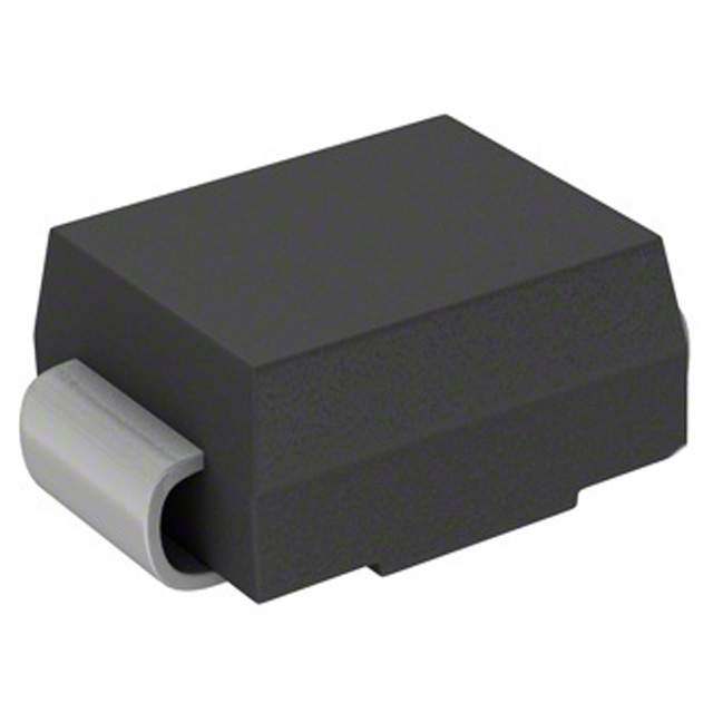
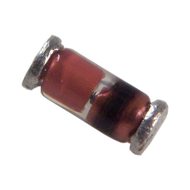
| 描述 | THYRISTOR PROTECT BI-DIR 30A SMBTHYRISTOR PROTECT BI-DIR 30A SMB |
| 产品分类 | |
| 品牌 | Diodes/ZetexDiodes Incorporated |
| 数据手册 | |
| 产品图片 |
|
| 产品型号 | TB1100L-13TB1100L-13 |
| rohs | 含铅 / 不符合限制有害物质指令(RoHS)规范要求含铅 / 不符合限制有害物质指令(RoHS)规范要求 |
| 产品系列 | -- |
| 产品目录页面 | |
| 元件数 | 11 |
| 其它名称 | TB1100LDICT |
| 其它图纸 |
|
| 包装 | 剪切带 (CT)带卷 (TR) |
| 封装/外壳 | DO-214AA,SMBDO-214AA,SMB |
| 标准包装 | 13,000 |
| 电压-导通 | 130V130V |
| 电压-断态 | 90V90V |
| 电压-通态 | 3.5V3.5V |
| 电容 | 60pF60pF |
| 电流-保持(Ih) | 150mA150mA |
| 电流-峰值脉冲(10/1000µs) | 30A30A |
| 电流-峰值脉冲(8/20µs) | 150A150A |


- 商务部:美国ITC正式对集成电路等产品启动337调查
- 曝三星4nm工艺存在良率问题 高通将骁龙8 Gen1或转产台积电
- 太阳诱电将投资9.5亿元在常州建新厂生产MLCC 预计2023年完工
- 英特尔发布欧洲新工厂建设计划 深化IDM 2.0 战略
- 台积电先进制程称霸业界 有大客户加持明年业绩稳了
- 达到5530亿美元!SIA预计今年全球半导体销售额将创下新高
- 英特尔拟将自动驾驶子公司Mobileye上市 估值或超500亿美元
- 三星加码芯片和SET,合并消费电子和移动部门,撤换高东真等 CEO
- 三星电子宣布重大人事变动 还合并消费电子和移动部门
- 海关总署:前11个月进口集成电路产品价值2.52万亿元 增长14.8%

PDF Datasheet 数据手册内容提取
TB0640L - TB3500L 30A BI-DIRECTIONAL SURFACE MOUNT THYRISTOR SURGE PROTECTIVE DEVICE Features UNDER DEVELOPMENT (cid:183) 30A Peak Pulse Current @ 10/1000(cid:109)s T C (cid:183) 150A Peak Pulse Current @ 8/20(cid:109)s U (cid:183) 58 - 320V Stand-Off Voltages D (cid:183) Oxide-Glass Passivated Junction A O (cid:183) Bi-Directional Protection In a Single Device SMB R (cid:183) High Off-State impedance and Low On-State Dim Min Max P Voltage A 4.06 4.57 B C W Mechanical Data B 3.30 3.94 E C 1.96 2.21 N (cid:183) Case: SMB, Molded Plastic D 0.15 0.31 (cid:183) Plastic Material: UL Flammability Classification Rating 94V-0 D E 5.21 5.59 (cid:183) Moisture sensitivity: Level 1 per J-STD-020A F 0.05 0.20 G (cid:183) Terminals: Solder Plated Terminal - G 2.01 2.62 Solderable per MIL-STD-202, Method 208 H F H 0.76 1.52 (cid:183) Polarity: None; Bi-Directional Devices Have No E All Dimensions in mm Polarity Indicator (cid:183) Weight: 0.093 grams (approx.) (cid:183) Marking: Date Code and Marking Code (See Page 4) (cid:183) Ordering Information: See Page 4 Maximum Ratings @ TA = 25(cid:176)C unless otherwise specified Single phase, half wave, 60Hz, resistive or inductive load. For capacitive load, derate current by 20%. Characteristic Symbol Value Unit Non-Repetitive Peak Impulse Current @10/1000us Ipp 30 A Non-Repetitive Peak On-State Current @8.3ms (one-half cycle) ITSM 15 A Junction Temperature Range Tj -40 to +150 (cid:176)C Storage Temperature Range TSTG -55 to +150 (cid:176)C Thermal Resistance, Junction to Lead R(cid:113)JL 30 °C/W Thermal Resistance, Junction to Ambient R(cid:113)JA 120 °C/W Typical Positive Temperature Coefficient for Breakdown Voltage (cid:68)VBR/(cid:68)Tj 0.1 %/°C Maximum Rated Surge Waveform %) Waveform Standard Ipp (A) T ( 100 Peak Value (Ipp) N 2/10 us GR-1089-CORE 200 RE tr = rise time to peak value 8/20 us IEC 61000-4-5 150 CUR tp = decay time to half value 10/160 us FCC Part 68 100 LSE Half Value U P 50 10/700 us ITU-T, K20/K21 60 K A E 1100//1506000 u uss GRFC-1C0 8P9a-Crt O68RE 5300 I, PPP 0 0 tr tp TIME DS30359 Rev. 2 - 1 1 of 4 TB0640L - TB3500L
Electrical Characteristics @ TA = 25(cid:176)C unless otherwise specified T Rated Off-State On-State Breakover C Repetitive Leakage Breakover Holding Current Off-State Voltage Current U Part Number OVfof-lStatgatee CuVrrDeRnMt @ Voltage @ IT = 1A IBO IH Capacitance MCaorkdieng D Min Min O VDRM (V) IDRM (uA) VBO (V) VT (V) (mA) Max (mA) (mA) Max (mA) CO (pF) R TB0640L 58 5 77 3.5 50 800 150 800 100 T064L P TB0720L 65 5 88 3.5 50 800 150 800 100 T072L W TB0900L 75 5 98 3.5 50 800 150 800 100 T090L E TB1100L 90 5 130 3.5 50 800 150 800 60 T110L N TB1300L 120 5 160 3.5 50 800 150 800 60 T130L TB1500L 140 5 180 3.5 50 800 150 800 60 T150L TB1800L 160 5 220 3.5 50 800 150 800 60 T180L TB2300L 190 5 265 3.5 50 800 150 800 40 T230L TB2600L 220 5 300 3.5 50 800 150 800 40 T260L TB3100L 275 5 350 3.5 50 800 150 800 40 T310L TB3500L 320 5 400 3.5 50 800 150 800 40 T350L Symbol Parameter VDRM Stand-off Voltage IDRM Leakage current at stand-off voltage VBR Breakdown voltage IBR Breakdown current VBO Breakover voltage IBO Breakover current IH Holding current NOTE: 1 VT On state voltage IPP Peak pulse current CO Off-state capacitance NOTE: 2 Notes: 1. IH > (VL/RL) If this criterion is not obeyed, the TSPD triggers but does not return correctly to high-resistance state. The surge recovery time does not exceed 30ms. 2. Off-state capacitance measured at f = 1.0MHz, 1.0VRMS signal, VR = 2VDC bias. I I PP I BO I H I BR I DRM V V BR V T VDRM VBO UNDER DEVELOPMENT DS30359 Rev. 2 - 1 2 of 4 TB0640L - TB3500L
100 1.2 T GE1.15 A C 10 LT VBR= (TJ) U VO VBR = (TJ = 25°C) N 1.1 D W O O 1 D K R A1.05 E P BR W 0.1 VDRM = 50V ED 1 Z LI E A M N R0.95 0.01 O N 0.9 0.001 -50 -25 0 25 50 75 100 125 150 175 -25 0 25 50 75 100 125 150 T, JUNCTION J TEMPERATURE (°C) TJ, JUNCTION TEMPERATURE (°C) Fig. 2 Relative Variation of Breakdown Voltage Fig. 1 Off-State Current vs. Junction Temperature vs. Junction Temperature 1.1 100 E G A T L O V = (T) V BO J WN 1.05 VBO = (TJ = 25°C) T (A) O N D E K R A R E U 10 R C B E D AT E 1 T Z S LI N- A O ORM I, T Tj = 25°C N 0.95 -50 -25 0 25 50 75 100 125 150 175 1 T , JUNCTION TEMPERATURE (ºC) 1 2 3 4 5 6 7 8 9 Fig. 3 J Relative Variation of Breakover Voltage VT, ON-STATE VOLTAGE (V) vs. Junction Temperature Fig. 4 On-State Current vs. On-State Voltage 2 1 T E N 1.5 C E N R A R T U CI C A G P N A LDI 1 D C O E H Z ZED MALI CO= (VR) Tf =j = 1 2 M5°hCz ALI 0.5 OR CO = (VR = 1V) VRMS = 1V M N R NO IH = (TJ) IH = (TJ = 25°C) 0.1 0 -50 -25 0 25 50 75 100 125 1 10 100 TJ, JUNCTION TEMPERATURE (°C) VR, REVERSE VOLTAGE (V) Fig. 5 Relative Variation of Holding Current vs. Fig. 6 Relative Variation of Junction Capacitance Junction Temperature vs. Reverse Voltage Bias UNDER DEVELOPMENT DS30359 Rev. 2 - 1 3 of 4 TB0640L - TB3500L
Ordering Information (Note 3) T Device Packaging Shipping C TB0640L-13 U TB0720L-13 D TB0900L-13 TB1100L-13 O TB1300L-13 R TB1500L-13 SMB 3000/Tape & Reel TB1800L-13 P TB2300L-13 TB2600L-13 W TB3100L-13 TB3500L-13 E N Notes: 3. For Packaging Details, go to our website at http://www.diodes.com/datasheets/ap02007.pdf. Marking Information XXXXX = Product Type Marking Code YWW YWW = Date Code Marking Y = Year ex: 2 = 2002 XXXXX WW = Week Date Code Key Year 2002 2003 2004 Code 2 3 4 UNDER DEVELOPMENT DS30359 Rev. 2 - 1 4 of 4 TB0640L - TB3500L