ICGOO在线商城 > 集成电路(IC) > 线性 - 音頻放大器 > TAS5760MDDCA
 Datasheet下载
- 型号: TAS5760MDDCA
- 制造商: Texas Instruments
- 库位|库存: xxxx|xxxx
- 要求:
| 数量阶梯 | 香港交货 | 国内含税 |
| +xxxx | $xxxx | ¥xxxx |
查看当月历史价格
查看今年历史价格
TAS5760MDDCA产品简介:
ICGOO电子元器件商城为您提供TAS5760MDDCA由Texas Instruments设计生产,在icgoo商城现货销售,并且可以通过原厂、代理商等渠道进行代购。 TAS5760MDDCA价格参考¥22.12-¥41.84。Texas InstrumentsTAS5760MDDCA封装/规格:线性 - 音頻放大器, Amplifier IC 1-Channel (Mono) or 2-Channel (Stereo) Class D 48-HTSSOP。您可以下载TAS5760MDDCA参考资料、Datasheet数据手册功能说明书,资料中有TAS5760MDDCA 详细功能的应用电路图电压和使用方法及教程。
Texas Instruments(德州仪器)的TAS5760MDDCA是一款线性音频放大器,属于D类数字输入音频放大器系列。它主要应用于需要高效能、低功耗和高品质音频输出的场景。以下是其主要应用场景:

1. 便携式音频设备:TAS5760MDDCA因其高效率和低功耗特性,非常适合用于便携式音频设备,如蓝牙音箱、便携式音响系统等。这些设备通常依赖电池供电,因此高效的音频放大器可以显著延长电池寿命。

2. 家庭音响系统:该放大器能够提供高质量的音频输出,适用于家庭音响系统,如条形音箱(Soundbar)、家庭影院系统等。其出色的音频性能确保了清晰、逼真的声音体验。

3. 汽车音响系统:在汽车环境中,TAS5760MDDCA可以用于车载音响系统,提供强劲的音频输出和良好的音质表现。其抗电磁干扰能力也使其适合复杂的汽车电子环境。

4. 智能音箱和语音助手:随着智能家居设备的普及,TAS5760MDDCA可用于智能音箱和语音助手设备中,提供清晰的语音播放和音乐输出,同时保持低功耗以支持长时间运行。

5. 游戏音频设备:在游戏耳机或便携式游戏音响中,这款放大器能够提供沉浸式的音频体验,增强游戏玩家的听觉感受。

6. 工业应用:在某些工业应用中,如公共广播系统、监控设备中的音频模块等,TAS5760MDDCA也能发挥其高效能和稳定性的优势。

总体而言,TAS5760MDDCA凭借其高效能、低功耗和高质量音频输出的特点,广泛适用于各种需要高性能音频解决方案的场景。
| 参数 | 数值 |
| 产品目录 | 集成电路 (IC)半导体 |
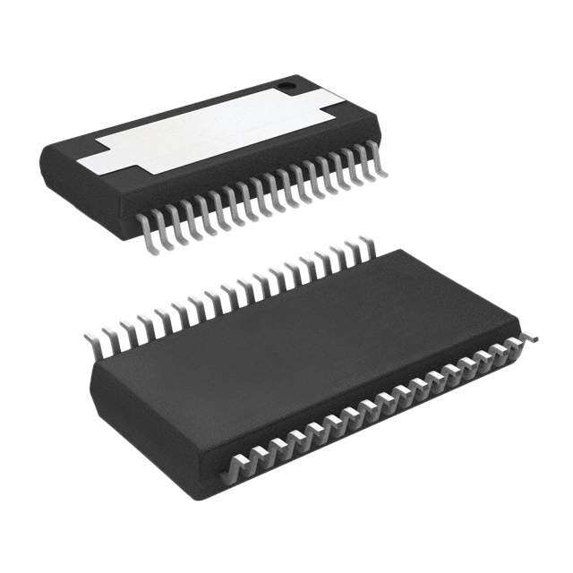
| 描述 | IC AMP AUDIO PWR 48HTSSOP音频放大器 Closed Loop I2S Input Amp |
| 产品分类 | |
| 品牌 | Texas Instruments |
| 产品手册 | http://www.ti.com/lit/gpn/tas5760md |
| 产品图片 |
|
| rohs | 符合RoHS无铅 / 符合限制有害物质指令(RoHS)规范要求 |
| 产品系列 | 音频 IC,音频放大器,Texas Instruments TAS5760MDDCA- |
| 数据手册 | |
| 产品型号 | TAS5760MDDCA |
| THD+噪声 | 0.04 % |
| 不同负载时的最大输出功率x通道数 | 55.2W x 1 @ 4 欧姆, 63.5W x 2 @ 4 欧姆 |
| 产品 | Audio Amplifiers |
| 产品种类 | 音频放大器 |
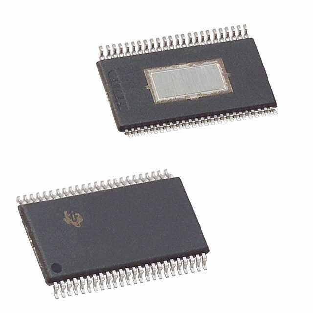
| 供应商器件封装 | 48-HTSSOP |
| 其它名称 | 296-36487-5 |
| 包装 | 管件 |
| 商标 | Texas Instruments |
| 增益 | 30 dBV |
| 安装类型 | 表面贴装 |
| 安装风格 | SMD/SMT |
| 封装 | Tube |
| 封装/外壳 | 48-TFSOP(0.240",6.10mm 宽)裸焊盘 |
| 封装/箱体 | HTSSOP-48 |
| 工作温度 | -25°C ~ 85°C (TA) |
| 工作电源电压 | 4.5 V to 26.4 V |
| 工厂包装数量 | 40 |
| 最大工作温度 | + 85 C |
| 最小工作温度 | - 25 C |
| 标准包装 | 40 |
| 特性 | 消除爆音 |
| 电压-电源 | 3 V ~ 3.6 V |
| 电源电压-最大 | 26.4 V |
| 电源电压-最小 | 4.5 V |
| 电源类型 | Single |
| 类 | Class-D |
| 类型 | D 类 |
| 系列 | TAS5760MD |
| 输入信号类型 | Stereo |
| 输出信号类型 | Digital |
| 输出功率 | 55.2 W |
| 输出类型 | 1-通道(单声道)或 2-通道(立体声) |


- 商务部:美国ITC正式对集成电路等产品启动337调查
- 曝三星4nm工艺存在良率问题 高通将骁龙8 Gen1或转产台积电
- 太阳诱电将投资9.5亿元在常州建新厂生产MLCC 预计2023年完工
- 英特尔发布欧洲新工厂建设计划 深化IDM 2.0 战略
- 台积电先进制程称霸业界 有大客户加持明年业绩稳了
- 达到5530亿美元!SIA预计今年全球半导体销售额将创下新高
- 英特尔拟将自动驾驶子公司Mobileye上市 估值或超500亿美元
- 三星加码芯片和SET,合并消费电子和移动部门,撤换高东真等 CEO
- 三星电子宣布重大人事变动 还合并消费电子和移动部门
- 海关总署:前11个月进口集成电路产品价值2.52万亿元 增长14.8%


PDF Datasheet 数据手册内容提取
Product Order Technical Tools & Support & Folder Now Documents Software Community TAS5760MD SLOS741D–MAY2013–REVISEDMAY2017 TAS5760MD General-Purpose I2S Input Class-D Amplifier With DirectPath™ Headphone and Line Driver 1 Features 3 Description • AudioI/OConfiguration: The TAS5760MD is a stereo I2S input device which 1 includes hardware and software (I²C) control modes, – SingleStereoI²SInput integrated digital clipper, several gain options, and a – StereoBridgeTiedLoad(BTL)orMono wide power supply operating range to enable use in a ParallelBridgeTiedLoad(PBTL)Operation multitude of applications. The TAS5760MD operates with a nominal supply voltage from 4.5 to 24 VDC. – 32,44.1,48,88.2,96kHzSampleRates The device has an integrated DirectPath™ – HeadphoneAmplifier/LineDriver headphone amplifier and line driver to increase • GeneralOperationalFeatures: system level integration and reduce total solution – SelectableHardwareorSoftwareControl costs. – IntegratedDigitalOutputClipper An optimal mix of thermal performance and device – ProgrammableI²CAddress(1101100[R ]or cost is provided in the 120-mΩ RDS(ON) of the output /W 1101101[R ]) MOSFETs. Additionally, a thermally enhanced 48-Pin /W TSSOP provides excellent operation in the elevated – Closed-LoopAmplifierArchitecture ambient temperatures found in modern consumer – AdjustableSwitchingFrequencyforSpeaker electronicdevices. Amplifier The entire TAS5760xx family is pin-to-pin compatible • RobustnessFeatures: in the 48-Pin TSSOP package. Alternatively, to – ClockError,DC,andShort-CircuitProtection achieve the smallest possible solutions size for applications where pin-to-pin compatibility and a – OvertemperatureandProgrammable headphone or line driver are not required, a 32-Pin OvercurrentProtection TSSOP package is offered for the TAS5760M and • AudioPerformance(PVDD=19V,RSPK =8 Ω, TAS5760L devices. The I2C register map in all of the SPK_GAIN[1:0]Pins=01) TAS5760xx devices are identical, to ensure low – IdleChannelNoise= <80µVrms(A-Wtd) development overhead when choosing between devicesbaseduponsystem-levelrequirements. – THD+N=0.03%(at1W,1kHz) – SNR=100dBA-Wtd(Ref.toTHD+N=1%) DeviceInformation(1) PARTNUMBER PACKAGE BODYSIZE(NOM) 2 Applications TAS5760MD HTSSOP(48) 12.50mm×6.10mm • LCD/LEDTVandMultipurposeMonitors (1) For all available packages, see the orderable addendum at • SoundBars,DockingStations,PCAudio theendofthedatasheet. • General-PurposeAudioEquipment FunctionalBlockDiagram Powerat10%THD+NvsPVDD DVDD DRVDD ANA_REG AVDD PVDD GVDD_REG 50 SVInuotpeltpranlgieaesl DRVDD InterRneagl uRlaetfoerrsence DIrnivteer nRaelg Gualatteo r W) 4405 RRRLLL === 468 WWW SFT_MLSSCRCCDLCLLIINPKKK SAPeuordiraitol VCDBooiolg&nuoitmtsraotel l CDliigpiptaelr CDoAniPGgnvWiaatealirMonls gti oo nClosCedSlip oLpfote orp ClassDD GGDrriiaavv Atteeeemss plifierPPFFoouuwwllllee BBrrBA rrSSiiddttaaggggeeee PCroOutverrecertni-otn SSSSPPPPKKKK____OOOOUUUUTTTTBABA++-- utput Power ( 233505 684 WWW TTThhheeerrrmmmaaalll LLLiiimmmiiittt O m 20 DDDDRRRR____IIIINNNNBABA++-- CDeinretecLrtePindae tHC hDeTloMraic vdGkep rrMhoouonnnedit o / ring ChDarRgVeD PDump Internal Control Registers and State MachTineemspD. Mieonitor Maximu 1105 5 DR_OUTA DR_OUTB DRVSSDR_CPDR_CN PSBCTLL/SPK_GAIN0SPK_GAIN1SPK_SDSPK_FAULTSPKA_SDLREEP/FSRDEAQ/ THD+N = 10% 0 4 6 8 10 12 14 16 18 20 22 24 26 Supply Voltage (V) G001 NOTE: Thermal Limits were determined via the TAS5760xxEVM 1 An IMPORTANT NOTICE at the end of this data sheet addresses availability, warranty, changes, use in safety-critical applications, intellectualpropertymattersandotherimportantdisclaimers.PRODUCTIONDATA.
TAS5760MD SLOS741D–MAY2013–REVISEDMAY2017 www.ti.com Table of Contents 1 Features.................................................................. 1 7.17 TypicalCharacteristics(MonoPBTLMode): f =384kHz..................................................24 2 Applications........................................................... 1 SPK_AMP 7.18 TypicalCharacteristics(MonoPBTLMode): 3 Description............................................................. 1 f =768kHz..................................................25 SPK_AMP 4 RevisionHistory..................................................... 2 8 DetailedDescription............................................ 27 5 DeviceComparisonTable..................................... 4 8.1 Overview.................................................................27 6 PinConfigurationandFunctions......................... 4 8.2 FunctionalBlockDiagram.......................................27 7 Specifications......................................................... 6 8.3 FeatureDescription.................................................28 7.1 AbsoluteMaximumRatings .....................................6 8.4 DeviceFunctionalModes........................................33 7.2 ESDRatings..............................................................6 8.5 RegisterMaps.........................................................41 7.3 RecommendedOperatingConditions.......................6 9 ApplicationandImplementation........................ 48 7.4 ThermalInformation..................................................7 9.1 ApplicationInformation............................................48 7.5 DigitalI/OPins..........................................................7 9.2 TypicalApplications................................................48 7.6 MasterClock.............................................................7 10 PowerSupplyRecommendations..................... 63 7.7 SerialAudioPort.......................................................8 10.1 DVDDSupply........................................................63 7.8 ProtectionCircuitry....................................................8 10.2 PVDDSupply........................................................63 7.9 SpeakerAmplifierinAllModes.................................8 11 Layout................................................................... 64 7.10 SpeakerAmplifierinStereoBridgeTiedLoad(BTL) 11.1 LayoutGuidelines.................................................64 Mode.......................................................................... 9 11.2 LayoutExample....................................................66 7.11 SpeakerAmplifierinMonoParallelBridgeTied Load(PBTL)Mode...................................................11 12 DeviceandDocumentationSupport................. 68 7.12 HeadphoneAmplifierandLineDriver ..................13 12.1 DocumentationSupport........................................68 7.13 I²CControlPort.....................................................14 12.2 CommunityResources..........................................68 7.14 TypicalIdle,Mute,Shutdown,OperationalPower 12.3 Trademarks...........................................................68 Consumption............................................................15 12.4 ElectrostaticDischargeCaution............................68 7.15 TypicalCharacteristics(StereoBTLMode): 12.5 Glossary................................................................68 fSPK_AMP=384kHz..................................................19 13 Mechanical,Packaging,andOrderable 7.16 TypicalCharacteristics(StereoBTLMode): Information........................................................... 68 f =768kHz..................................................21 SPK_AMP 4 Revision History NOTE:Pagenumbersforpreviousrevisionsmaydifferfrompagenumbersinthecurrentversion. ChangesfromRevisionC(September2014)toRevisionD Page • UpdatedtheRegisterMapsectiontothenewformat.Nonewdataadded......................................................................... 42 • Deletedstatementof64-kHzsamplerate............................................................................................................................ 43 ChangesfromRevisionB(July2013)toRevisionC Page • AddedPinConfigurationandFunctionssection,ESDRatingstable,FeatureDescriptionsection,DeviceFunctional Modes,ApplicationandImplementationsection,PowerSupplyRecommendationssection,Layoutsection,Device andDocumentationSupportsection,andMechanical,Packaging,andOrderableInformationsection .............................. 1 ChangesfromRevisionA(July2013)toRevisionB Page • ChangedFeatureslistitem,AudioPerformanceFrom:R =8ΩTo:R =8Ω.............................................................. 1 LOAD SPK • ChangedFrom:VoltageatspeakeramplifieroutputpinsTo:SpeakerAmplifierOutputVoltageintheAbsMaxtable.......6 • ChangedFigure30 .............................................................................................................................................................. 24 • ChangedtheSoftClipperControl(SFT_CLIPPin)section.................................................................................................. 34 • ChangedFigure64devicenumberreferenceFrom:TAS5760MDtoTAS5760xD............................................................. 51 • ChangedparagraphtextfollowingFigure64From:ThisisthearchitectureoftheTAS5760MD.To:Thisisthe architectureoftheheadphone/linedriverinsideoftheTAS5760MD................................................................................. 51 2 SubmitDocumentationFeedback Copyright©2013–2017,TexasInstrumentsIncorporated ProductFolderLinks:TAS5760MD
TAS5760MD www.ti.com SLOS741D–MAY2013–REVISEDMAY2017 ChangesfromOriginal(May2013)toRevisionA Page • ChangedtheProductPreviewdatasheet.............................................................................................................................. 1 Copyright©2013–2017,TexasInstrumentsIncorporated SubmitDocumentationFeedback 3 ProductFolderLinks:TAS5760MD
TAS5760MD SLOS741D–MAY2013–REVISEDMAY2017 www.ti.com 5 Device Comparison Table DEVICE DESCRIPTION PACKAGE Flexible,general-purposeI2Sinputclass-DAmplifierwith 48Pin,0.5-mmLead-Pitch,Pad-downTSSOP TAS5760MDDCA integratedheadphoneandlinedriverandintegrateddigital (DCA) clipper,whichsupportsPVDDlevels≤24V TAS5760MDCA 48Pin,0.5-mmLead-Pitch,Pad-downTSSOP Flexible,general-purposeI2Sinputclass-DAmplifierwith (DCA) TAS5760MDAP integrateddigitalclipper,whichsupportsPVDDlevels≤24V 32Pin,0.65mmLeadPitch,Pad-downTSSOP (DAP) Flexible,general-purposeI2Sinputclass-DAmplifierwith 48Pin,0.5-mmLead-Pitch,Pad-downTSSOP TAS5760LDDCA integratedheadphoneandlinedriverandintegrateddigital (DCA) clipper,whichsupportsPVDDlevels≤15V Flexible,general-purposeI2Sinputclass-DAmplifierwith integratedheadphoneandlinedriverandintegrateddigital 48Pin,0.5-mmLead-Pitch,Pad-downTSSOP TAS5760LD2DCA clipper,whichsupportsPVDDlevels≤15Vand3WireI²S (DCA) Mode. TAS5760LDCA 48Pin,0.5-mmLead-Pitch,Pad-downTSSOP Flexible,general-purposeI2Sinputclass-DAmplifierwith (DCA) integrateddigitalclipper,whichsupportsPVDDlevels≤15V TAS5760LDAP and3WireI²SMode. 32Pin,0.65-mmLeadPitch,Pad-downTSSOP (DAP) 6 Pin Configuration and Functions DCAPackage 48PinsTSSOP TopView SFT_CLIP 1 48 GVDD_REG ANA_REG 2 47 GGND VCOM 3 46 AVDD ANA_REF 4 45 PVDD SPK_FAULT 5 44 PVDD SPK_SD 6 43 BSTRPA+ FREQ/SDA 7 42 SPK_OUTA+ PBTL/SCL 8 41 PGND DVDD 9 40 SPK_OUTA- SPK_GAIN0 10 39 BSTRPA- SPK_GAIN1 11 38 BSTRPB- SPK_SLEEP/ADR 12 37 SPK_OUTB- MCLK 13 36 PGND SCLK 14 35 SPK_OUTB+ SDIN 15 34 BSTRPB+ LRCK 16 33 PVDD DGND 17 32 PVDD DR_INA- 18 PowerPAD 31 DR_INB- DR_INA+ 19 30 DR_INB+ DR_OUTA 20 29 DR_OUTB DRGND 21 28 DR_UVE DR_MUTE 22 27 DRGND DRVSS 23 26 DRVDD DR_CN 24 25 DR_CP PinFunctions PIN TYPE INTERNALTERMINATION DESCRIPTION NAME NO. AVDD 46 P - Powersupplyforinternalanalogcircuitry ConnectionpointforinternalreferenceusedbyANA_REGandVCOMfilter ANA_REF 4 P - capacitors. VoltageregulatorderivedfromAVDDsupply(NOTE:Thisterminalisprovided ANA_REG 2 P - asaconnectionpointforfilteringcapacitorsforthissupplyandmustnotbe usedtopoweranyexternalcircuitry) 4 SubmitDocumentationFeedback Copyright©2013–2017,TexasInstrumentsIncorporated ProductFolderLinks:TAS5760MD
TAS5760MD www.ti.com SLOS741D–MAY2013–REVISEDMAY2017 PinFunctions(continued) PIN TYPE INTERNALTERMINATION DESCRIPTION NAME NO. ConnectionpointfortheSPK_OUTA-bootstrapcapacitor,whichisusedto BSTRPA- 39 P - createapowersupplyforthehigh-sidegatedriveforSPK_OUTA- ConnectionpointfortheSPK_OUTA+bootstrapcapacitor,whichisusedto BSTRPA+ 43 P - createapowersupplyforthehigh-sidegatedriveforSPK_OUTA+ ConnectionpointfortheSPK_OUTB-bootstrapcapacitor,whichisusedto BSTRPB- 38 P - createapowersupplyforthehigh-sidegatedriveforSPK_OUTB- ConnectionpointfortheSPK_OUTB+bootstrapcapacitor,whichisusedto BSTRPB+ 34 P - createapowersupplyforthehigh-sidegatedriveforSPK_OUTB+ Groundfordigitalcircuitry(NOTE:Thisterminalshouldbeconnectedtothe DGND 17 G - systemground) Negativepinforcapacitorconnectionusedinheadphoneamplifier/linedriver DR_CN 24 P - chargepump Positivepinforcapacitorconnectionusedinheadphoneamplifier/linedriver DR_CP 25 P - chargepump DR_INA- 18 AI - NegativedifferentialinputforchannelAofheadphoneamplifier/linedriver DR_INA+ 19 AI - PositivedifferentialinputforchannelAofheadphoneamplifier/linedriver DR_INB- 31 AI - NegativedifferentialinputforchannelBofheadphoneamplifier/linedriver DR_INB+ 30 AI - PositivedifferentialinputforchannelBofheadphoneamplifier/linedriver DR_MUTE 22 DI - Placestheheadphoneamplifier/linedriverinmute DR_OUTA 20 AO - OutputforchannelAofheadphoneamplifier/linedriver DR_OUTB 29 AO - OutputforchannelBofheadphoneamplifier/linedriver Sensepinforunder-voltageprotectioncircuitfortheheadphoneamplifier/line DR_UVE 28 AI - driver NegativepowersupplygeneratedbychargepumpfromtheDRVDDsupplyfor DR_VSS 23 P - groundcenteredheadphone/linedriveroutput Groundforheadphoneamplifier/linedrivercircuitry(NOTE:Thisterminal DRGND 21 G - shouldbeconnectedtothesystemground) Groundforheadphoneamplifier/linedrivercircuitry(NOTE:Thisterminal DRGND 27 G - shouldbeconnectedtothesystemground) DRVDD 26 P - Powersupplyforinternalheadphone/linedrivercircuitry DVDD 9 P - Powersupplyfortheinternaldigitalcircuitry DualfunctionterminalthatfunctionsasanI²CdatainputpininI²CControl FREQ/SDA 7 DI WeakPulldown ModeorasaFrequencySelectterminalwheninHardwareControlMode. Groundforgatedrivecircuitry(NOTE:Thisterminalshouldbeconnectedto GGND 47 G - thesystemground) VoltageregulatorderivedfromPVDDsupply(NOTE:Thispinisprovidedasa GVDD_REG 48 P - connectionpointforfilteringcapacitorsforthissupplyandmustnotbeusedto poweranyexternalcircuitry) SerialAudioPortWordClock.Wordselectclockforthedigitalsignalthatis LRCK 16 DI WeakPulldown activeontheserialport'sinputdataline MasterClockusedforinternalclocktree,sub-circuit/statemachine,andSerial MCLK 13 DI WeakPulldown AudioPortclocking DualfunctionpinthatfunctionsasanI²CclockinputterminalinSoftware PBTL/SCL 8 DI WeakPulldown ControlModeorconfiguresthedevicetooperateinpre-filterParallelBridge TiedLoad(PBTL)modewheninHardwareControlMode Groundforpowerdevicecircuitry(NOTE:Thisterminalshouldbeconnected PGND 36,41 G - tothesystemground) 32,33, PVDD P - Powersupplyforinteralpowercircuitry 44,45 SerialAudioPortBitClock.Bitclockforthedigitalsignalthatisactiveonthe SCLK 14 DI WeakPulldown serialdataport'sinputdataline SDIN 15 DI WeakPulldown SerialAudioPortSerialDataIn.Datalinetotheserialdataport Sensepinwhichsetsthemaximumoutputvoltagebeforeclippingwhenthe SFT_CLIP 1 AI - softclippercircuitisactive Speakeramplifierfaultterminal,whichispulledLOWwhenaninternalfault SPK_FAULT 5 DO Open-Drain occurs SPK_GAIN0 10 DI WeakPulldown AdjuststheLSBofthemulti-bitgainofthespeakeramplifier SPK_GAIN1 11 DI WeakPulldown AdjuststheMSBofthemulti-bitgainofthespeakeramplifier Copyright©2013–2017,TexasInstrumentsIncorporated SubmitDocumentationFeedback 5 ProductFolderLinks:TAS5760MD
TAS5760MD SLOS741D–MAY2013–REVISEDMAY2017 www.ti.com PinFunctions(continued) PIN TYPE INTERNALTERMINATION DESCRIPTION NAME NO. SPK_SLEEP/AD InHardwareControlMode,placesthespeakeramplifierinsleepmode.In 12 DI WeakPullup R SoftwareControlMode,isusedtodeterminetheI²CAddressofthedevice SPK_OUTA- 40 AO - NegativepinfordifferentialspeakeramplifieroutputA SPK_OUTA+ 42 AO - PositivepinfordifferentialspeakeramplifieroutputA SPK_OUTB- 37 AO - NegativepinfordifferentialspeakeramplifieroutputB SPK_OUTB+ 35 AO - PositivepinfordifferentialspeakeramplifieroutputB SPK_SD 6 DI - Placesthespeakeramplifierinshutdown VCOM 3 P - BiasvoltageforinternalPWMconversionblock Providesbothelectricalandthermalconnectionfromthedevicetotheboard. AmatchinggroundpadmustbeprovidedonthePCBandthedevice PowerPAD™ - G - connectedtoitviasolder.Forproperelectricaloperation,thisgroundpad mustbeconnectedtothesystemground. 7 Specifications 7.1 Absolute Maximum Ratings overoperatingfree-airtemperaturerange(unlessotherwisenoted)(1) MIN MAX UNIT AmbientOperatingTemperature,T –25 85 °C A Temperature AmbientStorageTemperature,T –40 125 °C S AVDDSupply –0.3 30 V SupplyVoltage PVDDSupply –0.3 30 V DRVDDandDVDDSupply –0.3 4 V DVDDReferencedDigital DigitalInputsreferencedtoDVDDsupply –0.5 DVDD+0.5 V InputVoltages DRVDDReferencedDigital DigitalInputsreferencedtoDRVDDsupply –0.5 DRVDD+0.5 V InputVoltages HeadphoneLoad R 12.8 Ω HP LineDriverLoad R 600 Ω LD SpeakerAmplifierOutput V ,measuredattheoutputpin –0.3 32 V Voltage SPK_OUTxx Storagetemperaturerange,T –40 125 °C stg (1) StressesbeyondthoselistedunderAbsoluteMaximumRatingsmaycausepermanentdamagetothedevice.Thesearestressratings only,andfunctionaloperationofthedeviceattheseoranyotherconditionsbeyondthoseindicatedunderRecommendedOperating Conditionsisnotimplied.Exposuretoabsolute-maximum-ratedconditionsforextendedperiodsmayaffectdevicereliability. 7.2 ESD Ratings VALUE UNIT Humanbodymodel(HBM),perANSI/ESDA/JEDECJS-001(1) 4000 V(ESD) Electrostaticdischarge Charged-devicemodel(CDM),perJEDECspecificationJESD22- 1500 V C101(2) (1) JEDECdocumentJEP155statesthat500-VHBMallowssafemanufacturingwithastandardESDcontrolprocess. (2) JEDECdocumentJEP157statesthat250-VCDMallowssafemanufacturingwithastandardESDcontrolprocess. 7.3 Recommended Operating Conditions overoperatingfree-airtemperaturerange(unlessotherwisenoted) MIN NOM MAX UNIT T AmbientOperatingTemperature –25 85 °C A AVDD AVDDSupply 4.5 26.4 V PVDD PVDDSupply 4.5 26.4 V DRVDD,DVDD DRVDDandDVDDSupply 2.8 3.63 V 6 SubmitDocumentationFeedback Copyright©2013–2017,TexasInstrumentsIncorporated ProductFolderLinks:TAS5760MD
TAS5760MD www.ti.com SLOS741D–MAY2013–REVISEDMAY2017 Recommended Operating Conditions (continued) overoperatingfree-airtemperaturerange(unlessotherwisenoted) MIN NOM MAX UNIT InputLogicHIGHforDVDDandDRVDDReferenced VIH DVDD V (DR) DigitalInputs InputLogicLOWforDVDDandDRVDDReferenced VIL 0 V (DR) DigitalInputs R HeadphoneLoad 16 Ω HP R LineDriverLoad 1 Ω LD R MinimumSpeakerLoadinBTLMode 4 Ω SPK(BTL) R MinimumSpeakerLoadinPBTLMode 2 Ω SPK(PBTL) 7.4 Thermal Information TAS5760MD THERMALMETRIC(1) DCA[HTSSOP] DCA[HTSSOP] UNIT 48PIN(2) 48PIN(3) θ Junction-to-ambientthermalresistance 60.3 30.2 °C/W JA θ Junction-to-case(top)thermalresistance 16 14.3 °C/W JC(top) θ Junction-to-boardthermalresistance 12 12.7 °C/W JB ψ Junction-to-topcharacterizationparameter 0.4 0.6 °C/W JT ψ Junction-to-boardcharacterizationparameter 11.9 12.7 °C/W JB θ Junction-to-case(bottom)thermalresistance 0.8 0.7 °C/W JC(bottom) (1) Formoreinformationabouttraditionalandnewthermalmetrics,seetheSemiconductorandICPackageThermalMetricsapplication report,SPRA953. (2) JEDECStandard2LayerBoard (3) JEDECStandard4LayerBoard 7.5 Digital I/O Pins overoperatingfree-airtemperaturerange(unlessotherwisenoted) PARAMETER TESTCONDITIONS MIN TYP MAX UNIT InputLogicHIGHthresholdforDVDD Alldigitalpinsexceptfor V 70 %DVDD IH1 ReferencedDigitalInputs DR_MUTE InputLogicLOWthresholdforDVDD Alldigitalpinsexceptfor V 30 %DVDD IL1 ReferencedDigitalInputs DR_MUTE Alldigitalpinsexceptfor I InputLogicHIGHCurrentLevel 15 µA IH1 DR_MUTE Alldigitalpinsexceptfor I InputLogicLOWCurrentLevel –15 µA IL1 DR_MUTE V OutputLogicHIGHVoltageLevel I =2mA 90 %DVDD OH OH V OutputLogicLOWVoltageLevel I =-2mA 10 %DVDD OL OH InputLogicHIGHthresholdforDRVDD V ForDR_MUTEPin 60 %DRVDD IH2 ReferencedDigitalInputs InputLogicLOWthresholdforDRVDD V ForDR_MUTEPin 40 %DRVDD IL2 ReferencedDigitalInputs I InputLogicHIGHCurrentLevel ForDR_MUTEPin 1 µA IH2 I InputLogicLOWCurrentLevel ForDR_MUTEPin –1 µA IL2 7.6 Master Clock overoperatingfree-airtemperaturerange(unlessotherwisenoted) PARAMETER TESTCONDITIONS MIN TYP MAX UNIT D AllowableMCLKDutyCycle 45% 50% 55% MCLK Copyright©2013–2017,TexasInstrumentsIncorporated SubmitDocumentationFeedback 7 ProductFolderLinks:TAS5760MD
TAS5760MD SLOS741D–MAY2013–REVISEDMAY2017 www.ti.com Master Clock (continued) overoperatingfree-airtemperaturerange(unlessotherwisenoted) PARAMETER TESTCONDITIONS MIN TYP MAX UNIT Valuesinclude:128,192,256, f SupportedMCLKFrequencies 128 512 f MCLK 384,512. S 7.7 Serial Audio Port overoperatingfree-airtemperaturerange(unlessotherwisenoted) PARAMETER TESTCONDITIONS MIN TYP MAX UNIT D AllowableSCLKDutyCycle 45% 50% 55% SCLK RequiredLRCKtoSCLKRisingEdge 15 ns RequiredSDINHoldTimeafterSCLK t 15 ns HLD RisingEdge RequiredSDINSetupTimebeforeSCLK t 15 ns su RisingEdge Sampleratesabove48kHz supportedby"doublespeed f SupportedInputSampleRates 32 96 kHz S mode,"whichisactivated throughtheI²Ccontrolport f SupportedSCLKFrequencies Valuesinclude:32,48,64 32 64 f SCLK S 7.8 Protection Circuitry overoperatingfree-airtemperaturerange(unlessotherwisenoted) PARAMETER TESTCONDITIONS MIN TYP MAX UNIT OVE PVDDOvervoltageErrorThreshold PVDDRising 28 V RTHRES(PVDD) OVE PVDDOvervoltageErrorThreshold PVDDFalling 27.3 V FTHRES(PVDD) PVDDUndervoltageError(UVE) UVE PVDDFalling 3.95 V FTHRES(PVDD) Threshold UVE PVDDUVEThreshold(PVDDRising) PVDDRising 4.15 V RTHRES(PVDD) OvertemperatureError(OTE) OTE 150 °C THRES Threshold OvertemperatureError(OTE) OTE 15 °C HYST Hysteresis OvercurrentError(OCE)Thresholdfor OCE PVDD=15V,T =25°C 7 A THRES eachBTLOutput A DCE DCError(DCE)Threshold PVDD=12V,T =25°C 2.6 V THRES A SpeakerAmplifierFaultTimeOut DCDetectError 650 ms T SPK_FAULT period OTEorOCPFault 1.3 s UndervoltageError(UVE)Threshold UVE SensedonDR_UVEpin 1.25 V THRES(DRVDD) forheadphoneandlinedriveramplifier CurrentSourcingLimitofthe I 68 mA LIMIT(DR) Headphoneandlinedriveramplifier 7.9 Speaker Amplifier in All Modes overoperatingfree-airtemperaturerange(unlessotherwisenoted) PARAMETER TESTCONDITIONS MIN TYP MAX UNIT HardwareControlMode SpeakerAmplifierGainwith (Additionalgainsettings AV 25.2 dBV 00 SPK_GAIN[1:0]Pins=00 availableinSoftwareControl Mode)(1) (1) Thedigitalboostblockcontributes+6dBofgaintothisvalue.Theaudiosignalmustbekeptbelow-6dBtoavoidclippingthedigital audiopath. 8 SubmitDocumentationFeedback Copyright©2013–2017,TexasInstrumentsIncorporated ProductFolderLinks:TAS5760MD
TAS5760MD www.ti.com SLOS741D–MAY2013–REVISEDMAY2017 Speaker Amplifier in All Modes (continued) overoperatingfree-airtemperaturerange(unlessotherwisenoted) PARAMETER TESTCONDITIONS MIN TYP MAX UNIT HardwareControlMode SpeakerAmplifierGainwith (Additionalgainsettings AV 28.6 dBV 01 SPK_GAIN[1:0]Pins=01 availableinSoftwareControl Mode)(1) HardwareControlMode SpeakerAmplifierGainwith (Additionalgainsettings AV 31 dBV 10 SPK_GAIN[1:0]Pins=10 availableinSoftwareControl Mode)(1) SpeakerAmplifierGainwith (Thissettingplacesthedevice AV (SetviaI²C) 11 SPK_GAIN[1:0]Pins=11 inSoftwareControlMode) BTL,Worstcaseovervoltage, 10 mV |VOS| gainsettings (SPK_ SpeakerAmplifierDCOffset AMP) PBTL,Worstcaseovervoltage, 15 mV gainsettings (HardwareControlMode. SpeakerAmplifierSwitchingFrequency Additionalswitchingrates f 16 f SPK_AMP(0) whenPWM_FREQPin=0 availableinSoftwareControl S Mode.) (HardwareControlMode. SpeakerAmplifierSwitchingFrequency Additionalswitchingrates f 8 f SPK_AMP(1) whenPWM_FREQPin=1 availableinSoftwareControl S Mode.) PVDD=15V,TA=25°C,Die 120 mΩ Only OnResistanceofOutputMOSFET(both RDS(ON) high-sideandlow-side) PVDD=15V,TA=25°C, Includes:Die,BondWires, 150 mΩ Leadframe f =44.1kHz 3.7 S –3-dBCornerFrequencyofHigh-Pass fS=48kHz 4 f Hz C Filter f =88.2kHz 7.4 S f =96kHz 8 S 7.10 Speaker Amplifier in Stereo Bridge Tied Load (BTL) Mode Inputsignalis1kHzSine,specificationsareoveroperatingfree-airtemperaturerange(unlessotherwisenoted) PARAMETER TESTCONDITIONS MIN TYP MAX UNIT PVDD=12V,SPK_GAIN[1:0]Pins=00, 66 R =8Ω,A-Weighted SPK PVDD=15V,SPK_GAIN[1:0]Pins=01, 75 R =8Ω,A-Weighted SPK ICN IdleChannelNoise µVrms (SPK) PVDD=19V,SPK_GAIN[1:0]Pins=01, 79 R =8Ω,A-Weighted SPK PVDD=24V,SPK_GAIN[1:0]Pins=10, 120 R =8Ω,A-Weighted SPK Copyright©2013–2017,TexasInstrumentsIncorporated SubmitDocumentationFeedback 9 ProductFolderLinks:TAS5760MD
TAS5760MD SLOS741D–MAY2013–REVISEDMAY2017 www.ti.com Speaker Amplifier in Stereo Bridge Tied Load (BTL) Mode (continued) Inputsignalis1kHzSine,specificationsareoveroperatingfree-airtemperaturerange(unlessotherwisenoted) PARAMETER TESTCONDITIONS MIN TYP MAX UNIT PVDD=12V,SPK_GAIN[1:0]Pins=00, 14.2 R =4Ω,THD+N=0.1%, SPK PVDD=12V,SPK_GAIN[1:0]Pins=00, 8 R =8Ω,THD+N=0.1% SPK PVDD=15V,SPK_GAIN[1:0]Pins=01, 21.9 R =4Ω,THD+N=0.1%, SPK PVDD=15V,SPK_GAIN[1:0]Pins=01, 12.5 MaximumInstantaneous RSPK=8Ω,THD+N=0.1% Po W (SPK) OutputPowerPer.Ch. PVDD=19V,SPK_GAIN[1:0]Pins=01, 33.5 R =4Ω,THD+N=0.1%, SPK PVDD=19V,SPK_GAIN[1:0]Pins=01, 20 R =8Ω,THD+N=0.1% SPK PVDD=24V,SPK_GAIN[1:0]Pins=10, 55.2 R =4Ω,THD+N=0.1%, SPK PVDD=24V,SPK_GAIN[1:0]Pins=10, 31.8 R =8Ω,THD+N=0.1% SPK PVDD=12V,SPK_GAIN[1:0]Pins=00, 14 R =4Ω,THD+N=0.1%, SPK PVDD=12V,SPK_GAIN[1:0]Pins=00, 8 R =8Ω,THD+N=0.1% SPK PVDD=15V,SPK_GAIN[1:0]Pins=01, 13.25 R =4Ω,THD+N=0.1%, SPK PVDD=15V,SPK_GAIN[1:0]Pins=01, 12.5 MaximumContinuous RSPK=8Ω,THD+N=0.1% Po(SPK) OutputPowerPer.Ch.(1) PVDD=19V,SPK_GAIN[1:0]Pins=01, W 12.25 R =4Ω,THD+N=0.1%, SPK PVDD=19V,SPK_GAIN[1:0]Pins=01, 20 R =8Ω,THD+N=0.1% SPK PVDD=24V,SPK_GAIN[1:0]Pins=10, 11 R =4Ω,THD+N=0.1%, SPK PVDD=24V,SPK_GAIN[1:0]Pins=10, 24 R =8Ω,THD+N=0.1% SPK PVDD=12V,SPK_GAIN[1:0]Pins=00, 99.7 R =8Ω,A-Weighted,-60dBFSInput SPK PVDD=15V,SPK_GAIN[1:0]Pins=01, SignaltoNoiseRatio R =8Ω,A-Weighted,-60dBFSInput 98.2 SPK SNR (ReferencedtoTHD+N= dB (SPK) 1%) PVDD=19V,SPK_GAIN[1:0]Pins=01, 100.4 R =8Ω,A-Weighted,-60dBFSInput SPK PVDD=24V,SPK_GAIN[1:0]Pins=10, 98.8 R =8Ω,A-Weighted,-60dBFSInput SPK (1) Thecontinuouspoweroutputofanyamplifierisdeterminedbythethermalperformanceoftheamplifieraswellaslimitationsplacedon itbythesystemaroundit,suchasthePCBconfigurationandtheambientoperatingtemperature.Theperformancecharacteristicslisted inthissectionareachievableontheTAS5760MD'sEVM,whichisrepresentativeofthepoplular"2Layers/1ozCopper"PCB configurationinasizethatisrepresentativeoftheamountofareaoftenprovidedtotheamplifiersectionofpopularconsumeraudio electronics.Ascanbeseenintheinstantaneouspowerportionofthistable,morepowercanbedeliveredfromtheTAS5760MDifsteps aretakentopullmoreheatoutofthedevice.Forinstance,usingaboardwithmorelayersoraddingasmallheatsinkwillresultinan increaseofcontinuouspower,uptoandincludingtheinstantaneouspowerlevel.ThisbehaviorcanalsobeenseeninthePOUTvs. PVDDplotsshownintheTypicalCharacteristics(StereoBTLMode):f =384kHzsectionofthisdatasheet. SPK_AMP 10 SubmitDocumentationFeedback Copyright©2013–2017,TexasInstrumentsIncorporated ProductFolderLinks:TAS5760MD
TAS5760MD www.ti.com SLOS741D–MAY2013–REVISEDMAY2017 Speaker Amplifier in Stereo Bridge Tied Load (BTL) Mode (continued) Inputsignalis1kHzSine,specificationsareoveroperatingfree-airtemperaturerange(unlessotherwisenoted) PARAMETER TESTCONDITIONS MIN TYP MAX UNIT PVDD=12V,SPK_GAIN[1:0]Pins=00, 0.02% R =4Ω,Po=1W SPK PVDD=12V,SPK_GAIN[1:0]Pins=00, 0.03% R =8Ω,Po=1W SPK PVDD=15V,SPK_GAIN[1:0]Pins=01, 0.03% R =4Ω,Po=1W SPK PVDD=15V,SPK_GAIN[1:0]Pins=01, 0.03% TotalHarmonicDistortion RSPK=8Ω,Po=1W THD+N (SPK) andNoise PVDD=19V,SPK_GAIN[1:0]Pins=01, 0.03% R =4Ω,Po=1W SPK PVDD=19V,SPK_GAIN[1:0]Pins=01, 0.04% R =8Ω,Po=1W SPK PVDD=24V,SPK_GAIN[1:0]Pins=10, 0.03% R =4Ω,Po=1W SPK PVDD=24V,SPK_GAIN[1:0]Pins=10, 0.04% R =8Ω,Po=1W SPK PVDD=12V,SPK_GAIN[1:0]Pins=00, R =8Ω,InputSignal250mVrms,1kHz –92 SPK Sine PVDD=15V,SPK_GAIN[1:0]Pins=01, R =8Ω,InputSignal250mVrms,1kHz –93 SPK Cross-talk(worstcase Sine X-Talk betweenLtoRandRtoL dB (SPK) coupling) PVDD=19V,SPK_GAIN[1:0]Pins=01, R =8Ω,InputSignal250mVrms,1kHz –94 SPK Sine PVDD=24V,SPK_GAIN[1:0]Pins=10, R =8Ω,InputSignal250mVrms,1kHz –93 SPK Sine 7.11 Speaker Amplifier in Mono Parallel Bridge Tied Load (PBTL) Mode inputsignalis1kHzSine,specificationsareoveroperatingfree-airtemperaturerange(unlessotherwisenoted) PARAMETER TESTCONDITIONS MIN TYP MAX UNIT PVDD=12V,SPK_GAIN[1:0]Pins=00, 69 RSPK=8Ω,A-Weighted PVDD=15V,SPK_GAIN[1:0]Pins=01, 85 RSPK=8Ω,A-Weighted ICN IdleChannelNoise µVrms PVDD=19V,SPK_GAIN[1:0]Pins=01, 85 RSPK=8Ω,A-Weighted PVDD=24V,SPK_GAIN[1:0]Pins=10, 131 RSPK=8Ω,A-Weighted Copyright©2013–2017,TexasInstrumentsIncorporated SubmitDocumentationFeedback 11 ProductFolderLinks:TAS5760MD
TAS5760MD SLOS741D–MAY2013–REVISEDMAY2017 www.ti.com Speaker Amplifier in Mono Parallel Bridge Tied Load (PBTL) Mode (continued) inputsignalis1kHzSine,specificationsareoveroperatingfree-airtemperaturerange(unlessotherwisenoted) PARAMETER TESTCONDITIONS MIN TYP MAX UNIT PVDD=12V,SPK_GAIN[1:0]Pins=00, 28.6 RSPK=2Ω,THD+N=0.1%, PVDD=12V,SPK_GAIN[1:0]Pins=00, 15.9 RSPK=4Ω,THD+N=0.1%, PVDD=12V,SPK_GAIN[1:0]Pins=00, 8.4 RSPK=8Ω,THD+N=0.1% PVDD=15V,SPK_GAIN[1:0]Pins=01, 43.2 RSPK=2Ω,THD+N=0.1%, PVDD=15V,SPK_GAIN[1:0]Pins=01, 25 RSPK=4Ω,THD+N=0.1%, PVDD=15V,SPK_GAIN[1:0]Pins=01, 13.3 MaximumInstantaneousOutput RSPK=8Ω,THD+N=0.1% PO(SPK) Power PVDD=19V,SPK_GAIN[1:0]Pins=01, W 68.3 RSPK=2Ω,THD+N=0.1%, PVDD=19V,SPK_GAIN[1:0]Pins=01, 40 RSPK=4Ω,THD+N=0.1%, PVDD=19V,SPK_GAIN[1:0]Pins=01, 21.3 RSPK=8Ω,THD+N=0.1% PVDD=24V,SPK_GAIN[1:0]Pins=10, 114.7 RSPK=2Ω,THD+N=0.1%, PVDD=24V,SPK_GAIN[1:0]Pins=10, 63.5 RSPK=4Ω,THD+N=0.1%, PVDD=24V,SPK_GAIN[1:0]Pins=10, 34.1 RSPK=8Ω,THD+N=0.1% PVDD=12V,SPK_GAIN[1:0]Pins=00, 30 RSPK=2Ω,THD+N=0.1%, PVDD=12V,SPK_GAIN[1:0]Pins=00, 15.9 RSPK=4Ω,THD+N=0.1%, PVDD=12V,SPK_GAIN[1:0]Pins=00, 8.4 RSPK=8Ω,THD+N=0.1% PVDD=15V,SPK_GAIN[1:0]Pins=01, 28.5 RSPK=2Ω,THD+N=0.1%, PVDD=15V,SPK_GAIN[1:0]Pins=01, 25 RSPK=4Ω,THD+N=0.1%, PVDD=15V,SPK_GAIN[1:0]Pins=01, 13.3 MaximumContinuousOutput RSPK=8Ω,THD+N=0.1% PO(SPK) Power(1) PVDD=19V,SPK_GAIN[1:0]Pins=01, W 26.5 RSPK=2Ω,THD+N=0.1%, PVDD=19V,SPK_GAIN[1:0]Pins=01, 40 RSPK=4Ω,THD+N=0.1%, PVDD=19V,SPK_GAIN[1:0]Pins=01, 21.3 RSPK=8Ω,THD+N=0.1% PVDD=24V,SPK_GAIN[1:0]Pins=10, 24 RSPK=2Ω,THD+N=0.1%, PVDD=24V,SPK_GAIN[1:0]Pins=10, 40 RSPK=4Ω,THD+N=0.1%, PVDD=24V,SPK_GAIN[1:0]Pins=10, 34.1 RSPK=8Ω,THD+N=0.1% (1) Thecontinuouspoweroutputofanyamplifierisdeterminedbythethermalperformanceoftheamplifieraswellaslimitationsplacedon itbythesystemaroundit,suchasthePCBconfigurationandtheambientoperatingtemperature.Theperformancecharacteristicslisted inthissectionareachievableontheTAS5760MD'sEVM,whichisrepresentativeofthepoplular"2Layers/1ozCopper"PCB configurationinasizethatisrepresentativeoftheamountofareaoftenprovidedtotheamplifiersectionofpopularconsumeraudio electronics.Ascanbeseenintheinstantaneouspowerportionofthistable,morepowercanbedeliveredfromtheTAS5760MDifsteps aretakentopullmoreheatoutofthedevice.Forinstance,usingaboardwithmorelayersoraddingasmallheatsinkwillresultinan increaseofcontinuouspower,uptoandincludingtheinstantaneouspowerlevel.ThisbehaviorcanalsobeenseeninthePOUTvs. PVDDplotsshownintheTypicalCharacteristics(MonoPBTLMode):f =384kHzsectionofthisdatasheet. SPK_AMP 12 SubmitDocumentationFeedback Copyright©2013–2017,TexasInstrumentsIncorporated ProductFolderLinks:TAS5760MD
TAS5760MD www.ti.com SLOS741D–MAY2013–REVISEDMAY2017 Speaker Amplifier in Mono Parallel Bridge Tied Load (PBTL) Mode (continued) inputsignalis1kHzSine,specificationsareoveroperatingfree-airtemperaturerange(unlessotherwisenoted) PARAMETER TESTCONDITIONS MIN TYP MAX UNIT PVDD=12V,SPK_GAIN[1:0]Pins=00, 100.4 RSPK=8Ω,A-Weighted,-60dBFSInput PVDD=15V,SPK_GAIN[1:0]Pins=01, 99.5 SignaltoNoiseRatio(Referenced RSPK=8Ω,A-Weighted,-60dBFSInput SNR dB toTHD+N=1%) PVDD=19V,SPK_GAIN[1:0]Pins=01, 100.1 RSPK=8Ω,A-Weighted,-60dBFSInput PVDD=24V,SPK_GAIN[1:0]Pins=10, 99.5 RSPK=8Ω,A-Weighted,-60dBFSInput PVDD=12V,SPK_GAIN[1:0]Pins=00, 0.03% RSPK=2Ω,Po=1W PVDD=12V,SPK_GAIN[1:0]Pins=00, 0.02% RSPK=4Ω,Po=1W PVDD=12V,SPK_GAIN[1:0]Pins=00, 0.02% RSPK=8Ω,Po=1W PVDD=15V,SPK_GAIN[1:0]Pins=01, 0.03% RSPK=2Ω,Po=1W PVDD=15V,SPK_GAIN[1:0]Pins=01, 0.02% RSPK=4Ω,Po=1W PVDD=15V,SPK_GAIN[1:0]Pins=01, 0.02% TotalHarmonicDistortionand RSPK=8Ω,Po=1W THD+N(SPK) Noise PVDD=19V,SPK_GAIN[1:0]Pins=01, 0.03% RSPK=2Ω,Po=1W PVDD=19V,SPK_GAIN[1:0]Pins=01, 0.02% RSPK=4Ω,Po=1W PVDD=19V,SPK_GAIN[1:0]Pins=01, 0.03% RSPK=8Ω,Po=1W PVDD=24V,SPK_GAIN[1:0]Pins=10, 0.03% RSPK=2Ω,Po=1W PVDD=24V,SPK_GAIN[1:0]Pins=10, 0.02% RSPK=4Ω,Po=1W PVDD=24V,SPK_GAIN[1:0]Pins=10, 0.03% RSPK=8Ω,Po=1W 7.12 Headphone Amplifier and Line Driver inputsignalis1kHzSine,specificationsareoveroperatingfree-airtemperaturerange(unlessotherwisenoted) PARAMETER TESTCONDITIONS MIN TYP MAX UNIT InputtoOutputAttenuationwhenmuted 80 dB OutputOffsetVoltageofHeadphone |VOS| 0.5 mV (DR) AmplifierandLineDriver f ChargePumpSwitchingFrequency 200 300 400 kHz CP ICN IdleChannelNoise R =32Ω,A-Weighted 13 µVrms (HP) (HP) ICN IdleChannelNoise R =3kΩ,A-Weighted 11 µVrms (LD) (LD) R =16Ω,THD+N=1%, Po HeadphoneAmplifierOutputPower (HP) 40 mW (HP) OutputsinPhase PowerSupplyRejectionRatioof PSRR 80 dB (DR) HeadphoneAmplifierandLineDriver (Referencedto25mWOutput SNR SignaltoNoiseRatio Signal),R =16Ω,A- 96 dB (HP) (HP) Weighted (Referencedto2VrmsOutput SNR SignaltoNoiseRatio Signal),R =3kΩ,A- 90 105 dB (LD) (LD) Weighted TotalHarmonicDistortionandNoisefor THD+N(HP) P =10mW 0.01% theHeadphoneAmplifier O(HP) TotalHarmonicDistortionandNoisefor THD+N V =2Vrms 0.002% (LD) theLineDriver O(LD) Copyright©2013–2017,TexasInstrumentsIncorporated SubmitDocumentationFeedback 13 ProductFolderLinks:TAS5760MD
TAS5760MD SLOS741D–MAY2013–REVISEDMAY2017 www.ti.com Headphone Amplifier and Line Driver (continued) inputsignalis1kHzSine,specificationsareoveroperatingfree-airtemperaturerange(unlessotherwisenoted) PARAMETER TESTCONDITIONS MIN TYP MAX UNIT THD+N=1%,R =3kΩ, Vo LineDriverOutputVoltage (LD) 2 2.4 Vrms (LD) OutputsinPhase Cross-talk(worstcasebetweenLtoR X-Talk P =20mW –90 dB (HP) andRtoLcoupling) O(HP) Cross-talk(worstcasebetweenLtoR X-Talk Vo=1Vrms –111 dB (LD) andRtoLcoupling) Z OutputImpedancewhenmuted DR_MUTE=LOW 110 mΩ O(DR) CurrentdrawnfromDRVDDsupplyin I DR_MUTE=LOW 12 mA MUTE(DR) mute CurrentdrawnfromDRVDDsupplywith DR_MUTE=HIGH,P =25 I O(HP) 60 mA DRVDD(HP) headphone mW,Input=1kHz CurrentdrawnfromDRVDDsupplywith DR_MUTE=HIGH,V =2 I O(LD) 12 mA DRVDD(LD) linedriver Vrms,Input=1kHz 7.13 I²C Control Port specificationsareoveroperatingfree-airtemperaturerange(unlessotherwisenoted) PARAMETER TESTCONDITIONS MIN TYP MAX UNIT C AllowableLoadCapacitanceforEachI²C 400 pF L(I²C) Line f SupportSCLfrequency NoWaitStates 400 kHz SCL t BusFreetimebetweenSTOPand 1.3 µS buf STARTconditions t RiseTime,SCLandSDA 300 ns f(I²C) t HoldTime,SCLtoSDA 0 ns h1(I²C) t HoldTime,STARTconditiontoSCL 0.6 µs h2(I²C) t I²CStartupTime 12 mS I²C(start) t RiseTime,SCLandSDA 300 ns r(I²C) t SetupTime,SDAtoSCL 100 ns su1(I²C) t SetupTime,SCLtoSTARTcondition 0.6 µS su2(I²C) t SetupTime,SCLtoSTOPcondition 0.6 µS su3(I²C) T RequiredPulseDuration,SCLHIGH 0.6 µS w(H) T RequiredPulseDuration,SCLLOW 1.3 µS w(L) 14 SubmitDocumentationFeedback Copyright©2013–2017,TexasInstrumentsIncorporated ProductFolderLinks:TAS5760MD
TAS5760MD www.ti.com SLOS741D–MAY2013–REVISEDMAY2017 7.14 Typical Idle, Mute, Shutdown, Operational Power Consumption inputsignalis1kHzSine,specificationsareoveroperatingfree-airtemperaturerange(unlessotherwisenoted) V R I I P PVDD SPK SPEAKERAMPLIFIERSTATE PVDD+AVDD DVDD DISS [V] [Ω] [mA] [mA] [W] 4 23.48 3.73 0.15 Idle 8 23.44 3.72 0.15 4 23.53 3.72 0.15 Mute 8 f = 23.46 3.72 0.15 SPK_AMP 4 384kHz 13.26 0.48 0.08 Sleep 8 13.27 0.53 0.08 4 0.046 0.04 0 Shutdown 8 0.046 0.03 0 4 30.94 3.71 0.2 Idle 8 30.94 3.71 0.2 4 29.37 3.71 0.19 Mute 8 f = 29.39 3.71 0.19 6 SPK_AMP 4 768kHz 13.24 0.5 0.08 Sleep 8 13.23 0.52 0.08 4 0.046 0.03 0 Shutdown 8 0.046 0.03 0 4 39.39 3.7 0.25 Idle 8 39.43 3.7 0.25 4 36.91 3.7 0.23 Mute 8 f = 36.9 3.69 0.23 SPK_AMP 4 1152kHz 13.17 0.53 0.08 Sleep 8 13.13 0.45 0.08 4 0.046 0.03 0 Shutdown 8 0.046 0.03 0 Copyright©2013–2017,TexasInstrumentsIncorporated SubmitDocumentationFeedback 15 ProductFolderLinks:TAS5760MD
TAS5760MD SLOS741D–MAY2013–REVISEDMAY2017 www.ti.com Typical Idle, Mute, Shutdown, Operational Power Consumption (continued) inputsignalis1kHzSine,specificationsareoveroperatingfree-airtemperaturerange(unlessotherwisenoted) V R I I P PVDD SPK SPEAKERAMPLIFIERSTATE PVDD+AVDD DVDD DISS [V] [Ω] [mA] [mA] [W] 4 32.95 3.74 0.41 Idle 8 32.93 3.73 0.41 4 32.98 3.73 0.41 Mute 8 f = 32.97 3.73 0.41 SPK_AMP 4 384kHz 12.71 0.47 0.15 Sleep 8 12.75 0.5 0.15 4 0.053 0.04 0 Shutdown 8 0.053 0.04 0 4 44.84 3.73 0.55 Idle 8 44.82 3.73 0.55 4 42.71 3.72 0.52 Mute 8 f = 42.66 3.72 0.52 12 SPK_AMP 4 768kHz 12.71 0.49 0.15 Sleep 8 12.73 0.52 0.15 4 0.063 0.03 0 Shutdown 8 0.053 0.03 0 4 59.3 3.73 0.72 Idle 8 59.3 3.73 0.72 4 55.74 3.72 0.68 Mute 8 f = 55.74 3.72 0.68 SPK_AMP 4 1152kHz 12.67 0.49 0.15 Sleep 8 12.61 0.43 0.15 4 0.053 0.02 0 Shutdown 8 0.053 0.03 0 16 SubmitDocumentationFeedback Copyright©2013–2017,TexasInstrumentsIncorporated ProductFolderLinks:TAS5760MD
TAS5760MD www.ti.com SLOS741D–MAY2013–REVISEDMAY2017 Typical Idle, Mute, Shutdown, Operational Power Consumption (continued) inputsignalis1kHzSine,specificationsareoveroperatingfree-airtemperaturerange(unlessotherwisenoted) V R I I P PVDD SPK SPEAKERAMPLIFIERSTATE PVDD+AVDD DVDD DISS [V] [Ω] [mA] [mA] [W] 4 42 3.73 0.81 Idle 8 41.92 3.73 0.81 4 41.93 3.73 0.81 Mute 8 f = 41.97 3.72 0.81 SPK_AMP 4 384kHz 12.95 0.47 0.25 Sleep 8 13 0.52 0.25 4 0.072 0.04 0 Shutdown 8 0.072 0.03 0 4 55.86 3.73 1.07 Idle 8 55.82 3.73 1.07 4 51.72 3.72 0.99 Mute 8 f = 51.69 3.72 0.99 19 SPK_AMP 4 768kHz 12.96 0.47 0.25 Sleep 8 12.95 0.51 0.25 4 0.072 0.03 0 Shutdown 8 0.062 0.03 0 4 74.87 3.72 1.43 Idle 8 74.81 3.72 1.43 4 67.96 3.71 1.3 Mute 8 f = 67.91 3.71 1.3 SPK_AMP 4 1152kHz 12.94 0.51 0.25 Sleep 8 12.84 0.42 0.25 4 0.062 0.03 0 Shudown 8 0.062 0.03 0 Copyright©2013–2017,TexasInstrumentsIncorporated SubmitDocumentationFeedback 17 ProductFolderLinks:TAS5760MD
TAS5760MD SLOS741D–MAY2013–REVISEDMAY2017 www.ti.com Typical Idle, Mute, Shutdown, Operational Power Consumption (continued) inputsignalis1kHzSine,specificationsareoveroperatingfree-airtemperaturerange(unlessotherwisenoted) V R I I P PVDD SPK SPEAKERAMPLIFIERSTATE PVDD+AVDD DVDD DISS [V] [Ω] [mA] [mA] [W] 4 Idle 48.03 3.73 1.17 8 47.98 3.73 1.16 4 Mute 47.99 3.72 1.16 8 f = 48 3.72 1.16 SPK_AMP 4 384kHz Sleep 13.12 0.49 0.32 8 13.14 0.48 0.32 4 Shutdown 0.088 0.03 0 8 0.088 0.03 0 4 62.84 3.72 1.52 Idle 8 62.84 3.72 1.52 4 57.12 3.71 1.38 Mute 8 f = 57.07 3.71 1.38 24 SPK_AMP 4 768kHz 13.19 0.47 0.32 Sleep 8 13.14 0.49 0.32 4 0.078 0.03 0 Shutdown 8 0.078 0.03 0 4 84.86 3.71 2.05 Idle 8 84.83 3.71 2.05 4 75.07 3.7 1.81 Mute 8 f = 75.01 3.71 1.81 SPK_AMP 4 1152kHz 13.11 0.51 0.32 Sleep 8 13.03 0.43 0.31 4 0.078 0.03 0 Shutdown 8 0.078 0.03 0 18 SubmitDocumentationFeedback Copyright©2013–2017,TexasInstrumentsIncorporated ProductFolderLinks:TAS5760MD
TAS5760MD www.ti.com SLOS741D–MAY2013–REVISEDMAY2017 7.15 Typical Characteristics (Stereo BTL Mode): f = 384 kHz SPK_AMP AtT =25°C,f =384kHz,inputsignalis1kHzSine,unlessotherwisenoted.Filterusedfor8Ω=22µH+0.68µF, A SPK_AMP Filterusedfor6Ω=15µH+0.68µF,Filterusedfor4Ω=10µH+0.68µFunlessotherwisenoted. 50 10 W) 4405 RRRLLL === 468 WWW RRRLLL === 468 WWW wer ( 35 46 WW TThheerrmmaall LLiimmiitt 1 Po 30 8 W Thermal Limit %) m Output 2205 THD+N ( 0.1 mu 15 xi 0.01 a 10 M 5 THD+N = 10% 0 0.001 4 6 8 10 12 14 16 18 20 22 24 26 20 100 1k 10k 20k Supply Voltage (V) Frequency (Hz) G001 G024 ThermalLimitsarereferencedtoTAS5760xxEVMRevD PVDD=12V,P =1W OSPK Figure1.OutputPowervsPVDD Figure2.THD+NvsFrequency 10 160 RL = 4 W 150 RL = 6 W 140 RL = 8 W 130 1 120 %) MS) 110100 THD+N ( 0.00.11 Noise (µVR 5678900000 CChh12 IICCNN @@ GGaaiinn == 0000 40 Ch1 ICN @ Gain = 01 30 Ch2 ICN @ Gain = 01 20 Idle Channel Ch1 ICN @ Gain = 10 0.001 10 RL = 8 W Ch2 ICN @ Gain = 10 20 100 1k 10k 20k 0 Frequency (Hz) 8 10 12 14 16 18 20 22 24 G025 PVDD=24V,POSPK=1W Supply Voltage (V) G026 Figure3.THD+NvsFrequency Figure4.IdleChannelNoisevsPVDD 10 10 RL = 4 W RL = 6 W RL = 8 W 1 1 %) %) +N ( 0.1 +N ( 0.1 D D H H T T 0.01 0.01 RL = 4W RL = 6W RL = 8W 0.001 0.001 0.01 0.1 1 10 50 0.01 0.1 1 10 50 Output Power (W) Output Power (W) G027 G028 PVDD=12V,BothChannelsDriven PVDD=18V,BothChannelsDriven Figure5.THD+NvsOutputPower Figure6.THD+NvsOutputPower Copyright©2013–2017,TexasInstrumentsIncorporated SubmitDocumentationFeedback 19 ProductFolderLinks:TAS5760MD
TAS5760MD SLOS741D–MAY2013–REVISEDMAY2017 www.ti.com Typical Characteristics (Stereo BTL Mode): f = 384 kHz (continued) SPK_AMP AtT =25°C,f =384kHz,inputsignalis1kHzSine,unlessotherwisenoted.Filterusedfor8Ω=22µH+0.68µF, A SPK_AMP Filterusedfor6Ω=15µH+0.68µF,Filterusedfor4Ω=10µH+0.68µFunlessotherwisenoted. 10 100 RRLL == 46 WW 95 RL = 8 W RL = 8 W 90 1 %) 85 %) y ( THD+N ( 0.1 er Efficienc 778050 w 0.01 o 65 P 60 PVDD = 12 V PVDD = 18 V 55 0.001 PVDD = 24 V 0.01 0.1 1 10 80 50 Output Power (W) 0 5 10 15 20 25 30 35 40 45 50 55 60 G029 PVDD=24V,BothChannelsDriven Total Output Power (W) G030 Figure7.THD+NvsOutputPower Figure8.EfficiencyvsOutputPower 0 0 −10 PVCC = 24 V Right−to−Left RL = 8 W PVDD = 12 V −20 RL = 4 W Left−to−Right −10 PVDD = 18 V −30 −20 PVDD = 24 V −40 alk (dB) −−−765000 R (dB) −−4300 Crosst −−9800 PSR −−6500 −100 −110 −70 −120 −80 −130 −140 −90 20 100 1k 10k 20k 20 100 1k 10k 20k Frequency (Hz) Frequency (Hz) G031 G019 Figure9.CrosstalkvsFrequency Figure10.PVDDPSRRvsFrequency 0 40 RL = 8 W PVDD = 12 V RL = 8 W −10 DVDD = 3.3 V + 200 mVP-P PVDD = 18 V −20 PVDD = 24 V 35 −30 R (dB) −40 nt (mA) 30 PSR −−6500 Curre 25 −70 −80 −90 20 20 100 1k 10k 20k 8 10 12 14 16 18 20 22 24 Frequency (Hz) PVDD (V) G020 G042 Figure11.DVDDPSRRvsFrequency Figure12.IdleCurrentDrawvsPVDD(Filterless) 20 SubmitDocumentationFeedback Copyright©2013–2017,TexasInstrumentsIncorporated ProductFolderLinks:TAS5760MD
TAS5760MD www.ti.com SLOS741D–MAY2013–REVISEDMAY2017 Typical Characteristics (Stereo BTL Mode): f = 384 kHz (continued) SPK_AMP AtT =25°C,f =384kHz,inputsignalis1kHzSine,unlessotherwisenoted.Filterusedfor8Ω=22µH+0.68µF, A SPK_AMP Filterusedfor6Ω=15µH+0.68µF,Filterusedfor4Ω=10µH+0.68µFunlessotherwisenoted. 40 60 RL = 8 W RL = 8 W 55 35 mA) A) 50 ent ( 30 nt (µ Curr urre 45 C 25 40 20 8 10 12 14 16 18 20 22 24 35 PVDD (V) 8 10 12 14 16 18 20 22 24 G023 WithLCFilterasShownontheEVM PVDD (V) G022 Figure13.IdleCurrentDrawvsPVDD Figure14.ShutdownCurrentDrawvsPVDD(Filterless) 7.16 Typical Characteristics (Stereo BTL Mode): f = 768 kHz SPK_AMP AtT =25°C,f =768kHz,inputsignalis1kHzSine,unlessotherwisenoted.Filterusedfor8Ω=22µH+0.68µF, A SPK_AMP Filterusedfor6Ω=15µH+0.68µF,Filterusedfor4Ω=10µH+0.68µFunlessotherwisenoted. 50 10 W) 4405 RRRLLL === 468 WWW RRRLLL === 468 WWW wer ( 35 46 WW TThheerrmmaall LLiimmiitt 1 Po 30 8 W Thermal Limit %) m Output 2205 THD+N ( 0.1 mu 15 xi 0.01 a 10 M 5 THD+N = 10% 0 0.001 4 6 8 10 12 14 16 18 20 22 24 26 20 100 1k 10k 20k Supply Voltage (V) Frequency (Hz) G039 G002 ThermalLimitsarereferencedtoTAS5760xxEVMRevD PVDD=12V,P =1W OSPK Figure15.OutputPowervsPVDD Figure16.THD+NvsFrequency 10 130 RRRLLL === 468 WWW 111200 IRdLle = C 8h Wannel 1 100 90 %) MS) 80 THD+N ( 0.00.11 Noise (µVR 45670000 CChh12 IICCNN @@ GGaaiinn == 0000 Ch1 ICN @ Gain = 01 30 Ch2 ICN @ Gain = 01 20 Ch1 ICN @ Gain = 10 0.001 10 Ch2 ICN @ Gain = 10 20 100 1k 10k 20k 0 Frequency (Hz) 8 10 12 14 16 18 20 22 24 G003 PVDD=24V,P =1W PVDD (V) OSPK G006 Figure17.THD+NvsFrequency Figure18.IdleChannelNoisevsPVDD Copyright©2013–2017,TexasInstrumentsIncorporated SubmitDocumentationFeedback 21 ProductFolderLinks:TAS5760MD
TAS5760MD SLOS741D–MAY2013–REVISEDMAY2017 www.ti.com Typical Characteristics (Stereo BTL Mode): f = 768 kHz (continued) SPK_AMP AtT =25°C,f =768kHz,inputsignalis1kHzSine,unlessotherwisenoted.Filterusedfor8Ω=22µH+0.68µF, A SPK_AMP Filterusedfor6Ω=15µH+0.68µF,Filterusedfor4Ω=10µH+0.68µFunlessotherwisenoted. 10 10 RL = 4 W RL = 4 W RL = 6 W RL = 6 W RL = 8 W RL = 8 W 1 1 %) %) +N ( 0.1 +N ( 0.1 D D H H T T 0.01 0.01 0.001 0.001 0.01 0.1 1 10 30 0.01 0.1 1 10 40 Output Power per Channel (W) Output Power per Channel (W) G008 G009 PVDD=12V,BothChannelsDriven PVDD=18V,BothChannelsDriven Figure19.THD+NvsOutputPower Figure20.THD+NvsOutputPower 10 100 RRLL == 46 WW 95 RL = 8 W RL = 8 W 90 1 85 %) %) D+N ( 0.1 ncy ( 7850 TH Efficie 70 0.01 65 60 PVDD = 12 V PVDD = 18 V 55 0.001 PVDD = 24 V 0.01 0.1 1 10 60 50 Output Power per Channel (W) 0 5 10 15 20 25 30 G010 PVDD=24V,BothChannelsDriven Output Power per Channel (W) G014 Figure21.THD+NvsOutputPower Figure22.EfficiencyvsOutputPower 0 0 −10 PRVL D= D4 =W 24 V RLeigfth-tto-t-oR-Ligehftt −10 RL = 8 W PPVVDDDD == 1128 VV −20 −20 PVDD = 24 V −30 dB) −40 B) −30 alk ( −50 R (d −40 st −60 R −50 Cros −70 PS −60 −80 −70 −90 −100 −80 −110 −90 20 100 1k 10k 20k 20 100 1k 10k 20k Frequency (Hz) Frequency (Hz) G018 G019 Figure23.CrosstalkvsFrequency Figure24.PVDDPSRRvsFrequency 22 SubmitDocumentationFeedback Copyright©2013–2017,TexasInstrumentsIncorporated ProductFolderLinks:TAS5760MD
TAS5760MD www.ti.com SLOS741D–MAY2013–REVISEDMAY2017 Typical Characteristics (Stereo BTL Mode): f = 768 kHz (continued) SPK_AMP AtT =25°C,f =768kHz,inputsignalis1kHzSine,unlessotherwisenoted.Filterusedfor8Ω=22µH+0.68µF, A SPK_AMP Filterusedfor6Ω=15µH+0.68µF,Filterusedfor4Ω=10µH+0.68µFunlessotherwisenoted. 70 60 RL = 8 W RL = 8 W 65 55 60 50 A) 55 mA) 45 nt (m 50 ent ( 40 Curre 45 Curr 35 30 40 25 35 20 30 8 10 12 14 16 18 20 22 24 8 10 12 14 16 18 20 22 24 PVDD (V) G044 PVDD (V) WithLCFilterasShownonEVM G045 Figure25.IdleCurrentDrawvsPVDD(Filterless) Figure26.IdleCurrentDrawvsPVDD 60 RL = 8 W 55 A) 50 µ nt ( e urr 45 C 40 35 8 10 12 14 16 18 20 22 24 PVDD (V) G022 Figure27.ShutdownCurrentDrawvsPVDD(Filterless) Copyright©2013–2017,TexasInstrumentsIncorporated SubmitDocumentationFeedback 23 ProductFolderLinks:TAS5760MD
TAS5760MD SLOS741D–MAY2013–REVISEDMAY2017 www.ti.com 7.17 Typical Characteristics (Mono PBTL Mode): f = 384 kHz SPK_AMP AtT =25°C,f =384kHz,inputsignalis1kHzSineunlessotherwisenoted. A SPK_AMP 10 10 RL = 4 W RL = 2 W RL = 6 W RL = 4 W RL = 8 W RL = 6 W 1 1 RL = 8 W %) %) +N ( 0.1 +N ( 0.1 D D H H T T 0.01 0.01 0.001 0.001 20 100 1k 10k 20k 20 100 1k 10k 20k Frequency (Hz) Frequency (Hz) G032 G033 PVDD=12V,P =1W PVDD=24V,P =1W OSPK OSPK Figure28.THD+NvsFrequency Figure29.THD+NvsFrequency 160 10 150 RL = 2 W 140 RL = 4 W 130 RL = 6 W 120 1 RL = 8 W MS) 110100 %) µVR 8900 D+N ( 0.1 oise ( 6700 TH N 50 0.01 40 30 Gain = 00 20 Idle Channel Gain = 01 10 RL = 8 W Gain = 10 0.001 0 0.01 0.1 1 10 50 8 10 12 14 16 18 20 22 24 Output Power (W) G035 Supply Voltage (V) PVDD=12VWith1kHzSineInput G034 Figure30.IdleChannelNoisevsPVDD Figure31.THD+NvsOutputPower 10 10 RL = 2 W RL = 4 W RL = 6 W 1 RL = 8 W 1 %) %) +N ( 0.1 +N ( 0.1 D D H H T T 0.01 0.01 RL = 2 W RL = 4 W RL = 6 W RL = 8 W 0.001 0.001 0.01 0.1 1 10 100 0.01 0.1 1 10 100200 Output Power (W) Output Power (W) G036 G037 PVDD=18VWith1kHzSineInput PVDD=24VWith1kHzSineInput Figure32.THD+NvsOutputPower Figure33.THD+NvsOutputPower 24 SubmitDocumentationFeedback Copyright©2013–2017,TexasInstrumentsIncorporated ProductFolderLinks:TAS5760MD
TAS5760MD www.ti.com SLOS741D–MAY2013–REVISEDMAY2017 Typical Characteristics (Mono PBTL Mode): f = 384 kHz (continued) SPK_AMP AtT =25°C,f =384kHz,inputsignalis1kHzSineunlessotherwisenoted. A SPK_AMP 100 95 RL = 4 W 90 %) 85 y ( c 80 n e ci 75 Effi er 70 w o 65 P 60 PVDD = 12 V PVDD = 18 V 55 PVDD = 24 V 50 0 5 10 15 20 25 30 35 40 45 50 55 60 Total Output Power (W) G038 Figure34.EfficiencyvsOutputPower 7.18 Typical Characteristics (Mono PBTL Mode): f = 768 kHz SPK_AMP AtT =25°C,f =768kHz,inputsignalis1kHzSineunlessotherwisenoted. A SPK_AMP 10 10 RL = 4 W RL = 2 W RL = 6 W RL = 4 W RL = 8 W RL = 6 W 1 1 RL = 8 W %) %) +N ( 0.1 +N ( 0.1 D D H H T T 0.01 0.01 0.001 0.001 20 100 1k 10k 20k 20 100 1k 10k 20k Frequency (Hz) Frequency (Hz) G004 G005 PVDD=12V,P =1W PVDD=24V,P =1W OSPK OSPK Figure35.THD+NvsFrequency Figure36.THD+NvsFrequency 140 10 130 RL = 2 W 120 RL = 4 W 110 RL = 6 W 100 1 RL = 8 W MS) 90 %) µVR 7800 +N ( 0.1 oise ( 5600 THD N 40 0.01 30 ICN @ Gain = 00 20 Idle Channel ICN @ Gain = 01 10 RL = 8 W ICN @ Gain = 10 0 0.001 8 10 12 14 16 18 20 22 24 0.01 0.1 1 10 50 PVDD (V) Output Power (W) G007 G011 Figure37.IdleChannelNoisevsPVDD Figure38.THD+NvsOutputPowerWithPVDD=12V Copyright©2013–2017,TexasInstrumentsIncorporated SubmitDocumentationFeedback 25 ProductFolderLinks:TAS5760MD
TAS5760MD SLOS741D–MAY2013–REVISEDMAY2017 www.ti.com Typical Characteristics (Mono PBTL Mode): f = 768 kHz (continued) SPK_AMP AtT =25°C,f =768kHz,inputsignalis1kHzSineunlessotherwisenoted. A SPK_AMP 10 10 RL = 2 W RL = 2 W RL = 4 W RL = 4 W RL = 6 W RL = 6 W 1 RL = 8 W 1 RL = 8 W %) %) +N ( 0.1 +N ( 0.1 D D H H T T 0.01 0.01 0.001 0.001 0.01 0.1 1 10 100 0.01 0.1 1 10 100200 Output Power (W) Output Power (W) G012 G013 Figure39.THD+NvsOutputPowerWithPVDD=18V Figure40.THD+NvsOutputPowerWithPVDD=24V 100 95 RL = 4 W 90 85 %) y ( 80 nc 75 e Effici 70 65 60 PVDD = 12 V PVDD = 18 V 55 PVDD = 24 V 50 0 10 20 30 40 50 60 Output Power (W) G015 Figure41.EfficiencyvsOutputPower 26 SubmitDocumentationFeedback Copyright©2013–2017,TexasInstrumentsIncorporated ProductFolderLinks:TAS5760MD
TAS5760MD www.ti.com SLOS741D–MAY2013–REVISEDMAY2017 8 Detailed Description 8.1 Overview The TAS5760MD is a flexible and easy-to-use stereo class-D speaker amplifier with an I²S input serial audio port. The TAS5760MD device also includes a dual-purpose headphone and line driver, which features pop/click- less operation, great audio performance, variable gain setting, and minimal bill of materials. The TAS5760MD supportsavarietyofaudioclockconfigurationsviatwospeedmodes.InHardwareControlmode,thedeviceonly operates in single-speed mode. When used in Software Control mode, the device can be placed into double speed mode to support higher sample rates, such as 88.2 kHz and 96 kHz. The outputs of the TAS5760MD can beconfiguredtodrivetwospeakersinstereoBridgeTiedLoad(BTL)modeorasinglespeakerinParallelBridge TiedLoad(PBTL)mode. Only two power supplies are required for the TAS5760MD. They are a 3.3-V power supply, called VDD, for the small signal analog and digital and a higher voltage power supply, called PVDD, for the output stage of the speaker amplifier. To enable use in a variety of applications, PVDD can be operated over a large range of voltages,asspecifiedintheRecommendedOperatingConditions. To configure and control the TAS5760MD, two methods of control are available. In Hardware Control Mode, the configuration and real-time control of the device is accomplished through hardware control pins. In Software Control mode, the I²C control port is used both to configure the device and for real-time control. In Software Control Mode, several of the hardware control pins remain functional, such as the SPK_SD, SPK_FAULT, and SFT_CLIP pins. To allow the headphone amplifier / line driver to be used without needing the speaker amplifier tobeactive,hardwarecontrolsareprovidedfortheheadphoneamplifierviathe DR_MUTEandDR_UVEpins. 8.2 Functional Block Diagram DVDD DRVDD ANA_REG AVDD PVDD GVDD_REG Internal DRVDD Internal Reference Internal Gate Voltage Regulators Drive Regulator Supplies Closed Loop Class D Amplifier SFT_CLIP Digital to Full Bridge MCLK Digital PWM Gate Power Stage SPK_OUTA+ SCLK Serial Boost Digital Conversion Drives A Over- SPK_OUTA- Audio & Soft LRCK Clipper Current SDIN Port Volume Clipper Gate Protection SPK_OUTB+ Control Analog Drives Full Bridge Gain Power Stage SPK_OUTB- B Clock Monitoring Die DRVDD Temp. Monitor DR_INA+ DirectPathTM Ground DR_INA- Centered Headphone / DR_INB+ Line Driver Charge Pump Internal Control Registers and State Machines DR_INB- DR_OUTA DR_OUTB DRVSS DR_CP DR_CN PBTL/ SPK_GAIN0 SPK_GAIN1 SPK_SD SPK_FAULTSPK_SLEEP/FREQ/ SCL ADR SDA Figure42. FunctionalBlockDiagram Copyright©2013–2017,TexasInstrumentsIncorporated SubmitDocumentationFeedback 27 ProductFolderLinks:TAS5760MD
TAS5760MD SLOS741D–MAY2013–REVISEDMAY2017 www.ti.com Functional Block Diagram (continued) DR_INA+ DR_INB+ Line Line DR_INA– Driver Driver DR_INB– DR_OUTA DR_OUTB DRGND DR_UVP Clickand Pop Short-Circuit Suppression Protection DR_MUTE DRGND DRVSS Bias DRVDD Circuitry DR_CN DR_CP Figure43. FunctionalBlockDiagram:HeadphoneandLineDriverAmplifier 8.3 Feature Description 8.3.1 PowerSupplies The power supply requirements for the TAS5760MD consist of one 3.3-V supply to power the low voltage analog anddigitalcircuitryandonehigher-voltagesupplytopowertheoutput stage of the speaker amplifier. Several on- chip regulators are included on the TAS5760MD to generate the voltages necessary for the internal circuitry of the audio path. It is important to note that the voltage regulators which have been integrated are sized only to provide the current necessary to power the internal circuitry. The external pins are provided only as a connection point for off-chip bypass capacitors to filter the supply. Connecting external circuitry to these regulator outputs mayresultinreducedperformanceanddamagetothedevice. 8.3.2 SpeakerAmplifierAudioSignalPath Figure 44 shows a block diagram of the speaker amplifier of the TAS5760MD. In Hardware Control mode, a limited subset of audio path controls are made available via external pins, which are pulled HIGH or LOW to configure the device. In Software Control Mode, the additional features and configurations are available. All of the available controls are discussed in this section, and the subset of controls that available in Hardware Control Modearediscussedintherespectivesectionbelow. Digital Gain Analog Gain (G ) (G ) DIG ANA Closed Loop Class D Amplifier HPF Interpolation Digital Full Bridge Digital Filter Clipper Digital to PWM Gate Power Stage Serial Serial Boost Conversion Drives A PWM Audio & Audio In Port Volume 1 2 3 4 5 6 011010.. Gate Audio Out Control . Drives Full Bridge Power Stage B SFT_CLIP Figure44. SpeakerAmplifierAudioSignalPath 28 SubmitDocumentationFeedback Copyright©2013–2017,TexasInstrumentsIncorporated ProductFolderLinks:TAS5760MD
TAS5760MD www.ti.com SLOS741D–MAY2013–REVISEDMAY2017 Feature Description (continued) 8.3.2.1 SerialAudioPort(SAP) The serial audio port (SAP) receives audio in either I²S, Left Justified, or Right Justified formats. In Hardware Control mode, the device operates only in 32, 48 or 64 x f I²S mode. In Software Control mode, additional S options for left-justified and right justified audio formats are available. The supported clock rates and ratios for HardwareControlModeandSoftwareControlModearedetailedintheirrespectivesectionsbelow. 8.3.2.1.1 I²STiming I²S timing uses LRCK to define when the data being transmitted is for the left channel and when it is for the right channel. LRCK is LOW for the left channel and HIGH for the right channel. A bit clock, called SCLK, runs at 32, 48, or 64 × f and is used to clock in the data. There is a delay of one bit clock from the time the LRCK signal S changes state to the first bit of data on the data lines. The data is presented in 2's-complement form (MSB-first) andisvalidontherisingedgeofbitclock. 8.3.2.1.2 Left-Justified Left-justified (LJ) timing also uses LRCK to define when the data being transmitted is for the left channel and when it is for the right channel. LRCK is HIGH for the left channel and LOW for the right channel. A bit clock running at 32, 48, or 64 × f is used to clock in the data. The first bit of data appears on the data lines at the S same time LRCK toggles. The data is written MSB-first and is valid on the rising edge of the bit clock. The TAS5760MD can accept digital words from 16 to 24 bits wide and pads any unused trailing data-bit positions in theL/Rframewithzerosbeforepresentingthedigitalwordtotheaudiosignalpath. 8.3.2.1.3 Right-Justified Right-justified (RJ) timing also uses LRCK to define when the data being transmitted is for the left channel and when it is for the right channel. LRCK is HIGH for the left channel and LOW for the right channel. A bit clock running at 32, 48, or 64 × f is used to clock in the data. The first bit of data appears on the data 8 bit-clock S periods (for 24-bit data) after LRCK toggles. In RJ mode the LSB of data is always clocked by the last bit clock before LRCK transitions. The data is written MSB-first and is valid on the rising edge of bit clock. The TAS5760MD pads unused leading data-bit positions in the left/right frame with zeros before presenting the digital wordtotheaudiosignalpath. 8.3.2.2 DCBlockingFilter Excessive DC content in the audio signal can damage loudspeakers and even small amounts of DC offset in the signal path cause cause audible artifacts when muting and unmuting the speaker amplifier. For these reasons, the amplifier employs two separate DC blocking methods for the speaker amplifier. The first is a high-pass filter provided at the front of the data path to remove any DC from incoming audio data before it is presented to the audio path. The –3 dB corner frequencies for the filter are specified in the speaker amplifier electrical characteristics table. In Hardware Control mode, the DC blocking filter is active and cannot be disabled. In Software Control mode, the filter can be bypassed by writing a 1 to bit 7 of register 0x02. The second method is a DC detection circuit that will shutdown the power stage and issue a latching fault if DC is found to be present on the output due to some internal error of the device. This DC Error (DCE) protection is discussed in the ProtectionCircuitrysectionbelow. 8.3.2.3 DigitalBoostandVolumeControl Following the high-pass filter, a digital boost block is included to provide additional digital gain if required for a given application as well as to set an appropriate clipping point for a given GAIN[1:0] pin configuration when in Hardware Control mode. The digital boost block defaults to +6dB when the device is in Hardware Mode. In most usecases,thedigitalboostblockwillremainunchangedwhenoperatingthedeviceinSoftwareControlmode,as the volume control offers sufficient digital gain for most applications. The TAS5760MD's digital volume control operates from Mute to 24 dB, in steps of 0.5 dB. The equation below illustrates how to set the 8-bit volume controlregisterataddress0x04: DVC[HexValue]=0xCF+(DVC[dB]/0.5[dB]) (1) Transitions between volume settings will occur at a rate of 0.5 dB every 8 LRCK cycles to ensure no audible artifacts occur during volume changes. This volume fade feature can be disabled via Bit 7 of the Volume Control ConfigurationRegister. Copyright©2013–2017,TexasInstrumentsIncorporated SubmitDocumentationFeedback 29 ProductFolderLinks:TAS5760MD
TAS5760MD SLOS741D–MAY2013–REVISEDMAY2017 www.ti.com Feature Description (continued) 8.3.2.4 DigitalClipper A digital clipper is integrated in the oversampled domain to provide a component-free method to set the clip point of the speaker amplifier. Through the "Digital Clipper Level x" controls in the I²C control port, the point at which the oversampled digital path clips can be set directly, which in turns sets the 10% THD+N operating point of the amplifier. This is useful for applications in which a single system is designed for use in several end applications that have different power rating specifications. Its place in the oversampled domain ensures that the digital clipper is acoustically appealing and reduces or eliminates tones which would otherwise foldback into the audio bandduringclippingevents.Figure45showsablockdiagramofthedigitalclipper. Digital Clipper Digital to PWM 22 Bit Audio Sample in Data Path Conversion Mux 011010.. 20 Bit Digital Clipper Level in Control Port . Digital Comparator Figure45. DigitalClipperSimplifiedBlockDiagram As mentioned previously, the audio signature of the amplifier when the digital clipper is active is very smooth, owingtoitsplaceinthesignalchain.Figure46showsthetypicalbehavioroftheclippingevents. Figure46. DigitalClipperExampleWaveformforVariousSettingsofDigitalClipLevel[19:0] It is important to note that the actual signal developed across the speaker will be determined not only by the digital clipper, but also the analog gain of the amplifier. Depending on the analog gain settings and the PVDD level applied, clipping could occur as a result of the voltage swing that is determined by the gain being larger than the available PVDD supply rail. The gain structures are discussed in detail below for both Hardware Control ModeandSoftwareControlMode. 8.3.2.5 Closed-LoopClass-DAmplifier Following the digital clipper, the interpolated audio data is next sent to the Closed-Loop Class-D amplifier, whose first stage is Digital to PWM Conversion (DPC) block. In this block, the stereo audio data is translated into two pairs of complimentary pulse width modulated (PWM) signals which are used to drive the outputs of the speaker amplifer. Feedback loops around the DPC ensure constant gain across supply voltages, reduce distortion, and increase immunity to power supply injected noise and distortion. The analog gain is also applied in the Class-D amplifiersectionofthedevice.ThegainstructuresarediscussedindetailbelowforbothHardwareControlMode andSoftwareControlMode. 30 SubmitDocumentationFeedback Copyright©2013–2017,TexasInstrumentsIncorporated ProductFolderLinks:TAS5760MD
TAS5760MD www.ti.com SLOS741D–MAY2013–REVISEDMAY2017 Feature Description (continued) The switching rate of the amplifier is configurable in both Hardware Control Mode and Software Control Mode. In both cases, the PWM switching frequency is a multiple of the sample rate. This behavior is described in the respectiveHardwareControlModeandSoftwareControlModesectionsbelow. 8.3.3 SpeakerAmplifierProtectionSuite The speaker amplifier in the TAS5760MD includes a robust suite of error handling and protection features. It is protected against Over-Current, Under-Voltage, Over-Voltage, Over-Temperature, DC, and Clock Errors. The status of these errors is reported via the SPK_FAULT pin and the appropriate error status register in the I²C Control Port. The error or handling behavior of the device is characterized as being either "Latching" or "Non- Latching" depending on what is required to clear the fault and resume normal operation (that is playback of audio). For latching errors, the SPK_SD pin or the SPK_SD bit in the control port must be toggled in order to clear the error and resume normal operation. If the error is still present when the SPK_SD pin or bit transitions from LOW back to HIGH, the device will again detect the error and enter into a fault state resulting in the error status bit being set in the control port and the SPK_FAULT line being pulled LOW. If the error has been cleared (for example, the temperature of the device has decreased below the error threshold) the device will attempt to resume normal operation after the SPK_SD pin or bit is toggled and the required fault time out period (T ) has passed. If the error is still present, the device will once again enter a fault state and must be SPK_FAULT placedintoandbroughtbackoutofshutdowninordertoattempttocleartheerror. For non-latching errors, the device will automatically resume normal operation (that is playback) once the error has been cleared. The non-latching errors, with the exception of clock errors will not cause the SPK_FAULT line to be pulled LOW. It is not necessary to toggle the SPK_SD pin or bit in order to clear the error and resume normal operation for non-latching errors. Table 1 details the types of errors protected by the TAS5760MD's ProtectionSuiteandhoweacharehandled. 8.3.3.1 SpeakerAmplifierFaultNotification(SPK_FAULTPin) InbothhardwareandSoftwareControlmode,the SPK_FAULT pinoftheTAS5760MDservesasafaultindicator to notify the system that a fault has occurred with the speaker amplifier by being actively pulled LOW. This pin is an open-drain output pin and, unless one is provided internal to the receiver, requires an external pullup to set thenettoaknownvalue.Thebehaviorofthispinvariesbaseduponthetypeoferrorwhichhasoccurred. In the case of a latching error, the fault line will remain LOW until such time that the TAS5760MD has resumed normaloperation(thatistheSPK_SDpinhasbeentoggledandT haspassed). SPK_FAULT With the exception of clock errors, non-latching errors will not cause the SPK_FAULT pin to be pulled LOW. Once a non-latching error has been cleared, normal operation will resume. For clocking errors, the SPK_FAULT line will be pulled LOW, but upon clearing of the clock error normal operation will resume automatically, that is, withnoT delay. SPK_FAULT One method which can be used to convert a latching error into an auto-recovered, non-latching error is to connect the SPK_FAULT pin to the SPK_SD pin. In this way, a fault condition will automatically toggle the SPK_SDpinwhentheSPK_FAULT pingoesLOWandreturnsHIGHaftertheT periodhaspassed. SPK_FAULT Table1.ProtectionSuiteErrorHandlingSummary ERROR CAUSE FAULTTYPE ERRORISCLEAREDBY: Non-Latching OvervoltageError PVDDlevelrisesabovethatspecifiedby (SPK_FAULT PVDDlevelreturningbelowOVE (OVE) OVE (PVDD) Pinisnotpulled THRES(PVDD) RTHRES LOW) Non-Latching UndervoltageError PVDDvoltageleveldropsbelowthat (SPK_FAULT PVDDlevelreturningaboveUVE (UVE) specifiedbyUVE Pinisnotpulled THRES(PVDD) FTHRES(SPK) LOW) Copyright©2013–2017,TexasInstrumentsIncorporated SubmitDocumentationFeedback 31 ProductFolderLinks:TAS5760MD
TAS5760MD SLOS741D–MAY2013–REVISEDMAY2017 www.ti.com Feature Description (continued) Table1.ProtectionSuiteErrorHandlingSummary(continued) ERROR CAUSE FAULTTYPE ERRORISCLEAREDBY: Oneormoreofthefollowingerrorshas occured: Non-Latching ClockError 1. Non-Supported MCLK to LRCK (SPK_FAULT (CLKE) and/orSCLKtoLRCKRatio Pinispulled Clocksreturningtovalidstate 2. Non-SupportedMCLKorLRCKrate LOW) 3. MCLK,SCLK,orLRCKhasstopped SpeakerAmplifieroutputcurrenthas OvercurrentError T haspassedANDSPK_SDPinorBit increasedabovethelevelspecifiedby Latching SPK_FAULT (OCE) Toggle OCE THRES DCoffsetvoltageonthespeaker DCDetectError T haspassedANDSPK_SDPinorBit amplifieroutputhasincreasedabovethe Latching SPK_FAULT (DCE) Toggle levelspecifiedbytheDCE THRES T haspassedANDSPK_SDPinorBit Thetemperatureofthediehasincreased SPK_FAULT OvertemperatureError ToggleANDthetemperatureofthedevicehas abovethelevelspecifiedbythe Latching (OTE) reachedalevelbelowthatwhichisdictatedbythe OTE THRES OTE specification HYST 8.3.3.2 DCDetectProtection The TAS5760MD has circuitry which will protect the speakers from DC current which might occur due to an internal amplifier error. The device behavior in response to a DCE event is detailed in the table in the previous section. A DCE event occurs when the output differential duty-cycle of either channel exceeds 60% for more than 420 msec at the same polarity. The table below shows some examples of the typical DCE Protection threshold for several values of the supply voltage. This feature protects the speaker from large DC currents or AC currents lessthan2Hz. The minimum output offset voltages required to trigger the DC detect are listed in Table 2. The outputs must remainatorabovethevoltagelistedinthetableformorethan420msectotriggertheDCdetect. Table2.DCDetectThreshold PVDD[V] |V |-OUTPUTOFFSETVOLTAGE[V] OS 4.5 0.96 6 1.30 12 2.60 18 3.90 8.3.4 HeadphoneandLineDriverAmplifier The TAS5760MD also integrates a versatile low-voltage analog input amplifier that can be used as a headphone amplifier or a line driver. This amplifier can operate as a ground centered 2-V pop-free stereo line driver or RMS 25-mW headphone amplifier, which allows the removal of the output dc-blocking capacitors for reduced componentcountandcost. Designed using TI’s patented DirectPath™ technology, the device is capable of driving 2 V into a 10-kΩ load RMS or 23 mW into a 32-Ω headphone load, with 3.3-V supply voltage. It includes differential inputs and uses external gain-setting resistors to support a gain range of ±1 V/V to ±10 V/V. Additionally, gain can be configured individually for each channel. The outputs have ±8-kV IEC ESD protection, requiring just a simple resistor- capacitor ESD protection circuit. The device includes built-in active-mute control for pop-free audio on/off control. Additionally, an external undervoltage detector is included which will mute the output when the PVDD power supplyisremoved,ensuringapop-freeshutdown. As an integrated line drive amplifier, it does not require a power supply greater than 3.3 V to generate its output signal, nor does it require a split-rail power supply. Instead, it integrates a charge pump to generate a negative supplyrailthatprovidesaclean,pop-freeground-biasedanalogaudiooutput. 32 SubmitDocumentationFeedback Copyright©2013–2017,TexasInstrumentsIncorporated ProductFolderLinks:TAS5760MD
TAS5760MD www.ti.com SLOS741D–MAY2013–REVISEDMAY2017 8.4 Device Functional Modes 8.4.1 HardwareControlMode For systems which do not require the added flexibility of the I²C control port or do not have an I²C host controller, the TAS5760MD can be used in Hardware Control Mode. In this mode of operation, the device operates in its default configuration and any changes to the device are accomplished via the hardware control pins, described below. The audio performance between Hardware and Software Control mode is identical, however more features and functionality are available when the device is operated in Software Control mode. The behavior of theseHardwareControlModepinsisdescribedinthesectionsbelow. SeveralstaticI/O'sarepresentontheTAS5760MDwhicharemeanttobeconfiguredduringPCBdesignandnot changed during normal operation. Some examples of these are the GAIN[1:0] and PBTL/SCL pins. These pins are often referred to as being tied or pulled LOW or tied or pulled HIGH. A pin which is tied or pulled LOW has been connected directly to the system ground. The TAS5760MD is configured such that the most popular use cases for the device (that is BTL mode, 768-kHz switching frequency, and so forth) require the static I/O lines to betiedLOW.ThisensuresoptimumthermalperformanceaswellasBOMreduction. Device pins that need to be tied or pulled HIGH should be connected to DVDD. For these pins, a pull-up resistor is recommended to limit the slew rate of the voltage which is presented to the pin during power up. Depending ontheoutputimpedanceofthesupply,andthecapacitanceconnectedtotheDVDDnetontheboard,slewrates ofthisnodecouldbehighenoughtotriggertheintegratedESDprotectioncircuitryathighcurrentlevels,causing damage to the device. It is not necessary to have a separate pull-up resistor for each static digital I/O pin. Instead, a single resistor can be connected to DVDD and all static I/O lines which are to be tied HIGH can be connected to that pull-up resistor. This connectivity is shown in the Typical Application Circuits. These pullup resistors are not required when the digital I/O pins are driven by a controlled driver, such as a digital control line fromasystemsprocessor,astheoutputbufferinthesystemprocessorwillensureacontrolledslewrate. 8.4.1.1 SpeakerAmplifierShutDown(SPK_SD Pin) In both Hardware and Software Control mode, the SPK_SD pin is provided to place the speaker amplifier into shutdown.DrivingthispinLOWwillplacethedeviceintoshutdown,whilepullingitHIGH(toDVDD)willbringthe device out of shutdown. This is the lowest power consumption mode that the device can be placed in while the power supplies are up. If the device is placed into shutdown while in normal operation, an audible artifact may occur on the output. To avoid this, the device should first be placed into sleep mode, by pulling the SPK_SLEEP/ADRpinHIGHbeforepullingthe SPK_SDlow. 8.4.1.2 SerialAudioPortinHardwareControlMode When used in Hardware Control Mode, the Serial Audio Port (SAP) accepts only I²S formatted data. Additionally, the device operates in Single-Speed Mode (SSM), which means that supported sample rates, MCLK rates, and SCLK rates are limited to those shown in the table below. Additional clocking options, including higher sample rates,areavailablewhenoperatingthedeviceinSoftwareControlMode. Table 3 details the supported SCLK rates for each of the available sample rate and MCLK rate configurations. For each f and MCLK rate, the supported SCLK rates are shown and are represented in multiples of the sample S rate,whichiswrittenas"xf ". S Table3.SupportedSCLKRatesinHardwareControlMode(SingleSpeedMode) MCLKRate [xf ] S 128 192 256 384 512 SampleRate[kHz] 12 N/S N/S N/S N/S 32,48,64 16 N/S N/S 32,48,64 32,48,64 32,48,64 24 N/S 32,48,64 32,48,64 32,48,64 32,48,64 32 32,48,64 32,48,64 32,48,64 32,48,64 32,48,64 38 32,48,64 32,48,64 32,48,64 32,48,64 32,48,64 44.1 32,48,64 32,48,64 32,48,64 32,48,64 32,48,64 48 32,48,64 32,48,64 32,48,64 32,48,64 32,48,64 Copyright©2013–2017,TexasInstrumentsIncorporated SubmitDocumentationFeedback 33 ProductFolderLinks:TAS5760MD
TAS5760MD SLOS741D–MAY2013–REVISEDMAY2017 www.ti.com 8.4.1.3 SoftClipperControl(SFT_CLIPPin) The TAS5760MD has a soft clipper that can be used to clip the output voltage level below the supply rail. When thiscircuitisactive,theamplifieroperatesasifitwaspoweredbyalowersupplyvoltage,andtherebyentersinto clipping sooner than if the circuit was not active. The result is clipping behavior very similar to that of clipping at the PVDD rail, in contrast to the digital clipper behavior which occurs in the oversampled domain of the digital path.ThepointatwhichclippingbeginsiscontrolledbyaresistordividerfromGVDD_REGtoground,whichsets the voltage at the SFT_CLIP pin. The precision of the threshold at which clipping occurs is dependent upon the voltage level at the SFT_CLIP pin. Because of this, increasing the precision of the resistors used to create the voltage divider, or using an external reference will increase the precision of the point at which the device enters into clipping. To ensure stability, and soften the edges of the clipping event, a capacitor should be connected frompinSFT_CLIPtoground. Figure47. SoftClipperExampleWaveForm To move the output stage into clipping, the soft clipper circuit limits the duty cycle of the output PWM pulses to a fixed maximum value. After filtering this limit applied to the duty cycle resembles a clipping event at a voltage belowthatofthePVDDlevel.Thepeakvoltagelevelattainablewhenthesoftclippercircuitisactive,calledV in P the example below, is approximately 4 times the voltage at the SFT_CLIP pin, noted as V . This voltage SFT_CLIP can be used to calculate the maximum output power for a given maximum input voltage and speaker impedance, asshownintheequationbelow. 2 ææ R ö ö çç L ÷´ V ÷ çèèRL +2 ´ RS ø P÷ø P = forunclippedpower OUT 2 ´ R L (2) Where: R isthetotalseriesresistanceincludingR ,andoutputfilterresistance. S DS(on) R istheloadresistance. L V isthepeakamplitudeachievablewhenthesoftclippercircuitisactive(Asmentionedpreviously,V =[4x P P V ],providedthat[4xV ]< PVDD.) SFT_CLIP SFT_CLIP P (10%THD)≈ 1.25× P (unclipped) OUT OUT If the PVDD level is below (4 x V ) clipping will occur due to clipping at PVDD before the clipping due to SFT_CLIP thesoftclippercircuitbecomesactive. Table4.SoftClipperExample SFT_CLIPPinVoltage ResistortoGND PVDD[V] [V](1) [kΩ] ResistortoGVDD[kΩ] OutputVoltage[Vrms] 24 GVDD (Open) 0 17.90 24 3.3 45 51 12.67 24 2.25 24 51 9.00 (1) Outputvoltagemeasurementsaredependentupongainsettings. 34 SubmitDocumentationFeedback Copyright©2013–2017,TexasInstrumentsIncorporated ProductFolderLinks:TAS5760MD
TAS5760MD www.ti.com SLOS741D–MAY2013–REVISEDMAY2017 Table4.SoftClipperExample(continued) SFT_CLIPPinVoltage ResistortoGND PVDD[V] [V](1) [kΩ] ResistortoGVDD[kΩ] OutputVoltage[Vrms] 12 GVDD (Open) 0 10.33 12 2.25 24 51 9.00 12 1.5 18 68 6.30 8.4.1.4 SpeakerAmplifierSwitchingFrequencySelect(FREQ/SDAPin) In Hardware Control mode, the PWM switching frequency of the TAS5760MD is configurable via the FREQ/SDA pin. When connected to the system ground, the pin sets the output switching frequency to 16 × f . When S connected to DVDD through a pull-up resistor, as shown in the Typical Application Circuits, the pin sets the output switching frequency to 8 × f . More switching frequencies are available when the TAS5760MD is used in S SoftwareControlMode. 8.4.1.5 ParallelBridgeTiedLoadModeSelect(PBTL/SCLPin) The TAS5760MD can be configured to drive a single speaker with the two output channels connected in parallel. This mode of operation is called Parallel Bridge Tied Load (PBTL) mode. This mode of operation effectively reduces the output impedance of the amplifier in half, which in turn reduces the power dissipated in the device duetoconductionlossesthroughtheoutputFETs.Additionally,sincetheoutputchannelsareworkinginparallel, it also doubles the amount of current the speaker amplifier can source before hitting the over-current error threshold. ThedevicecanbeplacedoperatedinPBTLmodeineitherHardwareControlModeorinSoftwareControlMode, via the I²C Control Port. For instructions on placing the device in PBTL via the I²C Control Port, see Software ControlMode. To place the TAS5760MD into PBTL Mode when operating in Hardware Control Mode, the PBTL/SCL pin should be pulled HIGH (that is, connected to the DVDD supply through a pull-up resistor). If the device is to operate in BTL mode instead, the PBTL/SCL pin should be pulled LOW, that is connected to the system supply ground. When operated in PBTL mode, the output pins should be connected as shown in the Typical Application Circuit Diagrams. In PBTL mode, the amplifier selects its source signal from the right channel of the stereo signal presented on the SDIN line of the Serial Audio Port. To select the right channel of the stereo signal, the LRCK can be inverted in theprocessorthatissendingtheserialaudiodatatotheTAS5760MD. 8.4.1.6 SpeakerAmplifierSleepEnable(SPK_SLEEP/ADRPin) In Hardware Control mode, pulling the SPK_SLEEP/ADR pin HIGH gracefully transitions the switching of the output devices to a non-switching state or "High-Z" state. This mode of operation is similar to mute in that no audio is present on the outputs of the device. However, unlike the 50/50 mute available in the I²C Control Port, sleepmodesavesquiescentpowerdissipationbystoppingthespeakeramplifieroutputtransitorsfromswitching. This mode of operation saves quiescent current operation but keeps signal path blocks active so that normal operation can resume more quickly than if the device were placed into shutdown. It is recommended to place the device into sleep mode before stopping the audio signal coming in on the SDIN line or before bringing down the powersuppliesconnectedtotheTAS5760MDinordertoavoidaudibleartifacts. 8.4.1.7 SpeakerAmplifierGainSelect(SPK_GAIN[1:0]Pins) In Hardware Control Mode, a combination of digital gain and analog gain is used to provide the overall gain of the speaker amplifier. The decode of the two pins "SPK_GAIN1" and "SPK_GAIN0" sets the gain of the speaker amplifier. Additionally, pulling both of the SPK_SPK_GAIN[1:0] pins HIGH places the device into software control mode. As seen in Figure 48, the audio path of the TAS5760MD consists of a digital audio input port, a digital audio path, a digital to PWM converter (DPC), a gate driver stage, a Class D power stage, and a feedback loop which feeds the output information back into the DPC block to correct for distortion sensed on the output pins. The total amplifier gain is comprised of digital gain, shown as G in the digital audio path and the analog gain from the DIG inputoftheanalogmodulatorG totheoutputofthespeakeramplifierpowerstage. ANA Copyright©2013–2017,TexasInstrumentsIncorporated SubmitDocumentationFeedback 35 ProductFolderLinks:TAS5760MD
TAS5760MD SLOS741D–MAY2013–REVISEDMAY2017 www.ti.com Digital Gain Analog Gain (G ) (G ) DIG ANA Closed Loop Class D Amplifier HPF Interpolation Digital Full Bridge Digital Filter Clipper Digital to PWM Gate Power Stage Serial Serial Boost Conversion Drives A PWM Audio & Audio In Port Volume 1 2 3 4 5 6 011010.. Gate Audio Out Control . Drives Full Bridge Power Stage B SFT_CLIP Figure48. SpeakerAmplifierGainSelect(SPK_GAIN[1:0]Pins) AsshowninFigure48,thefirstgainstageforthespeakeramplifierispresentinthedigitalaudiopath.Itconsists of the volume control and the digital boost block. The volume control is set to 0dB by default and, in Hardware Control mode, it does not change. For all settings of the SPK_GAIN[1:0] pins, the digital boost block remains at +6dBasanaloggainblockistransitionedthrough19.2,22.6,and25dBV. The gain configurations provided in Hardware Control mode were chosen to align with popular power supply levels found in many consumer electronics and to balance the trade-off between maximum power output before clipping and noise performance. These gain settings ensure that the output signal can be driven into clipping at thosepopularPVDDlevels.IfthepowerlevelrequiredislowerthanthatwhichispossiblewiththePVDDlevel,a lower gain setting can be used. Additionally, if clipping at a level lower than the PVDD supply is desired, the digitalclipperorsoftclippercanbeused. The values of G and G for each of the SPK_GAIN[1:0] settings are shown in the table below. Additionally, DIG ANA the recommended PVDD level for each gain setting, along with the typical unclipped peak to peak output voltage swing for a 0dBFS input signal is provided. The peak voltage levels in the table below should only be used to understandthepeaktargetoutputvoltageswingoftheamplifierifithadnotbeenlimitedbyclippingatthePVDD rail. Table5.GainStructureforHardwareControlMode Digital Recommended A_GAIN V AcheivableVoltageSwing PVDDLevel Boost Pk SPK_GAIN[1:0]PinsSetting [dBV] (IfoutputisnotclippedatPVDD) [dB] 12 00 6 19.2 12.90 19 01 6 22.6 19.08 24 10 6 25 25.15 - 11 (GainiscontrolledviaI²CPort) 8.4.1.8 ConsiderationsforSettingtheSpeakerAmplifierGainStructure Configuration of the gain of the amplifier is important to the overall noise and output power performance of the TAS5760MD. Higher gain settings mean that more power can be driven from an amplifier before it becomes voltage limited. Moreover, when output clipping "at the rail" is desired, it becomes important that there be enough voltage gain in the signal path to drive the output signal above the PVDD level in order to "clip" the output signal at the PVDD level in the output stage. Another desirable aspect of higher gain settings is that the dynamic headroom of an amplifier is increased with higher gain settings, which increases the overall dynamic audio qualityofthesignalbeingamplified. 36 SubmitDocumentationFeedback Copyright©2013–2017,TexasInstrumentsIncorporated ProductFolderLinks:TAS5760MD
TAS5760MD www.ti.com SLOS741D–MAY2013–REVISEDMAY2017 With these advantages in mind, it may seem that setting the gain at the highest setting available would be appropriate. However, there are some drawbacks to having a gain that is set arbitrarily high. The first drawback is that a higher gain setting results in increased amplification of any noise that is present in the signal path. If the gain is set too high, and the speaker is sensitive enough, this may result in an audible "hiss" at the speakers when no audio is playing. Another consideration is that the speakers used in the system may not be rated for operation at the power levels which would be possible for the given PVDD supply that is present in the system. For this reason, it may be necessary to limit the voltage swing of the amplifier via a lower gain setting to reduce thevoltagepresented,andtherefore,thepowerdelivered,tothespeaker. 8.4.1.8.1 RecommendationsforSettingtheSpeakerAmplifierGainStructureinHardwareControlMode 1. Determinethemaximumpowertargetandthespeakerimpedancewhichisrequiredfortheapplication. 2. Calculate the required output voltage swing for the given speaker impedance which will deliver the target maximumpower. 3. Chose the lowest gain setting via the SPK_GAIN[1:0] pins that produces an output voltage swing higher than therequiredoutputvoltageswingforthetargetmaximumpower. NOTE A higher gain setting can be used, provided the noise performance is acceptable and the power delivered to the speaker remains within the safe operating area (SOA) of the speaker, using the soft clipper if necessary to set the clip point within the SOA of the speaker. 4. Characterizetheclippingbehaviorofthesystemattheratedpower. – Ifthesystemdoesnotproducethetargetpowerbeforeclippingthatisrequired,increasethegainsetting. – If the system meets the power requirements, but clipping is preferred at the rated power, use the soft clippertosettheclippoint – If the system makes more power than is required but the noise performance is too high, consider reducingthegain. 5. RepeatStep4untiltheoptimumbalanceofpower,noise,andclippingbehaviorisachieved. 8.4.2 SoftwareControlMode The TAS5760MD can be used in Hardware Control Mode or Software Control Mode. In order to place the device in software control mode, the two gain pins (GAIN[1:0]) should be pulled HIGH. When this is done, the PBTL/SCLandFREQ/SDApinsareallocatedtoserveastheclockanddatalinesfortheI²CControlPort. 8.4.2.1 SpeakerAmplifierShutDown(SPK_SD Pin) In both hardware and Software Control mode, the SPK_SD pin is provided to place the speaker amplifier into shutdown. Driving this pin LOW will place the device into shutdown, while driving it HIGH (DVDD) will bring the device out of shutdown. This is the lowest power consumption mode that the device can be placed in while the power supplies are up. If the device is placed into shutdown while in normal operation, an audible artifact may occur on the output. To avoid this, the device should first be placed into sleep mode, by pulling the SPK_SLEEP/ADRpinHIGHbeforepullingthe SPK_SDlow. 8.4.2.2 SerialAudioPortControls In Software Control mode, additional digital audio data formats and clock rates are made available via the I²C controlport.Withthesecontrols,theaudioformatcanbesettoleftjustified,rightjustified,orI²Sformatteddata. 8.4.2.2.1 SerialAudioPort(SAP)Clocking When used in Software Control mode, the device can be placed into double speed mode to support higher sample rates, such as 88.2 kHz and 96 kHz. The tables below detail the supported SCLK rates for each of the available sample rate and MCLK rate configurations. For each f and MCLK Rate the support SCLK rates are S shownandarerepresentedinmultiplesofthesamplerate,whichiswrittenas"xf ". S Copyright©2013–2017,TexasInstrumentsIncorporated SubmitDocumentationFeedback 37 ProductFolderLinks:TAS5760MD
TAS5760MD SLOS741D–MAY2013–REVISEDMAY2017 www.ti.com Table6.SupportedSCLKRatesinSingle-SpeedMode MCLKRate[xf ] S 128 192 256 384 512 SampleRate[kHz] 12 N/S N/S N/S N/S 32,48,64 16 N/S N/S 32,48,64 32,48,64 32,48,64 24 N/S 32,48,64 32,48,64 32,48,64 32,48,64 32 32,48,64 32,48,64 32,48,64 32,48,64 32,48,64 38 32,48,64 32,48,64 32,48,64 32,48,64 32,48,64 44.1 32,48,64 32,48,64 32,48,64 32,48,64 32,48,64 48 32,48,64 32,48,64 32,48,64 32,48,64 32,48,64 Table7.SupportedSCLKRatesinDouble-SpeedMode MCLKRate[xf ] S 128 192 256 SampleRate[kHz] 88.2 32,48,64 32,48,64 32,48,64 96 32,48,64 32,48,64 32,48,64 8.4.2.3 ParallelBridgeTiedLoadModeviaSoftwareControl The TAS5760MD can be configured to drive a single speaker with the two output channels connected in parallel. This mode of operation is called Parallel Bridge Tied Load (PBTL) mode. This mode of operation effectively reduces the on resistance of the amplifier in half, which in turn reduces the power dissipated in the device due to conduction losses through the output FETs. Additionally, since the output channels are working in parallel, it also doublestheamountofcurrentthespeakeramplifiercansourcebeforehittingtheover-currenterrorthreshold. It should be noted that the device can be placed operated in PBTL mode in either Hardware Control Mode or in Software Control Mode, via the I²C Control Port. For instructions on placing the device in PBTL via the PBTL/SCLPin,seeHardwareControlMode. To place the TAS5760MD into PBTL Mode when operating in Software Control Mode, the Bit 7 of the Analog Control Register (0x06) should be set in the control port. This bit is cleared by default to configure the device for BTL mode operation. An additional control available in software mode control is PBTL Channel Select, which selects which of the two channels presented on the SDIN line will be used for the input signal for the amplifier. This is found at Bit 1 of the Analog Control Register (0x06). When operated in PBTL mode, the output pins shouldbeconnectedasshownintheTypicalApplicationCircuitDiagrams. 8.4.2.4 SpeakerAmplifierGainStructure As shown in Figure 49, the audio path of the TAS5760MD consists of a digital audio input port, a digital audio path, a digital to analog converter, an analog modulator, a gate driver stage, a Class D power stage, and a feedback loop which feeds the output information back into the analog modulator to correct for distortion sensed on the output pins. The total amplifier gain is comprised of digital gain, shown as G in the digital audio path DIG and the analog gain from the input of the analog modulator G to the output of the speaker amplifier power ANA stage. 38 SubmitDocumentationFeedback Copyright©2013–2017,TexasInstrumentsIncorporated ProductFolderLinks:TAS5760MD
TAS5760MD www.ti.com SLOS741D–MAY2013–REVISEDMAY2017 Digital Gain Analog Gain (G ) (G ) DIG ANA Closed Loop Class D Amplifier HPF Interpolation Digital Full Bridge Digital Filter Clipper Digital to PWM Gate Power Stage Serial Serial Boost Conversion Drives A PWM Audio & Audio In Port Volume 1 2 3 4 5 6 011010.. Gate Audio Out Control . Drives Full Bridge Power Stage B SFT_CLIP Figure49. SpeakerAmplifierGainStructure 8.4.2.4.1 SpeakerAmplifierGaininSoftwareControlMode The analog and digital gain are configured directly when operating in Software Control mode. It is important to note that the digital boost block is separate from the volume control. The digital boost block should be set before the speaker amplifier is brought out of mute and not changed during normal operation. In most cases, the digital boost can be left in its default configuration, and no further adjustment is necessary. As mentioned previously, theanaloggainisdirectlysetviatheI²Ccontrolportinsoftwarecontrolmode. 8.4.2.4.2 ConsiderationsforSettingtheSpeakerAmplifierGainStructure Configuration of the gain of the amplifier is important to the overall noise and output power performance of the TAS5760MD. Higher gain settings mean that more power can be driven from an amplifier before it becomes voltage limited. Moreover, when output clipping "at the rail" is desired, it becomes important that there be enough voltage gain in the signal path to drive the output signal above the PVDD level in order to "clip" the output signal at the PVDD level in the output stage. Another desirable aspect of higher gain settings is that the dynamic headroom of an amplifier is increased with higher gain settings, which increases the overall dynamic audio qualityofthesignalbeingamplified. With these advantages in mind, it may seem that setting the gain at the highest setting available would be appropriate. However, there are some drawbacks to having a gain that is set arbitrarily high. The first drawback is that a higher gain setting results in increased amplification of any noise that is present in the signal path. If the gain is set too high, and the speaker is sensitive enough, this may result in an audible "hiss" at the speakers when no audio is playing. Another consideration is that the speakers used in the system may not be rated for operation at the power levels which would be possible for the given PVDD supply that is present in the system. For this reason it may be necessary to limit the voltage swing of the amplifier via a lower gain setting to reduce thevoltagepresented,andthereforethepowerdelivered,tothespeaker. 8.4.2.4.3 RecommendationsforSettingtheSpeakerAmplifierGainStructureinSoftwareControlMode 1. Determinethemaximumpowertargetandthespeakerimpedancewhichisrequiredfortheapplication. 2. Calculate the required output voltage swing for the given speaker impedance which will deliver the target maximumpower. 3. ChosethelowestanaloggainsettingviatheA_GAIN[3:2]bitsinthecontrolportwhichwillproduceanoutput voltageswinghigherthantherequiredoutputvoltageswingforthetargetmaximumpower. NOTE A higher gain setting can be used, provided the noise performance is acceptable and the power delivered to the speaker remains within the safe operating area (SOA) of the speaker, using the soft clipper if necessary to set the clip point within the SOA of the speaker. 4. Characterizetheclippingbehaviorofthesystemattheratedpower. – Ifthesystemdoesnotproducethetargetpowerbeforeclippingthatisrequired,increasetheanaloggain. Copyright©2013–2017,TexasInstrumentsIncorporated SubmitDocumentationFeedback 39 ProductFolderLinks:TAS5760MD
TAS5760MD SLOS741D–MAY2013–REVISEDMAY2017 www.ti.com – If the system meets the power requirements, but clipping is preferred at the rated power, use the soft clipperorthedigitalclippertosettheclippoint – If the system makes more power than is required but the noise performance is too high, consider reducingtheanaloggain. 5. RepeatStep4untiltheoptimumbalanceofpower,noise,andclippingbehaviorisachieved. 8.4.2.5 I²CSoftwareControlPort TheTAS5760MDincludesanI²Ccontrolportforincreasedflexibilityandextendedfeatureset. 8.4.2.5.1 SettingtheI²CDeviceAddress Each device on the I²C bus has a unique address that allows it to appropriately transmit and receive data to and from the I²C master controller. As part of the I²C protocol, the I²C master broadcast an 8-bit word on the bus that contains a 7-bit device address in the upper 7 bits and a read or write bit for the LSB. The TAS5760MD has a configurable I²C address. The SPK_SLEEP/ADR can be used to set the device address of the TAS5760MD. In Software Control mode, the seven bit I²C device address is configured as “110110x[R/ ]”, where “x” corresponds W to the state of the SPK_SLEEP/ADR pin at first power up sequence of the device. Upon application of the power supplies, the device latches in the value of the SPK_SLEEP/ADR pin for use in determining the I²C address of the device. If the SPK_SLEEP/ADR pin is tied LOW at power up (that is connected to the system ground), the device address will be set to 1101100[R/ ]. If it is pulled HIGH (that is connected to the DVDD supply), the W addresswillbesetto1101101[R/ ]atpowerup. W 8.4.2.5.2 GeneralOperationoftheI²CControlPort The TAS5760MD device has a bidirectional I²C interface that is compatible with the Inter IC (I²C) bus protocol and supports both 100-kHz and 400-kHz data transfer rates. This is a slave-only device that does not support a multimaster bus environment or wait-state insertion. The control interface is used to program the registers of the deviceandtoreaddevicestatus. The I²C bus employs two signals, SDA (data) and SCL (clock), to communicate between integrated circuits in a system.Dataistransferredonthebusserially,onebitatatime.Theaddressanddatacanbetransferredinbyte (8-bit) format, with the most significant bit (MSB) transferred first. In addition, each byte transferred on the bus is acknowledged by the receiving device with an acknowledge bit. Each transfer operation begins with the master device driving a START condition on the bus and ends with the master device driving a stop condition on the bus. The bus uses transitions on the data pin (SDA) while the clock is HIGH to indicate START and STOP conditions. A high-to-low transition on SDA indicates a start and a low-to-high transition indicates a stop. Normal data-bit transitions must occur within the low time of the clock period. These conditions are shown in Figure 50. The master generates the 7-bit slave address and the read/write (R/W) bit to open communication with another device and then waits for an acknowledge condition. The TAS5760MD holds SDA LOW during the acknowledge clock period to indicate an acknowledgment. When this occurs, the master transmits the next byte of the sequence. All compatible devices share the same signals via a bidirectional bus using a wired-AND connection. AnexternalpullupresistormustbeusedfortheSDAandSCLsignalstosettheHIGHlevelforthebus. R/ 8-Bit Register Data For 8-Bit Register Data For SDA 7-Bit SlaveAddress A 8-Bit RegisterAddress (N) A A A W Address (N) Address (N) 7 6 5 4 3 2 1 0 7 6 5 4 3 2 1 0 7 6 5 4 3 2 1 0 7 6 5 4 3 2 1 0 SCL Start Stop T0035-01 Figure50. TypicalI²CSequence There is no limit on the number of bytes that can be transmitted between START and STOP conditions. When the last word transfers, the master generates a STOP condition to release the bus. A generic data transfer sequenceisshowninFigure50. 40 SubmitDocumentationFeedback Copyright©2013–2017,TexasInstrumentsIncorporated ProductFolderLinks:TAS5760MD
TAS5760MD www.ti.com SLOS741D–MAY2013–REVISEDMAY2017 8.4.2.5.3 WritingtotheI²CControlPort As shown in Figure 51, a single-byte data-write transfer begins with the master device transmitting a START condition followed by the I²C and the read/write bit. The read/write bit determines the direction of the data transfer. For a data-write transfer, the read/write bit is a 0. After receiving the correct I²C and the read/write bit, the TAS5760MD responds with an acknowledge bit. Next, the master transmits the address byte corresponding to the TAS5760MD register being accessed. After receiving the address byte, the TAS5760MD again responds with an acknowledge bit. Next, the master device transmits the data byte to be written to the memory address being accessed. After receiving the data byte, the TAS5760MD again responds with an acknowledge bit. Finally, themasterdevicetransmitsaSTOPconditiontocompletethesingle-bytedata-writetransfer. Start Condition Acknowledge Acknowledge Acknowledge A6 A5 A4 A3 A2 A1 A0 R/W ACK A7 A6 A5 A4 A3 A2 A1 A0 ACK D7 D6 D5 D4 D3 D2 D1 D0 ACK I2C DeviceAddress and Subaddress Data Byte Stop Read/Write Bit Condition T0036-01 Figure51. WriteTransfer 8.4.2.5.4 ReadingfromtheI²CControlPort As shown in Figure 52, a data-read transfer begins with the master device transmitting a START condition, followed by the I²C device address and the read/write bit. For the data read transfer, both a write followed by a read are actually done. Initially, a write is done to transfer the address byte of the internal register to be read. As a result, the read/write bit becomes a 0. After receiving the TAS5760MD address and the read/write bit, TAS5760MD responds with an acknowledge bit. In addition, after sending the internal memory address byte or bytes, the master device transmits another START condition followed by the TAS5760MD address and the read/write bit again. This time, the read/write bit becomes a 1, indicating a read transfer. After receiving the address and the read/write bit, the TAS5760MD again responds with an acknowledge bit. Next, the TAS5760MD transmits the data byte from the register being read. After receiving the data byte, the master device transmits a not-acknowledgefollowedbyaSTOPconditiontocompletethedata-readtransfer. Repeat Start Condition Start Not Condition Acknowledge Acknowledge Acknowledge Acknowledge A6 A5 A1 A0 R/W ACK A7 A6 A5 A4 A0 ACK A6 A5 A1 A0 R/W ACK D7 D6 D1 D0 ACK I2C DeviceAddress and Subaddress I2C DeviceAddress and Data Byte Stop Read/Write Bit Read/Write Bit Condition T0036-03 Figure52. ReadTransfer 8.5 Register Maps 8.5.1 ControlPortRegisters-QuickReference Table8.ControlPortQuickReferenceTable Adr. Adr. Default(Binary) Default RegisterName (Dec) (Hex) B7 B6 B5 B4 B3 B2 B1 B0 (Hex) Device DeviceIdentification 0 0 0x00 Identification 0 0 0 0 0 0 0 0 SPK_SL DigClipLev[19:14] SPK_SD 1 1 PowerControl EEP 0xFD 1 1 1 1 1 1 0 1 Copyright©2013–2017,TexasInstrumentsIncorporated SubmitDocumentationFeedback 41 ProductFolderLinks:TAS5760MD
TAS5760MD SLOS741D–MAY2013–REVISEDMAY2017 www.ti.com Register Maps (continued) Table8.ControlPortQuickReferenceTable(continued) Adr. Adr. Default(Binary) Default RegisterName (Dec) (Hex) B7 B6 B5 B4 B3 B2 B1 B0 (Hex) HPF Reserved DigitalBoost SS/DS SerialAudioInputFormat 2 2 DigitalControl Bypass 0x14 0 0 0 1 0 1 0 0 VolumeControl Fade Reserved Reserved Reserved Reserved Reserved MuteR MuteL 3 3 0x80 Configuration 1 0 0 0 0 0 0 0 LeftChannel VolumeLeft 4 4 0xCF VolumeControl 1 1 0 0 1 1 1 1 RightChannel VolumeRight 5 5 0xCF VolumeControl 1 1 0 0 1 1 1 1 PBTL PBTLCh PWMRateSelect A_GAIN Reserved 6 6 AnalogControl Enable Sel 0x51 0 1 0 1 0 0 0 1 Reserved Reserved Reserved Reserved Reserved Reserved Reserved 7 7 Reserved 0x00 0 0 0 0 0 0 0 0 Fault Reserved OCEThres CLKE OCE DCE OTE 8 8 Configurationand 0x00 ErrorStatus 0 0 0 0 0 0 0 0 9 9 Reserved - - - - - - - - - ... Reserved - - - - - - - - - 15 F Reserved - - - - - - - - - DigClipLev[13:6] 16 10 DigitalClipper2 0xFF 1 1 1 1 1 1 1 1 DigClipLev[5:0] 17 11 DigitalClipper1 0xFC 1 1 1 1 1 1 0 0 8.5.2 ControlPortRegisters-DetailedDescription 8.5.2.1 DeviceIdentificationRegister(0x00) Figure53. DeviceIdentificationRegister 7 6 5 4 3 2 1 0 DeviceIdentification R LEGEND:R/W=Read/Write;R=Readonly;-n=valueafterreset Table9.DeviceIdentificationRegisterFieldDescriptions Bit Field Type Reset Description 7:0 DeviceIdentification R 0 DeviceIdentification-TAS5760Mx 8.5.2.2 PowerControlRegister(0x01) Figure54. PowerControlRegister 7 6 5 4 3 2 1 0 DigClipLev[19:14] SPK_SLEEP SPK_SD R/W R/W R/W LEGEND:R/W=Read/Write;R=Readonly;-n=valueafterreset 42 SubmitDocumentationFeedback Copyright©2013–2017,TexasInstrumentsIncorporated ProductFolderLinks:TAS5760MD
TAS5760MD www.ti.com SLOS741D–MAY2013–REVISEDMAY2017 Table10.PowerControlRegisterFieldDescriptions Bit Field Type Reset Description 7:2 DigClipLev[19:14] R/W 1 Thedigitalclipperisdecodedfrom3registers- DigClipLev[19:14],DigClipLev[13:6],andDigClipLev[5:0]. DigClipLev[19:14],shownhere,representstheupper6bitsof thetotalof20bitsthatareusedtosettheDigitalClipping Threshold. 1 SPK_SLEEP R/W 0 SleepMode 0:Deviceisnotinsleepmode. 1: Device is placed in sleep mode (In this mode, the power stageisdisabledtoreducequiescentpowerconsumptionovera 50/50 duty cycle mute, while low-voltage blocks remain on standby. This reduces the time required to resume playback whencomparedwithenteringandexitingfullshutdown.). 0 SPK_SD R/W 1 SpeakerShutdown 0: Speaker amplifier is shut down (This is the lowest power modeavailablewhenthedeviceisconnectedtopowersupplies. Inthismode,circuitryinboththeDVDD andPVDD domainare powereddowntominimizepowerconsumption.). 1:Speakeramplifierisnotshutdown. 8.5.2.3 DigitalControlRegister(0x02) Figure55. DigitalControlRegister 7 6 5 4 3 2 1 0 HPFBypass Reserved DigitalBoost SS/DS SerialAudioInputFormat R/W R R/W R/W R/W LEGEND:R/W=Read/Write;R=Readonly;-n=valueafterreset Table11.DigitalControlRegisterFieldDescriptions Bit Field Type Reset Description 7 HPFBypass R/W 0 High-PassFilterBypass 0:Theinternalhigh-passfilterinthedigitalpathisnotbypassed. 1:Theinternalhigh-passfilterinthedigitalpathisbypassed. 6 Reserved R 0 Thiscontrolisreservedandmustnotbechangedfromits defaultsetting. 5:4 DigitalBoost R/W 01 DigitalBoost 00:+0dBisaddedtothesignalinthedigitalpath. 01:+6dBisaddedtothesignalinthedigitalpath.(Default) 10:+12dBisaddedtothesignalinthedigitalpath. 11:+18dBisaddedtothesignalinthedigitalpath. 3 SS/DS R/W 0 SingleSpeed/DoubleSpeedModeSelect 0: Serial Audio Port will accept single speed sample rates (that is32kHz,44.1kHz,48kHz) 1:SerialAudioPortwillacceptdoublespeedsamplerates(that is88.2kHz,96kHz) 2:0 SerialAudioInputFormat R/W 100 SerialAudioInputFormat 000:SerialAudioInputFormatis24Bits,RightJustified 001:SerialAudioInputFormatis20Bits,RightJustified 010:SerialAudioInputFormatis18Bits,RightJustified 011:SerialAudioInputFormatis16Bits,RightJustified 100:SerialAudioInputFormatisI²S(Default) 101:SerialAudioInputFormatis16-24Bits,LeftJustified Settingsabove101arereservedandmustnotbeused Copyright©2013–2017,TexasInstrumentsIncorporated SubmitDocumentationFeedback 43 ProductFolderLinks:TAS5760MD
TAS5760MD SLOS741D–MAY2013–REVISEDMAY2017 www.ti.com 8.5.2.4 VolumeControlConfigurationRegister(0x03) Figure56. VolumeControlConfigurationRegister 7 6 5 4 3 2 1 0 Fade Reserved MuteR MuteL R/W R R/W R/W LEGEND:R/W=Read/Write;R=Readonly;-n=valueafterreset Table12.VolumeControlConfigurationRegisterFieldDescriptions Bit Field Type Reset Description 7 Fade R/W 1 VolumeFadeEnable 0:Volumefadingisdisabled. 1:Volumefadingisenabled. 6:2 Reserved R 0 Thiscontrolisreservedandmustnotbechangedfromits defaultsetting. 1 MuteR R/W 0 MuteRightChannel 0:Therightchannelisnotmuted 1: The right channel is muted (In software mute, most analog and digital blocks remain active and the speaker amplifier outputstransitiontoa50/50dutycycle.) 0 MuteL R/W 0 MuteLeftChannel 0:Theleftchannelisnotmuted 1:Theleftchannelismuted(Insoftwaremute,mostanalogand digital blocks remain active and the speaker amplifier outputs transitiontoa50/50dutycycle.) 8.5.2.5 LeftChannelVolumeControlRegister(0x04) Figure57. LeftChannelVolumeControlRegister 7 6 5 4 3 2 1 0 VolumeLeft R/W LEGEND:R/W=Read/Write;R=Readonly;-n=valueafterreset Table13.LeftChannelVolumeControlRegisterFieldDescriptions Bit Field Type Reset Description 7:0 VolumeLeft R/W 11001111 LeftChannelVolumeControl 11111111:ChannelVolumeis+24dB 11111110:ChannelVolumeis+23.5dB 11111101:ChannelVolumeis+23.0dB ... 11001111:ChannelVolumeis0dB(Default) ... 00000111:ChannelVolumeis-100dB Anysettinglessthan00000111placesthechannelinMute 8.5.2.6 RightChannelVolumeControlRegister(0x05) Figure58. RightChannelVolumeControlRegister 7 6 5 4 3 2 1 0 VolumeRight R/W LEGEND:R/W=Read/Write;R=Readonly;-n=valueafterreset 44 SubmitDocumentationFeedback Copyright©2013–2017,TexasInstrumentsIncorporated ProductFolderLinks:TAS5760MD
TAS5760MD www.ti.com SLOS741D–MAY2013–REVISEDMAY2017 Table14.RightChannelVolumeControlRegisterFieldDescriptions Bit Field Type Reset Description 7:0 VolumeRight R/W 11001111 RightChannelVolumeControl 11111111:ChannelVolumeis+24dB 11111110:ChannelVolumeis+23.5dB 11111101:ChannelVolumeis+23.0dB ... 11001111:ChannelVolumeis0dB(Default) ... 00000111:ChannelVolumeis-100dB Anysettinglessthan00000111placesthechannelinMute 8.5.2.7 AnalogControlRegister(0x06) Figure59. AnalogControlRegister 7 6 5 4 3 2 1 0 PBTLEnable PWMRateSelect A_GAIN PBTLChSel Reserved R/W R/W R/W R/W R/W LEGEND:R/W=Read/Write;R=Readonly;-n=valueafterreset Table15.AnalogControlRegisterFieldDescriptions Bit Field Type Reset Description 7 PBTLEnable R/W 0 PBTLEnable 0:DeviceisplacedinBTLmode. 1:DeviceisplacedinPBTLmode. 6:4 PWMRateSelect R/W 101 PWMRateSelect 000:OutputswitchingrateoftheSpeakerAmplifieris6*LRCK. 001:OutputswitchingrateoftheSpeakerAmplifieris8*LRCK. 010: Output switching rate of the Speaker Amplifier is 10 * LRCK. 011: Output switching rate of the Speaker Amplifier is 12 * LRCK. 100: Output switching rate of the Speaker Amplifier is 14 * LRCK. 101: Output switching rate of the Speaker Amplifier is 16 * LRCK.(Default) 110: Output switching rate of the Speaker Amplifier is 20 * LRCK. 111: Output switching rate of the Speaker Amplifier is 24 * LRCK. Notethatallrateslistedabovearevalidforsinglespeedmode. Fordoublespeedmode,switchingfrequencyishalfofthat representedabove. 3:2 A_GAIN R/W 00 00:AnalogGainSettingis19.2dBV.(Default) 01:AnalogGainSettingis22.6dBV. 10:AnalogGainSettingis25dBV. 11:Thissettingisreservedandmustnotbeused. 1 PBTLChSel R/W 0 ChannelSelectionforPBTLMode 0: When placed in PBTL mode, the audio information from the Right channel of the serial audio input stream is used by the speakeramplifier. 1: When placed in PBTL mode, the audio information from the Left channel of the serial audio input stream is used by the speakeramplifier. 0 Reserved R/W 1 Thiscontrolisreservedandmustnotbechangedfromits defaultsetting. Copyright©2013–2017,TexasInstrumentsIncorporated SubmitDocumentationFeedback 45 ProductFolderLinks:TAS5760MD
TAS5760MD SLOS741D–MAY2013–REVISEDMAY2017 www.ti.com 8.5.2.8 ReservedRegister(0x07) Thecontrolsinthissectionofthecontrolportarereservedandmustnotbeused. 8.5.2.9 FaultConfigurationandErrorStatusRegister(0x08) Figure60. FaultConfigurationandErrorStatusRegister 7 6 5 4 3 2 1 0 Reserved OCEThres CLKE OCE DCE OTE R R/W R R R R LEGEND:R/W=Read/Write;R=Readonly;-n=valueafterreset Table16.FaultConfigurationandErrorStatusRegisterFieldDescriptions Bit Field Type Reset Description 7:6 Reserved R 0 Thiscontrolisreservedandmustnotbechangedfromits defaultsetting. 5:4 OCEThres R/W 00 OCEThreshold 00:Thresholdissettothedefaultlevelspecifiedintheelectrical characteristicstable.(Default) 01: Threshold is reduced to 75% of the evel specified in the electricalcharacteristicstable. 10: Threshold is reduced to 50% of the evel specified in the electricalcharacteristicstable. 11: Threshold is reduced to 25% of the evel specified in the electricalcharacteristicstable. 3 CLKE R 0 ClockErrorStatus 0:Clocksarevalidandnoerroriscurrentlydetected. 1: A clock error is occuring (This error is non-latching, so intermittent clock errors will be cleared when clocks re-enter valid state and the device will resume normal operation automatically. This bit will likewise be cleared once normal operationresumes.). 2 OCE R 0 OverCurrentErrorStatus 0:Theoutputcurrentlevelsofthespeakeramplifieroutputsare belowtheOCEthreshold. 1: The DC offset level of the outputs has exceeded the OCE threshold,causinganerror(ThisisalatchingerrorandSPK_SD must be toggled after an OCE event for the device to resume normal operation. This bit will remain HIGH until SPK_SD is toggled.). 1 DCE R 0 OutputDCErrorStatus 0:TheDCoffsetlevelofthespeakeramplifieroutputsarebelow theDCEthreshold. 1: The DC offset level of the speaker amplifier outputs has exceededtheDCEthreshold,causinganerror(Thisisalatching error and SPK_SD must be toggled after an DCE event for the device to resume normal operation. This bit will remain HIGH untilSPK_SDistoggled.). 0 OTE R 0 Over-TemperatureErrorStatus 0:ThetemperatureofthedieisbelowtheOTEthreshold. 1: The temperature of the die has exceeded the level specified intheelectricalcharacteristicstable.(Thisisalatchingerrorand SPK_SD must be toggled for the device to resume normal operation.ThisbitwillremainHIGHuntilSPK_SDistoggled.). 8.5.2.10 ReservedControls(9/0x09)-(15/0x0F) Thecontrolsinthissectionofthecontrolportarereservedandmustnotbeused. 8.5.2.11 DigitalClipperControl2Register(0x10) 46 SubmitDocumentationFeedback Copyright©2013–2017,TexasInstrumentsIncorporated ProductFolderLinks:TAS5760MD
TAS5760MD www.ti.com SLOS741D–MAY2013–REVISEDMAY2017 Figure61. DigitalClipperControl2Register 7 6 5 4 3 2 1 0 DigClipLev[13:6] R/W LEGEND:R/W=Read/Write;R=Readonly;-n=valueafterreset Table17.DigitalClipperControl2RegisterFieldDescriptions Bit Field Type Reset Description 7:0 DigClipLev[13:6] R/W 1 Thedigitalclipperisdecodedfrom3registers- DigClipLev[19:14],DigClipLev[13:6],andDigClipLev[5:0]. DigClipLev[13:6],shownhere,representsthe[13:6]bitsofthe totalof20bitsthatareusedtosettheDigitalClipping Threshold. 8.5.2.12 DigitalClipperControl1Register(0x11) Figure62. DigitalClipperControl1Register 7 6 5 4 3 2 1 0 DigClipLev[5:0] Reserved R/W R/W LEGEND:R/W=Read/Write;R=Readonly;-n=valueafterreset Table18.DigitalClipperControl1RegisterFieldDescriptions Bit Field Type Reset Description 7:2 DigClipLev[5:0] R/W 1 Thedigitalclipperisdecodedfrom3registers- DigClipLev[19:14],DigClipLev[13:6],andDigClipLev[5:0]. DigClipLev[5:0],shownhere,representsthe[5:0]bitsofthetotal of20bitsthatareusedtosettheDigitalClippingThreshold. 1:0 Reserved R/W 0 Thesecontrolsarereservedandshouldnotbechangedfrom theredefaultvalues. Copyright©2013–2017,TexasInstrumentsIncorporated SubmitDocumentationFeedback 47 ProductFolderLinks:TAS5760MD
TAS5760MD SLOS741D–MAY2013–REVISEDMAY2017 www.ti.com 9 Application and Implementation NOTE Information in the following applications sections is not part of the TI component specification, and TI does not warrant its accuracy or completeness. TI’s customers are responsible for determining suitability of components for their purposes. Customers should validateandtesttheirdesignimplementationtoconfirmsystemfunctionality. 9.1 Application Information These typical connection diagrams highlight the required external components and system level connections for properoperationofthedeviceinseveralpopularusecases. Each of these configurations can be realized using the Evaluation Modules (EVMs) for the device. These flexible modules allow full evaluation of the device in all available modes of operation. Additionally, some of the application circuits are available as reference designs and can be found on the TI website. Also see the TAS5760MD's product page for information on ordering the EVM. Not all configurations are available as reference designs; however, any design variation can be supported by TI through schematic and layout reviews. Visit support.ti.com for additional design assistance. Also, join the audio amplifier discussion forum at http://e2e.ti.com. 9.2 Typical Applications These application circuits detail the recommended component selection and board configurations for the TAS5760MD device. Note that in Software Control mode, the clipping point of the amplifier and thus the rated power of the end equipment can be set using the digital clipper if desired. Additionally, if the sonic signature of the soft clipper is preferred, it can be used in addition to or in lieu of the digital clipper. The software control application circuit detailed in this section shows the soft clipper in its bypassed state, which results in a lower BOM count than when using the soft clipper. The trade-off between the sonic characteristics of the clipping events in the amplifier and BOM minimization can be chosen based upon the design goals related to the end product. 48 SubmitDocumentationFeedback Copyright©2013–2017,TexasInstrumentsIncorporated ProductFolderLinks:TAS5760MD
TAS5760MD www.ti.com SLOS741D–MAY2013–REVISEDMAY2017 Typical Applications (continued) 9.2.1 StereoBTLUsingSoftwareControl VDD 10 lQ 1.0 (cid:133)F 1.0 (cid:133)F 123 AVSFCNTOA_M_CRLEIPG GVDDGA_GVRNDEGDD 444876 1 (cid:133)F PVDD 4 ANA_REF PVDD 45 56 SSPPKK__FSADULT BSTPRVPDAD+ 4443 0.22(cid:133)F 0.1 (cid:133)F LFILT HLOIGWH ˘˘ 11110011110001[[RR//WW]] V1D.0 D(cid:133)F 10 lQ 78911112301 FPDSSMSRPPPBVCKKKETDLQ___LDK/GSG/SLSAACEDIILENNAP10/ADR SSSPPPKKKBB___SSOOOTTPPURUURGGTPPTTNNABAABDD++--- 33444338921076 0.22(cid:133)F0.22(cid:133)F 470 (cid:133)F LFILT CCCFFFLIIILLLFTTTILT 111456 SLSRDCCLINKK SPKB_SOTPURVTPDBBD+- 333543 0.22(cid:133)F LFICLTFILT 17 DGND PVDD 32 System Processor 1189 DDRR__IINNAA-+ DDRR__IINNBB+- 3310 0.1 (cid:133)F & 20 DR_OUTA DR_OUTB 29 RUVP1 AssCoocmiatpeodn Peanstssive 22221234 DDDDRRRR__GVMCSNSNDUTE DDDRDRR_RGVU_NDVCDDPE 22228765 VDD RUVP2 1 (cid:133)F 1 (cid:133)F 1 (cid:133)F 1.5(cid:133)F 220 pF 10 lQ 5.6 lQ 10 lQ HP LD 10 lQ 10 lQ 5.6 lQ 1.5(cid:133)F 220 pF Figure63. StereoBTLUsingSoftwareControl 9.2.1.1 DesignRequirements Forthisdesignexample,usetheparameterslistedinTable19 astheinputparameters. Table19.DesignParameters PARAMETER EXAMPLE LowPowerSupply 3.3V HighPowerSupply 5Vto24V I2SCompliantMaster HostProcessor I2CCompliantMaster GPIOControl OutputFilters Inductor-CapacitorLowPassFilter Speakers 4Ωto8Ω 9.2.1.2 DetailedDesignProcedure 9.2.1.2.1 StartupProcedures-SoftwareControlMode 1. Configure all digital I/O pins as required by the application using PCB connections (that is SPK_GAIN[1:0] = 11,ADR,etc.) 2. Startwith SPK_SDPin=LOW 3. Bring up power supplies (it does not matter if PVDD/AVDD or DVDD comes up first, provided the device is heldinshutdown.) 4. Oncepowersuppliesarestable,startMCLK,SCLK,LRCK Copyright©2013–2017,TexasInstrumentsIncorporated SubmitDocumentationFeedback 49 ProductFolderLinks:TAS5760MD
TAS5760MD SLOS741D–MAY2013–REVISEDMAY2017 www.ti.com 5. Configure the device via the control port in the manner required by the use case, making sure to mute the deviceviathecontrolport 6. Oncepowersuppliesandclocksarestableandthecontrolporthasbeenprogrammed,bringSPK_SDHIGH 7. Unmutethedeviceviathecontrolport 8. Thedeviceisnowinnormaloperation NOTE Control port register changes should only occur when the device is placed into shutdown. This can be accomplished either by pulling the SPK_SD pin LOW or clearing the SPK_SD bitinthecontrolport. 9.2.1.2.2 ShutdownProcedures-SoftwareControlMode 1. Thedeviceisinnormaloperation 2. Muteviathecontrolport 3. PullSPK_SDLOW 4. Theclockscannowbestoppedandthepowersuppliesbroughtdown 5. Thedeviceisnowfullyshutdownandpoweredoff NOTE Any control port register changes excluding volume control changes should only occur when the device is placed into shutdown. This can be accomplished either by pulling the SPK_SDpinLOWorclearingthe SPK_SDbitinthecontrolport. 9.2.1.2.3 ComponentSelectionandHardwareConnections Figure 63 details the typical connections required for proper operation of the device. It is with this list of components that the device was simulated, tested, and characterized. Deviation from this typical application circuit unless recommended by this document may produce unwanted results, which could range from degradationofaudioperformancetodestructivefailureofthedevice. 9.2.1.2.3.1 I²CPullupResistors It is important to note that when the device is operated in Software Control Mode, the customary pullup resistors are required on the SCL and SDA signal lines. They are not shown in the Typical Application Circuits, because they are shared by all of the devices on the I²C bus and are considered to be part of the associated passive components for the System Processor. These resistor values should be chosen per the guidance provided in the I²CSpecification. 9.2.1.2.3.2 DigitalI/OConnectivity The digital I/O lines of the TAS5760MD are described in previous sections. As discussed, whenever a static digital pin (that is a pin that is hardwired to be HIGH or LOW) is required to be pulled HIGH, it should be connected to DVDD through a pullup resistor to control the slew rate of the voltage presented to the digital I/O pins. It is not, however, necessary to have a separate pullup resistor for each static digital I/O line. Instead, a single resistor can be used to tie all static I/O lines HIGH to reduce BOM count. For instance, if Software Control Mode is desired both the GAIN[1:0] and the PBTL/SCL pins can both be pulled HIGH through a single pullup resistor. 9.2.1.2.4 RecommendedStartupandShutdownProcedures The start up and shutdown procedures for both Hardware Control Mode and Software Control Mode are shown below. 50 SubmitDocumentationFeedback Copyright©2013–2017,TexasInstrumentsIncorporated ProductFolderLinks:TAS5760MD
TAS5760MD www.ti.com SLOS741D–MAY2013–REVISEDMAY2017 9.2.1.2.5 HeadphoneandLineDriverAmplifier Single-supply line-driver amplifiers typically require dc-blocking capacitors. The top drawing in Figure 64 illustrates the conventional line-driver amplifier connection to the load and output signal. DC blocking capacitors are often large in value. The line load (typical resistive values of 600 Ω to 10 kΩ) combines with the dc blocking capacitors to form a high-pass filter. Equation 3 shows the relationship between the load impedance (R ), the L capacitor(C ),andthecutofffrequency(f ). O C 1 f = c 2pR C L O (3) C canbedeterminedusingEquation4,wheretheloadimpedanceandthecutofffrequencyareknown. O 1 C = O 2pR f L c (4) If f is low, the capacitor must then have a large value because the load resistance is small. Large capacitance C values require large package sizes. Large package sizes consume PCB area, stand high above the PCB, increasecostofassembly,andcanreducethefidelityoftheaudiooutputsignal. 9 V–12 V Conventional Solution + VDD Mute Circuit + Co + Output VDD/2 OPAMP – GND Enable 3.3V TAS5760xD Solution DirectPath DRVDD Mute Circuit + Output DRGND TAS5760xD – DRVSS Enable Figure64. ConventionalandDirectPathLineDrivers The DirectPath amplifier architecture operates from a single supply but makes use of an internal charge pump to provide a negative voltage rail. Combining the user-provided positive rail and the negative rail generated by the IC, the device operates in what is effectively a split-supply mode. The output voltages are now centered at zero volts with the capability to swing to the positive rail or negative rail. Combining this with the built-in click and pop reduction circuit, the DirectPath amplifier requires no output dc blocking capacitors. The bottom block diagram and waveform of Figure 64 illustrate the ground-referenced line-driver architecture. This is the architecture of the headphone/linedriverinsideoftheTAS5760MD. 9.2.1.2.5.1 Charge-PumpFlyingCapacitorandDR_VSSCapacitor The charge-pump flying capacitor serves to transfer charge during the generation of the negative supply voltage. The PVSS capacitor must be at least equal to the charge-pump capacitor in order to allow maximum charge transfer. Low-ESR capacitors are an ideal selection, and a value of 1 µF is typical. Capacitor values that are smaller than 1 µF can be used, but the maximum output voltage may be reduced and the device may not operate to specifications. If the TAS5760MD is used in highly noise-sensitive circuits, it is recommended to add a smallLCfilterontheDRVDDconnection. Copyright©2013–2017,TexasInstrumentsIncorporated SubmitDocumentationFeedback 51 ProductFolderLinks:TAS5760MD
TAS5760MD SLOS741D–MAY2013–REVISEDMAY2017 www.ti.com 9.2.1.2.5.2 DecouplingCapacitors The TAS5760MD contains a DirectPath line-driver amplifier that requires adequate power supply decoupling to ensure that the noise and total harmonic distortion (THD) are low. A good, low equivalent-series-resistance (ESR) ceramic capacitor, typically 1 µF, placed as close as possible to the device DRVDD lead works best. Placing this decoupling capacitor close to the TAS5760MD is important for the performance of the amplifier. For filtering lower-frequency noise signals, a 10-µF or greater capacitor placed near the audio power amplifier would alsohelp,butitisnotrequiredinmostapplicationsbecauseofthehighPSRRofthisdevice. 9.2.1.2.5.3 Gain-SettingResistorRanges The gain-setting resistors, R and R , must be chosen so that noise, stability, and input capacitor size of the IN fb headphone amplifier / line driver inside the TAS5760MD are kept within acceptable limits. Voltage gain is defined asR dividedbyR . fb IN Selecting values that are too low demands a large input ac-coupling capacitor, C . Selecting values that are too IN high increases the noise of the amplifier. Table 20 lists the recommended resistor values for different inverting- inputgainsettings. Table20.RecommendedResistorValues GAIN INPUTRESISTORVALUE,R FEEDBACKRESISTORVALUE,R IN fb –1V/V 10kΩ 10kΩ –1.5V/V 8.2kΩ 12kΩ –2V/V 15kΩ 30kΩ –10V/V 4.7kΩ 47kΩ 9.2.1.2.5.4 UsingtheLineDriverAmplifierintheTAS5760MDasaSecond-OrderFilter Several audio DACs used today require an external low-pass filter to remove out-of-band noise. This is possible with the headphone amplifier / line driver inside the TAS5760MD, as it can be used like a standard operational amplifier. Several filter topologies can be implemented, both single-ended and differential. In Figure 65, multi- feedback(MFB)withdifferentialinputandsingle-endedinputareshown. An ac-coupling capacitor to remove dc content from the source is shown; it serves to block any dc content from thesourceandlowersthedcgainto1,helpingtoreducetheoutputdcoffsettoaminimum. The component values can be calculated with the help of the TI FilterPro™ program available on the TI Web site at:http://focus.ti.com/docs/toolsw/folders/print/filterpro.html. Differential Input Inverting Input R2 R2 C3 R1 R3 C1 C3 R1 R3 C1 DR_INA- DR_INA- – – C2 TAS5760xD C2 TAS5760xD + + DR_INA+ C3 R1 R3 C1 R2 Figure65. Second-OrderActiveLow-PassFilter The resistor values should have a low value for obtaining low noise, but should also have a high enough value to get a small-size ac-coupling capacitor. With the proposed values of R1 = 15 kΩ, R2 = 30 kΩ, and R3 = 43 kΩ, a dynamicrange(DYR)of106dBcanbeachievedwitha1-mFinputac-couplingcapacitor. 52 SubmitDocumentationFeedback Copyright©2013–2017,TexasInstrumentsIncorporated ProductFolderLinks:TAS5760MD
TAS5760MD www.ti.com SLOS741D–MAY2013–REVISEDMAY2017 9.2.1.2.5.5 ExternalUndervoltageDetection External undervoltage detection can be used to mute/shut down the heaphone / line driver amplifier in the TAS5760MD before an input device can generate a pop. The shutdown threshold at the UVP pin is 1.25 V. The user selects a resistor divider to obtain the shutdown threshold and hysteresis for the specific application. The thresholdscanbedeterminedasfollows: V =(1.25–6µA×R3)×(R1+R2)/R2 (5) UVP Hysteresis=5µA×R3×(R1+R2)/R2 (6) Forexample,toobtainVUVP=3.8Vand1-Vhysteresis,wecanuseR1=3kΩ,R2=1kΩ,andR3=50kΩ. VSUP_MO R1 R3 DR_UVP R2 Figure66. ExternalUndervoltageDetection 9.2.1.2.5.6 Input-BlockingCapacitors DC input-blocking capacitors are required to be added in series with the audio signal into the input pins of the headphone amplifier / line driver inside the TAS5760MD. These capacitors block the dc portion of the audio sourceandallowtheheadphone/linedriveramplifierinsidetheTAS5760MD. These capacitors form a high-pass filter with the input resistor, R . The cutoff frequency is calculated using IN Equation 7. For this calculation, the capacitance used is the input-blocking capacitor, and the resistance is the input resistor chosen from Table 20; then the frequency and/or capacitance can be determined when one of the twovaluesisgiven. It is recommended to use electrolytic capacitors or high-voltage-rated capacitors as input blocking capacitors to ensure minimal variation in capacitance with input voltages. Such variation in capacitance with input voltages is commonlyseeninceramiccapacitorsandcanincreaselow-frequencyaudiodistortion. 1 1 f = or C = cIN 2pR C IN 2pf R IN IN cIN IN (7) 9.2.1.2.6 Gain-SettingResistors The gain-setting resistors, R and R , must be placed close to their respective pins to minimize capacitive IN fb loading on these input pins and to ensure maximum stability of the headphone / line driver inside the TAS5760MD.FortherecommendedPCBlayout,seethe TAS5760MDEVMUser'sGuide,SLOU371. 9.2.1.3 ApplicationCurve Table21.RelevantPerformancePlots PLOTTITLE PLOTNUMBER Figure1.OutputPowervsPVDD G001 Figure2.THD+NvsFrequencyWithPVDD=12V,POSPK=1W G024 Figure3.THD+NvsFrequencyWithPVDD=24V,POSPK=1W G025 Figure5.THD+NvsOutputPowerWithPVDD=12V,BothChannelsDriven G027 Figure6.THD+NvsOutputPowerWithPVDD=18V,BothChannelsDriven G028 Figure7.THD+NvsOutputPowerWithPVDD=24V,BothChannelsDriven G029 Figure8.EfficiencyvsOutputPower G030 Copyright©2013–2017,TexasInstrumentsIncorporated SubmitDocumentationFeedback 53 ProductFolderLinks:TAS5760MD
TAS5760MD SLOS741D–MAY2013–REVISEDMAY2017 www.ti.com Table21.RelevantPerformancePlots(continued) PLOTTITLE PLOTNUMBER Figure9.CrosstalkvsFrequency G031 Figure10.PVDDPSRRvsFrequency G019 Figure11.DVDDPSRRvsFrequency G020 Figure12.IdleCurrentDrawvsPVDD(Filterless) G042 Figure13.IdleCurrentDrawvsPVDD(WithLCFilterasShownontheEVM) G023 Figure14.ShutdownCurrentDrawvsPVDD(Filterless) G022 Figure15.OutputPowervsPVDD G039 Figure16.THD+NvsFrequencyWithPVDD=12V,P =1W G002 OSPK Figure17.THD+NvsFrequencyWithPVDD=24V,P =1W G003 OSPK Figure19.THD+NvsOutputPowerWithPVDD=12V,BothChannelsDriven G008 Figure20.THD+NvsOutputPowerWithPVDD=18V,BothChannelsDriven G009 Figure21.THD+NvsOutputPowerWithPVDD=24V,BothChannelsDriven G010 Figure22.EfficiencyvsOutputPower G014 Figure23.CrosstalkvsFrequency G018 Figure24.PVDDPSRRvsFrequency G019 Figure25.IdleCurrentDrawvsPVDD(Filterless) G045 Figure26.IdleCurrentDrawvsPVDD(WithLCFilterasShownonEVM) G044 Figure27.ShutdownCurrentDrawvsPVDD(Filterless) G022 54 SubmitDocumentationFeedback Copyright©2013–2017,TexasInstrumentsIncorporated ProductFolderLinks:TAS5760MD
TAS5760MD www.ti.com SLOS741D–MAY2013–REVISEDMAY2017 9.2.2 StereoBTLUsingHardwareControl RCLIP1 VDD 10 1lQ.0 (cid:133)F RCLIP2 1.0 (cid:133)F 1.0 (cid:133)F 123 AVSFCNTOA_M_CRLEIPG GVDDGA_GVRNDEGDD 444876 1.0 (cid:133)F PVDD 4 ANA_REF PVDD 45 V1.D0 (cid:133)DF LHOIGWGHa ˘ i˘n Sf SfePStPK K_bA_AMyM PPP = i=n 1 8D6 e **c fofSSde 567891101 SSFPDSSPPRPPBVKKKKETDQ____LD/FSGG/SADSAACDUIILNNALT10 SSPPKKBBB__SSSOOTTTPPURRURGVPTPPTNDAABAADD+++-- 33444448943210 0.202.(cid:133)2F2(cid:133)F0.22(cid:133)F 04.710 (cid:133) (cid:133)FF LFILTLFICCLTFFLIILLFTTILT 1123 SMPCKL_KSLEEP/ADR SPK_OPUGTNBD- 3376 CFILT 111456 SLSRDCCLINKK SPKB_SOTPURVTPDBBD+- 333543 0.22(cid:133)F LFICLTFILT 17 DGND PVDD 32 System Processor 1189 DDRR__IINNAA-+ DDRR__IINNBB+- 3310 0.1 (cid:133)F & 20 DR_OUTA DR_OUTB 29 RUVP1 AssCoocmiatpeodn Peanstssive 22221234 DDDDRRRR__GVMCSNSNDUTE DDDRDRR_RGVU_NDVCDDPE 22228765 VDD RUVP2 1 (cid:133)F 1 (cid:133)F 1 (cid:133)F 1.5(cid:133)F 220 pF 10 lQ 5.6 lQ 10 lQ HP LD 10 lQ 10 lQ 5.6 lQ 1.5(cid:133)F 220 pF Figure67. StereoBTLUsingHardwareControl 9.2.2.1 DesignRequirements Forthisdesignexample,usetheparameterslistedinTable22 astheinputparameters. Table22.DesignParameters PARAMETER EXAMPLE LowPowerSupply 3.3V HighPowerSupply 5Vto24V I2SCompliantMaster HostProcessor GPIOControl OutputFilters Inductor-CapacitorLowPassFilter Speakers 4Ωto8Ω 9.2.2.2 DetailedDesignProcedure 9.2.2.2.1 StartupProcedures-HardwareControlMode 1. Configure all hardware pins as required by the application using PCB connections (that is PBTL, FREQ, GAIN,etc.) 2. Startwith SPK_SDpinpulledLOWandSPK_SLEEP/ADRpinpulledHIGH 3. Bring up power supplies (it does not matter if PVDD/AVDD or DVDD comes up first, provided the device is heldinshutdown.) 4. Oncepowersuppliesarestable,startMCLK,SCLK,LRCK Copyright©2013–2017,TexasInstrumentsIncorporated SubmitDocumentationFeedback 55 ProductFolderLinks:TAS5760MD
TAS5760MD SLOS741D–MAY2013–REVISEDMAY2017 www.ti.com 5. Once power supplies and clocks are stable and all hardware control pins have been configured, bring SPK_SDHIGH 6. Oncethedeviceisoutofshutdownmode,bringSPK_SLEEP/ADRLOW 7. Thedeviceisnowinnormaloperation 9.2.2.2.2 ShutdownProcedures-HardwareControlMode 1. Thedeviceisinnormaloperation 2. PullSPK_SLEEP/ADRHIGH 3. PullSPK_SDLOW 4. Theclockscannowbestoppedandthepowersuppliesbroughtdown 5. Thedeviceisnowfullyshutdownandpoweredoff 9.2.2.2.3 DigitalI/OConnectivity The digital I/O lines of the TAS5760MD are described in previous sections. As discussed, whenever a static digital pin (that is a pin that is hardwired to be HIGH or LOW) is required to be pulled HIGH, it should be connected to DVDD through a pullup resistor in order to control the slew rate of the voltage presented to the digital I/O pins. It is not, however, necessary to have a separate pullup resistor for each static digital I/O line. Instead, a single resistor can be used to tie all static I/O lines HIGH to reduce BOM count. For instance, if Software Control Mode is desired both the GAIN[1:0] and the PBTL/SCL pins can both be pulled HIGH through a singlepullupresistor. 9.2.2.3 ApplicationCurve Table23.RelevantPerformancePlots PLOTTITLE PLOTNUMBER Figure1.OutputPowervsPVDD G001 Figure2.THD+NvsFrequencyWithPVDD=12V,P =1W G024 OSPK Figure3.THD+NvsFrequencyWithPVDD=24V,P =1W G025 OSPK Figure4.IdleChannelNoisevsPVDD G026 Figure5.THD+NvsOutputPowerWithPVDD=12V,BothChannelsDriven G027 Figure6.THD+NvsOutputPowerWithPVDD=18V,BothChannelsDriven G028 Figure7.THD+NvsOutputPowerWithPVDD=24V,BothChannelsDriven G029 Figure8.EfficiencyvsOutputPower G030 Figure9.CrosstalkvsFrequency G031 Figure10.PVDDPSRRvsFrequency G019 Figure11.DVDDPSRRvsFrequency G020 Figure12.IdleCurrentDrawvsPVDD(Filterless) G042 Figure13.IdleCurrentDrawvsPVDD(WithLCFilterasShownontheEVM) G023 Figure14.ShutdownCurrentDrawvsPVDD(Filterless) G022 Figure15.OutputPowervsPVDD G039 Figure16.THD+NvsFrequencyWithPVDD=12V,P =1W G002 OSPK Figure17.THD+NvsFrequencyWithPVDD=24V,P =1W G003 OSPK Figure18.IdleChannelNoisevsPVDD G006 Figure19.THD+NvsOutputPowerWithPVDD=12V,BothChannelsDriven G008 Figure20.THD+NvsOutputPowerWithPVDD=18V,BothChannelsDriven G009 Figure21.THD+NvsOutputPowerWithPVDD=24V,BothChannelsDriven G010 Figure22.EfficiencyvsOutputPower G014 Figure23.CrosstalkvsFrequency G018 Figure24.PVDDPSRRvsFrequency G019 Figure25.IdleCurrentDrawvsPVDD(Filterless) G045 Figure26.IdleCurrentDrawvsPVDD(WithLCFilterasShownonEVM) G044 56 SubmitDocumentationFeedback Copyright©2013–2017,TexasInstrumentsIncorporated ProductFolderLinks:TAS5760MD
TAS5760MD www.ti.com SLOS741D–MAY2013–REVISEDMAY2017 Table23.RelevantPerformancePlots(continued) PLOTTITLE PLOTNUMBER Figure27.ShutdownCurrentDrawvsPVDD(Filterless) G022 Copyright©2013–2017,TexasInstrumentsIncorporated SubmitDocumentationFeedback 57 ProductFolderLinks:TAS5760MD
TAS5760MD SLOS741D–MAY2013–REVISEDMAY2017 www.ti.com 9.2.3 MonoPBTLUsingSoftwareControl VDD 10 lQ 1.0 (cid:133)F 1.0 (cid:133)F 123 AVSFCNTOA_M_CRLEIPG GVDDGA_GVRNDEGDD 444876 1 (cid:133)F PVDD 4 ANA_REF PVDD 45 56 SSPPKK__FSADULT BSTPRVPDAD+ 4443 0.22(cid:133)F 0.1 (cid:133)F LFILT HLOIGWH ˘˘ 11110011110001[[RR//WW]] V1D.0 D(cid:133)F 10 lQ 789111201 FPDSSSRPPPBVKKKETDQ___LD/GSG/SLSAACEDIILENNAP10/ADR SSSPPPKKKBB___SSOOOTTPURUURGTPPTTNABAABD++--- 334443892107 0.22(cid:133)F0.22(cid:133)F 470 (cid:133)F CFILT 13 MCLK PGND 36 111456 SLSRDCCLINKK SPKB_SOTPURVTPDBBD+- 333543 0.22(cid:133)F LFICLTFILT 17 DGND PVDD 32 System Processor 1189 DDRR__IINNAA-+ DDRR__IINNBB+- 3310 0.1 (cid:133)F & 20 DR_OUTA DR_OUTB 29 RUVP1 AssCoocmiatpeodn Peanstssive 22221234 DDDDRRRRG__VMCSNSNDUTE DDDRDRR_RGVU_NDVCDDPE 22228765 VDD RUVP2 1 (cid:133)F 1 (cid:133)F 1 (cid:133)F 1.5(cid:133)F 220 pF 10 lQ 5.6 lQ 10 lQ HP LD 10 lQ 10 lQ 5.6 lQ 1.5(cid:133)F 220 pF Figure68. MonoPBTLUsingSoftwareControl 9.2.3.1 DesignRequirements Forthisdesignexample,usetheparameterslistedinTable24 astheinputparameters. Table24.DesignParameters PARAMETER EXAMPLE LowPowerSupply 3.3V HighPowerSupply 5Vto24V I2SCompliantMaster HostProcessor I2CCompliantMaster GPIOControl OutputFilters Inductor-CapacitorLowPassFilter Speakers 4Ωto8Ω 9.2.3.2 DetailedDesignProcedure 9.2.3.2.1 StartupProcedures-SoftwareControlMode 1. Configure all digital I/O pins as required by the application using PCB connections (that is SPK_GAIN[1:0] = 11,ADR,etc.) 2. Startwith SPK_SDPin=LOW 3. Bring up power supplies (it does not matter if PVDD/AVDD or DVDD comes up first, provided the device is heldinshutdown.) 4. Oncepowersuppliesarestable,startMCLK,SCLK,LRCK 5. Configure the device via the control port in the manner required by the use case, making sure to mute the deviceviathecontrolport 58 SubmitDocumentationFeedback Copyright©2013–2017,TexasInstrumentsIncorporated ProductFolderLinks:TAS5760MD
TAS5760MD www.ti.com SLOS741D–MAY2013–REVISEDMAY2017 6. Oncepowersuppliesandclocksarestableandthecontrolporthasbeenprogrammed,bringSPK_SDHIGH 7. Unmutethedeviceviathecontrolport 8. Thedeviceisnowinnormaloperation NOTE Control port register changes should only occur when the device is placed into shutdown. This can be accomplished either by pulling the SPK_SD pin LOW or clearing the SPK_SD bitinthecontrolport. 9.2.3.2.2 ShutdownProcedures-SoftwareControlMode 1. Thedeviceisinnormaloperation 2. Muteviathecontrolport 3. PullSPK_SDLOW 4. Theclockscannowbestoppedandthepowersuppliesbroughtdown 5. Thedeviceisnowfullyshutdownandpoweredoff NOTE Any control port register changes excluding volume control changes should only occur when the device is placed into shutdown. This can be accomplished either by pulling the SPK_SDpinLOWorclearingthe SPK_SDbitinthecontrolport. 9.2.3.2.3 ComponentSelectionandHardwareConnections Figure 68 above details the typical connections required for proper operation of the device. It is with this list of components that the device was simulated, tested, and characterized. Deviation from this typical application circuit unless recommended by this document may produce unwanted results, which could range from degradationofaudioperformancetodestructivefailureofthedevice. 9.2.3.2.3.1 I²CPull-UpResistors It is important to note that when the device is operated in Software Control Mode, the customary pull-up resistors are required on the SCL and SDA signal lines. They are not shown in the Typical Application Circuits, since they are shared by all of the devices on the I²C bus and are considered to be part of the associated passive components for the System Processor. These resistor values should be chosen per the guidance provided in the I²CSpecification. 9.2.3.2.3.2 DigitalI/OConnectivity The digital I/O lines of the TAS5760MD are described in previous sections. As discussed, whenever a static digital pin (that is a pin that is hardwired to be HIGH or LOW) is required to be pulled HIGH, it should be connected to DVDD through a pullup resistor in order to control the slew rate of the voltage presented to the digital I/O pins. It is not, however, necessary to have a separate pullup resistor for each static digital I/O line. Instead, a single resistor can be used to tie all static I/O lines HIGH to reduce BOM count. For instance, if Software Control Mode is desired both the GAIN[1:0] and the PBTL/SCL pins can both be pulled HIGH through a singlepullupresistor. 9.2.3.3 ApplicationCurve Table25.RelevantPerformancePlots PLOTTITLE PLOTNUMBER Figure28.THD+NvsFrequencyWithPVDD=12V,P =1W G032 OSPK Figure29.THD+NvsFrequencyWithPVDD=24V,P =1W G033 OSPK Figure31.THD+NvsOutputPowerWithPVDD=12VWith1kHzSineInput G035 Figure32.THD+NvsOutputPowerWithPVDD=18VWith1kHzSineInput G036 Figure33.THD+NvsOutputPowerWithPVDD=24VWith1kHzSineInput G037 Copyright©2013–2017,TexasInstrumentsIncorporated SubmitDocumentationFeedback 59 ProductFolderLinks:TAS5760MD
TAS5760MD SLOS741D–MAY2013–REVISEDMAY2017 www.ti.com Table25.RelevantPerformancePlots(continued) PLOTTITLE PLOTNUMBER Figure34.EfficiencyvsOutputPower G038 Figure35.THD+NvsFrequencyWithPVDD=12V,P =1W G004 OSPK Figure36.THD+NvsFrequencyWithPVDD=24V,P =1W G005 OSPK Figure38.THD+NvsOutputPowerWithPVDD=12V G011 Figure39.THD+NvsOutputPowerWithPVDD=18V G012 Figure40.THD+NvsOutputPowerWithPVDD=24V G013 Figure41.EfficiencyvsOutputPower G015 60 SubmitDocumentationFeedback Copyright©2013–2017,TexasInstrumentsIncorporated ProductFolderLinks:TAS5760MD
TAS5760MD www.ti.com SLOS741D–MAY2013–REVISEDMAY2017 9.2.4 MonoPBTLUsingHardwareControl RCLIP1 VDD 10 1lQ.0 (cid:133)F RCLIP2 1.0 (cid:133)F 1.0 (cid:133)F 123 AVSFCNTOA_M_CRLEIPG GVDDGA_GVRNDEGDD 444876 1.0 (cid:133)F PVDD 4 ANA_REF PVDD 45 V1.D0 (cid:133)DF LHOIGWH G˘ ˘a ifn SfP SSPKK_eA_tAM MbPP y= =P 1 i8n6 **D 1fefS0Sc oldQe 567891101 SSFPDSSPPRPPBVKKKKETDQ____LD/FSGG/SADSAACDUIILNNALT10 SSPPKKBBB__SSSOOTTTPPURRURGVPTPPTNDAABAADD+++-- 33444448943210 0.202.(cid:133)2F2(cid:133)F0.22(cid:133)F 04.710 (cid:133) (cid:133)FF LFICLTFILT 12 SPK_SLEEP/ADR SPK_OUTB- 37 13 MCLK PGND 36 111456 SLSRDCCLINKK SPKB_SOTPURVTPDBBD+- 333543 0.22(cid:133)F LFICLTFILT 17 DGND PVDD 32 System Processor 1189 DDRR__IINNAA-+ DDRR__IINNBB+- 3310 0.1 (cid:133)F & 20 DR_OUTA DR_OUTB 29 RUVP1 AssCoocmiatpeodn Peanstssive 22221234 DDDDRRRR__GVMCSNSNDUTE DDDRDRR_RGVU_NDVCDDPE 22228765 VDD RUVP2 1 (cid:133)F 1 (cid:133)F 1 (cid:133)F 1.5(cid:133)F 220 pF 10 lQ 5.6 lQ 10 lQ HP LD 10 lQ 10 lQ 5.6 lQ 1.5(cid:133)F 220 pF Figure69. MonoPBTLUsingHardwareControl 9.2.4.1 DesignRequirements Forthisdesignexample,usetheparameterslistedinTable26 astheinputparameters. Table26.DesignParameters PARAMETER EXAMPLE LowPowerSupply 3.3V HighPowerSupply 5Vto24V I2SCompliantMaster HostProcessor GPIOControl OutputFilters Inductor-CapacitorLowPassFilter Speakers 4Ωto8Ω 9.2.4.2 DetailedDesignProcedure 9.2.4.2.1 StartupProcedures-HardwareControlMode 1. Configure all hardware pins as required by the application using PCB connections (that is PBTL, FREQ, GAIN,etc.) 2. Startwith SPK_SDpinpulledLOWandSPK_SLEEP/ADRpinpulledHIGH 3. Bring up power supplies (it does not matter if PVDD/AVDD or DVDD comes up first, provided the device is heldinshutdown.) 4. Oncepowersuppliesarestable,startMCLK,SCLK,LRCK Copyright©2013–2017,TexasInstrumentsIncorporated SubmitDocumentationFeedback 61 ProductFolderLinks:TAS5760MD
TAS5760MD SLOS741D–MAY2013–REVISEDMAY2017 www.ti.com 5. Once power supplies and clocks are stable and all hardware control pins have been configured, bring SPK_SDHIGH 6. Oncethedeviceisoutofshutdownmode,bringSPK_SLEEP/ADRLOW 7. Thedeviceisnowinnormaloperation 9.2.4.2.2 ShutdownProcedures-HardwareControlMode 1. Thedeviceisinnormaloperation 2. PullSPK_SLEEP/ADRHIGH 3. PullSPK_SDLOW 4. Theclockscannowbestoppedandthepowersuppliesbroughtdown 5. Thedeviceisnowfullyshutdownandpoweredoff 9.2.4.2.3 ComponentSelectionandHardwareConnections Figure 69 details the typical connections required for proper operation of the device. It is with this list of components that the device was simulated, tested, and characterized. Deviation from this typical application circuit unless recommended by this document may produce unwanted results, which could range from degradationofaudioperformancetodestructivefailureofthedevice. 9.2.4.2.4 DigitalI/OConnectivity The digital I/O lines of the TAS5760MD are described in previous sections. As discussed, whenever a static digital pin (that is a pin that is hardwired to be HIGH or LOW) is required to be pulled HIGH, it should be connected to DVDD through a pullup resistor in order to control the slew rate of the voltage presented to the digital I/O pins. It is not, however, necessary to have a separate pullup resistor for each static digital I/O line. Instead, a single resistor can be used to tie all static I/O lines HIGH to reduce BOM count. For instance, if Software Control Mode is desired both the GAIN[1:0] and the PBTL/SCL pins can both be pulled HIGH through a singlepullupresistor. 9.2.4.3 ApplicationCurve Table27.RelevantPerformancePlots PLOTTITLE PLOTNUMBER Figure28.THD+NvsFrequencyWithPVDD=12V,P =1W G032 OSPK Figure29.THD+NvsFrequencyWithPVDD=24V,P =1W G033 OSPK Figure30.IdleChannelNoisevsPVDD G034 Figure31.THD+NvsOutputPowerWithPVDD=12VWith1kHzSineInput G035 Figure32.THD+NvsOutputPowerWithPVDD=18VWith1kHzSineInput G036 Figure33.THD+NvsOutputPowerWithPVDD=24VWith1kHzSineInput G037 Figure34.EfficiencyvsOutputPower G038 Figure35.THD+NvsFrequencyWithPVDD=12V,P =1W G004 OSPK Figure36.THD+NvsFrequencyWithPVDD=24V,P =1W G005 OSPK Figure37.IdleChannelNoisevsPVDD G007 Figure38.THD+NvsOutputPowerWithPVDD=12V G011 Figure39.THD+NvsOutputPowerWithPVDD=18V G012 Figure40.THD+NvsOutputPowerWithPVDD=24V G013 Figure41.EfficiencyvsOutputPower G015 62 SubmitDocumentationFeedback Copyright©2013–2017,TexasInstrumentsIncorporated ProductFolderLinks:TAS5760MD
TAS5760MD www.ti.com SLOS741D–MAY2013–REVISEDMAY2017 10 Power Supply Recommendations The TAS5760MD device requires two power supplies for proper operation. A high-voltage supply called PVDD is required to power the output stage of the speaker amplifier and its associated circuitry. Additionally, one low voltage power supply called DVDD is required to power the various low-power portions of the device. The allowable voltage range for both the PVDD and the DVDD supply are listed in the Recommended Operating Conditionstable. 10.1 DVDD Supply The DVDD supply required from the system is used to power several portions of the device it provides power to the DVDD pin and the DRVDD pin. Proper connection, routing, and decoupling techniques are highlighted in the TAS5760xx EVM User's Guide, SLOU371 (as well as the Application and Implementation section and Layout Example section) and must be followed as closely as possible for proper operation and performance. Deviation from the guidance offered in the TAS5760xx EVM User's Guide, which followed the same techniques as those shown in the Application and Implementation section, may result in reduced performance, errant functionality, or even damage to the TTAS5760MD device. Some portions of the device also require a separate power supply which is a lower voltage than the DVDD supply. To simplify the power supply requirements for the system, the TAS5760MD device includes an integrated low-dropout (LDO) linear regulator to create this supply. This linear regulator is internally connected to the DVDD supply and its output is presented on the ANA_REG pin, providing a connection point for an external bypass capacitor. It is important to note that the linear regulator integrated in thedevicehasonlybeendesignedtosupportthecurrentrequirementsoftheinternalcircuitry,andshouldnotbe used to power any additional external circuitry. Additional loading on this pin could cause the voltage to sag, negativelyaffectingtheperformanceandoperationofthedevice. The outputs of the headphone/line driver used in the TAS5760MD device are ground centered, requiring both a positive low-voltage supply and a negative low-voltage supply. The positive power supply for the headphone/line driver output stage is taken from the DRVDD pin, which is connected to the DVDD supply provided by the system.AchargepumpisintegratedintheTAS5760MDdevicetogeneratethenegativelow-voltagesupply.The powersupplyinputforthechargepumpistheDRVDDpin.TheCPVSSpinisprovidedtoallowtheconnectionof a storage capacitor on the negative low-voltage supply. As is the case with the other supplies, the component selection, placement, and routing of the external components for these low voltage supplies are shown in the TAS5760xxEVMandshouldbefollowedascloselyaspossibletoensureproperoperationofthedevice. 10.2 PVDD Supply The output stage of the speaker amplifier drives the load using the PVDD supply. This is the power supply which providesthedrivecurrenttotheloadduringplayback.Properconnection,routing,anddecouplingtechniquesare highlighted in the TAS5760xx EVM and must be followed as closely as possible for proper operation and performance. Due the high-voltage switching of the output stage, it is particularly important to properly decouple the output power stages in the manner described in the TaS5760xx EVM User's Guide, SLOU371. The lack of proper decoupling, like that shown in the EVM User's Guide, can results in voltage spikes which can damage the device. A separate power supply is required to drive the gates of the MOSFETs used in the output stage of the speaker amplifier. This power supply is derived from the PVDD supply via an integrated linear regulator. A GVDD_REG pin is provided for the attachment of decoupling capacitor for the gate drive voltage regulator. It is important to note that the linear regulator integrated in the device has only been designed to support the current requirementsoftheinternalcircuitry,andshouldnotbeusedtopoweranyadditionalexternalcircuitry.Additional loading on this pin could cause the voltage to sag, negatively affecting the performance and operation of the device. Copyright©2013–2017,TexasInstrumentsIncorporated SubmitDocumentationFeedback 63 ProductFolderLinks:TAS5760MD
TAS5760MD SLOS741D–MAY2013–REVISEDMAY2017 www.ti.com 11 Layout 11.1 Layout Guidelines 11.1.1 GeneralGuidelinesforAudioAmplifiers Audio amplifiers which incorporate switching output stages must have special attention paid to their layout and the layout of the supporting components used around them. The system level performance metrics, including thermal performance, electromagnetic compliance (EMC), device reliability, and audio performance are all affected by the device and supporting component layout. Ideally, the guidance provided in the applications section with regard to device and component selection can be followed by precise adherence to the layout guidance shown in Layout Example. These examples represent exemplary baseline balance of the engineering trade-offs involved with laying out the device. These designs can be modified slightly as needed to meet the needs of a given application. In some applications, for instance, solution size can be compromised in order to improve thermal performance through the use of additional contiguous copper near the device. Conversely, EMI performance can be prioritized over thermal performance by routing on internal traces and incorporating a via picket-fence and additional filtering components. In all cases, it is recommended to start from the guidance shown in the Layout Example section and the TAS5760xx EVM, and work with TI field application engineers or throughtheE2Ecommunityinordertomodifyitbasedupontheapplicationspecificgoals. 11.1.2 ImportanceofPVDDBypassCapacitorPlacementonPVDDNetwork Placing the bypassing and decoupling capacitors close to supply has been long understood in the industry. This applies to DVDD, DRVDD, and PVDD. However, the capacitors on the PVDD net for the TAS5760MD device deserve special attention. It is imperative that the small bypass capacitors on the PVDD lines of the DUT be placed as close the PVDD pins as possible. Not only does placing these devices far away from the pins increase theelectromagneticinterferenceinthesystem,butdoingsocanalsonegativelyaffectthereliabilityofthedevice. Placement of these components too far from the TAS5760MDdevice may cause ringing on the output pins that can cause the voltage on the output pin to exceed the maximum allowable ratings shown in the Absolute Maximum Ratings table, damaging the device. For that reason, the capacitors on the PVDD net must be no further away from their associated PVDD pins than what is shown in the example layouts in the Layout Example section. 11.1.3 OptimizingThermalPerformance Follow the layout examples shown in the Layout Example section of this document to achieve the best balance of solution size, thermal, audio, and electromagnetic performance. In some cases, deviation from this guidance may be required due to design constraints which cannot be avoided. In these instances, the system designer should ensure that the heat can get out of the device and into the ambient air surrounding the device. Fortunately, the heat created in the device would prefer to travel away from the device and into the lower temperaturestructuresaroundthedevice. 11.1.3.1 Device,Copper,andComponentLayout Primarily,thegoalofthePCBdesignistominimizethethermalimpedanceinthepathtothosecoolerstructures. Thesetipsshouldbefollowedtoachievethatgoal: • Avoid placing other heat producing components or structures near the amplifier (including above or below in theendequipment). • If possible, use a higher layer count PCB to provide more heat sinking capability for the TAS5760MDdevice andtopreventtracesandcoppersignalandpowerplanesfrombreakingupthecontiguouscopperonthetop andbottomlayer. • Place the TTAS5760MD device away from the edge of the PCB when possible to ensure that heat can travel awayfromthedeviceonallfoursides. • Avoid cutting off the flow of heat from the TAS5760MDdevice to the surrounding areas with traces or via strings. Instead, route traces perpendicular to the device and line up vias in columns which are perpendicular tothedevice. • Unless the area between two pads of a passive component is large enough to allow copper to flow in between the two pads, orient it so that the narrow end of the passive component is facing the TAS5760MD device. • Because the ground pins are the best conductors of heat in the package, maintain a contiguous ground plane 64 SubmitDocumentationFeedback Copyright©2013–2017,TexasInstrumentsIncorporated ProductFolderLinks:TAS5760MD
TAS5760MD www.ti.com SLOS741D–MAY2013–REVISEDMAY2017 Layout Guidelines (continued) fromthegroundpinstothePCBareasurroundingthedeviceforasmanyofthegroundpinsaspossible. 11.1.3.2 StencilPattern The recommended drawings for the TAS5760MD device PCB foot print and associated stencil pattern are shown at the end of this document in the package addendum. Additionally, baseline recommendations for the via arrangement under and around the device are given as a starting point for the PCB design. This guidance is provided to suit the majority of manufacturing capabilities in the industry and prioritizes manufacturability over all other performance criteria. In elevated ambient temperatures or under high-power dissipation use-cases, this guidance may be too conservative and advanced PCB design techniques may be used to improve thermal performance of the system. It is important to note that the customer must verify that deviation from the guidance shown in the package addendum, including the deviation explained in this section, meets the customer’s quality, reliability,andmanufacturabilitygoals. 11.1.3.2.1 PCBFootprintandViaArrangement The PCB footprint (also known as a symbol or land pattern) communicates to the PCB fabrication vendor the shape and position of the copper patterns to which the TAS5760MDdevice will be soldered to. This footprint can be followed directly from the guidance in the package addendum at the end of this data sheet. It is important to make sure that the thermal pad, which connects electrically and thermally to the PowerPAD of the TAS5760MDdevice, be made no smaller than what is specified in the package addendum. This ensures that the TAS5760MD device has the largest interface possible to move heat from the device to the board. The via pattern shown in the package addendum provides an improved interface to carry the heat from the device through to the layersofthePCB,becausesmalldiameterplatedvias(withminimally-sizedannularrings)presentalowthermal- impedancepathfromthedeviceintothePCB.OnceintothePCB,theheattravelsawayfromthedeviceandinto the surrounding structures and air. By increasing the number of vias, as shown in Layout Example, this interface canbenefitfromimprovedthermalperformance. NOTE Viascanobstructheatflowiftheyarenotconstructedproperly. • Removethermalreliefsonthermalvias,becausetheyimpedetheflowofheatthroughthevia. • Vias filled with thermally conductive material are best, but a simple plated via can be used to avoid the additionalcostoffilledvias. • The drill diameter should be no more than 8mils in diameter. Also, the distance between the via barrel and the surrounding planes should be minimized to help heat flow from the via into the surrounding copper material. In all cases, minimum spacing should be determined by the voltages present on the planes surroundingtheviaandminimizedwhereverpossible. • Vias should be arranged in columns, which extend in a line radially from the heat source to the surrounding area.ThisarrangementisshownintheLayoutExamplesection. • Ensure that vias do not cut-off power current flow from the power supply through the planes on internal layers. If needed, remove some vias which are farthest from the TAS5760MD device to open up the current pathtoandfromthedevice. 11.1.3.2.1.1 SolderStencil During the PCB assembly process, a piece of metal called a stencil on top of the PCB and deposits solder paste on the PCB wherever there is an opening (called an aperture) in the stencil. The stencil determines the quantity and the location of solder paste that is applied to the PCB in the electronic manufacturing process. In most cases,theapertureforeachofthecomponentpadsisalmostthesamesizeasthepaditself. However, the thermal pad on the PCB is quite large and depositing a large, single deposition of solder paste would lead to manufacturing issues. Instead, the solder is applied to the board in multiple apertures, to allow the solder paste to outgas during the assembly process and reduce the risk of solder bridging under the device. This structure is called an aperture array, and is shown in the Layout Example section. It is important that the total area of the aperture array (the area of all of the small apertures combined) covers between 70% and 80% of the areaofthethermalpaditself. Copyright©2013–2017,TexasInstrumentsIncorporated SubmitDocumentationFeedback 65 ProductFolderLinks:TAS5760MD
TAS5760MD SLOS741D–MAY2013–REVISEDMAY2017 www.ti.com 11.2 Layout Example 10k(cid:13) 10 (cid:29)F 1 48 47 2 47 10 (cid:29)F (cid:159) 10 (cid:29)F 3 46 4 45 10 (cid:29)F 5 44 0.22uF 6 43 7 42 8 41 9 40 0.22uF 10 39 0.22uF 11 38 12 37 13 36 14 35 0.22uF 15 34 16 33 17 32 18 31 10 F(cid:29) 5.6k(cid:13) 19 30 20 29 10k(cid:13) 10 F(cid:29) 21 28 22 27 23 26 5.6k(cid:13) 24 25 47 (cid:159) 10 F(cid:29) 10k(cid:13) 10N(cid:159) 47 (cid:159) N(cid:159) 0 1 10 (cid:29)F 10 (cid:29)F System Processor Top Layer Ground and PowerPad Via to bottom Ground Plane Pad to top layer ground pour Top Layer Signal Traces Figure70. BTLLayoutExample 66 SubmitDocumentationFeedback Copyright©2013–2017,TexasInstrumentsIncorporated ProductFolderLinks:TAS5760MD
TAS5760MD www.ti.com SLOS741D–MAY2013–REVISEDMAY2017 Layout Example (continued) 10k(cid:13) 10 (cid:29)F 1 48 47 2 47 10 (cid:29)F (cid:159) 10 (cid:29)F 3 46 4 45 10 (cid:29)F 5 44 0.22uF 6 43 7 42 8 41 9 40 0.22uF 10 39 0.22uF 11 38 12 37 13 36 14 35 0.22uF 15 34 16 33 17 32 18 31 10 F(cid:29) 5.6k(cid:13) 19 30 20 29 10k(cid:13) 10 F(cid:29) 21 28 22 27 23 26 5.6k(cid:13) 24 25 47 (cid:159) 10 F(cid:29) 10k(cid:13) 10N(cid:159) 47 (cid:159) N(cid:159) 0 1 10 (cid:29)F 10 (cid:29)F System Processor Top Layer Ground and PowerPad Via to bottom Ground Plane Pad to top layer ground pour Top Layer Signal Traces Figure71. PBTLLayoutExample Copyright©2013–2017,TexasInstrumentsIncorporated SubmitDocumentationFeedback 67 ProductFolderLinks:TAS5760MD
TAS5760MD SLOS741D–MAY2013–REVISEDMAY2017 www.ti.com 12 Device and Documentation Support 12.1 Documentation Support 12.1.1 RelatedDocumentation • TIFilterPro™programavailableat:http://focus.ti.com/docs/toolsw/folders/print/filterpro.html • TAS5760xxEVMUser'sGuide,SLOU371 12.2 Community Resources The following links connect to TI community resources. Linked contents are provided AS IS by the respective contributors. They do not constitute TI specifications and do not necessarily reflect TI's views; see TI's Terms of Use. TIE2E™OnlineCommunity TI'sEngineer-to-Engineer(E2E)Community.Createdtofostercollaboration amongengineers.Ate2e.ti.com,youcanaskquestions,shareknowledge,exploreideasandhelp solveproblemswithfellowengineers. DesignSupport TI'sDesignSupport QuicklyfindhelpfulE2Eforumsalongwithdesignsupporttoolsand contactinformationfortechnicalsupport. 12.3 Trademarks DirectPath,FilterPro,E2EaretrademarksofTexasInstruments. Allothertrademarksarethepropertyoftheirrespectiveowners. 12.4 Electrostatic Discharge Caution Thesedeviceshavelimitedbuilt-inESDprotection.Theleadsshouldbeshortedtogetherorthedeviceplacedinconductivefoam duringstorageorhandlingtopreventelectrostaticdamagetotheMOSgates. 12.5 Glossary SLYZ022—TIGlossary. Thisglossarylistsandexplainsterms,acronyms,anddefinitions. 13 Mechanical, Packaging, and Orderable Information The following pages include mechanical, packaging, and orderable information. This information is the most current data available for the designated devices. This data is subject to change without notice and revision of thisdocument.Forbrowser-basedversionsofthisdatasheet,refertotheleft-handnavigation. 68 SubmitDocumentationFeedback Copyright©2013–2017,TexasInstrumentsIncorporated ProductFolderLinks:TAS5760MD
PACKAGE OPTION ADDENDUM www.ti.com 9-May-2017 PACKAGING INFORMATION Orderable Device Status Package Type Package Pins Package Eco Plan Lead/Ball Finish MSL Peak Temp Op Temp (°C) Device Marking Samples (1) Drawing Qty (2) (6) (3) (4/5) TAS5760MDDCA ACTIVE HTSSOP DCA 48 40 Green (RoHS CU NIPDAU Level-3-260C-168 HR -25 to 85 TAS5760MD & no Sb/Br) TAS5760MDDCAR ACTIVE HTSSOP DCA 48 2000 Green (RoHS CU NIPDAU Level-3-260C-168 HR -25 to 85 TAS5760MD & no Sb/Br) (1) The marketing status values are defined as follows: ACTIVE: Product device recommended for new designs. LIFEBUY: TI has announced that the device will be discontinued, and a lifetime-buy period is in effect. NRND: Not recommended for new designs. Device is in production to support existing customers, but TI does not recommend using this part in a new design. PREVIEW: Device has been announced but is not in production. Samples may or may not be available. OBSOLETE: TI has discontinued the production of the device. (2) RoHS: TI defines "RoHS" to mean semiconductor products that are compliant with the current EU RoHS requirements for all 10 RoHS substances, including the requirement that RoHS substance do not exceed 0.1% by weight in homogeneous materials. Where designed to be soldered at high temperatures, "RoHS" products are suitable for use in specified lead-free processes. TI may reference these types of products as "Pb-Free". RoHS Exempt: TI defines "RoHS Exempt" to mean products that contain lead but are compliant with EU RoHS pursuant to a specific EU RoHS exemption. Green: TI defines "Green" to mean the content of Chlorine (Cl) and Bromine (Br) based flame retardants meet JS709B low halogen requirements of <=1000ppm threshold. Antimony trioxide based flame retardants must also meet the <=1000ppm threshold requirement. (3) MSL, Peak Temp. - The Moisture Sensitivity Level rating according to the JEDEC industry standard classifications, and peak solder temperature. (4) There may be additional marking, which relates to the logo, the lot trace code information, or the environmental category on the device. (5) Multiple Device Markings will be inside parentheses. Only one Device Marking contained in parentheses and separated by a "~" will appear on a device. If a line is indented then it is a continuation of the previous line and the two combined represent the entire Device Marking for that device. (6) Lead/Ball Finish - Orderable Devices may have multiple material finish options. Finish options are separated by a vertical ruled line. Lead/Ball Finish values may wrap to two lines if the finish value exceeds the maximum column width. Important Information and Disclaimer:The information provided on this page represents TI's knowledge and belief as of the date that it is provided. TI bases its knowledge and belief on information provided by third parties, and makes no representation or warranty as to the accuracy of such information. Efforts are underway to better integrate information from third parties. TI has taken and continues to take reasonable steps to provide representative and accurate information but may not have conducted destructive testing or chemical analysis on incoming materials and chemicals. TI and TI suppliers consider certain information to be proprietary, and thus CAS numbers and other limited information may not be available for release. In no event shall TI's liability arising out of such information exceed the total purchase price of the TI part(s) at issue in this document sold by TI to Customer on an annual basis. Addendum-Page 1
PACKAGE OPTION ADDENDUM www.ti.com 9-May-2017 Addendum-Page 2
PACKAGE MATERIALS INFORMATION www.ti.com 14-Feb-2019 TAPE AND REEL INFORMATION *Alldimensionsarenominal Device Package Package Pins SPQ Reel Reel A0 B0 K0 P1 W Pin1 Type Drawing Diameter Width (mm) (mm) (mm) (mm) (mm) Quadrant (mm) W1(mm) TAS5760MDDCAR HTSSOP DCA 48 2000 330.0 24.4 8.6 13.0 1.8 12.0 24.0 Q1 PackMaterials-Page1
PACKAGE MATERIALS INFORMATION www.ti.com 14-Feb-2019 *Alldimensionsarenominal Device PackageType PackageDrawing Pins SPQ Length(mm) Width(mm) Height(mm) TAS5760MDDCAR HTSSOP DCA 48 2000 350.0 350.0 43.0 PackMaterials-Page2
None
None
None
IMPORTANTNOTICEANDDISCLAIMER TIPROVIDESTECHNICALANDRELIABILITYDATA(INCLUDINGDATASHEETS),DESIGNRESOURCES(INCLUDINGREFERENCE DESIGNS),APPLICATIONOROTHERDESIGNADVICE,WEBTOOLS,SAFETYINFORMATION,ANDOTHERRESOURCES“ASIS” ANDWITHALLFAULTS,ANDDISCLAIMSALLWARRANTIES,EXPRESSANDIMPLIED,INCLUDINGWITHOUTLIMITATIONANY IMPLIEDWARRANTIESOFMERCHANTABILITY,FITNESSFORAPARTICULARPURPOSEORNON-INFRINGEMENTOFTHIRD PARTYINTELLECTUALPROPERTYRIGHTS. TheseresourcesareintendedforskilleddevelopersdesigningwithTIproducts.Youaresolelyresponsiblefor(1)selectingtheappropriate TIproductsforyourapplication,(2)designing,validatingandtestingyourapplication,and(3)ensuringyourapplicationmeetsapplicable standards,andanyothersafety,security,orotherrequirements.Theseresourcesaresubjecttochangewithoutnotice.TIgrantsyou permissiontousetheseresourcesonlyfordevelopmentofanapplicationthatusestheTIproductsdescribedintheresource.Other reproductionanddisplayoftheseresourcesisprohibited.NolicenseisgrantedtoanyotherTIintellectualpropertyrightortoanythird partyintellectualpropertyright.TIdisclaimsresponsibilityfor,andyouwillfullyindemnifyTIanditsrepresentativesagainst,anyclaims, damages,costs,losses,andliabilitiesarisingoutofyouruseoftheseresources. TI’sproductsareprovidedsubjecttoTI’sTermsofSale(www.ti.com/legal/termsofsale.html)orotherapplicabletermsavailableeitheron ti.comorprovidedinconjunctionwithsuchTIproducts.TI’sprovisionoftheseresourcesdoesnotexpandorotherwisealterTI’sapplicable warrantiesorwarrantydisclaimersforTIproducts. MailingAddress:TexasInstruments,PostOfficeBox655303,Dallas,Texas75265 Copyright©2019,TexasInstrumentsIncorporated