ICGOO在线商城 > STX13004G
 Datasheet下载
- 型号: STX13004G
- 制造商: STMicroelectronics
- 库位|库存: xxxx|xxxx
- 要求:
| 数量阶梯 | 香港交货 | 国内含税 |
| +xxxx | $xxxx | ¥xxxx |
查看当月历史价格
查看今年历史价格
STX13004G产品简介:
ICGOO电子元器件商城为您提供STX13004G由STMicroelectronics设计生产,在icgoo商城现货销售,并且可以通过原厂、代理商等渠道进行代购。 提供STX13004G价格参考以及STMicroelectronicsSTX13004G封装/规格参数等产品信息。 你可以下载STX13004G参考资料、Datasheet数据手册功能说明书, 资料中有STX13004G详细功能的应用电路图电压和使用方法及教程。
| 参数 | 数值 |
| 产品目录 | |
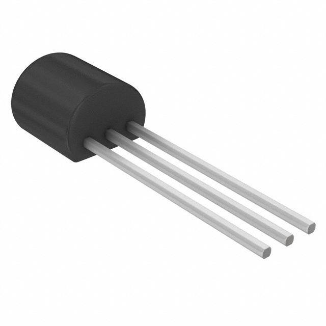
| 描述 | TRANS NPN 400V 2A TO-92 |
| 产品分类 | 晶体管(BJT) - 单路 |
| 品牌 | STMicroelectronics |
| 数据手册 | |
| 产品图片 |
|
| 产品型号 | STX13004G |
| rohs | 无铅 / 符合限制有害物质指令(RoHS)规范要求 |
| 产品系列 | - |
| 不同 Ib、Ic时的 Vce饱和值(最大值) | 1V @ 500mA,2A |
| 不同 Ic、Vce 时的DC电流增益(hFE)(最小值) | 10 @ 1A,5V |
| 产品目录页面 | |
| 供应商器件封装 | TO-92 |
| 其它名称 | 497-8904-5 |
| 其它有关文件 | http://www.st.com/web/catalog/sense_power/FM100/CL822/SC1229/PF222357?referrer=70071840 |
| 功率-最大值 | 2.5W |
| 包装 | 管件 |
| 安装类型 | 通孔 |
| 封装/外壳 | TO-226-3、TO-92-3 标准主体 |
| 晶体管类型 | NPN |
| 标准包装 | 2,500 |
| 电压-集射极击穿(最大值) | 400V |
| 电流-集电极(Ic)(最大值) | 2A |
| 电流-集电极截止(最大值) | 1mA |
| 频率-跃迁 | - |
,TO-226_straightlead.jpg)


- 商务部:美国ITC正式对集成电路等产品启动337调查
- 曝三星4nm工艺存在良率问题 高通将骁龙8 Gen1或转产台积电
- 太阳诱电将投资9.5亿元在常州建新厂生产MLCC 预计2023年完工
- 英特尔发布欧洲新工厂建设计划 深化IDM 2.0 战略
- 台积电先进制程称霸业界 有大客户加持明年业绩稳了
- 达到5530亿美元!SIA预计今年全球半导体销售额将创下新高
- 英特尔拟将自动驾驶子公司Mobileye上市 估值或超500亿美元
- 三星加码芯片和SET,合并消费电子和移动部门,撤换高东真等 CEO
- 三星电子宣布重大人事变动 还合并消费电子和移动部门
- 海关总署:前11个月进口集成电路产品价值2.52万亿元 增长14.8%


PDF Datasheet 数据手册内容提取
STX13004 High voltage fast-switching NPN power transistor Features ■ High voltage capability ■ Low spread of dynamic parameters ) s ■ Minimum lot-to-lot spread for reliable operation ( t ■ Very high switching speed c u d Application o r P ■ SMPS for battery charger e TO-92 TO-92AP t Description e l o The device is manufactured using high voltage s b multi epitaxial planar technology for high switching O Figure 1. Internal schematic diagram speeds and high voltage capability. It uses a cellular emitter structure with planar edge - ) termination to enhance switching speeds swhile maintaining the wide RBSOA. ( t c u d o r P e t e l o s b O Table 1. Device summary Order codes Marking Package Packaging STX13004 X13004 TO-92 Bulk STX13004G (1) X13004G TO-92 Bulk STX13004-AP X13004 TO-92AP Ammopack STX13004G-AP (1) X13004G TO-92AP Ammopack 1. The letter "G" in the order code identifies the product as ECOPACK®2 grade. Please see Section3 for details. July 2010 Doc ID 15543 Rev 3 1/11 www.st.com 11
Electrical ratings STX13004 1 Electrical ratings Table 2. Absolute maximum ratings Symbol Parameter Value Unit V Collector-emitter voltage (V = 0) 700 V CES BE V Collector-emitter voltage (I = 0) 400 V CEO B V Collector-base voltage (I = 0, I = 1 A, t < 10 ms) V V EBO C B P (BR)EBO I Collector current 2 A C ) s I Collector peak current (t < 5 ms) 4 A CM P ( t I Base current 1 c A B u I Base peak current (t < 5 ms) d2 A BM P o P Total dissipation at T = 25 °C r 2.5 W TOT c P T Storage temperature -65 to 150 STG e °C TJ Max. operating junction temperature e t 150 l o s b Table 3. Thermal data O Symbol Pa-rameter Value Unit ) R Thermal resistances junction-case max 50 °C/W thJC ( t R Thermal rescistance junction-ambient max 150 °C/W thJA u d o r P e t e l o s b O 2/11 Doc ID 15543 Rev 3
STX13004 Electrical characteristics 2 Electrical characteristics T = 25 °C; unless otherwise specified. case Table 4. Electrical characteristics Symbol Parameter Test conditions Min. Typ. Max. Unit Collector cut-off current I V = 700 V 10 µA CES (V = 0) CE BE Collector cut-off current ICEO (IB = 0) VCE = 400 V 1s )mA ( Emitter-base breakdown t V I = 10 mA 9 c 18 V (BR)EBO voltage (IC = 0) E u d Collector-emitter sustaining V (1) I = 10 mA o400 V CEO(sus) voltage (IB = 0) C r P VCE(sat) (1) Cvooltllaegcetor-emitter saturation IIC == 12 AA IIBe == 250000 mmAA 01.5 VV C tB e V (1) Base-emitter saturation IC = 1 A o l IB = 200 mA 1.2 V BE(sat) voltage IC = 2 As IB = 500 mA 1.6 V b OI = 0.5 mA V = 2 V 15 35 C CE I = 400 mA V = 2 V 26 h DC current gain - C CE FE ) IC = 1 A VCE = 5 V 10 30 s ( IC = 2 A VCE = 5 V 6 16 t c Resistivue load IC = 2 A __ _ tp = 30 µs d I = -I = 400 mA t Storage time B(on) B(off) 1.1 µs s o V = 125 V V = -5 V tf P rFall time (sCeCe Figure12) BB(off) 300 ns e I = 1 A V = 300 V t Inductive load C clamp e t Storage time IB(on) = 250 mA VBB(off) = -5 V 2.4 µs ol ts Fall time Csnubber = 1 nF RBB(off) = 0 200 ns s f (see Figure13) b O 1. Pulse test: pulse duration ≤ 300 µs, duty cycle ≤ 2 %. Doc ID 15543 Rev 3 3/11
Electrical characteristics STX13004 2.1 Electrical characteristics (curves) Figure 2. Safe operating area Figure 3. Derating curve ) s ( t c u d o r P Figure 4. DC current gain @VCE = 2 V Figure 5. DC cur rent gain @VCE = 5 V e t e l o s b O - ) s ( t c u d o r P e Figure 6. tCollector-emitter saturation voltage Figure 7. Base-emitter saturation voltage e l o s b O 4/11 Doc ID 15543 Rev 3
STX13004 Electrical characteristics Figure 8. Output characteristics Figure 9. Reverse biased SOA ) s ( t c u Figure 10. Resistive load switching times Figure 11. Inductive load swditching times o r P e t e l o s b O - ) s ( t c u d o r P e t e l o s b O Doc ID 15543 Rev 3 5/11
Electrical characteristics STX13004 2.2 Test circuits Figure 12. Resistive load switching test circuit ) s ( t c u d o r P e t e 1. Fast electronic switch l o 2. Non-inductive resistor s b O Figure 13. Inductive load switch ing test circuit - ) s ( t c u d o r P e t e l o s b O 1. Fast electronic switch 2. Non-inductive resistor 3. Fast recovery rectifier 6/11 Doc ID 15543 Rev 3
STX13004 Package mechanical data 3 Package mechanical data In order to meet environmental requirements, ST offers these devices in different grades of ECOPACK® packages, depending on their level of environmental compliance. ECOPACK® specifications, grade definitions and product status are available at: www.st.com. ECOPACK® is an ST trademark. ) s ( t c u d o r P e t e l o s b O - ) s ( t c u d o r P e t e l o s b O Doc ID 15543 Rev 3 7/11
Package mechanical data STX13004 TO-92 bulk shipment mechanical data mm. DIM. MIN. TYP MAX. A 4.32 4.95 b 0.36 0.51 D 4.45 4.95 ) s ( E 3.30 3.9t4 c u e 2.41 2.67 d o e1 1.14 1.40 r P L 12.70 15.49 e t R 2.16 e 2.41 l o S1 0.92 1.52 s b W 0.41 O 0.56 V - 5o ) s ( t c u d o r P e t e l o s b O 0102782 D 8/11 Doc ID 15543 Rev 3
STX13004 Package mechanical data TO-92 ammopack shipment (suffix”-AP”) mechanical data mm Dim. Min Typ Max A1 4.80 T 3.80 T1 1.60 T2 2.30 d 0.48 ) P0 12.50 12.70 12.90 s ( P2 5.65 6.35 7.0t5 c F1,F2 2.44 2.54 2.94 u F3 4.98 5.08 5.48 d delta H -2.00 2.00 o W 17.50 18.00 19.00 r W0 5.70 6.00 P 6.30 W1 8.50 9.00 9.25 e W2 0.50 t H 18.50 e 20.50 H3 0.5 ol1 1.5 H0 15.50 s 16.00 16.50 H1 b 25.00 D0 3.80 O 4.00 4.20 t 0.90 L - 11.00 I1 3.00 ) s delta P -1.00( 1.00 t c u d o r P e t e l o s b O 0050910S Doc ID 15543 Rev 3 9/11
Revision history STX13004 4 Revision history Table 5. Document revision history Date Revision Changes 01-Apr-2009 1 First release. 21-Apr-2010 2 Updated h specification Table4 on page3. FE Added R value Table3 on page2 and updated I maximum 06-Jul-2010 3 thJA CES value Table4 on page3. ) s ( t c u d o r P e t e l o s b O - ) s ( t c u d o r P e t e l o s b O 10/11 Doc ID 15543 Rev 3
STX13004 ) s Please Read Carefully: ( t c u Information in this document is provided solely in connection with ST products. STMicroelectronics NV and its subdsidiaries (“ST”) reserve the right to make changes, corrections, modifications or improvements, to this document, and the products and soervices described herein at any time, without notice. r P All ST products are sold pursuant to ST’s terms and conditions of sale. e Purchasers are solely responsible for the choice, selection and use of the ST products and services described herein, and ST assumes no t liability whatsoever relating to the choice, selection or use of the ST products and servicees described herein. l No license, express or implied, by estoppel or otherwise, to any intellectual propertoy rights is granted under this document. If any part of this document refers to any third party products or services it shall not be deemed sa license grant by ST for the use of such third party products or services, or any intellectual property contained therein or considered asb a warranty covering the use in any manner whatsoever of such third party products or services or any intellectual property contained tOherein. - UNLESS OTHERWISE SET FORTH IN ST’S TERMS )AND CONDITIONS OF SALE ST DISCLAIMS ANY EXPRESS OR IMPLIED s WARRANTY WITH RESPECT TO THE USE AND/OR SALE OF ST PRODUCTS INCLUDING WITHOUT LIMITATION IMPLIED ( WARRANTIES OF MERCHANTABILITY, FITNEtSS FOR A PARTICULAR PURPOSE (AND THEIR EQUIVALENTS UNDER THE LAWS c OF ANY JURISDICTION), OR INFRINGEMENT OF ANY PATENT, COPYRIGHT OR OTHER INTELLECTUAL PROPERTY RIGHT. u UNLESS EXPRESSLY APPROVED dIN WRITING BY AN AUTHORIZED ST REPRESENTATIVE, ST PRODUCTS ARE NOT RECOMMENDED, AUTHORIZED OoR WARRANTED FOR USE IN MILITARY, AIR CRAFT, SPACE, LIFE SAVING, OR LIFE SUSTAINING APPLICATIONS, NOR IN PROrDUCTS OR SYSTEMS WHERE FAILURE OR MALFUNCTION MAY RESULT IN PERSONAL INJURY, P DEATH, OR SEVERE PROPERTY OR ENVIRONMENTAL DAMAGE. ST PRODUCTS WHICH ARE NOT SPECIFIED AS "AUTOMOTIVE GRADE" MAY ONLYe BE USED IN AUTOMOTIVE APPLICATIONS AT USER’S OWN RISK. t e l Resale of oST products with provisions different from the statements and/or technical features set forth in this document shall immediately void any wsarranty granted by ST for the ST product or service described herein and shall not create or extend in any manner whatsoever, any liabbility of ST. O ST and the ST logo are trademarks or registered trademarks of ST in various countries. Information in this document supersedes and replaces all information previously supplied. The ST logo is a registered trademark of STMicroelectronics. All other names are the property of their respective owners. © 2010 STMicroelectronics - All rights reserved STMicroelectronics group of companies Australia - Belgium - Brazil - Canada - China - Czech Republic - Finland - France - Germany - Hong Kong - India - Israel - Italy - Japan - Malaysia - Malta - Morocco - Philippines - Singapore - Spain - Sweden - Switzerland - United Kingdom - United States of America www.st.com Doc ID 15543 Rev 3 11/11