ICGOO在线商城 > 分立半导体产品 > 二极管 - 整流器 - 单 > STTH3R02QRL
 Datasheet下载
- 型号: STTH3R02QRL
- 制造商: STMicroelectronics
- 库位|库存: xxxx|xxxx
- 要求:
| 数量阶梯 | 香港交货 | 国内含税 |
| +xxxx | $xxxx | ¥xxxx |
查看当月历史价格
查看今年历史价格
STTH3R02QRL产品简介:
ICGOO电子元器件商城为您提供STTH3R02QRL由STMicroelectronics设计生产,在icgoo商城现货销售,并且可以通过原厂、代理商等渠道进行代购。 STTH3R02QRL价格参考¥1.47-¥1.47。STMicroelectronicsSTTH3R02QRL封装/规格:二极管 - 整流器 - 单, 标准 通孔 二极管 200V 3A DO-15。您可以下载STTH3R02QRL参考资料、Datasheet数据手册功能说明书,资料中有STTH3R02QRL 详细功能的应用电路图电压和使用方法及教程。
STMicroelectronics 的 STTH3R02QRL 是一款高效、低正向电压降(Vf)的整流二极管,属于 STPOWER 系列,主要应用于需要高效率和低功耗的场景。以下是其典型应用场景:

 1. 开关电源 (SMPS)
   - 该型号适用于开关电源中的次级整流部分,能够有效降低导通损耗,提高整体转换效率。
   - 常用于 AC-DC 或 DC-DC 转换器中,支持高频整流需求。

 2. 适配器与充电器
   - 在手机、笔记本电脑或其他电子设备的适配器和充电器中,作为输出整流二极管,提供稳定的直流输出。
   - 其低 Vf 特性有助于减少发热,延长产品寿命。

 3. 太阳能逆变器
   - 在光伏系统中,可用于最大功率点跟踪(MPPT)控制器或逆变器的整流电路,确保能量高效传输。
   - 支持可再生能源系统的节能需求。

 4. 电机驱动与控制
   - 应用于家用电器(如冰箱、空调、洗衣机等)的电机驱动电路中,进行电流整流。
   - 适合需要高可靠性和低功耗的家电设计。

 5. 工业自动化
   - 在工业控制系统中,用于信号隔离、保护电路或电源整流。
   - 具备良好的热性能和电气特性,适应恶劣的工作环境。

 6. 汽车电子
   - 可用于车载充电器、LED 照明驱动或辅助电源模块中。
   - 满足汽车级应用对稳定性和可靠性的要求。

 7. 电池管理
   - 在电池管理系统中,用于防止反向电流流动,保护电池组免受损坏。
   - 适用于电动工具、无人机和其他便携式设备。

 总结
STTH3R02QRL 凭借其低正向压降、高浪涌能力和紧凑封装,广泛应用于消费电子、工业设备、汽车电子和可再生能源领域。它特别适合需要高效整流和低功耗的设计场景,能够显著提升系统的性能和可靠性。
| 参数 | 数值 |
| 产品目录 | |
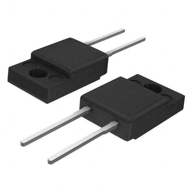
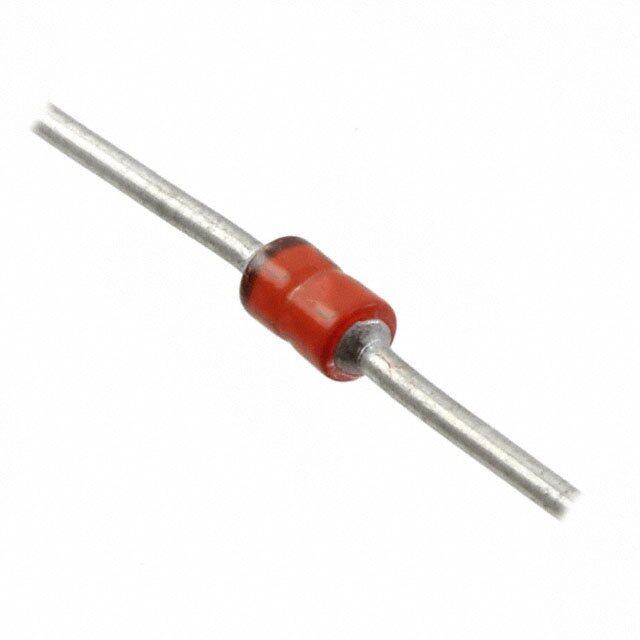
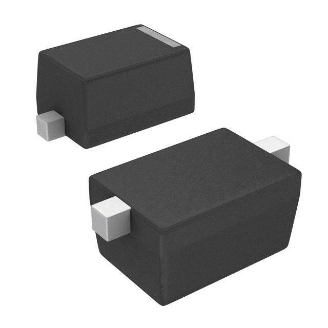
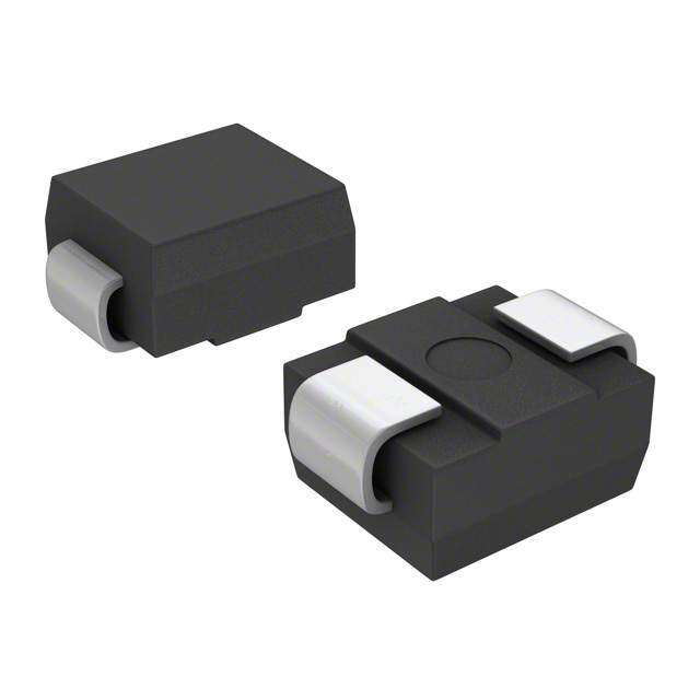
| 描述 | DIODE ULTRA FAST 200V 3A DO15整流器 high voltage diode |
| 产品分类 | 单二极管/整流器分离式半导体 |
| 品牌 | STMicroelectronics |
| 产品手册 | |
| 产品图片 |
|
| rohs | 符合RoHS无铅 / 符合限制有害物质指令(RoHS)规范要求 |
| 产品系列 | 二极管与整流器,整流器,STMicroelectronics STTH3R02QRL- |
| 数据手册 | |
| 产品型号 | STTH3R02QRL |
| 不同If时的电压-正向(Vf) | 1V @ 3A |
| 不同 Vr、F时的电容 | - |
| 不同 Vr时的电流-反向漏电流 | 3µA @ 200V |
| 二极管类型 | 标准 |
| 产品 | Ultra Fast Recovery Rectifiers |
| 产品目录页面 | |
| 产品种类 | 整流器 |
| 供应商器件封装 | DO-15 |
| 其它名称 | 497-5765-1 |
| 其它有关文件 | http://www.st.com/web/catalog/sense_power/FM64/CL830/SC4/SS1648/PF134620?referrer=70071840 |
| 包装 | 剪切带 (CT) |
| 反向恢复时间(trr) | 30ns |
| 反向电压 | 200 V |
| 反向电流IR | 3 uA |
| 商标 | STMicroelectronics |
| 安装类型 | 通孔 |
| 安装风格 | Through Hole |
| 封装 | Reel |
| 封装/外壳 | DO-204AC,DO-15,轴向 |
| 封装/箱体 | DO-15 |
| 工作温度-结 | 175°C (最大) |
| 工厂包装数量 | 6000 |
| 恢复时间 | 30 ns |
| 最大工作温度 | + 175 C |
| 最大浪涌电流 | 75 A |
| 最小工作温度 | - 65 C |
| 标准包装 | 1 |
| 正向电压下降 | 1.2 V at 9 A |
| 正向连续电流 | 3 A |
| 热阻 | 45°C/W Jl |
| 电压-DC反向(Vr)(最大值) | 200V |
| 电流-平均整流(Io) | 3A |
| 系列 | STTH3R02 |
| 速度 | 快速恢复 =< 500 ns,> 200mA(Io) |
| 配置 | Single |


- 商务部:美国ITC正式对集成电路等产品启动337调查
- 曝三星4nm工艺存在良率问题 高通将骁龙8 Gen1或转产台积电
- 太阳诱电将投资9.5亿元在常州建新厂生产MLCC 预计2023年完工
- 英特尔发布欧洲新工厂建设计划 深化IDM 2.0 战略
- 台积电先进制程称霸业界 有大客户加持明年业绩稳了
- 达到5530亿美元!SIA预计今年全球半导体销售额将创下新高
- 英特尔拟将自动驾驶子公司Mobileye上市 估值或超500亿美元
- 三星加码芯片和SET,合并消费电子和移动部门,撤换高东真等 CEO
- 三星电子宣布重大人事变动 还合并消费电子和移动部门
- 海关总署:前11个月进口集成电路产品价值2.52万亿元 增长14.8%


PDF Datasheet 数据手册内容提取
STTH3R02 Ultrafast recovery diode Datasheet - production data Table 1. Device summary A K I 3 A F(AV) V 200 V RRM T (max) 175 °C j AA AA V (typ) 0.7 V F KK DO-201AD KK DO-15 trr (typ) 16 ns STTH3R02 STTH3R02Q A K SMC STTH3R02S Features • Very low conduction losses • Negligible switching losses • Low forward and reverse recovery times • High junction temperature Description The STTH3R02 uses ST's new 200 V planar Pt doping technology, and it is specially suited for switching mode base drive and transistor circuits. Packaged in DO-201AD, DO-15, and SMC, this device is intended for use in low voltage, high frequency inverters, free wheeling and polarity protection. April 2014 DocID12359 Rev 3 1/9 This is information on a product in full production. www.st.com
Characteristics STTH3R02 1 Characteristics Table 2. Absolute ratings (limiting values at T = 25 °C, unless otherwise specified) j Symbol Parameter Value Unit V Repetitive peak reverse voltage 200 V RRM IFRM Repetitive peak forward current tp = 5 µs, F = 5 kHz 110 A DO-201AD / DO-15 70 I Forward rms current A F(RMS) SMC 70 DO-15 T = 50 °C lead I Average forward current, δ = 0.5 DO-201AD T = 90 °C 3 A F(AV) lead SMC T = 110 °C c I Surge non repetitive forward current t = 10 ms Sinusoidal 75 A FSM p T Storage temperature range -65 to + 175 °C stg T Maximum operating junction temperature 175 °C j Maximum lead temperature for soldering during 10 s at 4 mm from T 230 °C L case Table 3. Thermal parameters Symbol Parameter Value Unit Lead Length = 10 mm on infinite DO-15 45 R Junction to lead th(j-l) heatsink DO-201AD 30 °C/W R Junction to case SMC 20 th(j-c) Table 4. Static electrical characteristics Symbol Parameter Test conditions Min. Typ. Max. Unit I (1) Reverse leakage Tj = 25 °C V = V 3 µA R current T = 125 °C R RRM 3 30 j T = 25 °C I = 9 A 1.20 j F T = 25 °C 0.89 1.0 V (2) Forward voltage drop j V F T = 100 °C I = 3 A 0.76 0.85 j F T = 150 °C 0.70 0.80 j 1. Pulse test: t = 5 ms, δ < 2 % p 2. Pulse test: t = 380 µs, δ < 2 % p To evaluate the conduction losses use the following equation: P = 0.68 x I + 0.04 I 2 F(AV) F (RMS) 2/9 DocID12359 Rev 3
STTH3R02 Characteristics Table 5. Dynamic characteristics Symbol Parameter Test conditions Min. Typ. Max. Unit I = 1 A, dI /dt = -50 A/µs, F F 24 30 V = 30 V, T = 25 °C R j t Reverse recovery time ns rr I = 1 A, dI /dt = -100 A/µs, F F 16 20 V = 30 V, T = 25 °C R j I = 3 A, dI /dt = -200 A/µs, I Reverse recovery current F F 3.5 4.5 A RM V = 160 V, T = 125 °C R j I = 3 A, dI /dt = 100 A/µs t Forward recovery time F F 40 ns fr V = 1.1 x V , T = 25 °C FR Fmax j I = 3 A, dI /dt = 100 A/µs, F F V Forward recovery voltage 1.9 V FP T = 25 °C j Figure 1 . peak current versus duty cycle Figure 2. Forward voltage drop versus forward current (typical values) IM(A) 100 IFM(A) TT 50 IIMM 80 dδ==ttpp//TT ttpp 40 60 30 PP == 1100WW 40 20 PP == 55WW PP == 33WW 20 10 Tj=150°C δ Tj=25°C VFM(V) 0 0 0.0 0.1 0.2 0.3 0.4 0.5 0.6 0.7 0.8 0.9 1.0 0.0 0.5 1.0 1.5 2.0 Figure 3. Fo r ward voltage drop versus forward Figure 4. Relative variation of thermal current (maximum values) impedance junction to ambient versus pulse duration - DO-201AD 50 IFM(A) 1.0 Zth(j-a)/Rth(j-a) 0.9 Epoxy printed circuit board FR4,eCU= 35 µm 40 0.8 LDleOad-s2=0110A mDm 0.7 30 0.6 0.5 20 0.4 Tj=150°C 0.3 10 Tj=25°C 0.2 Single pulse VFM(V) 0.1 tP(s) 0 0.0 0.0 0.5 1.0 1.5 2.0 1.E-01 1.E+00 1.E+01 1.E+02 1.E+03 DocID12359 Rev 3 3/9 9
Characteristics STTH3R02 Figure 5 . Relative variation of thermal Figure 6. Relative variation of thermal impedance junction to ambient versus pulse impedance junction to ambient versus pulse duration - DO-15 duration - SMC 1.0 Zth(j-a)/Rth(j(-ja-a)) 1.0 Zth(j-a)/Rth(j-a) 0.9 Epoxy printed circuit board FR4,eCU= 35 µm 0.9 Epoxy printed circuit board FR4,eCU= 35 µm 0.8 LleaDdsO=1-105 mm 0.8 SMC 0.7 0.7 Scu=1 cm² 0.6 0.6 0.5 0.5 0.4 0.4 0.3 0.3 0.2 0.2 0.1 Single pulse 0.1 Single pulse 0.0 tP(s) 0.0 tP(s) 1.E-01 1.E+00 1.E+01 1.E+02 1.E+03 1.E-03 1.E-02 1.E-01 1.E+00 1.E+01 1.E+02 1.E+03 Figure 7. Ju n ction capacitance versus reverse Figure 8. Reverse recovery charges versus applied voltage (typical values) dI /dt (typical values) F 100 C(pF) 80 QRR(nC) VosFcT==j=3120M5m°HVCzRMS 70 VRIF==136A0V 60 50 10 40 Tj=125°C 30 20 Tj=25°C 10 VR(V) dIF/dt(A/µs) 1 0 1 10 100 1000 10 100 1000 Figure 9. R e verse recovery time versus dI /dt Figure 10. Peak reverse recovery current F (typical values) versus dI /dt (typical values) F tRR(ns) IRM(A) 60 8 VRIF==136A0V 7 VRIF==136A0V 50 6 40 5 Tj=125°C 30 4 Tj=125°C 20 Tj=25°C 3 2 10 1 Tj=25°C dIF/dt(A/µs) dIF/dt(A/µs) 0 0 10 100 1000 10 100 1000 4/9 DocID12359 Rev 3
STTH3R02 Ordering information scheme Figure 11. D y namic parameters versus junction Figure 12. Thermal resistance junction to temperature ambient versus copper surface under each lead QRR;IRM[Tj]/QRR;IRM[Tj=125°C] Rth(j-a)(°C/W) 1.4 100 1.2 VRIF==136A0V 90 Epoxy printed circuit board FR4,eCU= 35 µm 80 1.0 70 0.8 IRM 60 DO-15 50 0.6 DO-201AD QRR 40 0.4 30 20 0.2 0.0 Tj(°C) 100 SCu(cm²) 25 50 75 100 125 150 0.0 0.5 1.0 1.5 2.0 2.5 3.0 3.5 4.0 4.5 5.0 Figure 13. T hermal resistance versus copper Figure 14. Thermal resistance versus lead surface under each lead for SMC length for DO-201AD package 100 Rth(j-a)(°C/W) 100 Rth(°C/W) Epoxy printed circuit board FR4,eCU= 35 µm SMC 90 DO-201AD 80 80 Rth(j-a) 70 60 60 50 40 40 Rth(j-l) 30 20 20 SCU(cm²) 10 Lleads(mm) 0 0 0.0 0.5 1.0 1.5 2.0 2.5 3.0 3.5 4.0 4.5 5.0 5 10 15 20 25 2 Ordering information scheme Figure 15. Ordering information scheme STTH 3 R 02 XXX Ultrafast switching diode Average forward current 3 = 3 A Model R Repetitive peak reverse voltage 02 = 200V Package Blank = DO-201 in Ammopack RL = DO-201 inTape and reel Q = DO-15 in Ammopack QRL = DO-15 inTape and reel S= SMC inTape and reel DocID12359 Rev 3 5/9 9
Package information STTH3R02 3 Package information • Epoxy meets UL94, V0 • Cooling method: by conduction (C) In order to meet environmental requirements, ST offers these devices in different grades of ECOPACK® packages, depending on their level of environmental compliance. ECOPACK® specifications, grade definitions and product status are available at: www.st.com. ECOPACK® is an ST trademark. Table 6. DO-201AD dimensions Dimensions Ref. Millimeters Inches Min. Max. Min. Max. B A B A 9.50 0.374 Note 1 E E Note 1 B 25.40 1.000 ØD Note 2 C 5.30 0.209 ØC D 1.30 0.051 E 1.25 0.049 1 - The lead diameter ø D is not controlled over zone E Notes 2 - The minimum length which must stay straight between the right angles after bending is 0.59"(15mm) Table 7. DO-15 dimensions Dimensions C A C Ref. Millimeters Inches Min. Max. Min. Max. A 6.05 6.75 0.238 0.266 B 2.95 3.53 0.116 0.139 D B C 26 31 1.024 1.220 D 0.71 0.88 0.028 0.035 6/9 DocID12359 Rev 3
STTH3R02 Package information Table 8. SMC dimensions Dimensions Ref. Millimeters Inches E1 Min. Max. Min. Max. A1 1.90 2.45 0.075 0.096 D A2 0.05 0.20 0.002 0.008 b 2.90 3.2 0.114 0.126 c 0.15 0.41 0.006 0.016 E E 7.75 8.15 0.305 0.321 A1 E1 6.60 7.15 0.260 0.281 C A2 E2 4.40 4.70 0.173 0.185 E2 L b D 5.55 6.25 0.218 0.246 L 0.75 1.60 0.030 0.063 Figure 16. SMC footprint (dimensions in mm) 2.20 4.25 2.20 3.30 8.65 DocID12359 Rev 3 7/9 9
Ordering information STTH3R02 4 Ordering information Table 9. Ordering information Order code Marking Package Weight Base qty Delivery mode STTH3R02 STTH3R02 DO-201AD 1.16 g 600 Ammopack STTH3R02RL STTH3R02 DO-201AD 1.16 g 1900 Tape and reel STTH3R02Q STTH3R02 DO-15 0.4 g 1000 Ammopack STTH3R02QRL STTH3R02 DO-15 0.4 g 6000 Tape and reel STTH3R02S 3R2S SMC 0.243 g 2500 Tape and reel 5 Revision history Table 10. Document revision history Date Revision Changes 03-May-2006 1 First issue. 10-Oct-2006 2 Added SMC package. 17-Apr-2014 3 Updated ECOPACK statement. Reformatted to current standards. 8/9 DocID12359 Rev 3
STTH3R02 Please Read Carefully: Information in this document is provided solely in connection with ST products. STMicroelectronics NV and its subsidiaries (“ST”) reserve the right to make changes, corrections, modifications or improvements, to this document, and the products and services described herein at any time, without notice. All ST products are sold pursuant to ST’s terms and conditions of sale. Purchasers are solely responsible for the choice, selection and use of the ST products and services described herein, and ST assumes no liability whatsoever relating to the choice, selection or use of the ST products and services described herein. No license, express or implied, by estoppel or otherwise, to any intellectual property rights is granted under this document. If any part of this document refers to any third party products or services it shall not be deemed a license grant by ST for the use of such third party products or services, or any intellectual property contained therein or considered as a warranty covering the use in any manner whatsoever of such third party products or services or any intellectual property contained therein. UNLESS OTHERWISE SET FORTH IN ST’S TERMS AND CONDITIONS OF SALE ST DISCLAIMS ANY EXPRESS OR IMPLIED WARRANTY WITH RESPECT TO THE USE AND/OR SALE OF ST PRODUCTS INCLUDING WITHOUT LIMITATION IMPLIED WARRANTIES OF MERCHANTABILITY, FITNESS FOR A PARTICULAR PURPOSE (AND THEIR EQUIVALENTS UNDER THE LAWS OF ANY JURISDICTION), OR INFRINGEMENT OF ANY PATENT, COPYRIGHT OR OTHER INTELLECTUAL PROPERTY RIGHT. ST PRODUCTS ARE NOT DESIGNED OR AUTHORIZED FOR USE IN: (A) SAFETY CRITICAL APPLICATIONS SUCH AS LIFE SUPPORTING, ACTIVE IMPLANTED DEVICES OR SYSTEMS WITH PRODUCT FUNCTIONAL SAFETY REQUIREMENTS; (B) AERONAUTIC APPLICATIONS; (C) AUTOMOTIVE APPLICATIONS OR ENVIRONMENTS, AND/OR (D) AEROSPACE APPLICATIONS OR ENVIRONMENTS. WHERE ST PRODUCTS ARE NOT DESIGNED FOR SUCH USE, THE PURCHASER SHALL USE PRODUCTS AT PURCHASER’S SOLE RISK, EVEN IF ST HAS BEEN INFORMED IN WRITING OF SUCH USAGE, UNLESS A PRODUCT IS EXPRESSLY DESIGNATED BY ST AS BEING INTENDED FOR “AUTOMOTIVE, AUTOMOTIVE SAFETY OR MEDICAL” INDUSTRY DOMAINS ACCORDING TO ST PRODUCT DESIGN SPECIFICATIONS. PRODUCTS FORMALLY ESCC, QML OR JAN QUALIFIED ARE DEEMED SUITABLE FOR USE IN AEROSPACE BY THE CORRESPONDING GOVERNMENTAL AGENCY. Resale of ST products with provisions different from the statements and/or technical features set forth in this document shall immediately void any warranty granted by ST for the ST product or service described herein and shall not create or extend in any manner whatsoever, any liability of ST. ST and the ST logo are trademarks or registered trademarks of ST in various countries. Information in this document supersedes and replaces all information previously supplied. The ST logo is a registered trademark of STMicroelectronics. All other names are the property of their respective owners. © 2014 STMicroelectronics - All rights reserved STMicroelectronics group of companies Australia - Belgium - Brazil - Canada - China - Czech Republic - Finland - France - Germany - Hong Kong - India - Israel - Italy - Japan - Malaysia - Malta - Morocco - Philippines - Singapore - Spain - Sweden - Switzerland - United Kingdom - United States of America www.st.com DocID12359 Rev 3 9/9 9
Mouser Electronics Authorized Distributor Click to View Pricing, Inventory, Delivery & Lifecycle Information: S TMicroelectronics: STTH3R02QRL STTH3R02 STTH3R02RL STTH3R02S STTH3R02Q