ICGOO在线商城 > STP16DPP05TTR

 Datasheet下载
- 型号: STP16DPP05TTR
- 制造商: STMicroelectronics
- 库位|库存: xxxx|xxxx
- 要求:
| 数量阶梯 | 香港交货 | 国内含税 |
| +xxxx | $xxxx | ¥xxxx |
查看当月历史价格
查看今年历史价格
STP16DPP05TTR产品简介:
ICGOO电子元器件商城为您提供STP16DPP05TTR由STMicroelectronics设计生产,在icgoo商城现货销售,并且可以通过原厂、代理商等渠道进行代购。 提供STP16DPP05TTR价格参考以及STMicroelectronicsSTP16DPP05TTR封装/规格参数等产品信息。 你可以下载STP16DPP05TTR参考资料、Datasheet数据手册功能说明书, 资料中有STP16DPP05TTR详细功能的应用电路图电压和使用方法及教程。
| 参数 | 数值 |
| 产品目录 | 集成电路 (IC) |
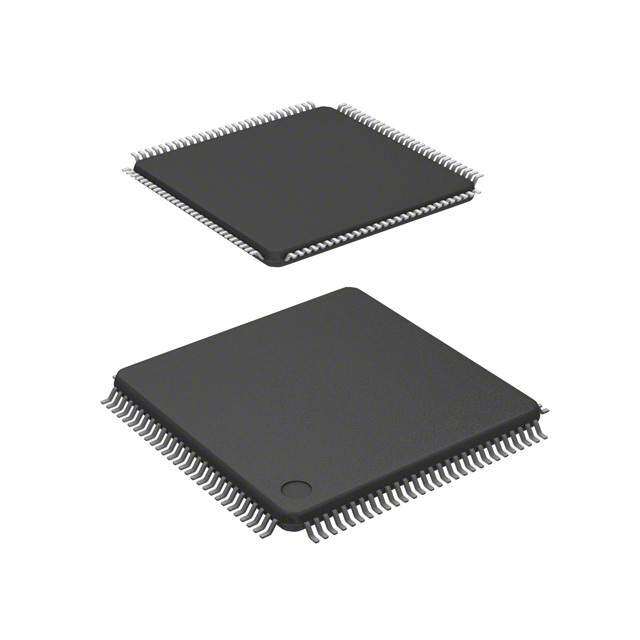
| 描述 | IC LED DRIVER LINEAR 24TSSOP |
| 产品分类 | |
| 品牌 | STMicroelectronics |
| 数据手册 | |
| 产品图片 |
|
| 产品型号 | STP16DPP05TTR |
| rohs | 无铅 / 符合限制有害物质指令(RoHS)规范要求 |
| 产品系列 | - |
| 产品目录页面 | |
| 供应商器件封装 | 24-TSSOP |
| 其它名称 | 497-10322-1 |
| 其它有关文件 | http://www.st.com/web/catalog/sense_power/FM142/CL1854/SC1573/PF222890?referrer=70071840 |
| 内部驱动器 | 是 |
| 包装 | 剪切带 (CT) |
| 安装类型 | 表面贴装 |
| 封装/外壳 | 24-TSSOP(0.173",4.40mm 宽) |
| 工作温度 | -40°C ~ 125°C |
| 恒压 | - |
| 恒流 | 是 |
| 拓扑 | 线性,高端 |
| 标准包装 | 1 |
| 电压-电源 | 3 V ~ 5.5 V |
| 电压-输出 | 20V |
| 类型-初级 | 通用 |
| 类型-次级 | - |
| 输出数 | 16 |
| 频率 | 30MHz |


- 商务部:美国ITC正式对集成电路等产品启动337调查
- 曝三星4nm工艺存在良率问题 高通将骁龙8 Gen1或转产台积电
- 太阳诱电将投资9.5亿元在常州建新厂生产MLCC 预计2023年完工
- 英特尔发布欧洲新工厂建设计划 深化IDM 2.0 战略
- 台积电先进制程称霸业界 有大客户加持明年业绩稳了
- 达到5530亿美元!SIA预计今年全球半导体销售额将创下新高
- 英特尔拟将自动驾驶子公司Mobileye上市 估值或超500亿美元
- 三星加码芯片和SET,合并消费电子和移动部门,撤换高东真等 CEO
- 三星电子宣布重大人事变动 还合并消费电子和移动部门
- 海关总署:前11个月进口集成电路产品价值2.52万亿元 增长14.8%

PDF Datasheet 数据手册内容提取
STP16DPP05 Low voltage 16-bit constant current LED sink driver with output error detection Datasheet - production data feeds a 16- bit D-type storage register. In the output stage, sixteen regulated current sources are designed to provide 3 to 40 mA of constant current to drive the LEDs. The STP16DPP05 features open and short LED detection on the outputs. The detection circuit checks for 3 different conditions that can occur on the output line: short to GND, short to V or open line. The O data detection results are loaded in the shift registers and shifted out via the serial line output. The detection functionality is implemented without increasing the pin count, through a secondary function of the output enable and latch pin (DM1 and DM2 respectively). A dedicated Features logic sequence allows the device to enter or exit from detection mode. The STP16DPP05 output Low voltage power supply down to 3 V current can be adjusted through an external 16 constant current output channels resistor to control the light intensity of the LEDs. Adjustable output current through external LED brightness is adjustable from 0% to 100% resistor Short and open output error detection via the OE/DM2 pin. The STP16DPP05 Serial data IN/parallel data OUT guarantees a 20 V output driving capability, 3.3 V MCU-driving capability allowing users to connect more LEDs in series. Output current: 3 to 40 mA The high 30 MHz clock frequency makes the 30 MHz clock frequency device suitable for high data rate transmission. Available in high thermal efficiency TSSOP The 3.3 V supply is well suited for applications exposed pad which interface a 3.3 V MCU. Compared to a ESD protection: 2 kV HBM, 200 V MM standard TSSOP package, the TSSOP with exposed pad increases heat dissipation capability Description by a factor of 2.5. The STP16DPP05 is a monolithic, low voltage, low current power 16-bit shift register designed for LED panel displays. The device features a 16-bit serial-in, parallel-out shift register that Table 1: Device summary Order code Package Packing STP16DPP05MTR SO-24 (tape and reel) 1000 parts per reel STP16DPP05TTR TSSOP24 (tape and reel) 2500 parts per reel STP16DPP05XTTR TSSOP24 exposed pad (tape and reel) 2500 parts per reel STP16DPP05PTR QSOP-24 2500 parts per reel April 2017 DocID16518 Rev 4 1/34 This is information on a product in full production. www.st.com
Contents STP16DPP05 Contents 1 Summary description ...................................................................... 3 1.1 Pin connection and description ......................................................... 3 2 Electrical ratings ............................................................................. 4 2.1 Absolute maximum ratings ................................................................ 4 2.2 Thermal data ..................................................................................... 4 2.3 Recommended operating conditions ................................................. 5 3 Electrical characteristics ................................................................ 6 4 Equivalent circuit and outputs ....................................................... 8 5 Timing diagrams ............................................................................ 11 6 Typical characteristics .................................................................. 14 7 Error detection mode functionality .............................................. 18 7.1 Phase one: entering error detection mode ...................................... 18 7.2 Phase two: error detection .............................................................. 19 7.3 Phase three: resuming normal mode .............................................. 21 7.4 Error detection conditions ............................................................... 21 8 Package information ..................................................................... 23 8.1 QSOP-24 package information ....................................................... 24 8.2 SO-24 package information ............................................................ 26 8.3 TSSOP24 package information ....................................................... 27 8.4 TSSOP exposed pad package information ..................................... 29 8.5 TSSOP24, TSSOP24 exposed pad and ............................................. SO-24 packing information .............................................................. 31 9 Revision history ............................................................................ 33 2/34 DocID16518 Rev 4
STP16DPP05 Summary description 1 Summary description Table 2: Typical current accuracy Current accuracy Output voltage Output current VDD Temperature Between bits Between ICs ≥ 1.3 V ± 1% ± 2% 5 to 40 mA 3.3 V to 5 V 25 °C 1.1 Pin connection and description Figure 1: Pin connection The exposed pad should be electrically connected to a metal land electrically isolated or connected to ground. Table 3: Pin description Pin n° Symbol Name and function 1 GND Ground terminal 2 SDI Serial data input terminal 3 CLK Clock input terminal 4 LE/DM1 Latch input terminal - detect mode 1 (see operation principle) 5-20 OUT 0-15 Output terminal Input terminal of output enable (active low) - detect mode 1 21 OE/DM2 (see operation principle) 22 SDO Serial data out terminal 23 R-EXT Input terminal for an external resistor for constant current programming 24 VDD Supply voltage terminal DocID16518 Rev 4 3/34
Electrical ratings STP16DPP05 2 Electrical ratings 2.1 Absolute maximum ratings Stressing the device above the ratings listed in the “absolute maximum ratings” table may cause permanent damage to the device. These are stress ratings only and operation of the device at these or any other condition above those indicated in the operating sections of this specification is not implied. Exposure to absolute maximum rating conditions for extended periods may affect device reliability. Table 4: Absolute maximum ratings Symbol Parameter Value Unit VDD Supply voltage 0 to 7 V VO Output voltage -0.5 to 20 V IO Output current 50 mA VI Input voltage -0.4 to VDD V IGND GND terminal current 800 mA fCLK Clock frequency 50 MHz TJ Junction temperature range (1) -40 to +170 °C Notes: (1) Such absolute value is based on the thermal shutdown protection. 2.2 Thermal data Table 5: Thermal data Symbol Parameter Value Unit TA Operating free-air temperature range -40 to +125 °C TJ-OPR Operating thermal junction temperature range -40 to +150 °C TSTG Storage temperature range -55 to +150 °C SO-24 42.7 °C/W TSSOP24 55 °C/W RthJA Thermal resistance junction-ambient (1) TSSOP24 (2) 37.5 °C/W exposed pad QSOP-24 55 °C/W Notes: (1) According with JEDEC standard 51-7. (2) The exposed pad should be soldered directly to the PCB to obtain the thermal benefits. 4/34 DocID16518 Rev 4
STP16DPP05 Electrical ratings 2.3 Recommended operating conditions Table 6: Recommended operating conditions Symbol Parameter Test conditions Min. Typ. Max. Unit VDD Supply voltage 3 5.5 V VO Output voltage 20 V IO Output current OUTn 3 40 mA IOH Output current SERIAL-OUT 1 mA IOL Output current SERIAL-OUT -1 mA VIH Input voltage 0.7 VDD VDD V VIL Input voltage -0.3 0.3 VDD V twLAT LE/DM1 pulse width 20 ns twCLK CLK pulse width 10 ns twEN OE/DM2 pulse width VDD = 3.0 V to 5.0 V 100 ns tSETUP(D) Setup time for DATA ns tHOLD(D) Hold time for DATA 5 ns tSETUP(L) Setup time for LATCH 8 ns fCLK Clock frequency Cascade operation (1) 30 MHz Notes: (1) If the device is connected in cascade, it may not be possible achieve the maximum data transfer. Please consider the timings carefully. DocID16518 Rev 4 5/34
Electrical characteristics STP16DPP05 3 Electrical characteristics V = 3.3 V to 5 V, T = 25 °C, unless otherwise specified. DD A Table 7: Electrical characteristics Symbol Parameter Test conditions Min. Typ. Max. Unit VIH Input voltage high level 0.7 VDD VDD V VIL Input voltage low level GND 0.3 VDD V IOH Output leakage current VOH = 20 V 1 μA VOL Output voltage (serial-OUT) IOL = 1 mA 0.4 V VOH Output voltage (serial-OUT) IOH = -1 mA VDD-0.4V V IOL1 VO = 0.3 V, Rext = 4 kΩ 4.75 5 5.25 IOL2 Output current VO = 0.3 V, Rext = 1 kΩ 19 20 21 IOL3 VO = 1.3 V, Rext = 497 Ω 38 40 42 mA VO = 0.3 V, IO = 5 mA ΔIOL1 Rext = 4 kΩ ± 1 ± 5 Output current error between VO = 0.3 V, IO = 20 mA ΔIOL2 bit (all output ON) Rext = 980 Ω ± 0.5 ± 3 % VO = 1.3 V, IO = 40 mA ΔIOL3 Rext = 490 Ω ± 0.5 ± 3 RSIN(up) Pull-up resistor 150 300 600 kΩ RSIN(down) Pull-down resistor 100 200 400 kΩ IDD(OFF1) ROeUxtT = 0 1 t ok Ω1,5 I O=U OT =F F2 0 mA, 5.4 7.5 mA Supply current (OFF) IDD(OFF2) ROeUxtT = 0 4 t9o7 1 Ω5 ,= IO OUTF =F 40 mA 8 9.5 IDD(ON1) ROeUxtT = 0 1 t ok Ω1,5 I O=U OT =N 20 mA, 5.5 7.5 Supply current (ON) IDD(ON2) ROeUxtT = 0 4 t9o7 1 Ω5 ,= IO OUTN = 40 mA 8.1 9.5 Thermal Thermal protection 170 °C 6/34 DocID16518 Rev 4
STP16DPP05 Electrical characteristics V = 3.3 V to 5 V, T = 25 °C, unless otherwise specified. DD A Table 8: Switching characteristics Symbol Parameter Test conditions Min. Typ. Max. Unit Propagation delay time, VDD = 3.3 V 35.5 44.5 CLK- OUTn , LE/DM1 = H, tPLH1 OE/DM2 = L VDD = 5 V 18.5 24 ns Propagation delay time, VDD = 3.3 V 41.5 50 LE/DM1 - OUTn , tPLH2 OE/DM2 = L VDD = 5 V 23 29 ns Propagation delay time, VDD = 3.3 V 45 54 tPLH3 OE/DM2 - OUTn , LE = H VDD = 5 V 25 31 ns tPLH PCrLoKp-aSgDaOtio n delay time, VVDDDD == 35. 3V V 1151 2115 3211 ns Propagation delay time, VIH = VDD VDD = 3.3 V 13.7 18 tPHL1 CLK- OUTn , LE/DM1 = H, VIL = GND CL = 10 pF OE/DM2 = L IO = 20 mA VL = 3.0 V VDD = 5 V 8.8 12.5 ns Rext = 1 KΩ RL = 60 Ω Propagation delay time, VDD = 3.3 V 17 22 LE/DM1 - OUTn tPHL2 OE/DM2 = L VDD = 5 V 13 17 ns Propagation delay time, VDD = 3.3 V 12.7 17 tPHL3 OE/DM2 - OUTn , LE/DM1 = H VDD = 5 V 9.5 13 ns tPHL CPLrKop-SaDgaOti on delay time, VVDDDD == 35. 3V V 1172..55 2147 3265 ns tON Ovoulttapguet rwisaev teimfoerm 1 0~90% of VVDDDD == 35. 3V V 2187 3293 ns tOFF Ovoulttapguet fwalal vtiemfoer 9m0 ~10% of VVDDDD == 35. 3V V 43..55 65 ns tr CLK rise time (1) 5000 ns tf CLK fall time (1) 5000 ns Notes: (1) In order to achieve high cascade data transfer, please consider tr/tf timings carefully. DocID16518 Rev 4 7/34
Equivalent circuit and outputs STP16DPP05 4 Equivalent circuit and outputs Figure 2: OE/DM2 terminal Figure 3: LE/DM1 terminal 8/34 DocID16518 Rev 4
STP16DPP05 Equivalent circuit and outputs Figure 4: CLK, SDI terminal Figure 5: SDO terminal DocID16518 Rev 4 9/34
Equivalent circuit and outputs STP16DPP05 Figure 6: Block diagram 10/34 DocID16518 Rev 4
STP16DPP05 Timing diagrams 5 Timing diagrams Table 9: Truth table CLOCK LE/DM1 OE/DM2 SERIAL-IN OUT0 ............. OUT7 ................ OUT15 SDO _|¯ H L Dn Dn ..... Dn - 7 ..... Dn -15 Dn - 15 _|¯ L L Dn + 1 No change Dn - 14 _|¯ H L Dn + 2 Dn + 2 ..... Dn - 5 ..... Dn -13 Dn - 13 ¯|_ X L Dn + 3 Dn + 2 ..... Dn - 5 ..... Dn -13 Dn - 13 ¯|_ X H Dn + 3 OFF Dn - 13 OUTn = ON when Dn = H OUTn = OFF when Dn = L. Figure 7: Timing diagram 1 Latch and output enable terminals are level-sensitive and are not synchronized with rising or falling edge of CLK signal. 2 When LE/DM1 terminal is low level, the latch circuit holds previous set of data. 3 When LE/DM1 terminal is high level, the latch circuit refreshes new set of data from SDI chain. 4 When OE/DM2 terminal is at low level, the output terminals Out 0 to Out 15 respond to data in the latch circuits, either ‘1’ for ON or ‘0’ for OFF. 5 When OE/DM2 terminal is at high level, all output terminals are switched OFF. DocID16518 Rev 4 11/34
Timing diagrams STP16DPP05 Table 10: Enable IO: shutdown truth table CLOCK LE/DM1 SDI0 ...........SDI7............ SDI15 SH Auto power-up OUTn _|¯ H All = L Active Not active (1) OFF _|¯ L No change No change No change No change _|¯ H One or more = H Not active Active X (2) Notes: (1) At power-up, the device starts in shutdown mode. (2) Undefined. Figure 8: Clock, serial-in, serial-out 12/34 DocID16518 Rev 4
STP16DPP05 Timing diagrams Figure 9: Clock, serial-in, latch, enable, outputs Figure 10: Outputs DocID16518 Rev 4 13/34
Typical characteristics STP16DPP05 6 Typical characteristics Figure 11: Output current vs. R-EXT resistor Table 11: Output current vs. R-EXT resistor R-EXT (Ω) Output current (mA) 23700 1 11730 2 6930 3 4090 5 2025 10 1000 20 667 30 497 40 331 60 14/34 DocID16518 Rev 4
STP16DPP05 Typical characteristics Conditions: temperature = 25 °C, V = 3.3 V; 5.0 V, I = 3 mA; 5 mA; 10 mA; 20 mA; DD SET 50 mA; 60 mA. Figure 12: ISET vs. dropout voltage (Vdrop) Table 12: ISET vs. dropout voltage (Vdrop) Iout (mA) Avg (mV) @ 3.3 V Avg (mV) @ 5.0 V 3 36 37 5 71 72 10 163 163 20 346 347 40 724 726 60 1080 1110 DocID16518 Rev 4 15/34
Typical characteristics STP16DPP05 T = 25 °C, V = 3.3 V; 5 V A dd Figure 13: Output current vs. ± ΔIOL(%) Figure 14: Idd ON/OFF 16/34 DocID16518 Rev 4
STP16DPP05 Typical characteristics Figure 15: Power dissipation vs package temperature The exposed pad should be soldered to the PCB to obtain the thermal benefits. Figure 16: Turn ON output current Figure 17: Turn OFF output current characteristics(1) characteristics(2) Notes: (1) The reference level for the TON characteristics is 50% of OE/DM2 signal and 90 % of output current. (2) The reference level for the TOFF characteristics is 50% of OE/DM2 signal and 10 % of output current. Electrical conditions: Vdd = 3.3 V, Vin = Vdd, Vled = 3.0 V, RL = 60 Ω, CL = 10 pF Ch1 (Yellow) = OE/DM2 , Ch2 (Blue) = SDI, Ch3 (Purple) = VOUT, Ch4 (Green) = OUT DocID16518 Rev 4 17/34
Error detection mode functionality STP16DPP05 7 Error detection mode functionality 7.1 Phase one: entering error detection mode From the “normal mode” condition the device can switch to “error mode” by a logic sequence on the OE/DM2 and LE/DM1 pins, as shown in the following table and diagram: Table 13: Entering error detection mode - truth table CLK 1° 2° 3° 4° 5° OE/DM2 H L H H H LE/DM1 L L L H L Figure 18: Entering error detection mode - timing diagram After these five CLK cycles, the device goes into “error detection mode” and at the rising edge of the 6th CLK cycle, the SDI data are ready for sampling. 18/34 DocID16518 Rev 4
STP16DPP05 Error detection mode functionality 7.2 Phase two: error detection The 16 data bits must be set to “1” in order for all the outputs to be ON during error detection. The data are latched by LE/DM1, after which the outputs are ready for the detection process. When the microcontroller switches the OE/DM2 to LOW, the device drives the LEDs to analyze if an OPEN or SHORT condition has occurred. Figure 19: Detection diagram The status of the LEDs is detected in at least 1 microsecond, and after this period the microcontroller sets OE/DM2 to HIGH state and the output data detection result is sent to the microcontroller via SDO. Error detection mode and normal mode both use the same data format. As soon as all the detection data bits are available on the serial line, the device may return to normal mode of operation. To re-detect the status, the device must first return to normal mode and reenter error detection mode. DocID16518 Rev 4 19/34
Error detection mode functionality STP16DPP05 Figure 20: Timing example for open and/or short-circuit detection 20/34 DocID16518 Rev 4
STP16DPP05 Error detection mode functionality 7.3 Phase three: resuming normal mode The sequence for reentering normal mode is shown in the following table: Table 14: Resuming normal mode - timing diagram CLK 1° 2° 3° 4° 5° OE/DM2 H L H H H LE/DM1 L L L L L For proper device operation, the “entering error detection” sequence must be followed by a “resume mode” sequence, it is not possible to insert consecutive equal sequences. 7.4 Error detection conditions Table 15: Detection conditions (VDD = 3.3 to 5 V, temperature range -40 to 125 °C) Configuration Detect mode Detection results Open line or output No error SW-1 or SW-3b short to GND detected ==> IODEC ≤ 0.5 x IO detected ==> IODEC ≥ 0.5 x IO Short on LED or short No error SW-2 or SW-3a to V-LED detected ==> VO ≥ 2.6 V detected ==> VO ≤ 2.3 V Where: I = the output current programmed by the R-EXT, I = the detected O ODEC output current in detection mode Figure 21: Detection circuit DocID16518 Rev 4 21/34
Error detection mode functionality STP16DPP05 Figure 22: Error detection sequence 22/34 DocID16518 Rev 4
STP16DPP05 Package information 8 Package information In order to meet environmental requirements, ST offers these devices in different grades of ECOPACK® packages, depending on their level of environmental compliance. ECOPACK® specifications, grade definitions and product status are available at: www.st.com. ECOPACK® is an ST trademark. DocID16518 Rev 4 23/34
Package information STP16DPP05 8.1 QSOP-24 package information Figure 23: QSOP-24 package outline 24/34 DocID16518 Rev 4
STP16DPP05 Package information Table 16: QSOP-24 mechanical data mm Dim. Min. Typ. Max. A 1.54 1.62 1.73 A1 0.10 0.15 0.25 A2 1.47 b 0.20 0.31 c 0.17 0.254 D 8.56 8.66 8.76 E 5.80 6.00 6.20 E1 3.80 3.91 4.01 e 0.635 L 0.40 0.635 0.89 h 0.25 0.33 0.41 < 0° 8° DocID16518 Rev 4 25/34
Package information STP16DPP05 8.2 SO-24 package information Figure 24: SO-24 package outline 26/34 DocID16518 Rev 4
STP16DPP05 Package information Table 17: SO-24 mechanical data mm Dim. Min. Typ. Max. A 2.35 2.65 A1 0.10 0.30 B 0.33 0.51 C 0.23 0.32 D 15.20 15.60 E 7.40 7.60 e 1.27 H 10.00 10.65 h 0.25 0.75 L 0.40 1.27 k 0 8 ddd 0.10 8.3 TSSOP24 package information Figure 25: TSSOP24 package outline DocID16518 Rev 4 27/34
Package information STP16DPP05 Table 18: TSSOP24 mechanical data mm Dim. Min. Typ. Max. A 1.1 A1 0.05 0.15 A2 0.9 b 0.19 0.30 c 0.09 0.20 D 7.7 7.9 E 4.3 4.5 e 0.65 BSC H 6.25 6.5 K 0° 8° L 0.50 0.70 28/34 DocID16518 Rev 4
STP16DPP05 Package information 8.4 TSSOP exposed pad package information Figure 26: TSSOP24 exposed pad package outline DocID16518 Rev 4 29/34
Package information STP16DPP05 Table 19: TSSOP24 exposed pad mechanical data mm Dim. Min. Typ. Max. A 1.20 A1 0.15 A2 0.80 1.00 1.05 b 0.19 0.30 c 0.09 0.20 D 7.70 7.80 7.90 D1 4.80 5.00 5.2 E 6.20 6.40 6.60 E1 4.30 4.40 4.50 E2 3.00 3.20 3.40 e 0.65 L 0.45 060 075 L1 1.00 k 0° 8° aaa 0.10 30/34 DocID16518 Rev 4
STP16DPP05 Package information 8.5 TSSOP24, TSSOP24 exposed pad and SO-24 packing information Figure 27: TSSOP24, TSSOP24 exposed pad and SO-24 reel outline Table 20: TSSOP24 and TSSOP24 exposed pad tape and reel mechanical data mm Dim. Min. Typ. Max. A - 330 C 12.8 - 13.2 D 20.2 - N 60 - T - 22.4 Ao 6.8 - 7 Bo 8.2 - 8.4 Ko 1.7 - 1.9 Po 3.9 - 4.1 P 11.9 - 12.1 DocID16518 Rev 4 31/34
Package information STP16DPP05 Table 21: SO-24 tape and reel mechanical data mm Dim. Min. Typ. Max. A - 330 C 12.8 - 13.2 D 20.2 - N 60 - T - 30.4 Ao 10.8 - 11.0 Bo 15.7 - 15.9 Ko 2.9 - 3.1 Po 3.9 - 4.1 P 11.9 - 12.1 32/34 DocID16518 Rev 4
STP16DPP05 Revision history 9 Revision history Table 22: Document revision history Date Revision Changes 22-Oct-2009 1 First release. Updated Section 8: Package mechanical data. 19-Jun-2014 2 Added Section 9: Packaging mechanical data. Minor text changes. Updated Table 16: "QSOP-24 mechanical data". 04-Apr-2016 3 Minor text changes. Updated Figure 5: "SDO terminal", Figure 8: "Clock, serial-in, 04-Apr-2017 4 serial-out" and Figure 9: "Clock, serial-in, latch, enable, outputs". Minor text changes. DocID16518 Rev 4 33/34
STP16DPP05 IMPORTANT NOTICE – PLEASE READ CAREFULLY STMicroelectronics NV and its subsidiaries (“ST”) reserve the right to make changes, corrections, enhancements, modifications, and improvements to ST products and/or to this document at any time without notice. Purchasers should obtain the latest relevant information on ST products before placing orders. ST products are sold pursuant to ST’s terms and conditions of sale in place at the time of order acknowledgement. Purchasers are solely responsible for the choice, selection, and use of ST products and ST assumes no liability for application assistance or the design of Purchasers’ products. No license, express or implied, to any intellectual property right is granted by ST herein. Resale of ST products with provisions different from the information set forth herein shall void any warranty granted by ST for such product. ST and the ST logo are trademarks of ST. All other product or service names are the property of their respective owners. Information in this document supersedes and replaces information previously supplied in any prior versions of this document. © 2017 STMicroelectronics – All rights reserved 34/34 DocID16518 Rev 4