ICGOO在线商城 > STM6905SYEDS6F
 Datasheet下载
- 型号: STM6905SYEDS6F
- 制造商: STMicroelectronics
- 库位|库存: xxxx|xxxx
- 要求:
| 数量阶梯 | 香港交货 | 国内含税 |
| +xxxx | $xxxx | ¥xxxx |
查看当月历史价格
查看今年历史价格
STM6905SYEDS6F产品简介:
ICGOO电子元器件商城为您提供STM6905SYEDS6F由STMicroelectronics设计生产,在icgoo商城现货销售,并且可以通过原厂、代理商等渠道进行代购。 提供STM6905SYEDS6F价格参考以及STMicroelectronicsSTM6905SYEDS6F封装/规格参数等产品信息。 你可以下载STM6905SYEDS6F参考资料、Datasheet数据手册功能说明书, 资料中有STM6905SYEDS6F详细功能的应用电路图电压和使用方法及教程。
| 参数 | 数值 |
| 产品目录 | 集成电路 (IC)半导体 |
| 描述 | IC SUPERVISOR QUINTUPLE 8-MSOP监控电路 QUIN ULT LO VLT SPVR PUSH BUTTON RESET |
| 产品分类 | |
| 品牌 | STMicroelectronics |
| 产品手册 | |
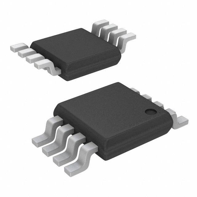
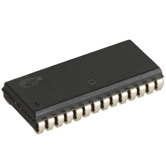
| 产品图片 |
|
| rohs | 符合RoHS无铅 / 符合限制有害物质指令(RoHS)规范要求 |
| 产品系列 | 电源管理 IC,监控电路,STMicroelectronics STM6905SYEDS6F- |
| NumberofInputsMonitored | 2 Input |
| 数据手册 | |
| 产品型号 | STM6905SYEDS6F |
| 产品培训模块 | http://www.digikey.cn/PTM/IndividualPTM.page?site=cn&lang=zhs&ptm=30015 |
| 产品目录页面 | |
| 产品种类 | 监控电路 |
| 人工复位 | Manual Reset |
| 供应商器件封装 | 8-TSSOP |
| 其它名称 | 497-8728-1 |
| 其它有关文件 | http://www.st.com/web/catalog/sense_power/FM1946/SC665/PF187297?referrer=70071840 |
| 包装 | 剪切带 (CT) |
| 受监控电压数 | 5 |
| 商标 | STMicroelectronics |
| 复位 | 低有效 |
| 复位超时 | 最小为 140 ms |
| 安装类型 | 表面贴装 |
| 安装风格 | SMD/SMT |
| 封装 | Reel |
| 封装/外壳 | 8-TSSOP,8-MSOP(0.118",3.00mm 宽) |
| 封装/箱体 | TSSOP-8 |
| 工作温度 | -40°C ~ 85°C |
| 工作电源电流 | 12 uA |
| 工厂包装数量 | 4000 |
| 最大工作温度 | + 85 C |
| 最小工作温度 | - 40 C |
| 标准包装 | 1 |
| 欠电压阈值 | 2.925 V, 2.166 V |
| 电压-阈值 | 2.188V,2.955V,可调,可调,可调 |
| 电池备用开关 | No Backup |
| 电源电压-最大 | 5.5 V |
| 电源电压-最小 | 0.8 V |
| 监视器 | No Watchdog |
| 类型 | Voltage Supervisory |
| 系列 | STM6905 |
| 被监测输入数 | 2 Input |
| 输出 | 开路漏极或开路集电极 |
| 输出类型 | Active Low, Open Drain |
| 过电压阈值 | 2.985 V, 2.21 V |
| 阈值电压 | 0.8 V to 5.5 V |


PDF Datasheet 数据手册内容提取
STM6905 Quintuple, ultralow voltage supervisor with push-button reset Datasheet - production data • 600 mV internal reference • RST output (open drain) • Output guaranteed for V ≥ 0.8 V CC • Reset delay time (T ) on power-up: 210 ms REC (typ) MSOP8 • Manual reset input (MR) (TSSOP8) (DS) • Low supply current of 12 µA (typ) • Power supply voltage 0.8 V to 5.5 V • RoHS compliant (green package) Features • 8-pin MSOP/TSSOP • Quintuple voltage monitoring • Operating temperature: –40 °C to 85 °C (industrial grade) • Accurate ±1.8 % across temperature voltage threshold (±1 % at 25 °C) Applications • Primary supply (V ) monitor. Fixed (factory - CC programmed) reset thresholds: 3.078 V to • Set-top boxes 2.866 V • Multi-voltage systems • Second fixed (V2IN) monitor. Fixed (factory- • Cable/satellite applications programmed) reset thresholds: 2.333 V to 1.050 V • Computer systems • Three additional adjustable supply monitor • Data storage equipment inputs (externally adjustable) Table 1. Device summary(1) Order code V (V) V (V) t (ms) Package RST1 RST2 REC STM6905TZEDS6F 2.333 STM6905TWEDS6F 3.078 1.683 STM6905TGEDS6F 1.110 210 MSOP8 (TSSOP8) STM6905SYEDS6F 2.188 2.955 STM6905SFEDS6F 1.050 STM6905PWEDS6F 2.866 1.683 1. Other reset threshold voltages and t time-out periods are offered. Contact local ST sales office for availability. REC October 2014 DocID14290 Rev 4 1/19 This is information on a product in full production. www.st.com
Contents STM6905 Contents 1 Description . . . . . . . . . . . . . . . . . . . . . . . . . . . . . . . . . . . . . . . . . . . . . . . . . 5 2 Pin descriptions . . . . . . . . . . . . . . . . . . . . . . . . . . . . . . . . . . . . . . . . . . . . 7 2.1 Push-button reset input (MR) . . . . . . . . . . . . . . . . . . . . . . . . . . . . . . . . . . . 7 2.2 V primary supply voltage monitoring input . . . . . . . . . . . . . . . . . . . . . . . 7 CC 2.3 V2IN second fixed voltage monitoring input . . . . . . . . . . . . . . . . . . . . . . . . 7 2.4 V SS . . . . . . . . . . . . . . . . . . . . . . . . . . . . . . . . . . . . . . . . . . . . . . . . . . . . . . . . . . . . . . . . . . . . . 7 2.5 V3IN, V4IN, and V5IN . . . . . . . . . . . . . . . . . . . . . . . . . . . . . . . . . . . . . . . . 7 2.6 RST active-low, open drain reset output . . . . . . . . . . . . . . . . . . . . . . . . . . 7 3 Operation . . . . . . . . . . . . . . . . . . . . . . . . . . . . . . . . . . . . . . . . . . . . . . . . . . 9 3.1 Setting the adjustable voltage levels for V3IN, V4IN, and V5IN inputs . . . 9 3.2 Power on reset (t ) . . . . . . . . . . . . . . . . . . . . . . . . . . . . . . . . . . . . . . . . . 9 REC 4 Voltage monitoring . . . . . . . . . . . . . . . . . . . . . . . . . . . . . . . . . . . . . . . . . 10 5 Maximum rating . . . . . . . . . . . . . . . . . . . . . . . . . . . . . . . . . . . . . . . . . . . . 11 6 DC and AC parameters . . . . . . . . . . . . . . . . . . . . . . . . . . . . . . . . . . . . . . 12 7 Package information . . . . . . . . . . . . . . . . . . . . . . . . . . . . . . . . . . . . . . . . 14 8 Part numbering . . . . . . . . . . . . . . . . . . . . . . . . . . . . . . . . . . . . . . . . . . . . 16 9 Package marking information . . . . . . . . . . . . . . . . . . . . . . . . . . . . . . . . 17 10 Revision history . . . . . . . . . . . . . . . . . . . . . . . . . . . . . . . . . . . . . . . . . . . 18 2/19 DocID14290 Rev 4
STM6905 List of tables List of tables Table 1. Device summary. . . . . . . . . . . . . . . . . . . . . . . . . . . . . . . . . . . . . . . . . . . . . . . . . . . . . . . . . . 1 Table 2. Signal names and functions . . . . . . . . . . . . . . . . . . . . . . . . . . . . . . . . . . . . . . . . . . . . . . . . . 6 Table 3. Absolute maximum ratings. . . . . . . . . . . . . . . . . . . . . . . . . . . . . . . . . . . . . . . . . . . . . . . . . 11 Table 4. DC and AC characteristics . . . . . . . . . . . . . . . . . . . . . . . . . . . . . . . . . . . . . . . . . . . . . . . . . 12 Table 5. TSSOP8 3 mm x 3 mm, package mechanical data . . . . . . . . . . . . . . . . . . . . . . . . . . . . . . 15 Table 6. Ordering information scheme. . . . . . . . . . . . . . . . . . . . . . . . . . . . . . . . . . . . . . . . . . . . . . . 16 Table 7. Marking description. . . . . . . . . . . . . . . . . . . . . . . . . . . . . . . . . . . . . . . . . . . . . . . . . . . . . . . 17 Table 8. Document revision history . . . . . . . . . . . . . . . . . . . . . . . . . . . . . . . . . . . . . . . . . . . . . . . . . 18 DocID14290 Rev 4 3/19 3
List of figures STM6905 List of figures Figure 1. Logic diagram. . . . . . . . . . . . . . . . . . . . . . . . . . . . . . . . . . . . . . . . . . . . . . . . . . . . . . . . . . . . 5 Figure 2. MSOP/TSSOP-8 connections. . . . . . . . . . . . . . . . . . . . . . . . . . . . . . . . . . . . . . . . . . . . . . . . 5 Figure 3. Functional block diagram . . . . . . . . . . . . . . . . . . . . . . . . . . . . . . . . . . . . . . . . . . . . . . . . . . . 8 Figure 4. Typical hardware hookup application diagram. . . . . . . . . . . . . . . . . . . . . . . . . . . . . . . . . . . 8 Figure 5. MR timing waveforms. . . . . . . . . . . . . . . . . . . . . . . . . . . . . . . . . . . . . . . . . . . . . . . . . . . . . 10 Figure 6. Voltage monitoring diagram . . . . . . . . . . . . . . . . . . . . . . . . . . . . . . . . . . . . . . . . . . . . . . . . 10 Figure 7. TSSOP8 3 mm x 3 mm, package mechanical outline. . . . . . . . . . . . . . . . . . . . . . . . . . . . . 15 4/19 DocID14290 Rev 4
STM6905 Description 1 Description The STM6905 supervisor is a low voltage/low supply current processor supervisor, designed to monitor up to five system power supply voltages. This device is targeted at applications such as set-top boxes (STBs), portable, battery-powered systems, networking and communication systems. The device supports a push-button type manual reset input (MR). Two of the five supply monitors (V and V2IN) have fixed (customer-selectable, factory-trimmed) thresholds CC (V and V ). The other three voltage monitor inputs (V3IN, V4IN and V5IN) are RST1 RST2 monitored using externally adjustable threshold (600 mV internal reference) to meet specific level requirements. If any of the five monitored voltages drops below its factory-trimmed or adjustable thresholds, or if the MR is asserted to logic low, the reset output RST is asserted (driven low). Once asserted, RST is maintained low for a minimum delay period (t ) after ALL REC monitored supplies rise above their respective thresholds and MR returns to high. The reset output logic state is valid for V greater than 0.8 V. CC The STM6905 is available in a standard 8-lead MSOP (TSSOP) package. Figure 1. Logic diagram V CC V2IN V3IN V4IN STM6905 RST V5IN MR V SS ai13970 Figure 2. MSOP/TSSOP-8 connections MR 1 8 RST VCC 2 7 V5IN V2IN 3 6 V4IN V 4 5 V3IN SS ai13971 DocID14290 Rev 4 5/19 18
Description STM6905 Table 2. Signal names and functions Pin Name Type Function 1 MR Input Active-low manual reset input with internal pull-up resistor Primary supply voltage input and integrated fixed threshold under- 2 V Supply CC voltage monitor 3 V2IN Input Second fixed threshold input monitor 4 V Supply Ground SS 5 V3IN Adjustable third reset comparator input 6 V4IN Input Adjustable fourth reset comparator input 7 V5IN Adjustable fifth reset comparator input 8 RST Output Active-low open-drain reset output (10 kΩ internal pull-up) 6/19 DocID14290 Rev 4
STM6905 Pin descriptions 2 Pin descriptions 2.1 Push-button reset input (MR) When MR goes low the RST output is driven low. RST remains low as long as MR is low and for the t after MR returns to high. The active-low input has an internal 10 kΩ pull-up REC resistor to V . It can be driven from a TTL or CMOS logic line, or with open drain/collector CC outputs, or connected to V through a switch. If unused, leave this pin open or connect it to SS V . CC Connect a normally open momentary switch from MR to V . An external debounce circuitry SS is not required (if MR is driven from long cables or if the device is used in noisy environments, connecting a 0.1 µF capacitor from MR to V provides additional noise SS immunity). 2.2 V primary supply voltage monitoring input CC The V pin is also the input for the primary reset threshold monitor. Fixed (customer- CC selectable, factory programmed) reset thresholds include 3.078 V to 2.866 V. 2.3 V2IN second fixed voltage monitoring input The V2IN input is the second fixed-voltage input for reset threshold monitoring. Available fixed (customer-selectable, factory programmed) reset thresholds include 2.333 V to 1.050 V. 2.4 V SS This pin is the ground pin for the power supply. 2.5 V3IN, V4IN, and V5IN The V3IN, V4IN and V5IN are high impedance inputs. RST is driven low when the voltage (VTRIP) at the pin falls below 600 mV (internal reference voltage at their respective comparators). The monitored voltage reset threshold is set with an external resistor-divider network. 2.6 RST active-low, open drain reset output The reset output (RST) pin is driven low and stays low whenever V or V2IN, or V3IN, or CC V4IN, or V5IN falls below its factory-trimmed or adjustable reset threshold or when MR goes to logic low. It remains low for t after all supply voltages being monitored rise above their REC reset thresholds and MR goes from low to high. Connect an external pull-up resistor to V . CC A 10 kΩ pull-up resistor should be sufficient for most applications. DocID14290 Rev 4 7/19 18
Pin descriptions STM6905 Figure 3. Functional block diagram VCC VRST1 COMPARE V2IN VRST2 COMPARE V3IN VREF = 0.6V COMPARE Gentreercator RST V4IN VREF = 0.6V COMPARE V5IN VREF = 0.6V COMPARE VCC (1) MR ai13970 1. Internal pull-up on MR input of 10 kΩ (typ). Figure 4. Typical hardware hookup application diagram From DC/DC Converter VCC2 VCC1 VTRIP =(600mV) (R1R +2 R2) VCC VTRIP =(600mV) (R3R +4 R4) 0.1 F STM6905 VTRIP =(600mV) (R5R +6 R6) VIN2 VCC3 0.1 F RST RST (To Processor Reset) R1 VIN3 VCC4 R2 R3 MR VIN4 Push-button R4 VCC5 Switch R5 VIN5 R6 VSS ai13973 8/19 DocID14290 Rev 4
STM6905 Operation 3 Operation The STM6905 can monitor critical voltages such as power-supply and battery voltage levels, while interfacing easily with the system controllers/microprocessors. Figure 4 shows the typical hardware hookup for monitoring five voltages: two fixed thresholds (customer-selectable, factory-programmed) and three adjustable monitor inputs. The RST output is open drain and requires a 10 kΩ pull-up resistor tied to V . CC 3.1 Setting the adjustable voltage levels for V3IN, V4IN, and V5IN inputs The user can customize the minimum voltage levels for the three adjustable voltage inputs by connecting an external resistor divider network to the V3IN, V4IN and V5IN pins in order to set the trip point at some voltage above the 600 mv (V ) according to the following REF formula. R1+R2 VTRIP = 0.6 V× ---------------------- R2 During normal operation, the STM6905 monitors the voltage levels at all five pins (Vcc, V2IN, V3IN, V4IN, and V5IN). 3.2 Power on reset (t ) REC On power up, the STM6905 activates a power-on reset circuit which asserts the reset pin (i.e. RST goes low). The RST signal remains active until V (and V2IN, V3IN, V4IN, V5IN, CC and MR) rises above the minimum voltage level for the time period t thereby ensuring REC that the supply voltage has stabilized to sufficient operating levels. DocID14290 Rev 4 9/19 18
Voltage monitoring STM6905 4 Voltage monitoring Figure 5. MR timing waveforms t MLMH MR t MLMR RST t REC ai13974 Figure 6. Voltage monitoring diagram VCC, VXIN V , RST1/2 t VRSTIN RD trec RST ai13975 10/19 DocID14290 Rev 4
STM6905 Maximum rating 5 Maximum rating Stressing the device above the ratings listed in the “Absolute maximum ratings” table may cause permanent damage to the device. These are stress ratings only and operation of the device at these or any other conditions above those indicated in the Operating sections of this specification is not implied. Exposure to absolute maximum rating conditions for extended periods may affect device reliability. Refer also to the STMicroelectronics SURE program and other relevant quality documents. Table 3. Absolute maximum ratings Symbol Parameter Value Unit T Storage temperature (V off) -55 to +150 STG CC °C T (1) Lead solder temperature for 10 seconds 260 SLD V Input or output voltage -0.3 to V +0.3 IO CC V V Supply voltage -0.3 to 7.0 CC I Output current 20 mA O θ Thermal resistance (junction to ambient) 146 °C/W JA 1. Reflow at peak temperature of 255 °C to 260 °C for < 30 seconds (total thermal budget not to exceed 180 °C for between 90 to 150 seconds). DocID14290 Rev 4 11/19 18
DC and AC parameters STM6905 6 DC and AC parameters This section summarizes the operating measurement conditions and the DC and AC characteristics of the device. Designers should check that the operating conditions in their circuit match the operating conditions when relying on the quoted parameters. Table 4. DC and AC characteristics Alter- Symbol Description Test condition(1) Min Typ Max Unit native V Operating voltage 0.8 5.5 V CC V < 5.5 V 12 16 CC I V supply current CC CC V = 3.3 V 11 15 CC I2IN V2IN supply current V2IN = 3.3 V 3 5 µA Input leakage current I V = V or V -0.5 +0.5 LI (MR)(2) IN CC SS I (3) Open drain RST output VCC > VRST, -0.5 +0.5 LO leakage current RST not asserted V ≥ 0.8 V, I = 1 µA 0.3 CC SINK V ≥ 1.0 V, I = 50 µA 0.3 CC SINK Output low voltage V V ≥ 1.2 V, I = 100 µA 0.3 OL (RST, open drain) CC SINK V ≥ 2.7 V, I = 1.2 mA 0.3 CC SINK V ≥ 4.5 V, I = 3.2 mA 0.4 CC SINK 25°C 3.047 3.078 3.109 T (falling) -40 °C to 85 °C 3.023 3.133 25 °C 2.925 2.955 2.985 V (4) V V reset threshold S (falling) RST1 TH1 CC -40 °C to 85 °C 2.902 3.008 25 °C 2.837 2.866 2.895 P (falling) -40 °C to 85 °C 2.814 2.918 V 25 °C 2.310 2.333 2.356 Z (falling) -40 °C to 85 °C 2.291 2.375 25 °C 2.166 2.188 2.210 Y (falling) -40 °C to 85 °C 2.149 2.227 25 °C 1.666 1.683 1.700 V (4) V V2IN reset threshold W (falling) RST2 TH2 -40 °C to 85 °C 1.653 1.713 25 °C 1.099 1.110 1.121 G (falling) -40 °C to 85 °C 1.090 1.130 25 °C 1.040 1.050 1.061 F (falling) -40 °C to 85 °C 1.031 1.069 12/19 DocID14290 Rev 4
STM6905 DC and AC parameters Table 4. DC and AC characteristics (continued) Alter- Symbol Description Test condition(1) Min Typ Max Unit native Reset threshold Referenced to V /V V RST1 RST2 0.5 % HYST hysteresis typical V = (V + 100 mV) to CC RST1 20 (VRST1 – 100 mV) µs t V to RST delay RD CC V2IN = (V + 75 mV) to RST2 20 (V – 75 mV) RST2 Option B(5) 20 30 40 Option C(5) 80 120 180 t t RST time-out period ms REC RP Option E 140 210 280 Option F(5) 280 420 560 Adjustable reset comparator input (V3IN, V4IN, V5IN) V3IN, V4IN, V5IN input V 589 600 611 mV RSTIN threshold V3IN, V4IN, V5IN input I V3IN, V4IN, V5IN > 0.8 V –25 +25 nA RSTIN current V3IN, V4IN, V5IN 3 mV hysteresis V3IN, V4IN, V5IN to t VRSTIN to (VRSTIN – 30 mV) 22 µs RSTIND RST output delay Manual (push-button) reset input V 0.3 x V IL CC MR input voltage V V 0.7 x V IH CC MR minimum pulse t t 1 µs MLMH MR width t t MR to RST output delay 200 MLRL MRD ns MR glitch immunity 100 MR pull-up resistance 10 kΩ 1. Valid for ambient operating temperature: T = –40 °C to +85 °C; V = 0.8 V to 5.5 V (except where noted). A CC 2. 10 kΩ (typ) internal pull-up resistor. 3. The leakage current measured on the RST pin is tested with the reset de-asserted (output high impedance). 4. Other reset threshold voltages are offered. Minimum order quantities may apply. Contact local sales office for availability. 5. Other t time-out periods are offered. Minimum order quantities may apply. Contact local sales office for availability. REC DocID14290 Rev 4 13/19 18
Package information STM6905 7 Package information In order to meet environmental requirements, ST offers these devices in different grades of ECOPACK® packages, depending on their level of environmental compliance. ECOPACK® specifications, grade definitions and product status are available at: www.st.com. ECOPACK® is an ST trademark. 14/19 DocID14290 Rev 4
STM6905 Package information Figure 7. TSSOP8 3 mm x 3 mm, package mechanical outline D 8 5 c E1 E 1 4 k A1 L L2 A A2 ccc L1 b e E3_ME Table 5. TSSOP8 3 mm x 3 mm, package mechanical data mm inches Symbol Min Typ Max Min Typ Max A 1.100 0.043 A1 0.00 0.15 0.000 0.006 A2 0.75 0.85 0.95 0.030 0.034 0.037 b 0.22 0.40 0.009 0.016 c 0.08 0.23 0.003 0.009 ccc 0.10 0.004 D 2.80 3.00 3.20 0.110 0.118 0.126 e 0.65 0.026 E 4.65 4.90 5.15 0.183 0.193 0.203 E1 2.80 3.00 3.10 0.110 0.118 0.122 L 0.40 0.60 0.80 0.016 0.024 0.032 L1 0.95 0.037 L2 0.25 0.010 k 0° 4 6° 0° 4 6° N 8 8 DocID14290 Rev 4 15/19 18
Part numbering STM6905 8 Part numbering Table 6. Ordering information scheme Example: STM6905 TZ E DS 6 F Device type STM6905 Reset threshold voltages(1) Suffix V V RST1 RST2 TZ 3.078 2.333 TW 3.078 1.683 TG 3.078 1.110 SY 2.955 2.188 SF 2.955 1.050 PW 2.866 1.683 t REC B = 30 ms(1) C = 120 ms(1) E = 210 ms F = 420 ms(1) Package DS = MSOP8 (TSSOP8) Temperature range 6: -40 °C to 85 °C Shipping method E = ECOPACK® package, tubes F = ECOPACK® package, tape and reel 1. Other reset threshold voltages and t time-out periods are offered. Minimum order quantities may REC apply. Contact local sales office for availability. 16/19 DocID14290 Rev 4
STM6905 Package marking information 9 Package marking information Table 7. Marking description Part marking V (V) V (V) Package Topside marking RST1 RST2 STM6905TZEDS6F 2.333 STZE STM6905TWEDS6F 3.078 1.683 STWE STM6905TGEDS6F 1.110 STGE MSOP (TSSOP8) STM6905SYEDS6F 2.188 SSYE 2.955 STM6905SFEDS6F 1.050 SSFE STM6905PWEDS6F 2.866 1.683 SPWE DocID14290 Rev 4 17/19 18
Revision history STM6905 10 Revision history Table 8. Document revision history Date Revision Changes 19-Dec-2007 1 Initial release. 23-Jan-2008 2 Document status upgraded to full datasheet. 28-Jan-2008 3 Updated cover page, Figure 6, and Table 4. Small text changes to English 20-Oct-2014 4 Table 1: updated footnote 1 Table 6: updated the reset threshold voltage of “SY” (V ) RST2 18/19 DocID14290 Rev 4
STM6905 IMPORTANT NOTICE – PLEASE READ CAREFULLY STMicroelectronics NV and its subsidiaries (“ST”) reserve the right to make changes, corrections, enhancements, modifications, and improvements to ST products and/or to this document at any time without notice. Purchasers should obtain the latest relevant information on ST products before placing orders. ST products are sold pursuant to ST’s terms and conditions of sale in place at the time of order acknowledgement. Purchasers are solely responsible for the choice, selection, and use of ST products and ST assumes no liability for application assistance or the design of Purchasers’ products. No license, express or implied, to any intellectual property right is granted by ST herein. Resale of ST products with provisions different from the information set forth herein shall void any warranty granted by ST for such product. ST and the ST logo are trademarks of ST. All other product or service names are the property of their respective owners. Information in this document supersedes and replaces information previously supplied in any prior versions of this document. © 2014 STMicroelectronics – All rights reserved DocID14290 Rev 4 19/19 19