ICGOO在线商城 > 集成电路(IC) > PMIC - 监控器 > STM6719TWWB6F

 Datasheet下载
- 型号: STM6719TWWB6F
- 制造商: STMicroelectronics
- 库位|库存: xxxx|xxxx
- 要求:
| 数量阶梯 | 香港交货 | 国内含税 |
| +xxxx | $xxxx | ¥xxxx |
查看当月历史价格
查看今年历史价格
STM6719TWWB6F产品简介:
ICGOO电子元器件商城为您提供STM6719TWWB6F由STMicroelectronics设计生产,在icgoo商城现货销售,并且可以通过原厂、代理商等渠道进行代购。 STM6719TWWB6F价格参考。STMicroelectronicsSTM6719TWWB6F封装/规格:PMIC - 监控器, 开路漏极或开路集电极 监控器 3 通道 SOT-23-6。您可以下载STM6719TWWB6F参考资料、Datasheet数据手册功能说明书,资料中有STM6719TWWB6F 详细功能的应用电路图电压和使用方法及教程。
STM6719TWWB6F 是意法半导体(STMicroelectronics)生产的一款电源管理IC,属于PMIC中的监控器类别。该器件主要用于监测电源电压和系统健康状况,具备复位功能,可在电压异常时确保系统稳定运行。

其主要应用场景包括:

1. 嵌入式系统与微控制器应用:用于监测微控制器或处理器的供电电压,当电压低于设定阈值时,触发复位信号,防止系统因电压不稳而出现异常运行。

2. 工业控制系统:在工业自动化设备中,STM6719TWWB6F可用于监控关键电源轨,确保控制系统的可靠性和稳定性,避免因电源问题导致设备故障。

3. 通信设备:在路由器、交换机等通信设备中,用于监控电源状态,保障设备在复杂环境中稳定运行。

4. 消费电子产品:如智能家电、智能仪表等,用于电源监控和系统复位管理,提高产品可靠性。

5. 汽车电子:适用于车载电子系统中,监控电池或电源模块的电压变化,保障车辆电子系统正常工作。

该芯片采用小型封装,功耗低,适用于对空间和能效有要求的应用场景。其电压监测阈值固定,响应时间快,适合用于对系统稳定性要求较高的场合。
| 参数 | 数值 |
| 产品目录 | 集成电路 (IC)半导体 |
| 描述 | SUPERVISOR DUAL/TRPL PP SOT23-6监控电路 Triple Ultra-Lo Volt Open Drain reset |
| 产品分类 | |
| 品牌 | STMicroelectronics |
| 产品手册 | |
| 产品图片 |
|
| rohs | 符合RoHS无铅 / 符合限制有害物质指令(RoHS)规范要求 |
| 产品系列 | 电源管理 IC,监控电路,STMicroelectronics STM6719TWWB6F- |
| NumberofInputsMonitored | 3 Input |
| 数据手册 | |
| 产品型号 | STM6719TWWB6F |
| 产品目录页面 | |
| 产品种类 | 监控电路 |
| 人工复位 | Manual Reset |
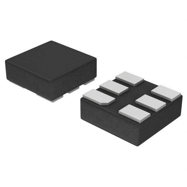
| 供应商器件封装 | SOT-23-6 |
| 其它名称 | 497-5016-1 |
| 其它有关文件 | http://www.st.com/web/catalog/sense_power/FM1946/SC665/PF99728?referrer=70071840 |
| 功率失效检测 | No |
| 包装 | 剪切带 (CT) |
| 受监控电压数 | 3 |
| 商标 | STMicroelectronics |
| 复位 | 低有效 |
| 复位超时 | 最小为 140 ms |
| 安装类型 | 表面贴装 |
| 安装风格 | SMD/SMT |
| 封装 | Reel |
| 封装/外壳 | SOT-23-6 |
| 封装/箱体 | SOT-23-6 |
| 工作温度 | -40°C ~ 85°C |
| 工作电源电流 | 35 uA |
| 工厂包装数量 | 3000 |
| 最大功率耗散 | 675 mW |
| 最大工作温度 | + 85 C |
| 最小工作温度 | - 40 C |
| 标准包装 | 1 |
| 欠电压阈值 | 3 V, 1.62 V |
| 电压-阈值 | 1.665V,3.075V,可调 |
| 电池备用开关 | No Backup |
| 电源电压-最大 | 5.5 V |
| 电源电压-最小 | 0.8 V |
| 监视器 | No Watchdog |
| 类型 | Voltage Supervisory |
| 系列 | STM6719 |
| 芯片启用信号 | No Chip Enable |
| 被监测输入数 | 3 Input |
| 输出 | 开路漏极或开路集电极 |
| 输出类型 | Active Low, Open Drain |
| 过电压阈值 | 3.15 V, 1.71 V |
| 重置延迟时间 | 280 ms |
| 阈值电压 | 0.8 V to 5.5 V |


- 商务部:美国ITC正式对集成电路等产品启动337调查
- 曝三星4nm工艺存在良率问题 高通将骁龙8 Gen1或转产台积电
- 太阳诱电将投资9.5亿元在常州建新厂生产MLCC 预计2023年完工
- 英特尔发布欧洲新工厂建设计划 深化IDM 2.0 战略
- 台积电先进制程称霸业界 有大客户加持明年业绩稳了
- 达到5530亿美元!SIA预计今年全球半导体销售额将创下新高
- 英特尔拟将自动驾驶子公司Mobileye上市 估值或超500亿美元
- 三星加码芯片和SET,合并消费电子和移动部门,撤换高东真等 CEO
- 三星电子宣布重大人事变动 还合并消费电子和移动部门
- 海关总署:前11个月进口集成电路产品价值2.52万亿元 增长14.8%


PDF Datasheet 数据手册内容提取
STM6717/6718/6719/6720 STM6777/6778/6779/6780 Dual/triple ultra-low voltage supervisors with push-button reset (with delay option) Features ■ Primary supply (V ) monitor. CC1 Fixed (factory-programmed) reset thresholds: 4.63 V to 1.58 V ■ Secondary supply (V ) monitor CC2 (STM6717/18/19/20/77/78) ■ Fixed (factory-programmed) reset thresholds: 3.08 V to 0.79 V ■ Tertiary supply monitor (using externally SOT23-5 (WY) adjustable RSTIN): 0.626 V internal reference ■ RST outputs (push-pull or open drain); state guaranteed if V or V ≥ 0.8 V CC1 CC2 ■ Reset delay time (t ) on power-up: 13.2 ms, rec 210 ms, 900 ms (typ) ■ Manual reset input (MR) ■ Optional delayed manual reset input (MRC) with external capacitor (STM6777/78/79/80) SOT23-6 (WB) ■ Low supply current - 11 µA (typ), V = V = 3.6 V CC1 CC2 ■ Operating temperature: –40 °C to 85 °C (industrial grade) Table 1. Device summary Monitored voltages Reset output (RST) Part Manual reset Delayed MR Package number input (MR) pin (MRC) Active-low Active-low V V RSTIN CC1 CC2 (push-pull) (open drain) STM6717 ✔ ✔ ✔ ✔ WY STM6718 ✔ ✔ ✔ ✔ WY STM6719 ✔ ✔ ✔ ✔ ✔ WB STM6720 ✔ ✔ ✔ ✔ ✔ WB STM6777 ✔ ✔ ✔ ✔ ✔ WB STM6778 ✔ ✔ ✔ ✔ ✔ WB STM6779 ✔ ✔ ✔ ✔ ✔ WB STM6780 ✔ ✔ ✔ ✔ ✔ WB August 2011 Doc ID 11469 Rev 8 1/30 www.st.com 1
Contents STM6717/6718/6719/6720/STM6777/6778/6779/6780 Contents 1 Description . . . . . . . . . . . . . . . . . . . . . . . . . . . . . . . . . . . . . . . . . . . . . . . . . 5 1.1 Pin descriptions . . . . . . . . . . . . . . . . . . . . . . . . . . . . . . . . . . . . . . . . . . . . . 7 1.1.1 Active-low, push-pull reset output (RST) - STM6718/20/78/80 . . . . . . . . 7 1.1.2 Active-low, open drain reset output (RST) - STM6717/19/77/79 . . . . . . . 7 1.1.3 Push-button reset input (MR) . . . . . . . . . . . . . . . . . . . . . . . . . . . . . . . . . . 7 1.1.4 Manual reset delay input (MRC) - STM6777/78/79/80) . . . . . . . . . . . . . . 8 1.1.5 Primary supply voltage monitoring input (V ) . . . . . . . . . . . . . . . . . . . 8 CC1 1.1.6 Secondary supply voltage monitoring input (V ) . . . . . . . . . . . . . . . . . 8 CC2 1.1.7 Adjustable reset comparator input (RSTIN; STM6719/20/79/80) . . . . . . 8 2 Operation . . . . . . . . . . . . . . . . . . . . . . . . . . . . . . . . . . . . . . . . . . . . . . . . . 10 2.1 Applications information . . . . . . . . . . . . . . . . . . . . . . . . . . . . . . . . . . . . . . 10 3 Typical operating characteristics . . . . . . . . . . . . . . . . . . . . . . . . . . . . . 11 4 Maximum rating . . . . . . . . . . . . . . . . . . . . . . . . . . . . . . . . . . . . . . . . . . . . 17 5 DC and AC parameters . . . . . . . . . . . . . . . . . . . . . . . . . . . . . . . . . . . . . . 18 6 Package mechanical data . . . . . . . . . . . . . . . . . . . . . . . . . . . . . . . . . . . . 22 7 Part numbering . . . . . . . . . . . . . . . . . . . . . . . . . . . . . . . . . . . . . . . . . . . . 26 8 Revision history . . . . . . . . . . . . . . . . . . . . . . . . . . . . . . . . . . . . . . . . . . . 29 2/30 Doc ID 11469 Rev 8
STM6717/6718/6719/6720/STM6777/6778/6779/6780 List of tables List of tables Table 1. Device summary. . . . . . . . . . . . . . . . . . . . . . . . . . . . . . . . . . . . . . . . . . . . . . . . . . . . . . . . . . 1 Table 2. Signal names . . . . . . . . . . . . . . . . . . . . . . . . . . . . . . . . . . . . . . . . . . . . . . . . . . . . . . . . . . . . 6 Table 3. Pin functions. . . . . . . . . . . . . . . . . . . . . . . . . . . . . . . . . . . . . . . . . . . . . . . . . . . . . . . . . . . . . 8 Table 4. Absolute maximum ratings. . . . . . . . . . . . . . . . . . . . . . . . . . . . . . . . . . . . . . . . . . . . . . . . . 17 Table 5. Operating and AC measurement conditions. . . . . . . . . . . . . . . . . . . . . . . . . . . . . . . . . . . . 18 Table 6. DC and AC characteristics . . . . . . . . . . . . . . . . . . . . . . . . . . . . . . . . . . . . . . . . . . . . . . . . . 19 Table 7. t minimum pulse width . . . . . . . . . . . . . . . . . . . . . . . . . . . . . . . . . . . . . . . . . . . . . . . . 21 MLMH Table 8. SOT23-5 – 5-lead small outline transistor package mechanical data. . . . . . . . . . . . . . . . . 23 Table 9. SOT23-6 – 6-lead small outline transistor package mechanical data. . . . . . . . . . . . . . . . . 24 Table 10. Carrier tape dimensions for SOT23-5L and SOT23-6L . . . . . . . . . . . . . . . . . . . . . . . . . . . 25 Table 11. Ordering information scheme. . . . . . . . . . . . . . . . . . . . . . . . . . . . . . . . . . . . . . . . . . . . . . . 26 Table 12. Marking description. . . . . . . . . . . . . . . . . . . . . . . . . . . . . . . . . . . . . . . . . . . . . . . . . . . . . . . 27 Table 13. Document revision history . . . . . . . . . . . . . . . . . . . . . . . . . . . . . . . . . . . . . . . . . . . . . . . . . 29 Doc ID 11469 Rev 8 3/30
List of figures STM6717/6718/6719/6720/STM6777/6778/6779/6780 List of figures Figure 1. Logic diagram (STM6717/18). . . . . . . . . . . . . . . . . . . . . . . . . . . . . . . . . . . . . . . . . . . . . . . . 6 Figure 2. Logic diagram (STM6777/78). . . . . . . . . . . . . . . . . . . . . . . . . . . . . . . . . . . . . . . . . . . . . . . . 6 Figure 3. Logic diagram (STM6719/20). . . . . . . . . . . . . . . . . . . . . . . . . . . . . . . . . . . . . . . . . . . . . . . . 6 Figure 4. Logic diagram (STM6779/80). . . . . . . . . . . . . . . . . . . . . . . . . . . . . . . . . . . . . . . . . . . . . . . . 6 Figure 5. STM6717/18 SOT23-5 connections. . . . . . . . . . . . . . . . . . . . . . . . . . . . . . . . . . . . . . . . . . . 7 Figure 6. STM6777/78 SOT23-6 connections. . . . . . . . . . . . . . . . . . . . . . . . . . . . . . . . . . . . . . . . . . . 7 Figure 7. STM6719/20 SOT23-6 connections. . . . . . . . . . . . . . . . . . . . . . . . . . . . . . . . . . . . . . . . . . . 7 Figure 8. STM6779/80 SOT23-6 connections. . . . . . . . . . . . . . . . . . . . . . . . . . . . . . . . . . . . . . . . . . . 7 Figure 9. Block diagram. . . . . . . . . . . . . . . . . . . . . . . . . . . . . . . . . . . . . . . . . . . . . . . . . . . . . . . . . . . . 9 Figure 10. Hardware hookup. . . . . . . . . . . . . . . . . . . . . . . . . . . . . . . . . . . . . . . . . . . . . . . . . . . . . . . . . 9 Figure 11. STM67xx interface to processor with bi-directional reset pins . . . . . . . . . . . . . . . . . . . . . . 10 Figure 12. Ensuring RST valid to V = 0 (active-low, push-pull outputs). . . . . . . . . . . . . . . . . . . . . . 10 CC Figure 13. Supply current vs. temperature (V = 5.5 V; V = 3.6 V) . . . . . . . . . . . . . . . . . . . . . . 11 CC1 CC2 Figure 14. Supply current vs. temperature (V = 3.6 V; V = 2.75 V) . . . . . . . . . . . . . . . . . . . . . 11 CC1 CC2 Figure 15. Supply current vs. temperature (V = 3.0 V; V = 2.0 V) . . . . . . . . . . . . . . . . . . . . . . 12 CC1 CC2 Figure 16. Supply current vs. temperature (V = 2.0 V; V = 1.0 V) . . . . . . . . . . . . . . . . . . . . . . 12 CC1 CC2 Figure 17. Normalized V reset time-out period vs. temperature . . . . . . . . . . . . . . . . . . . . . . . . . . . 13 CC Figure 18. Maximum V transient duration vs. reset threshold overdrive . . . . . . . . . . . . . . . . . . . . . 13 CC Figure 19. Normalized V threshold vs. temperature. . . . . . . . . . . . . . . . . . . . . . . . . . . . . . . . . . . 14 RST1 Figure 20. Normalized V threshold vs. temperature. . . . . . . . . . . . . . . . . . . . . . . . . . . . . . . . . . . 14 RST2 Figure 21. Reset input threshold vs. temperature . . . . . . . . . . . . . . . . . . . . . . . . . . . . . . . . . . . . . . . . 15 Figure 22. V -to-reset delay vs. temperature. . . . . . . . . . . . . . . . . . . . . . . . . . . . . . . . . . . . . . . . . . 15 CC1 Figure 23. Reset input-to-reset output delay vs. temperature . . . . . . . . . . . . . . . . . . . . . . . . . . . . . . . 16 Figure 24. MR-to-reset output delay vs. temperature (V = 3.6V). . . . . . . . . . . . . . . . . . . . . . . . . . 16 CC1 Figure 25. AC testing input/output waveforms. . . . . . . . . . . . . . . . . . . . . . . . . . . . . . . . . . . . . . . . . . . 18 Figure 26. MR timing waveform (STM6717/18/19/20). . . . . . . . . . . . . . . . . . . . . . . . . . . . . . . . . . . . . 18 Figure 27. MR timing waveform (STM6777/78/79/80). . . . . . . . . . . . . . . . . . . . . . . . . . . . . . . . . . . . . 18 Figure 28. SOT23-5 – 5-lead small outline transistor package mechanical drawing. . . . . . . . . . . . . . 23 Figure 29. SOT23-6 – 6-lead small outline transistor package mechanical drawing. . . . . . . . . . . . . . 24 Figure 30. Carrier tape for SOT23-5L and SOT23-6L. . . . . . . . . . . . . . . . . . . . . . . . . . . . . . . . . . . . . 25 4/30 Doc ID 11469 Rev 8
STM6717/6718/6719/6720/STM6777/6778/6779/6780 Description 1 Description The STM6717/18/19/20 and STM6777/78/79/80 supervisors are a family of low-voltage/low- supply current processor (micro or DSP) supervisors, designed to monitor two (or three) system power supply voltages. They are targeted at applications such as set-top boxes (STBs), portable, battery-powered systems, networking, and communication systems. All device options have a push-button-type manual reset input (MR). The STM6777/78/79/80 also includes an option which enables the user to delay the start of the manual reset process from 6 µs (MRC pin left open) or more with external capacitor. The delay is implemented by connecting the appropriately sized capacitor between the MRC pin and V (typical 4 s delay with a 3.3 µF capacitor, see Table7 on page21). SS Two of the three supplies monitored (V and V ) have fixed (customer-selectable, CC1 CC2 factory-trimmed) thresholds (V and V ). The third voltage is monitored using an RST1 RST2 externally adjustable RSTIN threshold (0.626 V internal reference). If any of the three monitored voltages drop below its factory-trimmed or adjustable thresholds, or if MR is asserted to logic low, a RST is asserted (driven low). Once asserted, RST is maintained at low for a minimum delay period (t ) after ALL supplies rise above rec their respective thresholds and MR returns to high. These devices are guaranteed to be in the correct reset output logic state when V and/or V is greater than 0.8 V. CC1 CC2 These devices are available in standard 5-pin or 6-pin SOT23 packages (see Table1 on page1). Doc ID 11469 Rev 8 5/30
Description STM6717/6718/6719/6720/STM6777/6778/6779/6780 Figure 1. Logic diagram (STM6717/18) Figure 2. Logic diagram (STM6777/78) VCC2 VCC1 VCC2 VCC1 MRC STM6717 STM6777 MR STM6718 RST STM6778 RST MR VSS VSS AI10413 AI10415 Figure 3. Logic diagram (STM6719/20) Figure 4. Logic diagram (STM6779/80) VCC2 VCC1 VCC RSTIN RSTIN STM6719 STM6779 STM6720 RST MRC STM6780 RST MR MR VSS VSS AI10414 AI10416 Table 2. Signal names MR Push-button reset input MRC Manual reset delay input RST Active-low reset output V Primary supply voltage input CC1 V Secondary supply voltage input CC2 RSTIN Adjustable reset comparator input V Ground SS 6/30 Doc ID 11469 Rev 8
STM6717/6718/6719/6720/STM6777/6778/6779/6780 Description Figure 5. STM6717/18 SOT23-5 connections Figure 6. STM6777/78 SOT23-6 connections RST 1 5 VCC1 RST 1 6 VCC1 VSS 2 VSS 2 5 MRC MR 3 4 VCC2 MR 3 4 VCC2 AI10417 AI10418 Figure 7. STM6719/20 SOT23-6 connections Figure 8. STM6779/80 SOT23-6 connections RST 1 6 VCC1 RST 1 6 VCC1 VSS 2 5 RSTIN VSS 2 5 RSTIN MR 3 4 VCC2 MR 3 4 MRC AI10419 AI10420 1.1 Pin descriptions 1.1.1 Active-low, push-pull reset output (RST) - STM6718/20/78/80 The RST pin is driven low and stays low whenever V or V or RSTIN falls below its CC1 CC2 factory-trimmed or adjustable reset threshold or when MR goes to logic low. It remains low for t after ALL supply voltages being monitored rise above their reset thresholds and MR rec goes from low to high. (Push-pull outputs are referenced to V .) CC1 1.1.2 Active-low, open drain reset output (RST) - STM6717/19/77/79 The RST pin is driven low and stays low whenever V or V or RSTIN falls below its CC1 CC2 factory-trimmed or adjustable reset threshold or when MR goes to logic low. It remains low for t after ALL supply voltages being monitored rise above their reset thresholds and MR rec goes from low to high. Connect an external pull-up resistor to V . A 10 kΩ pull-up resistor CC1 should be sufficient for most applications. 1.1.3 Push-button reset input (MR) When MR goes low the RST output is driven low. RST remains low as long as MR is low and for t after MR returns to high. This active-low input has an internal 50 kΩ pull-up resistor to rec Doc ID 11469 Rev 8 7/30
Description STM6717/6718/6719/6720/STM6777/6778/6779/6780 V . It can be driven from a TTL or CMOS logic line, or with open drain/collector outputs, CC1 or connected to V through a switch. If unused, leave this pin open or connect it to V . SS CC1 Connect a normally open momentary switch from MR to V ; external debounce circuitry is SS not required. (If MR is driven from long cables or if the device is used in noisy environments, connecting a 0.1µF capacitor from MR to V provides additional noise immunity. SS 1.1.4 Manual reset delay input (MRC) - STM6777/78/79/80) This pin is either left open or connected to V via a capacitor. By selecting the appropriate SS capacitor, the manual reset process, initiated by pressing the push-button manual reset input, can be delayed by any value from 6 µs or more (see Table7 on page21). 1.1.5 Primary supply voltage monitoring input (V ) CC1 It also is the input for the primary reset threshold monitor. Available fixed (customer- selectable, factory-programmed) reset thresholds include 4.63 V to 1.58 V. 1.1.6 Secondary supply voltage monitoring input (V ) CC2 This function is available on the STM6717/18/19/20/77/78. Fixed (customer-selectable, factory-programmed) reset thresholds include 3.08 V to 0.79 V. 1.1.7 Adjustable reset comparator input (RSTIN; STM6719/20/79/80) This is a high impedance input. RST is driven low when the voltage at the RSTIN pin falls below 0.626 V (internal reference voltage at this comparator). The monitored voltage reset threshold is set with an external resistor-divider network. T able 3. Pin functions Pin Name Function STM6717 STM6719 STM6777 STM6779 STM6718 STM6720 STM6778 STM6780 1 1 1 1 RST Active-low reset output 3 3 3 3 MR Push-button reset input — — 5 4 MRC Manual reset delay input 5 6 6 6 V Primary supply voltage input CC1 4 4 4 — V Secondary supply voltage input CC2 — 5 — 5 RSTIN Adjustable reset comparator input 2 2 2 2 V Ground SS 8/30 Doc ID 11469 Rev 8
STM6717/6718/6719/6720/STM6777/6778/6779/6780 Description Figure 9. Block diagram VCC1 VRST1 COMPARE VCC2(1) VRST2 COMPARE RSTIN(2) VCC1 VREF/2 = 0.626 COMPARE Gentreercator RST MR Logic MRC(3) AI10421 1. V input is available on STM6717/18/19/20/77/78. CC2 2. RSTIN available only on STM6719/20/79/80. 3. MRC available only on STM6777/78/79/80. Figure 10. Hardware hookup From DC/DC Converter VCC2(1) VCC1 VCC1 VCC3 =(626.5mV)(R1R +2 R2) 0.1µF STM67xx VCC2 VCC3 0.1µF R1 RSTIN(2) RST RST (To Processor Reset) R2 MR Push-button MRC(3) Switch VSS C AI10422 1. V is available only on STM6717/18/19/20/77/78. CC2 2. RSTIN available only on STM6719/20/79/80. 3. MRC available only on STM6777/78/79/80. Doc ID 11469 Rev 8 9/30
Operation STM6717/6718/6719/6720/STM6777/6778/6779/6780 2 Operation 2.1 Applications information 1. Interfacing to processors with bi-directional reset pins Most processors with bi-directional reset pins can interface directly to the open drain RST outputs (STM6717/19/77/79). Systems simultaneously requiring a push-pull RST output and a bi-directional reset interface can be in logic contention. To prevent this contention, connect a 4.7 kΩ resistor between RST and the processor’s reset I/O as shown in Figure11. 2. Ensuring a valid RST output down to V =0 V CC The STM67xx supervisors are guaranteed to be in the correct RST output logic state when V and/or V is greater than 0.8 V. In applications which require valid reset CC1 CC2 levels down to V = 0, a pull-down resistor to active-low outputs (push-pull only, see CC Figure12) will ensure that the reset line is valid while the reset output can no longer sink or source current. This scheme does NOT work with the open drain outputs of the STM6717/19/77/79. The resistor value used is not critical, but it must be large enough not to load the reset output when V is above the reset threshold. For most applications, 100 kΩ is CC adequate. Figure 11. STM67xx interface to processor with bi-directional reset pins VCC2 VCC1 STM67xx Processor To other VCC1 system components VCC2 RST RESET 4.7kΩ VSS VSS AI10425 Figure 12. Ensuring RST valid to V = 0 (active-low, push-pull outputs) CC STM67xx VCC1 VCC1 RST VSS R1 AI10426 10/30 Doc ID 11469 Rev 8
STM6717/6718/6719/6720/STM6777/6778/6779/6780 Typical operating characteristics 3 Typical operating characteristics Note: Typical values are at T = 25 °C unless otherwise noted. A Figure 13. Supply current vs. temperature (V = 5.5 V; V = 3.6 V) CC1 CC2 18 16 14 A) nt (µ 12 ITOTAL e 10 r r u y c 8 ICC1 pl p 6 u S 4 2 I CC2 0 –40 –20 0 20 40 60 80 Temperature (°C) AI11843 Figure 14. Supply current vs. temperature (V = 3.6 V; V = 2.75 V) CC1 CC2 18 16 14 A)12 µ nt ( urre10 ITOTAL ply c 8 ICC1 p u 6 S 4 ICC2 2 0 –40 –20 0 20 40 60 80 Temperature (°C) AI11844 Doc ID 11469 Rev 8 11/30
Typical operating characteristics STM6717/6718/6719/6720/STM6777/6778/6779/6780 Figure 15. Supply current vs. temperature (V = 3.0 V; V = 2.0 V) CC1 CC2 18 16 14 A) µ 12 nt ( e 10 r ur ITOTAL c 8 y pl p 6 u ICC1 S 4 2 ICC2 0 –40 –20 0 20 40 60 80 Temperature (°C) AI11845 Figure 16. Supply current vs. temperature (V = 2.0 V; V = 1.0 V) CC1 CC2 18 16 14 A) µ 12 nt ( e 10 r r u c 8 y ITOTAL pl p 6 Su ICC1 4 2 ICC2 0 –40 –20 0 20 40 60 80 Temperature (°C) AI11846 12/30 Doc ID 11469 Rev 8
STM6717/6718/6719/6720/STM6777/6778/6779/6780 Typical operating characteristics Figure 17. Normalized V reset time-out period vs. temperature CC 1.07 1.05 d o ri 1.03 e p et s e 1.01 R 0.99 0.97 –40 –20 0 20 40 60 80 Temperature (°C) AI11847 Figure 18. Maximum V transient duration vs. reset threshold overdrive CC 1000 ) s µ ( n o ti a r u d 100 t n e si n a r t C C 10 V m u m xi a M 1 1 10 100 1000 Reset threshold overdrive (mV) AI11848 Doc ID 11469 Rev 8 13/30
Typical operating characteristics STM6717/6718/6719/6720/STM6777/6778/6779/6780 Figure 19. Normalized V threshold vs. temperature RST1 1.004 d ol 1.002 h s e r h et t 1.000 s e r 1 T S R 0.998 V 0.996 –40 –20 0 20 40 60 80 Temperature (°C) AI11849 Figure 20. Normalized V threshold vs. temperature RST2 1.004 d ol 1.002 h s e r h et t 1.000 s e r 2 T S R 0.998 V 0.996 –40 –20 0 20 40 60 80 Temperature (°C) AI11850 14/30 Doc ID 11469 Rev 8
STM6717/6718/6719/6720/STM6777/6778/6779/6780 Typical operating characteristics Figure 21. Reset input threshold vs. temperature 630 V) 629 m d ( ol 628 h s e r h 627 ut t p n 626 et i s e R 625 624 –40 –20 0 20 40 60 80 Temperature (°C) AI11851 Figure 22. V -to-reset delay vs. temperature CC1 48 s) 44 µ y ( a el 40 d et s e o-r 36 -t1 C C V 32 28 –40 –20 0 20 40 60 80 Temperature (°C) AI11852 Doc ID 11469 Rev 8 15/30
Typical operating characteristics STM6717/6718/6719/6720/STM6777/6778/6779/6780 Figure 23. Reset input-to-reset output delay vs. temperature 29.0 s) 28.5 µ y ( a 28.0 el d ut 27.5 p ut o 27.0 et es 26.5 r o- N-t 26.0 TI S 25.5 R 25.0 –40 –20 0 20 40 60 80 Temperature (°C) AI11853 Figure 24. MR-to-reset output delay vs. temperature (V = 3.6V) CC1 500 s) n 480 y ( a el d ut 460 p ut o et 440 s e r o- R-t 420 M 400 –40 –20 0 20 40 60 80 Temperature (°C) AI11854 16/30 Doc ID 11469 Rev 8
STM6717/6718/6719/6720/STM6777/6778/6779/6780 Maximum rating 4 Maximum rating Stressing the device above the rating listed in the Absolute Maximum Ratings” table may cause permanent damage to the device. These are stress ratings only and operation of the device at these or any other conditions above those indicated in the Operating sections of this specification is not implied. Exposure to Absolute Maximum Rating conditions for extended periods may affect device reliability. Refer also to the STMicroelectronics SURE Program and other relevant quality documents. T able 4. Absolute maximum ratings Symbol Parameter Value Unit T Storage temperature (V off) –55 to 150 °C STG CC T (1) Lead solder temperature for 10 seconds 260 °C SLD –0.3 to V + 0.3 V CC1 V Input or output voltage IO –0.3 to V + 0.3 V CC2 V V Supply voltage –0.3 to 7.0 V CC1, CC2 I Input or output current (all pins) 20 mA IO SOT23-5 654 mW P Power dissipation D SOT23-6 675 mW 1. Reflow at peak temperature of 260 °C. The time above 255 °C must not exceed 30 seconds. Doc ID 11469 Rev 8 17/30
DC and AC parameters STM6717/6718/6719/6720/STM6777/6778/6779/6780 5 DC and AC parameters This section summarizes the operating measurement conditions, and the DC and AC characteristics of the device. The parameters in the DC and AC characteristics tables that follow, are derived from tests performed under the measurement conditions summarized in Table5: Operating and AC measurement conditions. Designers should check that the operating conditions in their circuit match the operating conditions when relying on the quoted parameters. T able 5. Operating and AC measurement conditions Parameter STM67xx Unit V supply voltage 0.8 to 5.5 V CC Ambient operating temperature (T ) –40 to 85 °C A Input rise and fall times ≤ 5 ns Input pulse voltages 0.2 to 0.8V V CC Input and output timing ref. voltages 0.3 to 0.7V V CC Figure 25. AC testing input/output waveforms 0.8VCC 0.7VCC 0.3VCC 0.2VCC AI02568 Figure 26. MR timing waveform (STM6717/18/19/20) t MLMH MR t MLRL RST t rec AI10423a Figure 27. MR timing waveform (STM6777/78/79/80) t (1) MLMH MR t MLRL RST trec AI10424c 1. By connecting a certain capacitor between the MRC pin and V , the RST can be delayed from 6 µs or SS more (t , see Table7 on page21). MLMH 18/30 Doc ID 11469 Rev 8
STM6717/6718/6719/6720/STM6777/6778/6779/6780 DC and AC parameters Table 6. D C and AC characteristics Alter- Sym Description Test condition(1) Min Typ Max Unit native V Operating voltage 0.8 5.5 V CC V < 5.5 V, all I/O pins open 12 35 µA CC1 I V supply current CC1 CC1 V < 3.6 V, all I/O pins open 8 23 µA CC1 V < 3.6 V, all I/O pins open 3 9 µA CC2 I V supply current CC2 CC2 V < 2.75 V, all I/O pins open 2.5 7 µA CC2 I (2) Input leakage current 0 V = V = V –1 +1 µA LI IN CC I Open drain RST output VCC1 > VRST1, VCC2 > VRST2; 0.5 µA LO leakage current RST not asserted V or V ≥ 0.8 V, CC1 CC2 0.3 V I = 1 µA, RST asserted SINK V or V ≥ 1.0 V, CC1 CC2 0.3 V I = 50 µA, RST asserted SINK V Output low voltage (RST; VCC1 or VCC2 ≥ 1.2 V, 0.3 V OL push-pull or open drain) I = 100 µA, RST asserted SINK V or V ≥ 2.7 V, CC1 CC2 0.3 V I = 1.2 mA, RST asserted SINK V or V ≥ 4.5 V, CC1 CC2 0.4 V I = 3.2 mA, RST asserted SINK V ≥ 1.8 V, I = 200 µA, CC1 SOURCE 0.8V V RST not asserted CC1 Output high voltage (RST; V ≥ 2.7 V, I = 500 µA, V CC1 SOURCE 0.8V V OH push-pull only) RST not asserted CC1 V ≥ 4.5 V, I = 800 µA, CC1 SOURCE 0.8V V RST not asserted CC1 Rise time measured from 10% to Push-pull RST rise time tR(3) (STM6718/20/78/80) 90% of VCC; 5 25 ns C = 5 pF, V = 3.3 V L CC Reset thresholds L (falling) 4.500 4.625 4.750 V M (falling) 4.250 4.375 4.500 V T (falling) 3.000 3.075 3.150 V S (falling) 2.850 2.925 3.000 V V (4) V V reset threshold R (falling) 2.550 2.625 2.700 V RST TH1 CC1 Z (falling) 2.250 2.313 2.375 V Y (falling) 2.125 2.188 2.250 V W (falling) 1.620 1.665 1.710 V V (falling) 1.530 1.575 1.620 V Doc ID 11469 Rev 8 19/30
DC and AC parameters STM6717/6718/6719/6720/STM6777/6778/6779/6780 Table 6. DC and AC characteristics (continued) Alter- Sym Description Test condition(1) Min Typ Max Unit native T (falling) 3.000 3.075 3.150 V S (falling) 2.850 2.925 3.000 V R (falling) 2.550 2.625 2.700 V Z (falling) 2.250 2.313 2.375 V Y (falling) 2.125 2.188 2.250 V W (falling) 1.620 1.665 1.710 V V (falling) 1.530 1.575 1.620 V V (4) V V reset threshold I (falling) 1.350 1.388 1.425 V RST2 TH2 CC2 H (falling) 1.275 1.313 1.350 V G (falling) 1.080 1.110 1.140 V F (falling) 1.020 1.050 1.080 V K (falling) 0.895 0.925 0.955 V J (falling) 0.845 0.875 0.905 V E (falling) 0.810 0.833 0.855 V D (falling) 0.765 0.788 0.810 V V Reset threshold hysteresis Referenced to V typical 0.5 % HYST RST V = (V + 100 mV) to CC1 RST1 20 µs (V – 100 mV) RST t V to RST delay RD CC V = (V + 75 mV) to CC2 RST2 20 µs (V – 75 mV) RST2 blank 140 210 280 t t RST pulse width B 8.8 13.2 17.6 ms rec RP G 600 900 1200 Adjustable reset comparator input (STM6719/20/79/80) V RSTIN input threshold 611 626.5 642 mV RSTIN I RSTIN input current –25 +25 nA RSTIN RSTIN hysteresis 3 mV RSTIN to RST t V to (V – 30 mV) 22 µs RSTIND output delay RSTIN RSTIN 20/30 Doc ID 11469 Rev 8
STM6717/6718/6719/6720/STM6777/6778/6779/6780 DC and AC parameters Table 6. DC and AC characteristics (continued) Alter- Sym Description Test condition(1) Min Typ Max Unit native Manual (push-button) reset input 0.3V V C V IL MR input voltage C1 V 0.7V V IH CC1 MR minimum pulse width 1 µs (STM6717/18/19/20) t t MLMH MR MR minimum pulse width MRC connected via 6 µs (STM6777/78/79/80) capacitor to V SS t t MR to RST output delay 200 ns MLRL MRD MR glitch immunity 100 ns (STM6717/18/19/20) MR pull-up resistance 25 50 80 kΩ 1. Valid for ambient operating temperature: T = –40 to 85 °C; V = 0.8 to 5.5 V and V = 0.8 to 3.6 V (except where A CC1 CC2 noted). 2. Input leakage for the MRC pin is not tested. 3. Guaranteed by design. 4. The leakage current measured on the RST pin is tested with the reset de-asserted (output high impedance). Table 7. t minimum pulse width MLMH Capacitor value(1) V CC1 100 pF 0.1 µF 2.2 µF 3.3 µF 4.7 µF 6.8 µF 1.6 V 120 µs 120 ms 2.6 s 4.0 s 5.6 s 8.2 s 2.0 V 122 µs 122 ms 2.7 s 4.0 s 5.8 s 8.3 s 3.0 V 125 µs 125 ms 2.7 s 4.1 s 5.9 s 8.5 s 4.0 V 128 µs 129 ms 2.8 s 4.2 s 6.0 s 8.7 s 5.0 V 130 µs 130 ms 2.8 s 4.3 s 6.1 s 8.8 s 1. At 25 °C (typical) Doc ID 11469 Rev 8 21/30
Package mechanical data STM6717/6718/6719/6720/STM6777/6778/6779/6780 6 Package mechanical data In order to meet environmental requirements, ST offers these devices in different grades of ECOPACK® packages, depending on their level of environmental compliance. ECOPACK® specifications, grade definitions and product status are available at: www.st.com. ECOPACK® is an ST trademark. 22/30 Doc ID 11469 Rev 8
STM6717/6718/6719/6720/STM6777/6778/6779/6780 Package mechanical data Figure 28. SOT23-5 – 5-lead small outline transistor package mechanical drawing E A1 1 e e1 D 5x b 5x 0.20MCAB A C0.10 A2 C Datum A A 0.20 θ C B L E1 0133778 Note: Drawing is not to scale. T able 8. SOT23-5 – 5-lead small outline transistor package mechanical data mm inches Symb Min Typ Max Min Typ Max A — — 1.45 — — 0.057 A1 — — 0.15 — — 0.006 A2 0.90 1.15 1.30 0.035 0.045 0.051 b 0.30 — 0.50 0.012 — 0.020 C 0.08 — 0.22 0.003 — 0.009 D — 2.90 — — 0.114 — E — 2.80 — — 0.110 — E1 — 1.60 — — 0.063 — e — 0.95 — — 0.037 — e1 — 1.90 — — 0.075 — L 0.30 0.45 0.60 0.012 0.018 0.024 Q 0° 4° 8° 0° 4° 8° N 5 5 Note: Dimensions per JEDEC SOT/SOP product outline MO-178C, variation AA Doc ID 11469 Rev 8 23/30
Package mechanical data STM6717/6718/6719/6720/STM6777/6778/6779/6780 Figure 29. SOT23-6 – 6-lead small outline transistor package mechanical drawing E A1 1 e e1 D 6x b 6x 0.10MCAB A C0.10 A2 C Datum A A 0.20 θ C B L E1 7049714 Note: Drawing is not to scale. T able 9. SOT23-6 – 6-lead small outline transistor package mechanical data mm inches Symb Min Typ Max Min Typ Max A — — 1.45 — — 0.057 A1 — — 0.15 — — 0.006 A2 0.90 1.15 1.30 0.035 0.045 0.051 b 0.30 — 0.50 0.012 — 0.020 C 0.08 — 0.22 0.003 — 0.009 D — 2.90 — — 0.114 — E — 2.80 — — 0.110 — E1 — 1.60 — — 0.063 — e — 0.95 — — 0.037 — e1 — 1.90 — — 0.075 — L 0.30 0.45 0.60 0.012 0.018 0.024 Q 0° 4° 8° 0° 4° 8° N 6 6 Note: Dimensions per JEDEC SOT/SOP product outline MO-178C variation AB 24/30 Doc ID 11469 Rev 8
STM6717/6718/6719/6720/STM6777/6778/6779/6780 Package mechanical data Figure 30. Carrier tape for SOT23-5L and SOT23-6L P0 E D P2 T A0 F TOP COVER TAPE W B0 CENTER LINES P1 OF CAVITY K0 USER DIRECTION OF FEED AM03073v1 Note: Part pin 1 indicator is on bottom left for shipping method “F” and is on top right for shipping method “R” see Section7. Table 10. Carrier tape dimensions for SOT23-5L and SOT23-6L Bulk Package W D E P P F A B K P T Unit 0 2 0 0 0 1 Qty 8.00 1.50 SOT23-5 1.75 4.00 2.00 3.50 3.23 3.17 1.37 4.00 0.254 +0.30/ +0.10/ mm 3000 SOT23-6 ±0.10 ±0.10 ±0.10 ±0.05 ±0.10 ±0.10 ±0.10 ±0.10 ±0.013 –0.10 –0.00 Doc ID 11469 Rev 8 25/30
Part numbering STM6717/6718/6719/6720/STM6777/6778/6779/6780 7 Part numbering Table 11. O rdering information scheme Example: STM67xx LT WY 6 F Device type STM67xx Reset thresholds (V and V ) for V and V RST1 RST2 CC1 CC2 STM6717/18/19/20/77/78 (V and V ) STM6779/80 (V only) RST1 RST2 RST1 Suffix V V Suffix V RST1 RST2 RST1 LT 4.625 3.075 L–(1) 4.625 MS 4.375 2.925 T–(1) 3.075 MR 4.375 2.625 S–(1) 2.925 TZ(1) 3.075 2.313 Y–(1) 2.188 TW(1) 3.075 1.665 V–(1) 1.575 TI 3.075 1.388 R– 2.625 TG(1) 3.075 1.110 Z– 2.313 TK 3.075 0.925 TE 3.075 0.833 SY(1) 2.925 2.188 SV(1) 2.925 1.575 SH(2) 2.925 1.313 SF(1) 2.925 1.050 SJ(3) 2.925 0.875 SD(3) 2.925 0.788 YV 2.188 1.575 YH 2.188 1.313 YF 2.188 1.050 YJ 2.188 0.875 YD 2.188 0.788 VH 1.575 1.313 VF 1.575 1.050 VJ 1.575 0.875 VD 1.575 0.788 Reset pulse width blank: t = 140 ms to 280 ms rec B: t = 8.8 ms to 17.6 ms rec G: t = 600 ms to 1200 ms rec Package WY = SOT23-5 WB = SOT23-6 Temperature range 6 = –40 to 85°C Shipping method E = ECOPACK® package, tubes F = ECOPACK® package, tape and reel R(4) = ECOPACK® package, tape and reel (pin 1 at top right). 1. These are standard versions and are typically held in stock. A non-standard version may require a higher minimum volumes, and/or longer delivery times. For other options, or for more information on any aspect of this device, please contact the ST sales office nearest you. 2. Available in STM6719 version only. 3. Available in STM6717 version only. 4. Available for STM6720SY, STM6719SF and STM6719SFB versions only. 26/30 Doc ID 11469 Rev 8
STM6717/6718/6719/6720/STM6777/6778/6779/6780 Part numbering Table 12. M arking description Part number V threshold (V) V threshold (V) Topside marking Bottomside marking RST1 RST2 STM6717SD 2.925 0.788 7SD1 PYWW STM6717SJ 2.925 0.875 7SJ1 PYWW STM6717SF 2.925 1.050 7SF1 PYWW STM6717TG 3.075 1.110 7TG1 PYWW STM6717TGG 3.075 1.110 7TG9 PYWW STM6717TW 3.075 1.665 7TW1 PYWW STM6717SV 2.925 1.575 7SV1 PYWW STM6717SY 2.925 2.188 7SY1 PYWW STM6717TZ 3.075 2.313 7TZ1 PYWW STM6718SF 2.925 1.050 7SF2 PYWW STM6718TG 3.075 1.110 7TG2 PYWW STM6718TW 3.075 1.665 7TW2 PYWW STM6718SV 2.925 1.575 7SV2 PYWW STM6718SY 2.925 2.188 7SY2 PYWW STM6718TZ 3.075 2.313 7TZ2 PYWW STM6719SF 2.925 1.050 7SF3 PYWW STM6719SFB 2.925 1.050 7SFB PYWW STM6719TG 3.075 1.110 7TG3 PYWW STM6719SH 2.925 1.313 7SH3 PYWW STM6719TW 3.075 1.665 7TW3 PYWW STM6719SV 2.925 1.575 7SV3 PYWW STM6719SY 2.925 2.188 7SY3 PYWW STM6719TZ 3.075 2.313 7TZ3 PYWW STM6720SF 2.925 1.050 7SF4 PYWW STM6720TG 3.075 1.110 7TG4 PYWW STM6720TW 3.075 1.665 7TW4 PYWW STM6720SV 2.925 1.575 7SV4 PYWW STM6720SY 2.925 2.188 7SY4 PYWW STM6720TZ 3.075 2.313 7TZ4 PYWW STM6777SF 2.925 1.050 7SF5 PYWW STM6777TG 3.075 1.110 7TG5 PYWW STM6777TW 3.075 1.665 7TW5 PYWW STM6777SV 2.925 1.575 7SV5 PYWW STM6777SY 2.925 2.188 7SY5 PYWW STM6777TZ 3.075 2.313 7TZ5 PYWW Doc ID 11469 Rev 8 27/30
Part numbering STM6717/6718/6719/6720/STM6777/6778/6779/6780 Table 12. Marking description (continued) Part number V threshold (V) V threshold (V) Topside marking Bottomside marking RST1 RST2 STM6778SF 2.925 1.050 7SF6 PYWW STM6778TG 3.075 1.110 7TG6 PYWW STM6778TW 3.075 1.665 7TW6 PYWW STM6778SV 2.925 1.575 7SV6 PYWW STM6778SY 2.925 2.188 7SY6 PYWW STM6778TZ 3.075 2.313 7TZ6 PYWW STM6779L 4.625 — 7Lx7 PYWW STM6779T 3.075 — 7Tx7 PYWW STM6779S 2.925 — 7Sx7 PYWW STM6779Y 2.188 — 7Yx7 PYWW STM6779V 1.575 — 7Vx7 PYWW STM6780L 4.625 — 7Lx8 PYWW STM6780T 3.075 — 7Tx8 PYWW STM6780S 2.925 — 7Sx8 PYWW STM6780Y 2.188 — 7Yx8 PYWW STM6780V 1.575 — 7Vx8 PYWW Note: For topside marking, “7” is the family number, followed by the V threshold, V RST1 RST2 threshold and device number (1,9 = STM6717, 2 = 6718, 3 = 6719, 4 = 6720, 5 = 6777, 6 = 6778, 7 = 6779, 8 = 6780). For bottomside marking, “P” = assembly site, “Y” = 1-digit year, and “WW” = 2-digit work week. 28/30 Doc ID 11469 Rev 8
STM6717/6718/6719/6720/STM6777/6778/6779/6780 Revision history 8 Revision history T able 13. Document revision history Date Revision Changes 18-Oct-2004 1 First draft 25-Oct-2004 1.1 Descriptive text, sales types (Table11) 14-Jan-2005 1.2 Update characteristics, pin functions (Table2) 09-Feb-2005 1.3 Update characteristics (Figure9; Table3) Update characteristics and mechanical dimensions; add table 08-Apr-2005 1.4 (Figure9, 10, 27, 28, 29; Table4, 6, 11, 8, 9) 28-Jul-2005 1.5 Update characteristics, reset delay (Figure10, 27; Table4, 6, 7, 11) Add operating characteristics; update timings, document status, Lead- 13-Sep-2005 2 free text (Figure Figure13, 14, 15, 16, 17, 18, 19, 20, 21, 22, 23, 24, 26, 27; Table11) 07-Oct-2005 3 Marked STM6779/6780 as availability request parts (Table1, 11) 07-Feb-2007 4 Updated STM6779/6780 availability (cover page, Table1, 11) 12-Jun-2007 5 Updated Table11, added Table12: Marking description. 05-Dec-2007 6 Updated cover page, Table6, 11, and 12. Updated Features; Table6, 8, 9, 11, 12; footnote 1 of Table4; Section6: Package mechanical data; added tape and reel 22-Mar-2010 7 specifications (Figure30, Table10, footnote 4 of Table11); reformatted document. 02-Aug-2011 8 Removed footnote from Table6: DC and AC characteristics. Doc ID 11469 Rev 8 29/30
STM6717/6718/6719/6720/STM6777/6778/6779/6780 Please Read Carefully: Information in this document is provided solely in connection with ST products. STMicroelectronics NV and its subsidiaries (“ST”) reserve the right to make changes, corrections, modifications or improvements, to this document, and the products and services described herein at any time, without notice. All ST products are sold pursuant to ST’s terms and conditions of sale. Purchasers are solely responsible for the choice, selection and use of the ST products and services described herein, and ST assumes no liability whatsoever relating to the choice, selection or use of the ST products and services described herein. No license, express or implied, by estoppel or otherwise, to any intellectual property rights is granted under this document. If any part of this document refers to any third party products or services it shall not be deemed a license grant by ST for the use of such third party products or services, or any intellectual property contained therein or considered as a warranty covering the use in any manner whatsoever of such third party products or services or any intellectual property contained therein. UNLESS OTHERWISE SET FORTH IN ST’S TERMS AND CONDITIONS OF SALE ST DISCLAIMS ANY EXPRESS OR IMPLIED WARRANTY WITH RESPECT TO THE USE AND/OR SALE OF ST PRODUCTS INCLUDING WITHOUT LIMITATION IMPLIED WARRANTIES OF MERCHANTABILITY, FITNESS FOR A PARTICULAR PURPOSE (AND THEIR EQUIVALENTS UNDER THE LAWS OF ANY JURISDICTION), OR INFRINGEMENT OF ANY PATENT, COPYRIGHT OR OTHER INTELLECTUAL PROPERTY RIGHT. UNLESS EXPRESSLY APPROVED IN WRITING BY TWO AUTHORIZED ST REPRESENTATIVES, ST PRODUCTS ARE NOT RECOMMENDED, AUTHORIZED OR WARRANTED FOR USE IN MILITARY, AIR CRAFT, SPACE, LIFE SAVING, OR LIFE SUSTAINING APPLICATIONS, NOR IN PRODUCTS OR SYSTEMS WHERE FAILURE OR MALFUNCTION MAY RESULT IN PERSONAL INJURY, DEATH, OR SEVERE PROPERTY OR ENVIRONMENTAL DAMAGE. ST PRODUCTS WHICH ARE NOT SPECIFIED AS "AUTOMOTIVE GRADE" MAY ONLY BE USED IN AUTOMOTIVE APPLICATIONS AT USER’S OWN RISK. Resale of ST products with provisions different from the statements and/or technical features set forth in this document shall immediately void any warranty granted by ST for the ST product or service described herein and shall not create or extend in any manner whatsoever, any liability of ST. ST and the ST logo are trademarks or registered trademarks of ST in various countries. Information in this document supersedes and replaces all information previously supplied. The ST logo is a registered trademark of STMicroelectronics. All other names are the property of their respective owners. © 2011 STMicroelectronics - All rights reserved STMicroelectronics group of companies Australia - Belgium - Brazil - Canada - China - Czech Republic - Finland - France - Germany - Hong Kong - India - Israel - Italy - Japan - Malaysia - Malta - Morocco - Philippines - Singapore - Spain - Sweden - Switzerland - United Kingdom - United States of America www.st.com 30/30 Doc ID 11469 Rev 8