ICGOO在线商城 > 集成电路(IC) > PMIC - 监控器 > DS1818R-20+T&R

 Datasheet下载
- 型号: DS1818R-20+T&R
- 制造商: Maxim
- 库位|库存: xxxx|xxxx
- 要求:
| 数量阶梯 | 香港交货 | 国内含税 |
| +xxxx | $xxxx | ¥xxxx |
查看当月历史价格
查看今年历史价格
DS1818R-20+T&R产品简介:
ICGOO电子元器件商城为您提供DS1818R-20+T&R由Maxim设计生产,在icgoo商城现货销售,并且可以通过原厂、代理商等渠道进行代购。 DS1818R-20+T&R价格参考¥询价-¥询价。MaximDS1818R-20+T&R封装/规格:PMIC - 监控器, 开路漏极或开路集电极 监控器 1 通道 SOT-23-3。您可以下载DS1818R-20+T&R参考资料、Datasheet数据手册功能说明书,资料中有DS1818R-20+T&R 详细功能的应用电路图电压和使用方法及教程。
Maxim Integrated的DS1818R-20+T&R是一款PMIC(电源管理集成电路)监控器,主要用于监测和控制电源系统的电压、电流以及温度等关键参数。这款器件特别适用于需要高精度、实时监控的电源管理系统,如服务器、存储设备、通信基础设施、工业自动化系统以及医疗设备等领域。

 应用场景:

1. 服务器与数据中心:
   DS1818R-20+T&R可以用于服务器主板上的电源监控,确保各个电源轨的电压和电流在正常范围内运行。它能够实时检测电源故障并提供警报,帮助维护人员及时处理问题,防止硬件损坏或数据丢失。此外,它还可以通过I²C接口将监控数据发送给主控芯片,实现远程监控和管理。

2. 通信设备:
   在通信基站和路由器中,电源的稳定性和可靠性至关重要。DS1818R-20+T&R可以监控多个电源轨,确保所有组件都能获得稳定的供电。它还支持过压、欠压和过流保护功能,有效防止电源异常对敏感电子元件造成损害。

3. 工业自动化系统:
   工业环境中,电源监控对于确保生产设备的正常运行非常重要。DS1818R-20+T&R可以在工业控制器、PLC(可编程逻辑控制器)和其他关键设备中使用,提供精确的电源监控和保护功能。它还能记录电源事件日志,便于故障排查和预防性维护。

4. 医疗设备:
   医疗设备对电源的要求非常严格,任何电源异常都可能导致设备故障,进而影响患者安全。DS1818R-20+T&R可以用于监护仪、呼吸机、超声设备等医疗仪器中,确保电源的稳定性和安全性。它的高精度测量能力有助于提高设备的整体性能和可靠性。

5. 消费电子产品:
   在高端消费电子产品中,如笔记本电脑、平板电脑和智能电视,电源管理同样重要。DS1818R-20+T&R可以帮助这些设备优化电源使用,延长电池寿命,并提高系统的整体效率。

总之,DS1818R-20+T&R凭借其高精度、多功能性和可靠性,广泛应用于各种需要严格电源监控的领域,为系统的稳定运行提供了有力保障。
| 参数 | 数值 |
| 产品目录 | 集成电路 (IC)半导体 |
| 描述 | IC ECONRST 3.3V W/PB 20% SOT23-3监控电路 3.3V EconoReset w/Pushbutton |
| 产品分类 | |
| 品牌 | Maxim Integrated |
| 产品手册 | |
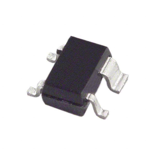
| 产品图片 |
|
| rohs | 符合RoHS无铅 / 符合限制有害物质指令(RoHS)规范要求 |
| 产品系列 | 电源管理 IC,监控电路,Maxim Integrated DS1818R-20+T&REconoReset |
| NumberofInputsMonitored | 1 Input |
| 数据手册 | |
| 产品型号 | DS1818R-20+T&R |
| 产品培训模块 | http://www.digikey.cn/PTM/IndividualPTM.page?site=cn&lang=zhs&ptm=25703http://www.digikey.cn/PTM/IndividualPTM.page?site=cn&lang=zhs&ptm=25705 |
| 产品种类 | 监控电路 |
| 人工复位 | Manual Reset |
| 供应商器件封装 | SOT-23-3 |
| 其它名称 | DS1818R-20+T&R-ND |
| 功率失效检测 | Yes |
| 包装 | 带卷 (TR) |
| 受监控电压数 | 1 |
| 商标 | Maxim Integrated |
| 复位 | 低有效 |
| 复位超时 | 最小为 100 ms |
| 安装类型 | 表面贴装 |
| 封装 | Reel |
| 封装/外壳 | TO-236-3,SC-59,SOT-23-3 |
| 封装/箱体 | TO-92-3 |
| 工作温度 | -40°C ~ 85°C |
| 工作电源电流 | 35 uA |
| 工厂包装数量 | 3000 |
| 最大工作温度 | + 85 C |
| 最小工作温度 | - 40 C |
| 标准包装 | 3,000 |
| 欠电压阈值 | 2.47 V |
| 电压-阈值 | 2.55V |
| 电池备用开关 | No Backup |
| 电源电压-最大 | 5.5 V |
| 电源电压-最小 | 1 V |
| 监视器 | No Watchdog |
| 类型 | 简单复位/加电复位 |
| 系列 | DS1818R |
| 芯片启用信号 | No Chip Enable |
| 被监测输入数 | 1 Input |
| 输出 | 开路漏极或开路集电极 |
| 输出类型 | Active Low, Open Drain |
| 过电压阈值 | 2.64 V |
| 重置延迟时间 | 250 ms |
| 阈值电压 | 1 V to 5.5 V |
| 零件号别名 | 90-1818R+020 DS1818R |


PDF Datasheet 数据手册内容提取
DS1818 3.3V EconoReset with Pushbutton BENEFITS AND FEATURES PIN ASSIGNMENT • Improves Reliability of Processor Operation Temperature-Compensated Voltage 3 o DALLAS Monitor for Precise, Automated Power- DS1818 Econo Fail Detection Reset Automatically Restarts a Microprocessor o After Power Failure 1 2 Maintains Reset for 150ms After V o CC TOP VIEW Returns to Tolerance for Processor SOT-23 PACKAGE See Mech. Stabilization Drawings Section On Website o Monitors Pushbutton for External 1 2 3 Override Active-Low Reset Output 1 2 3 o • Efficient Open-Drain Output with Internal BOTTOM VIEW 5.5kΩ Pullup Resistor Saves Power and Space TO-92 PACKAGE See Mech. 35µA (max) Quiescent Current Drawings Section o On Website • Allows for Easy Design with No Complicated Settings PIN DESCRIPTION Fixed 3.3V Reset Threshold o TO-92 5%, 10%, and 20% Tolerance Versions o Available 1 RST Active Low Reset Output 2 V Power Supply • Operates in Most Commercial and Industrial CC 3 GND Ground Environments -40°C to +85°C Operating Temperature o SOT-23 Range 1 RST Active Low Reset Output • MXD1818 Offers Improved Performance over 2 V Power Supply CC the DS1818 3 GND Ground DESCRIPTION The DS1818 EconoReset uses a precision temperature-compensated reference and comparator circuit to monitor the status of the power supply (V ). When an out-of-tolerance condition is detected, an internal CC power-fail signal is generated which forces reset to the active state. When V returns to an in-tolerance CC condition, the reset signal is kept in the active state for approximately 150 ms to allow the power supply and processor to stabilize. The DS1818 also monitors a pushbutton on the reset output. If the reset line is pulled low, a reset is generated upon release and the DS1818 output will be held in reset output low for typically 150 ms. 1 of 5 19-7559; Rev 1; 3/15
DS1818 OPERATION - POWER MONITOR The DS1818 provides the functions of detecting out-of-tolerance power supply conditions and warning a processor-based system of impending power failures. When VCC is detected as out-of-tolerance, the RST signal is asserted. On power-up, RST is kept active for approximately 150 ms after the power supply has reached the selected tolerance. This allows the power supply and microprocessor to stabilize before RST is released. BLOCK DIAGRAM (OPEN-DRAIN OUTPUT) Figure 1 APPLICATION EXAMPLE Figure 2 OPERATION - PUSHBUTTON RESET The DS1818 provides a pushbutton switch for manual reset control. When the DS1818 is not in a reset cycle, a pushbutton reset can be generated by pulling the RST pin low for at least 1 µs. When the pushbutton is held low, the RST is forced active low and will remain active low for about 150 ms after the pushbutton is released. See Figure 2 for an application example and Figure 3 for the timing diagram. TIMING DIAGRAM: PUSHBUTTON RESET Figure 3 2 of 6
DS1818 TIMING DIAGRAM: POWER-UP Figure 4 TIMING DIAGRAM: POWER-DOWN Figure 5 3 of 6
DS1818 ABSOLUTE MAXIMUM RATINGS* Voltage on V Pin Relative to Ground -0.5V to +7.0V CC Voltage on RST Relative to Ground -0.5V to +5VCC +0.5V Operating Temperature -40°C to +85°C Storage Temperature -55°C to +125°C Soldering Temperature 260°C for 10 seconds * This is a stress rating only and functional operation of the device at these or any other conditions above those indicated in the operation sections of this specification is not implied. Exposure to absolute maximum rating conditions for extended periods of time may affect reliability. RECOMMENDED DC OPERATING CONDITIONS (-40°C to +85°C) PARAMETER SYMBOL MIN TYP MAX UNITS NOTES Supply Voltage V 1.0 5.5 V 1 CC DC ELECTRICAL CHARACTERISTICS (-40°C to +85°C; V =1.2V to 5.5V) CC PARAMETER SYMBOL MIN TYP MAX UNITS NOTES Output Current @ 0.4 V I +10 mA 2, 3 OL Voltage Input Low V 0.4 V 1 IL Voltage Input High V 0.7 V 1 IH *V CC Operating Current V < 5.5V I 28 35 µA 4 CC CC V Trip Point (DS1818-5) V 2.98 3.06 3.15 V 1 CC CCTP V Trip Point (DS1818-10) V 2.80 2.88 2.97 V 1 CC CCTP V Trip Point (DS1818-20) V 2.47 2.55 2.64 V 1 CC CCTP Internal Pull-up Resistor R 3.50 5.5 7.5 kΩ 7 P Output Capacitance C 10 pF OUT AC ELECTRICAL CHARACTERISTICS (-40°C to +85°C; V =1.2V to 5.5V) CC PARAMETER SYMBOL MIN TYP MAX UNITS NOTES RESET Active Time t 100 150 250 ms 5 RST VCC Detect to RST tRPD 2 5 µs V Slew Rate t 300 µs 8 CC F (V (MAX) to V (MIN)) CCTP CCTP V Slew Rate t 0 ns CC R (V (MIN) to V (MAX)) CCTP CCTP t 100 150 250 ms 5, 6 VCC Detect to RST RPU Pushbutton Detect to RST tPB 1 µs Pushbutton Reset t 100 150 250 ms 5 PBRST 4 of 6
DS1818 NOTES: 1. All voltages are referenced to ground. 2. Measured with V ≥ 2.7V. CC 3. A 1 kΩ external pull-up resistor may be required in some applications for proper operation of the microprocessor reset control circuit. 4. Measured with RST output open. 5. Measured with 2.7V ≤ V ≤ 3.3V. CC 6. t = 5 µs. R 7. V and I are a function of the value of R and the associated output load conditions. OH OH P 8. The t value is for reference in defining values for t and should not be considered a requirement for F RPD proper operation or use of the device. PART MARKING CODES “A”, “B”, &“C” represent the device type. “D” represents the device tolerance. 810 - DS1810 A - 5% 811 - DS1811 B - 10% 812 - DS1812 C - 15% 813 - DS1813 D - 20% 815 - DS1815 816 - DS1816 817 - DS1817 818 - DS1818 5 of 6
DS1818 REVISION HISTORY REVISION REVISION PAGES DESCRIPTION NUMBER DATE CHANGED 1 3/15 Updated Benefits and Features section 1 For pricing, delivery, and ordering information, please contact Maxim Direct at 1-888-629-4642, or visit Maxim Integrated’s website at www.maximintegrated.com. Maxim Integrated cannot assume responsibility for use of any circuitry other than circuitry entirely embodied in a Maxim Integrated product. No circuit patent licenses are implied. Maxim Integrated reserves the right to change the circuitry and specifications without notice at any time. The parametric values (min and max limits) shown in the Electrical Characteristics table are guaranteed. Other parametric values quoted in this data sheet are provided for guidance. Maxim Integrated and the Maxim Integrated logo are trademarks of Maxim Integrated Products, Inc. © 2015 Maxim Integrated Products, Inc. 6 of 6
Mouser Electronics Authorized Distributor Click to View Pricing, Inventory, Delivery & Lifecycle Information: M axim Integrated: DS1818-10 DS1818-10+T&R DS1818-20 DS1818-20+ DS1818-20+T&R DS1818-5+T&R DS1818R-10+T&R DS1818R-20+T&R DS1818R-5+T&R DS1818-5 DS1818-10+ DS1818-5+ DS1818R-5-U