ICGOO在线商城 > 集成电路(IC) > 嵌入式 - 微控制器 > STM32F100C6T6B
 Datasheet下载
- 型号: STM32F100C6T6B
- 制造商: STMicroelectronics
- 库位|库存: xxxx|xxxx
- 要求:
| 数量阶梯 | 香港交货 | 国内含税 |
| +xxxx | $xxxx | ¥xxxx |
查看当月历史价格
查看今年历史价格
STM32F100C6T6B产品简介:
ICGOO电子元器件商城为您提供STM32F100C6T6B由STMicroelectronics设计生产,在icgoo商城现货销售,并且可以通过原厂、代理商等渠道进行代购。 STM32F100C6T6B价格参考。STMicroelectronicsSTM32F100C6T6B封装/规格:嵌入式 - 微控制器, ARM® Cortex®-M3 微控制器 IC STM32F1 32-位 24MHz 32KB(32K x 8) 闪存 。您可以下载STM32F100C6T6B参考资料、Datasheet数据手册功能说明书,资料中有STM32F100C6T6B 详细功能的应用电路图电压和使用方法及教程。
STM32F100C6T6B是STMicroelectronics(意法半导体)推出的一款基于ARM Cortex-M3内核的32位微控制器,属于STM32F1系列。该型号具备低功耗、高集成度和丰富的外设资源,适用于多种嵌入式应用场景。

 1. 工业控制
STM32F100C6T6B广泛应用于工业自动化领域,如电机控制、传感器数据采集与处理等。其内置的定时器、PWM(脉宽调制)功能以及ADC(模数转换器)使其能够精确控制电机的速度和位置,同时实时监测环境参数,如温度、湿度等。此外,它还支持多种通信接口(如UART、SPI、I2C),便于与其他设备或系统进行数据交换,满足工业网络化需求。

 2. 消费电子
在消费电子产品中,STM32F100C6T6B可用于智能家电、便携式设备等。例如,在智能家居系统中,它可以作为中央控制器,管理灯光、温控、安防等功能;在便携式医疗设备中,它能处理心率、血压等生理信号,并通过蓝牙或其他无线通信模块将数据传输到手机或云端。

 3. 物联网(IoT)
随着物联网技术的发展,STM32F100C6T6B凭借其低功耗特性和强大的处理能力,成为理想的物联网节点控制器。它可以通过Wi-Fi、Zigbee、LoRa等无线通信协议连接到互联网,实现远程监控和管理。同时,其丰富的GPIO(通用输入输出)引脚可以方便地连接各种传感器和执行器,构建智能化的感知和控制系统。

 4. 家用电器
该微控制器也适用于家用电器的设计,如洗衣机、空调、冰箱等。它可以优化家电的工作模式,提高能源利用效率,降低能耗。通过内置的RTC(实时时钟)和低功耗管理模式,STM32F100C6T6B能够在待机状态下保持长时间运行,延长电池寿命。

总之,STM32F100C6T6B以其卓越的性能、灵活的配置和广泛的适用性,成为众多嵌入式应用的理想选择。
| 参数 | 数值 |
| A/D位大小 | 12 bit |
| 产品目录 | 集成电路 (IC)半导体 |
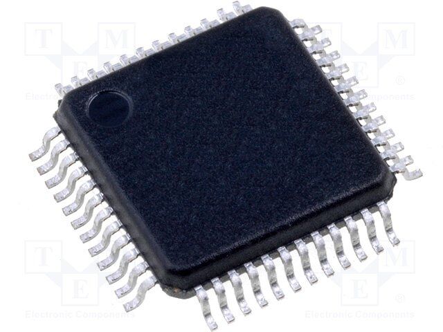
| 描述 | MCU 32BIT ARM 32K FLASH 48LQFPARM微控制器 - MCU 32BIT CORTEX M3 48PINS 32KB |
| EEPROM容量 | - |
| 产品分类 | |
| I/O数 | 37 |
| 品牌 | STMicroelectronics |
| 产品手册 | |
| 产品图片 |
|
| rohs | 符合RoHS无铅 / 符合限制有害物质指令(RoHS)规范要求 |
| 产品系列 | 嵌入式处理器和控制器,微控制器 - MCU,ARM微控制器 - MCU,STMicroelectronics STM32F100C6T6BSTM32 F1 |
| 数据手册 | |
| 产品型号 | STM32F100C6T6B |
| RAM容量 | 4K x 8 |
| 产品培训模块 | http://www.digikey.cn/PTM/IndividualPTM.page?site=cn&lang=zhs&ptm=30015http://www.digikey.cn/PTM/IndividualPTM.page?site=cn&lang=zhs&ptm=30339 |
| 产品种类 | ARM微控制器 - MCU |
| 供应商器件封装 | * |
| 其它名称 | 497-10500 |
| 其它有关文件 | http://www.st.com/web/catalog/mmc/FM141/SC1169/SS1031/LN775/PF216838?referrer=70071840 |
| 包装 | 托盘 |
| 可用A/D通道 | 10 |
| 可编程输入/输出端数量 | 37 |
| 商标 | STMicroelectronics |
| 商标名 | STM32 |
| 处理器系列 | ARM Cortex-M |
| 外设 | DMA,PDR,POR,PVD,PWM,温度传感器,WDT |
| 安装风格 | SMD/SMT |
| 定时器数量 | 5 Timer |
| 封装 | Tray |
| 封装/外壳 | 48-LQFP |
| 封装/箱体 | LQFP-48 |
| 工作温度 | -40°C ~ 85°C |
| 工作电源电压 | 2 V to 3.6 V |
| 工厂包装数量 | 250 |
| 振荡器类型 | 内部 |
| 接口类型 | I2C, SPI, USART |
| 数据RAM大小 | 4 kB |
| 数据Ram类型 | SRAM |
| 数据总线宽度 | 32 bit |
| 数据转换器 | A/D 10x12b; D/A 2x12b |
| 最大工作温度 | + 85 C |
| 最大时钟频率 | 24 MHz |
| 最小工作温度 | - 40 C |
| 标准包装 | 250 |
| 核心 | ARM Cortex M3 |
| 核心处理器 | ARM® Cortex™-M3 |
| 核心尺寸 | 32-位 |
| 片上ADC | Yes |
| 特色产品 | http://www.digikey.com/product-highlights/cn/zh/stmicroelectronics-stm32/1369 |
| 电压-电源(Vcc/Vdd) | 2 V ~ 3.6 V |
| 程序存储器大小 | 32 kB |
| 程序存储器类型 | Flash |
| 程序存储容量 | 32KB(32K x 8) |
| 系列 | STM32F1 |
| 输入/输出端数量 | 37 I/O |
| 连接性 | I²C, IrDA, LIN, SPI, UART/USART |
| 速度 | 24MHz |
| 配用 | /product-detail/zh/STM32100B-MCKIT/497-12818-ND/2776522/product-detail/zh/STM32100B-EVAL/STM32100B-EVAL-ND/2529300 |


- 商务部:美国ITC正式对集成电路等产品启动337调查
- 曝三星4nm工艺存在良率问题 高通将骁龙8 Gen1或转产台积电
- 太阳诱电将投资9.5亿元在常州建新厂生产MLCC 预计2023年完工
- 英特尔发布欧洲新工厂建设计划 深化IDM 2.0 战略
- 台积电先进制程称霸业界 有大客户加持明年业绩稳了
- 达到5530亿美元!SIA预计今年全球半导体销售额将创下新高
- 英特尔拟将自动驾驶子公司Mobileye上市 估值或超500亿美元
- 三星加码芯片和SET,合并消费电子和移动部门,撤换高东真等 CEO
- 三星电子宣布重大人事变动 还合并消费电子和移动部门
- 海关总署:前11个月进口集成电路产品价值2.52万亿元 增长14.8%


PDF Datasheet 数据手册内容提取
STM32F100x4 STM32F100x6 STM32F100x8 STM32F100xB ® Low & medium-density value line, advanced ARM -based 32-bit MCU with 16 to 128 KB Flash, 12 timers, ADC, DAC & 8 comm interfaces Datasheet - production data Features (cid:41)(cid:37)(cid:42)(cid:36) • Core: ARM® 32-bit Cortex®-M3 CPU – 24 MHz maximum frequency, 1.25 DMIPS/MHz (Dhrystone 2.1) LQFP100 14 × 14 mm performance LQFP64 10 × 10 mm TFBGA64 5 × 5 mm LQFP48 7 × 7 mm – Single-cycle multiplication and hardware division • Up to 12 timers • Memories – Up to three 16-bit timers, each with up to 4 IC/OC/PWM or pulse counter – 16 to 128 Kbytes of Flash memory – 16-bit, 6-channel advanced-control timer: – 4 to 8 Kbytes of SRAM up to 6 channels for PWM output, dead • Clock, reset and supply management time generation and emergency stop – 2.0 to 3.6 V application supply and I/Os – One 16-bit timer, with 2 IC/OC, 1 – POR, PDR and programmable voltage OCN/PWM, dead-time generation and detector (PVD) emergency stop – 4-to-24 MHz crystal oscillator – Two 16-bit timers, each with – Internal 8 MHz factory-trimmed RC IC/OC/OCN/PWM, dead-time generation and emergency stop – Internal 40 kHz RC – 2 watchdog timers (Independent and – PLL for CPU clock Window) – 32 kHz oscillator for RTC with calibration – SysTick timer: 24-bit downcounter • Low power – Two 16-bit basic timers to drive the DAC – Sleep, Stop and Standby modes • Up to 8 communications interfaces – V supply for RTC and backup registers BAT – Up to two I2C interfaces (SMBus/PMBus) • Debug mode – Up to 3 USARTs (ISO 7816 interface, LIN, – Serial wire debug (SWD) and JTAG IrDA capability, modem control) interfaces – Up to 2 SPIs (12 Mbit/s) • DMA – Consumer electronics control (CEC) – 7-channel DMA controller interface – Peripherals supported: timers, ADC, SPIs, • CRC calculation unit, 96-bit unique ID I2Cs, USARTs and DACs • ECOPACK® packages • 1 × 12-bit, 1.2 µs A/D converter (up to 16 channels) Table 1. Device summary – Conversion range: 0 to 3.6 V Reference Part number – Temperature sensor • 2 × 12-bit D/A converters STM32F100x4 STM32F100C4, STM32F100R4 • Up to 80 fast I/O ports STM32F100x6 STM32F100C6, STM32F100R6 – 37/51/80 I/Os, all mappable on 16 external STM32F100C8, STM32F100R8, STM32F100x8 interrupt vectors and almost all 5 V-tolerant STM32F100V8 STM32F100CB, STM32F100RB, STM32F100xB STM32F100VB November 2016 DocID16455 Rev 9 1/96 This is information on a product in full production. www.st.com
Contents STM32F100x4, STM32F100x6, STM32F100x8, STM32F100xB Contents 1 Introduction . . . . . . . . . . . . . . . . . . . . . . . . . . . . . . . . . . . . . . . . . . . . . . . . 9 2 Description . . . . . . . . . . . . . . . . . . . . . . . . . . . . . . . . . . . . . . . . . . . . . . . . 10 2.1 Device overview . . . . . . . . . . . . . . . . . . . . . . . . . . . . . . . . . . . . . . . . . . . . .11 2.2 Overview . . . . . . . . . . . . . . . . . . . . . . . . . . . . . . . . . . . . . . . . . . . . . . . . . 14 2.2.1 ARM® Cortex®-M3 core with embedded Flash and SRAM . . . . . . . . . . 14 2.2.2 Embedded Flash memory . . . . . . . . . . . . . . . . . . . . . . . . . . . . . . . . . . . 14 2.2.3 CRC (cyclic redundancy check) calculation unit . . . . . . . . . . . . . . . . . . 14 2.2.4 Embedded SRAM . . . . . . . . . . . . . . . . . . . . . . . . . . . . . . . . . . . . . . . . . 14 2.2.5 Nested vectored interrupt controller (NVIC) . . . . . . . . . . . . . . . . . . . . . . 14 2.2.6 External interrupt/event controller (EXTI) . . . . . . . . . . . . . . . . . . . . . . . 15 2.2.7 Clocks and startup . . . . . . . . . . . . . . . . . . . . . . . . . . . . . . . . . . . . . . . . . 15 2.2.8 Boot modes . . . . . . . . . . . . . . . . . . . . . . . . . . . . . . . . . . . . . . . . . . . . . . 15 2.2.9 Power supply schemes . . . . . . . . . . . . . . . . . . . . . . . . . . . . . . . . . . . . . 15 2.2.10 Power supply supervisor . . . . . . . . . . . . . . . . . . . . . . . . . . . . . . . . . . . . 15 2.2.11 Voltage regulator . . . . . . . . . . . . . . . . . . . . . . . . . . . . . . . . . . . . . . . . . . 16 2.2.12 Low-power modes . . . . . . . . . . . . . . . . . . . . . . . . . . . . . . . . . . . . . . . . . 16 2.2.13 DMA . . . . . . . . . . . . . . . . . . . . . . . . . . . . . . . . . . . . . . . . . . . . . . . . . . . . 16 2.2.14 RTC (real-time clock) and backup registers . . . . . . . . . . . . . . . . . . . . . . 17 2.2.15 Timers and watchdogs . . . . . . . . . . . . . . . . . . . . . . . . . . . . . . . . . . . . . . 17 2.2.16 I²C bus . . . . . . . . . . . . . . . . . . . . . . . . . . . . . . . . . . . . . . . . . . . . . . . . . . 19 2.2.17 Universal synchronous/asynchronous receiver transmitter (USART) . . 19 2.2.18 Serial peripheral interface (SPI) . . . . . . . . . . . . . . . . . . . . . . . . . . . . . . . 20 2.2.19 HDMI (high-definition multimedia interface) consumer electronics control (CEC) . . . . . . . . . . . . . . . . . . . . . . . . . . . . . . . . . . . . 20 2.2.20 GPIOs (general-purpose inputs/outputs) . . . . . . . . . . . . . . . . . . . . . . . . 20 2.2.21 Remap capability . . . . . . . . . . . . . . . . . . . . . . . . . . . . . . . . . . . . . . . . . . 20 2.2.22 ADC (analog-to-digital converter) . . . . . . . . . . . . . . . . . . . . . . . . . . . . . 20 2.2.23 DAC (digital-to-analog converter) . . . . . . . . . . . . . . . . . . . . . . . . . . . . . 21 2.2.24 Temperature sensor . . . . . . . . . . . . . . . . . . . . . . . . . . . . . . . . . . . . . . . . 21 2.2.25 Serial wire JTAG debug port (SWJ-DP) . . . . . . . . . . . . . . . . . . . . . . . . . 21 3 Pinouts and pin description . . . . . . . . . . . . . . . . . . . . . . . . . . . . . . . . . . 22 4 Memory mapping . . . . . . . . . . . . . . . . . . . . . . . . . . . . . . . . . . . . . . . . . . . 30 2/96 DocID16455 Rev 9
STM32F100x4, STM32F100x6, STM32F100x8, STM32F100xB Contents 5 Electrical characteristics . . . . . . . . . . . . . . . . . . . . . . . . . . . . . . . . . . . . 31 5.1 Parameter conditions . . . . . . . . . . . . . . . . . . . . . . . . . . . . . . . . . . . . . . . . 31 5.1.1 Minimum and maximum values . . . . . . . . . . . . . . . . . . . . . . . . . . . . . . . 31 5.1.2 Typical values . . . . . . . . . . . . . . . . . . . . . . . . . . . . . . . . . . . . . . . . . . . . 31 5.1.3 Typical curves . . . . . . . . . . . . . . . . . . . . . . . . . . . . . . . . . . . . . . . . . . . . 31 5.1.4 Loading capacitor . . . . . . . . . . . . . . . . . . . . . . . . . . . . . . . . . . . . . . . . . 31 5.1.5 Pin input voltage . . . . . . . . . . . . . . . . . . . . . . . . . . . . . . . . . . . . . . . . . . 31 5.1.6 Power supply scheme . . . . . . . . . . . . . . . . . . . . . . . . . . . . . . . . . . . . . . 32 5.1.7 Current consumption measurement . . . . . . . . . . . . . . . . . . . . . . . . . . . 33 5.2 Absolute maximum ratings . . . . . . . . . . . . . . . . . . . . . . . . . . . . . . . . . . . . 33 5.3 Operating conditions . . . . . . . . . . . . . . . . . . . . . . . . . . . . . . . . . . . . . . . . 34 5.3.1 General operating conditions . . . . . . . . . . . . . . . . . . . . . . . . . . . . . . . . . 34 5.3.2 Operating conditions at power-up / power-down . . . . . . . . . . . . . . . . . . 35 5.3.3 Embedded reset and power control block characteristics . . . . . . . . . . . 35 5.3.4 Embedded reference voltage . . . . . . . . . . . . . . . . . . . . . . . . . . . . . . . . . 37 5.3.5 Supply current characteristics . . . . . . . . . . . . . . . . . . . . . . . . . . . . . . . . 37 5.3.6 External clock source characteristics . . . . . . . . . . . . . . . . . . . . . . . . . . . 46 5.3.7 Internal clock source characteristics . . . . . . . . . . . . . . . . . . . . . . . . . . . 50 5.3.8 PLL characteristics . . . . . . . . . . . . . . . . . . . . . . . . . . . . . . . . . . . . . . . . 52 5.3.9 Memory characteristics . . . . . . . . . . . . . . . . . . . . . . . . . . . . . . . . . . . . . 53 5.3.10 EMC characteristics . . . . . . . . . . . . . . . . . . . . . . . . . . . . . . . . . . . . . . . . 54 5.3.11 Absolute maximum ratings (electrical sensitivity) . . . . . . . . . . . . . . . . . 55 5.3.12 I/O current injection characteristics . . . . . . . . . . . . . . . . . . . . . . . . . . . . 56 5.3.13 I/O port characteristics . . . . . . . . . . . . . . . . . . . . . . . . . . . . . . . . . . . . . . 57 5.3.14 NRST pin characteristics . . . . . . . . . . . . . . . . . . . . . . . . . . . . . . . . . . . . 62 5.3.15 TIMx characteristics . . . . . . . . . . . . . . . . . . . . . . . . . . . . . . . . . . . . . . . . 63 5.3.16 Communications interfaces . . . . . . . . . . . . . . . . . . . . . . . . . . . . . . . . . . 64 5.3.17 12-bit ADC characteristics . . . . . . . . . . . . . . . . . . . . . . . . . . . . . . . . . . . 68 5.3.18 DAC electrical specifications . . . . . . . . . . . . . . . . . . . . . . . . . . . . . . . . . 73 5.3.19 Temperature sensor characteristics . . . . . . . . . . . . . . . . . . . . . . . . . . . . 75 6 Package information . . . . . . . . . . . . . . . . . . . . . . . . . . . . . . . . . . . . . . . . 76 6.1 LQFP100 package information . . . . . . . . . . . . . . . . . . . . . . . . . . . . . . . . . 76 6.2 LQFP64 package information . . . . . . . . . . . . . . . . . . . . . . . . . . . . . . . . . . 80 6.3 TFBGA64 package information . . . . . . . . . . . . . . . . . . . . . . . . . . . . . . . . 83 6.4 LQFP48 package information . . . . . . . . . . . . . . . . . . . . . . . . . . . . . . . . . . 86 DocID16455 Rev 9 3/96 4
Contents STM32F100x4, STM32F100x6, STM32F100x8, STM32F100xB 6.5 Thermal characteristics . . . . . . . . . . . . . . . . . . . . . . . . . . . . . . . . . . . . . . 89 6.5.1 Reference document . . . . . . . . . . . . . . . . . . . . . . . . . . . . . . . . . . . . . . . 89 6.5.2 Selecting the product temperature range . . . . . . . . . . . . . . . . . . . . . . . 90 7 Ordering information scheme . . . . . . . . . . . . . . . . . . . . . . . . . . . . . . . . 92 8 Revision history . . . . . . . . . . . . . . . . . . . . . . . . . . . . . . . . . . . . . . . . . . . 93 4/96 DocID16455 Rev 9
STM32F100x4, STM32F100x6, STM32F100x8, STM32F100xB List of tables List of tables Table 1. Device summary. . . . . . . . . . . . . . . . . . . . . . . . . . . . . . . . . . . . . . . . . . . . . . . . . . . . . . . . . . 1 Table 2. STM32F100xx features and peripheral counts. . . . . . . . . . . . . . . . . . . . . . . . . . . . . . . . . . 11 Table 3. Timer feature comparison. . . . . . . . . . . . . . . . . . . . . . . . . . . . . . . . . . . . . . . . . . . . . . . . . . 17 Table 4. Low & medium-density STM32F100xx pin definitions . . . . . . . . . . . . . . . . . . . . . . . . . . . . 24 Table 5. Voltage characteristics . . . . . . . . . . . . . . . . . . . . . . . . . . . . . . . . . . . . . . . . . . . . . . . . . . . . 33 Table 6. Current characteristics . . . . . . . . . . . . . . . . . . . . . . . . . . . . . . . . . . . . . . . . . . . . . . . . . . . . 34 Table 7. Thermal characteristics. . . . . . . . . . . . . . . . . . . . . . . . . . . . . . . . . . . . . . . . . . . . . . . . . . . . 34 Table 8. General operating conditions . . . . . . . . . . . . . . . . . . . . . . . . . . . . . . . . . . . . . . . . . . . . . . . 34 Table 9. Operating conditions at power-up / power-down . . . . . . . . . . . . . . . . . . . . . . . . . . . . . . . . 35 Table 10. Embedded reset and power control block characteristics. . . . . . . . . . . . . . . . . . . . . . . . . . 36 Table 11. Embedded internal reference voltage. . . . . . . . . . . . . . . . . . . . . . . . . . . . . . . . . . . . . . . . . 37 Table 12. Maximum current consumption in Run mode, code with data processing running from Flash . . . . . . . . . . . . . . . . . . . . . . . . . . . . . . . . . . . . . . . . . . . . . . . . . . . . . . . 38 Table 13. Maximum current consumption in Run mode, code with data processing running from RAM. . . . . . . . . . . . . . . . . . . . . . . . . . . . . . . . . . . . . . . . . . . . . . . . . . . . . . . . 38 Table 14. Maximum current consumption in Sleep mode, code running from Flash or RAM. . . . . . . 39 Table 15. Typical and maximum current consumptions in Stop and Standby modes . . . . . . . . . . . . 40 Table 16. Typical current consumption in Run mode, code with data processing running from Flash . . . . . . . . . . . . . . . . . . . . . . . . . . . . . . . . . . . . . . . . . . . . . . . . . . . . . . . 43 Table 17. Typical current consumption in Sleep mode, code running from Flash or RAM. . . . . . . . . 44 Table 18. Peripheral current consumption . . . . . . . . . . . . . . . . . . . . . . . . . . . . . . . . . . . . . . . . . . . . . 45 Table 19. High-speed external user clock characteristics. . . . . . . . . . . . . . . . . . . . . . . . . . . . . . . . . . 46 Table 20. Low-speed external user clock characteristics. . . . . . . . . . . . . . . . . . . . . . . . . . . . . . . . . . 47 Table 21. HSE 4-24 MHz oscillator characteristics. . . . . . . . . . . . . . . . . . . . . . . . . . . . . . . . . . . . . . . 48 Table 22. LSE oscillator characteristics (f = 32.768 kHz) . . . . . . . . . . . . . . . . . . . . . . . . . . . . . . . 49 LSE Table 23. HSI oscillator characteristics. . . . . . . . . . . . . . . . . . . . . . . . . . . . . . . . . . . . . . . . . . . . . . . . 50 Table 24. LSI oscillator characteristics . . . . . . . . . . . . . . . . . . . . . . . . . . . . . . . . . . . . . . . . . . . . . . . 51 Table 25. Low-power mode wakeup timings . . . . . . . . . . . . . . . . . . . . . . . . . . . . . . . . . . . . . . . . . . . 51 Table 26. PLL characteristics. . . . . . . . . . . . . . . . . . . . . . . . . . . . . . . . . . . . . . . . . . . . . . . . . . . . . . . 52 Table 27. Flash memory characteristics. . . . . . . . . . . . . . . . . . . . . . . . . . . . . . . . . . . . . . . . . . . . . . . 53 Table 28. Flash memory endurance and data retention. . . . . . . . . . . . . . . . . . . . . . . . . . . . . . . . . . . 53 Table 29. EMS characteristics . . . . . . . . . . . . . . . . . . . . . . . . . . . . . . . . . . . . . . . . . . . . . . . . . . . . . . 54 Table 30. EMI characteristics. . . . . . . . . . . . . . . . . . . . . . . . . . . . . . . . . . . . . . . . . . . . . . . . . . . . . . . 55 Table 31. ESD absolute maximum ratings. . . . . . . . . . . . . . . . . . . . . . . . . . . . . . . . . . . . . . . . . . . . . 55 Table 32. Electrical sensitivities . . . . . . . . . . . . . . . . . . . . . . . . . . . . . . . . . . . . . . . . . . . . . . . . . . . . . 56 Table 33. I/O current injection susceptibility. . . . . . . . . . . . . . . . . . . . . . . . . . . . . . . . . . . . . . . . . . . . 56 Table 34. I/O static characteristics . . . . . . . . . . . . . . . . . . . . . . . . . . . . . . . . . . . . . . . . . . . . . . . . . . . 57 Table 35. Output voltage characteristics . . . . . . . . . . . . . . . . . . . . . . . . . . . . . . . . . . . . . . . . . . . . . . 60 Table 36. I/O AC characteristics. . . . . . . . . . . . . . . . . . . . . . . . . . . . . . . . . . . . . . . . . . . . . . . . . . . . . 61 Table 37. NRST pin characteristics . . . . . . . . . . . . . . . . . . . . . . . . . . . . . . . . . . . . . . . . . . . . . . . . . . 62 Table 38. TIMx characteristics . . . . . . . . . . . . . . . . . . . . . . . . . . . . . . . . . . . . . . . . . . . . . . . . . . . . . . 63 Table 39. I2C characteristics. . . . . . . . . . . . . . . . . . . . . . . . . . . . . . . . . . . . . . . . . . . . . . . . . . . . . . . . 64 Table 40. SCL frequency (f = 24 MHz, V = 3.3 V) . . . . . . . . . . . . . . . . . . . . . . . . . . . . . . . . . 65 PCLK1 DD Table 41. SPI characteristics . . . . . . . . . . . . . . . . . . . . . . . . . . . . . . . . . . . . . . . . . . . . . . . . . . . . . . . 66 Table 42. ADC characteristics . . . . . . . . . . . . . . . . . . . . . . . . . . . . . . . . . . . . . . . . . . . . . . . . . . . . . . 69 Table 43. R max for f = 12 MHz. . . . . . . . . . . . . . . . . . . . . . . . . . . . . . . . . . . . . . . . . . . . . . . . 70 AIN ADC Table 44. ADC accuracy - limited test conditions. . . . . . . . . . . . . . . . . . . . . . . . . . . . . . . . . . . . . . . . 70 Table 45. ADC accuracy . . . . . . . . . . . . . . . . . . . . . . . . . . . . . . . . . . . . . . . . . . . . . . . . . . . . . . . . . . 70 DocID16455 Rev 9 5/96 6
List of tables STM32F100x4, STM32F100x6, STM32F100x8, STM32F100xB Table 46. DAC characteristics . . . . . . . . . . . . . . . . . . . . . . . . . . . . . . . . . . . . . . . . . . . . . . . . . . . . . . 73 Table 47. TS characteristics. . . . . . . . . . . . . . . . . . . . . . . . . . . . . . . . . . . . . . . . . . . . . . . . . . . . . . . . 75 Table 48. LQPF100 - 100-pin, 14 x 14 mm low-profile quad flat package mechanical data . . . . . . . . . . . . . . . . . . . . . . . . . . . . . . . . . . . . . . . . . . . . . . . . . . . . . . . . . 77 Table 49. LQFP64 - 64-pin, 10 x 10 mm low-profile quad flat package mechanical data . . . . . . . . . . . . . . . . . . . . . . . . . . . . . . . . . . . . . . . . . . . . . . . . . . . . . . . . . 80 Table 50. TFBGA64 – 64-ball, 5 x 5 mm, 0.5 mm pitch, thin profile fine pitch ball grid array package mechanical data. . . . . . . . . . . . . . . . . . . . . . . . . . . . . . . . . . . . . . . . . . 83 Table 51. TFBGA64 recommended PCB design rules (0.5 mm pitch BGA). . . . . . . . . . . . . . . . . . . . 84 Table 52. LQFP48 - 48-pin, 7 x 7 mm low-profile quad flat package mechanical data . . . . . . . . . . . . . . . . . . . . . . . . . . . . . . . . . . . . . . . . . . . . . . . . . . . . . . . . . 86 Table 53. Package thermal characteristics. . . . . . . . . . . . . . . . . . . . . . . . . . . . . . . . . . . . . . . . . . . . . 89 Table 54. Ordering information scheme. . . . . . . . . . . . . . . . . . . . . . . . . . . . . . . . . . . . . . . . . . . . . . . 92 Table 55. Document revision history . . . . . . . . . . . . . . . . . . . . . . . . . . . . . . . . . . . . . . . . . . . . . . . . . 93 6/96 DocID16455 Rev 9
STM32F100x4, STM32F100x6, STM32F100x8, STM32F100xB List of figures List of figures Figure 1. STM32F100xx value line block diagram. . . . . . . . . . . . . . . . . . . . . . . . . . . . . . . . . . . . . . . 12 Figure 2. Clock tree . . . . . . . . . . . . . . . . . . . . . . . . . . . . . . . . . . . . . . . . . . . . . . . . . . . . . . . . . . . . . . 13 Figure 3. STM32F100xx value line LQFP100 pinout. . . . . . . . . . . . . . . . . . . . . . . . . . . . . . . . . . . . . 22 Figure 4. STM32F100xx value line LQFP64 pinout. . . . . . . . . . . . . . . . . . . . . . . . . . . . . . . . . . . . . . 23 Figure 5. STM32F100xx value line LQFP48 pinout. . . . . . . . . . . . . . . . . . . . . . . . . . . . . . . . . . . . . . 23 Figure 6. STM32F100xx value line TFBGA64 ballout . . . . . . . . . . . . . . . . . . . . . . . . . . . . . . . . . . . . 24 Figure 7. Memory map. . . . . . . . . . . . . . . . . . . . . . . . . . . . . . . . . . . . . . . . . . . . . . . . . . . . . . . . . . . . 30 Figure 8. Pin loading conditions. . . . . . . . . . . . . . . . . . . . . . . . . . . . . . . . . . . . . . . . . . . . . . . . . . . . . 32 Figure 9. Pin input voltage. . . . . . . . . . . . . . . . . . . . . . . . . . . . . . . . . . . . . . . . . . . . . . . . . . . . . . . . . 32 Figure 10. Power supply scheme. . . . . . . . . . . . . . . . . . . . . . . . . . . . . . . . . . . . . . . . . . . . . . . . . . . . . 32 Figure 11. Current consumption measurement scheme . . . . . . . . . . . . . . . . . . . . . . . . . . . . . . . . . . . 33 Figure 12. Maximum current consumption in Run mode versus frequency (at 3.6 V) - code with data processing running from RAM, peripherals enabled. . . . . . . . . . . . . . . . . . 39 Figure 13. Maximum current consumption in Run mode versus frequency (at 3.6 V) - code with data processing running from RAM, peripherals disabled . . . . . . . . . . . . . . . . . 39 Figure 14. Typical current consumption on V with RTC on vs. temperature BAT at different V values . . . . . . . . . . . . . . . . . . . . . . . . . . . . . . . . . . . . . . . . . . . . . . . . . . . 40 BAT Figure 15. Typical current consumption in Stop mode with regulator in Run mode versus temperature at V = 3.3 V and 3.6 V . . . . . . . . . . . . . . . . . . . . . . . . . . . . . . . . . . 41 DD Figure 16. Typical current consumption in Stop mode with regulator in Low-power mode versus temperature at V = 3.3 V and 3.6 V . . . . . . . . . . . . . . . . . . 41 DD Figure 17. Typical current consumption in Standby mode versus temperature at V = 3.3 V and 3.6 V . . . . . . . . . . . . . . . . . . . . . . . . . . . . . . . . . . 42 DD Figure 18. High-speed external clock source AC timing diagram . . . . . . . . . . . . . . . . . . . . . . . . . . . . 46 Figure 19. Low-speed external clock source AC timing diagram. . . . . . . . . . . . . . . . . . . . . . . . . . . . . 47 Figure 20. Typical application with an 8 MHz crystal. . . . . . . . . . . . . . . . . . . . . . . . . . . . . . . . . . . . . . 48 Figure 21. Typical application with a 32.768 kHz crystal. . . . . . . . . . . . . . . . . . . . . . . . . . . . . . . . . . . 50 Figure 22. Standard I/O input characteristics - CMOS port. . . . . . . . . . . . . . . . . . . . . . . . . . . . . . . . . 58 Figure 23. Standard I/O input characteristics - TTL port . . . . . . . . . . . . . . . . . . . . . . . . . . . . . . . . . . . 58 Figure 24. 5 V tolerant I/O input characteristics - CMOS port . . . . . . . . . . . . . . . . . . . . . . . . . . . . . . . 59 Figure 25. 5 V tolerant I/O input characteristics - TTL port . . . . . . . . . . . . . . . . . . . . . . . . . . . . . . . . . 59 Figure 26. I/O AC characteristics definition . . . . . . . . . . . . . . . . . . . . . . . . . . . . . . . . . . . . . . . . . . . . . 62 Figure 27. Recommended NRST pin protection . . . . . . . . . . . . . . . . . . . . . . . . . . . . . . . . . . . . . . . . . 63 Figure 28. I2C bus AC waveforms and measurement circuit(1) . . . . . . . . . . . . . . . . . . . . . . . . . . . . . . 65 Figure 29. SPI timing diagram - slave mode and CPHA = 0 . . . . . . . . . . . . . . . . . . . . . . . . . . . . . . . . 67 Figure 30. SPI timing diagram - slave mode and CPHA = 1(1) . . . . . . . . . . . . . . . . . . . . . . . . . . . . . . 67 Figure 31. SPI timing diagram - master mode(1) . . . . . . . . . . . . . . . . . . . . . . . . . . . . . . . . . . . . . . . . . 68 Figure 32. ADC accuracy characteristics. . . . . . . . . . . . . . . . . . . . . . . . . . . . . . . . . . . . . . . . . . . . . . . 71 Figure 33. Typical connection diagram using the ADC . . . . . . . . . . . . . . . . . . . . . . . . . . . . . . . . . . . . 71 Figure 34. Power supply and reference decoupling (V not connected to V ). . . . . . . . . . . . . . 72 REF+ DDA Figure 35. Power supply and reference decoupling (V connected to V ). . . . . . . . . . . . . . . . . 72 REF+ DDA Figure 36. 12-bit buffered /non-buffered DAC . . . . . . . . . . . . . . . . . . . . . . . . . . . . . . . . . . . . . . . . . . . 74 Figure 37. LQFP100 - 100-pin, 14 x 14 mm low-profile quad flat package outline . . . . . . . . . . . . . . . 76 Figure 38. LQFP100 - 100-pin, 14 x 14 mm low-profile quad flat recommended footprint. . . . . . . . . . . . . . . . . . . . . . . . . . . . . . . . . . . . . . . . . . . . . . . . . . . . 78 Figure 39. LQFP100 marking example (package top view). . . . . . . . . . . . . . . . . . . . . . . . . . . . . . . . . 79 Figure 40. LQFP64 – 10 x 10 mm 64 pin low-profile quad flat package outline . . . . . . . . . . . . . . . . . 80 Figure 41. LQFP64 - 64-pin, 10 x 10 mm low-profile quad flat recommended footprint . . . . . . . . . . . 81 DocID16455 Rev 9 7/96 8
List of figures STM32F100x4, STM32F100x6, STM32F100x8, STM32F100xB Figure 42. LQFP64 marking example (package top view). . . . . . . . . . . . . . . . . . . . . . . . . . . . . . . . . . 82 Figure 43. TFBGA64 – 64-ball, 5 x 5 mm, 0.5 mm pitch thin profile fine pitch ball grid array package outline. . . . . . . . . . . . . . . . . . . . . . . . . . . . . . . . . . . . . . . . . . . . . . . . . . . . . . . . . . 83 Figure 44. TFBGA64 – 64-ball, 5 x 5 mm, 0.5 mm pitch, thin profile fine pitch ball grid array, recommended footprint . . . . . . . . . . . . . . . . . . . . . . . . . . . . . . . . . . . . . . . . . . . 84 Figure 45. TFBGA64 marking example (package top view) . . . . . . . . . . . . . . . . . . . . . . . . . . . . . . . . 85 Figure 46. LQFP48 - 48-pin, 7 x 7 mm low-profile quad flat package outline . . . . . . . . . . . . . . . . . . . 86 Figure 47. LQFP48 - 48-pin, 7 x 7 mm low-profile quad flat package recommended footprint. . . . . . . . . . . . . . . . . . . . . . . . . . . . . . . . . . . . . . . . . . . . . . . . . . . . 87 Figure 48. LQFP48 marking example (package top view). . . . . . . . . . . . . . . . . . . . . . . . . . . . . . . . . . 88 Figure 49. LQFP100 P max vs. T . . . . . . . . . . . . . . . . . . . . . . . . . . . . . . . . . . . . . . . . . . . . . . . . . . 91 D A 8/96 DocID16455 Rev 9
STM32F100x4, STM32F100x6, STM32F100x8, STM32F100xB Introduction 1 Introduction This datasheet provides the ordering information and mechanical device characteristics of the STM32F100x4, STM32F100x6, STM32F100x8 and STM32F100xB microcontrollers. In the rest of the document, the STM32F100x4 and STM32F100x6 are referred to as low- density devices while the STM32F100x8 and STM32F100xB are identified as medium- density devices. This STM32F100xx datasheet should be read in conjunction with the low- and medium- density STM32F100xx reference manual. For information on programming, erasing and protection of the internal Flash memory please refer to the STM32F100xx Flash programming manual. The reference and Flash programming manuals are both available from the STMicroelectronics website www.st.com. For information on the Cortex®-M3 core please refer to the Cortex®-M3 Technical Reference Manual, available from the www.arm.com website at the following address: http://infocenter.arm.com. DocID16455 Rev 9 9/96 95
Description STM32F100x4, STM32F100x6, STM32F100x8, STM32F100xB 2 Description The STM32F100x4, STM32F100x6, STM32F100x8 and STM32F100xB microcontrollers incorporate the high-performance ARM® Cortex®-M3 32-bit RISC core operating at a 24 MHz frequency, high-speed embedded memories (Flash memory up to 128 Kbytes and SRAM up to 8 Kbytes), and an extensive range of enhanced peripherals and I/Os connected to two APB buses. All devices offer standard communication interfaces (up to two I2Cs, two SPIs, one HDMI CEC, and up to three USARTs), one 12-bit ADC, two 12-bit DACs, up to six general-purpose 16-bit timers and an advanced-control PWM timer. The STM32F100xx low- and medium-density devices operate in the – 40 to + 85 °C and – 40 to + 105 °C temperature ranges, from a 2.0 to 3.6 V power supply. A comprehensive set of power-saving mode allows the design of low-power applications. These microcontrollers include devices in three different packages ranging from 48 pins to 100 pins. Depending on the device chosen, different sets of peripherals are included. These features make these microcontrollers suitable for a wide range of applications such as application control and user interfaces, medical and hand-held equipment, PC and gaming peripherals, GPS platforms, industrial applications, PLCs, inverters, printers, scanners, alarm systems, video intercoms, and HVACs. 10/96 DocID16455 Rev 9
STM32F100x4, STM32F100x6, STM32F100x8, STM32F100xB Description 2.1 Device overview The description below gives an overview of the complete range of peripherals proposed in this family. Figure 1 shows the general block diagram of the device family. Table 2. STM32F100xx features and peripheral counts Peripheral STM32F100Cx STM32F100Rx STM32F100Vx Flash - Kbytes 16 32 64 128 16 32 64 128 64 128 SRAM - Kbytes 4 4 8 8 4 4 8 8 8 8 Advanced-control 1 1 1 1 1 Timers General-purpose 5(1) 6 5(1) 6 6 SPI 1(2) 2 1(2) 2 2 Communication I2C 1(3) 2 1(3) 2 2 interfaces USART 2(4) 3 2(4) 3 3 CEC 1 12-bit synchronized ADC 1 1 1 number of channels 10 channels 16 channels 16 channels GPIOs 37 51 80 12-bit DAC 2 Number of channels 2 CPU frequency 24 MHz Operating voltage 2.0 to 3.6 V Ambient operating temperature: –40 to +85 °C /–40 to +105 °C (see Table 8) Operating temperatures Junction temperature: –40 to +125 °C (see Table 8) Packages LQFP48 LQFP64, TFBGA64 LQFP100 1. TIM4 not present. 2. SPI2 is not present. 3. I2C2 is not present. 4. USART3 is not present. DocID16455 Rev 9 11/96 95
Description STM32F100x4, STM32F100x6, STM32F100x8, STM32F100xB Figure 1. STM32F100xx value line block diagram (cid:52)(cid:50)(cid:33)(cid:35)(cid:37)(cid:35)(cid:44)(cid:43) (cid:52)(cid:50)(cid:33)(cid:35)(cid:37)(cid:36)(cid:65)(cid:83)(cid:59)(cid:16)(cid:0)(cid:33)(cid:26)(cid:19)(cid:38)(cid:61) (cid:42)(cid:52)(cid:33)(cid:39)(cid:0)(cid:6)(cid:0)(cid:51)(cid:55) (cid:80)(cid:66)(cid:85)(cid:83) (cid:52)(cid:67)(cid:82)(cid:79)(cid:65)(cid:78)(cid:67)(cid:84)(cid:69)(cid:82)(cid:79)(cid:76)(cid:76)(cid:69)(cid:82) (cid:54)(cid:36)(cid:36)(cid:17)(cid:24) (cid:54)(cid:79)(cid:76)(cid:84)(cid:48)(cid:65)(cid:79)(cid:71)(cid:87)(cid:69)(cid:0)(cid:69)(cid:82)(cid:82)(cid:69)(cid:71)(cid:14) (cid:54)(cid:36)(cid:36)(cid:29)(cid:0)(cid:18)(cid:14)(cid:16)(cid:0)(cid:54)(cid:0)(cid:84)(cid:79)(cid:0)(cid:19)(cid:14)(cid:22)(cid:0)(cid:54) (cid:42)(cid:42)(cid:52)(cid:52)(cid:45)(cid:35)(cid:43)(cid:51)(cid:15)(cid:15)(cid:46)(cid:51)(cid:51)(cid:42)(cid:55)(cid:55)(cid:65)(cid:42)(cid:52)(cid:83)(cid:42)(cid:52)(cid:35)(cid:36)(cid:50)(cid:52)(cid:0)(cid:36)(cid:33)(cid:44)(cid:41)(cid:51)(cid:47)(cid:36)(cid:47)(cid:43)(cid:38)(cid:52)(cid:41) (cid:35)(cid:70)(cid:79)(cid:77)(cid:82)(cid:65)(cid:84)(cid:88)(cid:69)(cid:88)(cid:26)(cid:0)(cid:13)(cid:18)(cid:45)(cid:20)(cid:19)(cid:0)(cid:45)(cid:0)(cid:35)(cid:40)(cid:48)(cid:90)(cid:53) (cid:36)(cid:66)(cid:85)(cid:83) (cid:41)(cid:66)(cid:85)(cid:83) (cid:79)(cid:66)(cid:76)(cid:38)(cid:76)(cid:65)(cid:83)(cid:72)(cid:73)(cid:78)(cid:84)(cid:69)(cid:82)(cid:70)(cid:65)(cid:67)(cid:69) (cid:51)(cid:38)(cid:50)(cid:76)(cid:65)(cid:33)(cid:83)(cid:45)(cid:19)(cid:72)(cid:18)(cid:0)(cid:0)(cid:17)(cid:0)(cid:66)(cid:18)(cid:24)(cid:73)(cid:84)(cid:0)(cid:43)(cid:34) (cid:50)(cid:48)(cid:69)(cid:47)(cid:83)(cid:69)(cid:50)(cid:84) (cid:32)(cid:83)(cid:19)(cid:85)(cid:54)(cid:14)(cid:51)(cid:80)(cid:19)(cid:36)(cid:69)(cid:85)(cid:0)(cid:54)(cid:36)(cid:82)(cid:80)(cid:86)(cid:0)(cid:80)(cid:19)(cid:84)(cid:73)(cid:79)(cid:83)(cid:76)(cid:19)(cid:89)(cid:73)(cid:0)(cid:79)(cid:17)(cid:0)(cid:78)(cid:14)(cid:24)(cid:0)(cid:54) (cid:46)(cid:54)(cid:50)(cid:51)(cid:51)(cid:51)(cid:52) (cid:46)(cid:54)(cid:39)(cid:41)(cid:48)(cid:35)(cid:0)(cid:36)(cid:45)(cid:33) (cid:51)(cid:89)(cid:83)(cid:84)(cid:69)(cid:77) (cid:34)(cid:85)(cid:83)(cid:0)(cid:77)(cid:65)(cid:84)(cid:82)(cid:73)(cid:88) (cid:24)(cid:0)(cid:43)(cid:34) (cid:32)(cid:50)(cid:54)(cid:50)(cid:36)(cid:35)(cid:35)(cid:36)(cid:0)(cid:0)(cid:44)(cid:40)(cid:33)(cid:51)(cid:51) (cid:41)(cid:78)(cid:84) (cid:32)(cid:54)(cid:48)(cid:36)(cid:47)(cid:36)(cid:50)(cid:33)(cid:48)(cid:0)(cid:15)(cid:54)(cid:0)(cid:48)(cid:36)(cid:36)(cid:50) (cid:54)(cid:54)(cid:51)(cid:36)(cid:51)(cid:36)(cid:33)(cid:33) (cid:32)(cid:54)(cid:36)(cid:36) (cid:23)(cid:0)(cid:67)(cid:72)(cid:65)(cid:78)(cid:78)(cid:69)(cid:76)(cid:83) (cid:47)(cid:51)(cid:35)(cid:63)(cid:41)(cid:46) (cid:56)(cid:52)(cid:33)(cid:44)(cid:0)(cid:47)(cid:51)(cid:35)(cid:0) (cid:47)(cid:51)(cid:35)(cid:63)(cid:47)(cid:53)(cid:52) (cid:48)(cid:44)(cid:44) (cid:20)(cid:13)(cid:18)(cid:20)(cid:0)(cid:45)(cid:40)(cid:90) (cid:50)(cid:69)(cid:83)(cid:69)(cid:84)(cid:0)(cid:6) (cid:48)(cid:35)(cid:44)(cid:43)(cid:17) (cid:41)(cid:55)(cid:36)(cid:39) (cid:20)(cid:0)(cid:45)(cid:40)(cid:90) (cid:67)(cid:67)(cid:79)(cid:76)(cid:78)(cid:79)(cid:84)(cid:67)(cid:82)(cid:75)(cid:79)(cid:76)(cid:0) (cid:48)(cid:40)(cid:38)(cid:35)(cid:35)(cid:35)(cid:44)(cid:44)(cid:44)(cid:43)(cid:43)(cid:43)(cid:18) (cid:0)(cid:51)(cid:73)(cid:78)(cid:84)(cid:84)(cid:65)(cid:69)(cid:78)(cid:82)(cid:68)(cid:70)(cid:65)(cid:66)(cid:67)(cid:89)(cid:69) (cid:54)(cid:34)(cid:33)(cid:52)(cid:0)(cid:29)(cid:0)(cid:17)(cid:14)(cid:24)(cid:54)(cid:0)(cid:84)(cid:79)(cid:0)(cid:19)(cid:14)(cid:22)(cid:54) (cid:48)(cid:33)(cid:24)(cid:16)(cid:59)(cid:17)(cid:0)(cid:33)(cid:21)(cid:38)(cid:26)(cid:16)(cid:61) (cid:39)(cid:48)(cid:37)(cid:55)(cid:41)(cid:47)(cid:56)(cid:43)(cid:0)(cid:52)(cid:80)(cid:53)(cid:14)(cid:79)(cid:41)(cid:48)(cid:52)(cid:82)(cid:84)(cid:0)(cid:33) (cid:34)(cid:0)(cid:26)(cid:0)(cid:38)(cid:29)(cid:18)(cid:77)(cid:65)(cid:88) (cid:50)(cid:52)(cid:35)(cid:56)(cid:52)(cid:33)(cid:44)(cid:34)(cid:32)(cid:0)(cid:19)(cid:65)(cid:18)(cid:54)(cid:67)(cid:75)(cid:34)(cid:75)(cid:85)(cid:40)(cid:33)(cid:80)(cid:52)(cid:90) (cid:47)(cid:47)(cid:51)(cid:51)(cid:35)(cid:35)(cid:19)(cid:19)(cid:18)(cid:18)(cid:63)(cid:63)(cid:41)(cid:47)(cid:46)(cid:53)(cid:52) (cid:48)(cid:34)(cid:59)(cid:17)(cid:21)(cid:26)(cid:16)(cid:61) (cid:39)(cid:48)(cid:41)(cid:47)(cid:0)(cid:80)(cid:79)(cid:82)(cid:84)(cid:0)(cid:34) (cid:33)(cid:40) (cid:33)(cid:55)(cid:53) (cid:82)(cid:69)(cid:71)(cid:73)(cid:83)(cid:84)(cid:69)(cid:82) (cid:52)(cid:8)(cid:33)(cid:33)(cid:44)(cid:45)(cid:33)(cid:48)(cid:50)(cid:37)(cid:45)(cid:50)(cid:0)(cid:47)(cid:13)(cid:50)(cid:53)(cid:52)(cid:52)(cid:35)(cid:9)(cid:0) (cid:34)(cid:65)(cid:67)(cid:75)(cid:85)(cid:80)(cid:0)(cid:73)(cid:78)(cid:84)(cid:69)(cid:82)(cid:70)(cid:65)(cid:67)(cid:69) (cid:48)(cid:35)(cid:59)(cid:17)(cid:21)(cid:26)(cid:16)(cid:61) (cid:39)(cid:48)(cid:41)(cid:47)(cid:0)(cid:80)(cid:79)(cid:82)(cid:84)(cid:0)(cid:35) (cid:48)(cid:36)(cid:59)(cid:17)(cid:21)(cid:26)(cid:16)(cid:61) (cid:39)(cid:48)(cid:41)(cid:47)(cid:0)(cid:80)(cid:79)(cid:82)(cid:84)(cid:0)(cid:36) (cid:33)(cid:33)(cid:40)(cid:48)(cid:34)(cid:34)(cid:18)(cid:18) (cid:33)(cid:33)(cid:40)(cid:48)(cid:34)(cid:34)(cid:17)(cid:18) (cid:52)(cid:41)(cid:45)(cid:18) (cid:20)(cid:65)(cid:20)(cid:0)(cid:83)(cid:0)(cid:67)(cid:67)(cid:0)(cid:72)(cid:33)(cid:72)(cid:65)(cid:65)(cid:38)(cid:78)(cid:78)(cid:78)(cid:78)(cid:69)(cid:69)(cid:76)(cid:76)(cid:83)(cid:83) (cid:52)(cid:41)(cid:45)(cid:19) (cid:65)(cid:83)(cid:0)(cid:33)(cid:38) (cid:48)(cid:37)(cid:59)(cid:17)(cid:21)(cid:26)(cid:16)(cid:61) (cid:39)(cid:48)(cid:41)(cid:47)(cid:0)(cid:80)(cid:79)(cid:82)(cid:84)(cid:0)(cid:37) (cid:18)(cid:0)(cid:67)(cid:72)(cid:65)(cid:78)(cid:78)(cid:69)(cid:76)(cid:83)(cid:12)(cid:0)(cid:17)(cid:0)(cid:67)(cid:79)(cid:77)(cid:80)(cid:76)(cid:14) (cid:40)(cid:90) (cid:52)(cid:41)(cid:45)(cid:20)(cid:8)(cid:17)(cid:9) (cid:20)(cid:65)(cid:0)(cid:83)(cid:67)(cid:0)(cid:72)(cid:33)(cid:65)(cid:38)(cid:78)(cid:78)(cid:69)(cid:76)(cid:83) (cid:67)(cid:65)(cid:72)(cid:83)(cid:65)(cid:0)(cid:33)(cid:78)(cid:38)(cid:78)(cid:69)(cid:76)(cid:0)(cid:65)(cid:78)(cid:68)(cid:0)(cid:34)(cid:43)(cid:41)(cid:46)(cid:0) (cid:52)(cid:41)(cid:45)(cid:17)(cid:21) (cid:18)(cid:20)(cid:0)(cid:45) (cid:53)(cid:51)(cid:33)(cid:50)(cid:52)(cid:18) (cid:50)(cid:35)(cid:43)(cid:56)(cid:12)(cid:0)(cid:52)(cid:65)(cid:56)(cid:83)(cid:0)(cid:12)(cid:33)(cid:0)(cid:35)(cid:38)(cid:52)(cid:51)(cid:12)(cid:0)(cid:50)(cid:52)(cid:51)(cid:12) (cid:17)(cid:67)(cid:65)(cid:72)(cid:0)(cid:83)(cid:67)(cid:65)(cid:0)(cid:72)(cid:33)(cid:78)(cid:65)(cid:38)(cid:78)(cid:78)(cid:69)(cid:78)(cid:76)(cid:0)(cid:69)(cid:65)(cid:76)(cid:12)(cid:78)(cid:0)(cid:17)(cid:68)(cid:0)(cid:0)(cid:67)(cid:34)(cid:79)(cid:43)(cid:77)(cid:41)(cid:46)(cid:80)(cid:76)(cid:14) (cid:52)(cid:41)(cid:45)(cid:17)(cid:22) (cid:17)(cid:0)(cid:26)(cid:0)(cid:38)(cid:29)(cid:77)(cid:65)(cid:88) (cid:53)(cid:51)(cid:33)(cid:50)(cid:52)(cid:19)(cid:8)(cid:17)(cid:9) (cid:50)(cid:35)(cid:43)(cid:56)(cid:12)(cid:0)(cid:52)(cid:65)(cid:56)(cid:83)(cid:0)(cid:12)(cid:33)(cid:0)(cid:35)(cid:38)(cid:52)(cid:51)(cid:12)(cid:0)(cid:50)(cid:52)(cid:51)(cid:12) (cid:17)(cid:67)(cid:72)(cid:0)(cid:67)(cid:65)(cid:72)(cid:78)(cid:65)(cid:78)(cid:78)(cid:69)(cid:78)(cid:76)(cid:0)(cid:69)(cid:65)(cid:76)(cid:12)(cid:78)(cid:0)(cid:17)(cid:68)(cid:0)(cid:0)(cid:67)(cid:34)(cid:79)(cid:43)(cid:77)(cid:41)(cid:46)(cid:80)(cid:76)(cid:14) (cid:52)(cid:41)(cid:45)(cid:17)(cid:23) (cid:40)(cid:90) (cid:33)(cid:48)(cid:34) (cid:51)(cid:48)(cid:41)(cid:18)(cid:8)(cid:17)(cid:9) (cid:45)(cid:51)(cid:35)(cid:47)(cid:43)(cid:51)(cid:12)(cid:41)(cid:0)(cid:12)(cid:46)(cid:0)(cid:45)(cid:51)(cid:41)(cid:51)(cid:51)(cid:0)(cid:47)(cid:65)(cid:83)(cid:12)(cid:0)(cid:33)(cid:38) (cid:45) (cid:65)(cid:83)(cid:0)(cid:33)(cid:38) (cid:18)(cid:20)(cid:0) (cid:40)(cid:36)(cid:45)(cid:41)(cid:0)(cid:35)(cid:37)(cid:35) (cid:40)(cid:36)(cid:45)(cid:41)(cid:0)(cid:35)(cid:37)(cid:35)(cid:0)(cid:65)(cid:83)(cid:0)(cid:33)(cid:38) (cid:20)(cid:0)(cid:67)(cid:72)(cid:65)(cid:78)(cid:78)(cid:69)(cid:76)(cid:83)(cid:12)(cid:0)(cid:19)(cid:0)(cid:67)(cid:79)(cid:77)(cid:80)(cid:76)(cid:14) (cid:29)(cid:0) (cid:67)(cid:34)(cid:72)(cid:43)(cid:65)(cid:41)(cid:78)(cid:46)(cid:78)(cid:0)(cid:65)(cid:69)(cid:83)(cid:76)(cid:83)(cid:0)(cid:33)(cid:12)(cid:0)(cid:37)(cid:38)(cid:52)(cid:50)(cid:0)(cid:65)(cid:78)(cid:68) (cid:52)(cid:41)(cid:45)(cid:17) (cid:18)(cid:0)(cid:26)(cid:0)(cid:38)(cid:0)(cid:77)(cid:65)(cid:88) (cid:41)(cid:18)(cid:35)(cid:17) (cid:51)(cid:35)(cid:44)(cid:12)(cid:0)(cid:51)(cid:36)(cid:33)(cid:12)(cid:0)(cid:51)(cid:45)(cid:34)(cid:33)(cid:0)(cid:65)(cid:83)(cid:0)(cid:33)(cid:38) (cid:45)(cid:47)(cid:51)(cid:41)(cid:12)(cid:0)(cid:45)(cid:41)(cid:51)(cid:47)(cid:12) (cid:34) (cid:51)(cid:35)(cid:43)(cid:12)(cid:0)(cid:46)(cid:51)(cid:51)(cid:0)(cid:65)(cid:83)(cid:0)(cid:33)(cid:38) (cid:51)(cid:48)(cid:41)(cid:17) (cid:33)(cid:48) (cid:41)(cid:18)(cid:35)(cid:18)(cid:8)(cid:17)(cid:9) (cid:51)(cid:35)(cid:44)(cid:12)(cid:0)(cid:51)(cid:36)(cid:33)(cid:12)(cid:0)(cid:51)(cid:45)(cid:34)(cid:33)(cid:0)(cid:65)(cid:83)(cid:0)(cid:33)(cid:38) (cid:55)(cid:55)(cid:36)(cid:39) (cid:50)(cid:56)(cid:12)(cid:52)(cid:56)(cid:12)(cid:0)(cid:35)(cid:52)(cid:51)(cid:12)(cid:0)(cid:50)(cid:52)(cid:51)(cid:12) (cid:53)(cid:51)(cid:33)(cid:50)(cid:52)(cid:17) (cid:35)(cid:43)(cid:0)(cid:65)(cid:83)(cid:0)(cid:33)(cid:38) (cid:52)(cid:69)(cid:77)(cid:80)(cid:0)(cid:83)(cid:69)(cid:78)(cid:83)(cid:79)(cid:82) (cid:52)(cid:41)(cid:45)(cid:22) (cid:41)(cid:41)(cid:38)(cid:38) (cid:17)(cid:18)(cid:13)(cid:66)(cid:73)(cid:84)(cid:0)(cid:36)(cid:33)(cid:35)(cid:17) (cid:36)(cid:33)(cid:35)(cid:17)(cid:63)(cid:47)(cid:53)(cid:52)(cid:0)(cid:65)(cid:83)(cid:0)(cid:33)(cid:38) (cid:41)(cid:38) (cid:17)(cid:22)(cid:0)(cid:33)(cid:36)(cid:35)(cid:0)(cid:67)(cid:72)(cid:65)(cid:78)(cid:78)(cid:69)(cid:76)(cid:83) (cid:17)(cid:18)(cid:13)(cid:66)(cid:73)(cid:84)(cid:0)(cid:33)(cid:36)(cid:35)(cid:17) (cid:41)(cid:38) (cid:52)(cid:41)(cid:45)(cid:23) (cid:17)(cid:18)(cid:13)(cid:66)(cid:73)(cid:84)(cid:0)(cid:36)(cid:33)(cid:35)(cid:18) (cid:36)(cid:33)(cid:35)(cid:18)(cid:63)(cid:47)(cid:53)(cid:52)(cid:0)(cid:65)(cid:83)(cid:0)(cid:33)(cid:38) (cid:8)(cid:33)(cid:36)(cid:35)(cid:63)(cid:41)(cid:46)(cid:88)(cid:9) (cid:54) (cid:50)(cid:37)(cid:38)(cid:11) (cid:54) (cid:32)(cid:54)(cid:36)(cid:36)(cid:33) (cid:50)(cid:37)(cid:38)(cid:110) (cid:32)(cid:54)(cid:36)(cid:36)(cid:33) (cid:65)(cid:73)(cid:17)(cid:21)(cid:25)(cid:16)(cid:17)(cid:66) 1. Peripherals not present in low-density value line devices. 2. AF = alternate function on I/O port pin. 3. T = –40 °C to +85 °C (junction temperature up to 105 °C) or T = –40 °C to +105 °C (junction temperature up to 125 °C). A A 12/96 DocID16455 Rev 9
STM32F100x4, STM32F100x6, STM32F100x8, STM32F100xB Description Figure 2. Clock tree (cid:24)(cid:0)(cid:45)(cid:40)(cid:90) (cid:40)(cid:51)(cid:41)(cid:0)(cid:50)(cid:35) (cid:40)(cid:51)(cid:41) (cid:38)(cid:44)(cid:41)(cid:52)(cid:38)(cid:35)(cid:44)(cid:43) (cid:84)(cid:79)(cid:0)(cid:38)(cid:76)(cid:65)(cid:83)(cid:72)(cid:0)(cid:80)(cid:82)(cid:79)(cid:71)(cid:82)(cid:65)(cid:77)(cid:77)(cid:73)(cid:78)(cid:71)(cid:0)(cid:73)(cid:78)(cid:84)(cid:69)(cid:82)(cid:70)(cid:65)(cid:67)(cid:69) (cid:15)(cid:18) (cid:40)(cid:35)(cid:44)(cid:43) (cid:18)(cid:20)(cid:0)(cid:45)(cid:40)(cid:90)(cid:0)(cid:77)(cid:65)(cid:88) (cid:84)(cid:79)(cid:0)(cid:33)(cid:40)(cid:34)(cid:0)(cid:66)(cid:85)(cid:83)(cid:12)(cid:0)(cid:67)(cid:79)(cid:82)(cid:69)(cid:12)(cid:0) (cid:35)(cid:76)(cid:79)(cid:67)(cid:75)(cid:0) (cid:77)(cid:69)(cid:77)(cid:79)(cid:82)(cid:89)(cid:0)(cid:65)(cid:78)(cid:68)(cid:0)(cid:36)(cid:45)(cid:33) (cid:37)(cid:78)(cid:65)(cid:66)(cid:76)(cid:69) (cid:15)(cid:24) (cid:84)(cid:79)(cid:0)(cid:35)(cid:79)(cid:82)(cid:84)(cid:69)(cid:88)(cid:0)(cid:51)(cid:89)(cid:83)(cid:84)(cid:69)(cid:77)(cid:0)(cid:84)(cid:73)(cid:77)(cid:69)(cid:82) (cid:48)(cid:44)(cid:44)(cid:51)(cid:50)(cid:35) (cid:51)(cid:55) (cid:48)(cid:44)(cid:44)(cid:45)(cid:53)(cid:44) (cid:38)(cid:35)(cid:44)(cid:43)(cid:0)(cid:35)(cid:79)(cid:82)(cid:84)(cid:69)(cid:88) (cid:40)(cid:51)(cid:41) (cid:70)(cid:82)(cid:69)(cid:69)(cid:0)(cid:82)(cid:85)(cid:78)(cid:78)(cid:73)(cid:78)(cid:71)(cid:0)(cid:67)(cid:76)(cid:79)(cid:67)(cid:75) (cid:14)(cid:14)(cid:14)(cid:12)(cid:0)(cid:88)(cid:17)(cid:22) (cid:51)(cid:57)(cid:51)(cid:35)(cid:44)(cid:43) (cid:33)(cid:40)(cid:34) (cid:33)(cid:48)(cid:34)(cid:17) (cid:18)(cid:20)(cid:0)(cid:45)(cid:40)(cid:90)(cid:0)(cid:77)(cid:65)(cid:88) (cid:48)(cid:35)(cid:44)(cid:43)(cid:17) (cid:88)(cid:18)(cid:12)(cid:0)(cid:88)(cid:19)(cid:12)(cid:0)(cid:88)(cid:20)(cid:0) (cid:48)(cid:44)(cid:44)(cid:35)(cid:44)(cid:43) (cid:18)(cid:20)(cid:0)(cid:45)(cid:40)(cid:90) (cid:48)(cid:82)(cid:69)(cid:83)(cid:67)(cid:65)(cid:76)(cid:69)(cid:82) (cid:48)(cid:82)(cid:69)(cid:83)(cid:67)(cid:65)(cid:76)(cid:69)(cid:82) (cid:84)(cid:79)(cid:0)(cid:33)(cid:48)(cid:34)(cid:17) (cid:48)(cid:44)(cid:44) (cid:0)(cid:77)(cid:65)(cid:88) (cid:15)(cid:17)(cid:12)(cid:0)(cid:18)(cid:14)(cid:14)(cid:21)(cid:17)(cid:18) (cid:15)(cid:17)(cid:12)(cid:0)(cid:18)(cid:12)(cid:0)(cid:20)(cid:12)(cid:0)(cid:24)(cid:12)(cid:0)(cid:17)(cid:22) (cid:48)(cid:69)(cid:82)(cid:73)(cid:80)(cid:72)(cid:69)(cid:82)(cid:65)(cid:76)(cid:0)(cid:35)(cid:76)(cid:79)(cid:67)(cid:75)(cid:0)(cid:80)(cid:69)(cid:82)(cid:73)(cid:80)(cid:72)(cid:69)(cid:82)(cid:65)(cid:76)(cid:83) (cid:40)(cid:51)(cid:37) (cid:37)(cid:78)(cid:65)(cid:66)(cid:76)(cid:69) (cid:52)(cid:41)(cid:45)(cid:18)(cid:12)(cid:19)(cid:12)(cid:20)(cid:12)(cid:22)(cid:12)(cid:23) (cid:41)(cid:70)(cid:0)(cid:8)(cid:33)(cid:48)(cid:34)(cid:17)(cid:0)(cid:80)(cid:82)(cid:69)(cid:83)(cid:67)(cid:65)(cid:76)(cid:69)(cid:82)(cid:0)(cid:29)(cid:17)(cid:9)(cid:0)(cid:88)(cid:17) (cid:84)(cid:79)(cid:0)(cid:52)(cid:41)(cid:45)(cid:18)(cid:12)(cid:19)(cid:12)(cid:20)(cid:12)(cid:22)(cid:0)(cid:65)(cid:78)(cid:68)(cid:0)(cid:23) (cid:35)(cid:51)(cid:51) (cid:69)(cid:76)(cid:83)(cid:69)(cid:0)(cid:0)(cid:88)(cid:18) (cid:52)(cid:41)(cid:45)(cid:88)(cid:35)(cid:44)(cid:43) (cid:48)(cid:69)(cid:82)(cid:73)(cid:80)(cid:72)(cid:69)(cid:82)(cid:65)(cid:76)(cid:0)(cid:35)(cid:76)(cid:79)(cid:67)(cid:75)(cid:0) (cid:37)(cid:78)(cid:65)(cid:66)(cid:76)(cid:69) (cid:48)(cid:50)(cid:37)(cid:36)(cid:41)(cid:54)(cid:17) (cid:33)(cid:48)(cid:34)(cid:18) (cid:18)(cid:20)(cid:0)(cid:45)(cid:40)(cid:90)(cid:0)(cid:77)(cid:65)(cid:88) (cid:48)(cid:35)(cid:44)(cid:43)(cid:18) (cid:15)(cid:17)(cid:15)(cid:18)(cid:15)(cid:19)(cid:14)(cid:14)(cid:14)(cid:15)(cid:0) (cid:48)(cid:82)(cid:69)(cid:83)(cid:67)(cid:65)(cid:76)(cid:69)(cid:82) (cid:47)(cid:51)(cid:35)(cid:63)(cid:47)(cid:53)(cid:52) (cid:20)(cid:13)(cid:18)(cid:20)(cid:0)(cid:45)(cid:40)(cid:90) (cid:14)(cid:14)(cid:14)(cid:15)(cid:17)(cid:21)(cid:15)(cid:17)(cid:22) (cid:15)(cid:17)(cid:12)(cid:0)(cid:18)(cid:12)(cid:0)(cid:20)(cid:12)(cid:0)(cid:24)(cid:12)(cid:0)(cid:17)(cid:22) (cid:48)(cid:69)(cid:82)(cid:73)(cid:80)(cid:72)(cid:69)(cid:82)(cid:65)(cid:76)(cid:0)(cid:35)(cid:76)(cid:79)(cid:67)(cid:75)(cid:0)(cid:80)(cid:69)(cid:82)(cid:73)(cid:80)(cid:72)(cid:69)(cid:82)(cid:65)(cid:76)(cid:83)(cid:0)(cid:84)(cid:79)(cid:0)(cid:33)(cid:48)(cid:34)(cid:18) (cid:40)(cid:51)(cid:37)(cid:0)(cid:47)(cid:51)(cid:35) (cid:37)(cid:78)(cid:65)(cid:66)(cid:76)(cid:69) (cid:47)(cid:51)(cid:35)(cid:63)(cid:41)(cid:46)(cid:0) (cid:84)(cid:79)(cid:0)(cid:52)(cid:41)(cid:45)(cid:17)(cid:12)(cid:0)(cid:52)(cid:41)(cid:45)(cid:17)(cid:21)(cid:12)(cid:0) (cid:52)(cid:41)(cid:45)(cid:17)(cid:15)(cid:17)(cid:21)(cid:15)(cid:17)(cid:22)(cid:15)(cid:17)(cid:23)(cid:0)(cid:84)(cid:73)(cid:77)(cid:69)(cid:82)(cid:83) (cid:52)(cid:41)(cid:45)(cid:17)(cid:22)(cid:0)(cid:65)(cid:78)(cid:68)(cid:0)(cid:52)(cid:41)(cid:45)(cid:17)(cid:23) (cid:41)(cid:70)(cid:0)(cid:8)(cid:33)(cid:48)(cid:34)(cid:18)(cid:0)(cid:80)(cid:82)(cid:69)(cid:83)(cid:67)(cid:65)(cid:76)(cid:69)(cid:82)(cid:0)(cid:29)(cid:17)(cid:9)(cid:0)(cid:88)(cid:17) (cid:69)(cid:76)(cid:83)(cid:69)(cid:0)(cid:88)(cid:18) (cid:52)(cid:41)(cid:45)(cid:88)(cid:35)(cid:44)(cid:43) (cid:48)(cid:69)(cid:82)(cid:73)(cid:80)(cid:72)(cid:69)(cid:82)(cid:65)(cid:76)(cid:0)(cid:35)(cid:76)(cid:79)(cid:67)(cid:75)(cid:0) (cid:15)(cid:17)(cid:18)(cid:24) (cid:37)(cid:78)(cid:65)(cid:66)(cid:76)(cid:69) (cid:47)(cid:51)(cid:35)(cid:19)(cid:18)(cid:63)(cid:41)(cid:46) (cid:44)(cid:51)(cid:37)(cid:0)(cid:47)(cid:51)(cid:35) (cid:44)(cid:51)(cid:37) (cid:84)(cid:79)(cid:0)(cid:50)(cid:52)(cid:35) (cid:48)(cid:82)(cid:69)(cid:33)(cid:83)(cid:36)(cid:67)(cid:35)(cid:65)(cid:76)(cid:69)(cid:82) (cid:33)(cid:36)(cid:35)(cid:35)(cid:44)(cid:43)(cid:0)(cid:17)(cid:18)(cid:0)(cid:45)(cid:40)(cid:90)(cid:84)(cid:0)(cid:79)(cid:77)(cid:0)(cid:33)(cid:65)(cid:36)(cid:88)(cid:35)(cid:17) (cid:19)(cid:18)(cid:14)(cid:23)(cid:22)(cid:24)(cid:0)(cid:75)(cid:40)(cid:90) (cid:50)(cid:52)(cid:35)(cid:35)(cid:44)(cid:43) (cid:15)(cid:18)(cid:12)(cid:0)(cid:20)(cid:12)(cid:0)(cid:22)(cid:12)(cid:0)(cid:24) (cid:47)(cid:51)(cid:35)(cid:19)(cid:18)(cid:63)(cid:47)(cid:53)(cid:52) (cid:50)(cid:52)(cid:35)(cid:51)(cid:37)(cid:44)(cid:59)(cid:17)(cid:26)(cid:16)(cid:61)(cid:0) (cid:44)(cid:51)(cid:41)(cid:0)(cid:50)(cid:35) (cid:44)(cid:51)(cid:41) (cid:84)(cid:79)(cid:0)(cid:73)(cid:78)(cid:68)(cid:69)(cid:80)(cid:69)(cid:78)(cid:68)(cid:69)(cid:78)(cid:84)(cid:0)(cid:87)(cid:65)(cid:84)(cid:67)(cid:72)(cid:68)(cid:79)(cid:71)(cid:0)(cid:8)(cid:41)(cid:55)(cid:36)(cid:39)(cid:9) (cid:20)(cid:16)(cid:0)(cid:75)(cid:40)(cid:90) (cid:41)(cid:55)(cid:36)(cid:39)(cid:35)(cid:44)(cid:43) (cid:45)(cid:65)(cid:73)(cid:78) (cid:15)(cid:18) (cid:48)(cid:44)(cid:44)(cid:35)(cid:44)(cid:43) (cid:44)(cid:69)(cid:71)(cid:69)(cid:78)(cid:68)(cid:26) (cid:67)(cid:76)(cid:79)(cid:67)(cid:75)(cid:0)(cid:79)(cid:85)(cid:84)(cid:80)(cid:85)(cid:84) (cid:40)(cid:51)(cid:37)(cid:0)(cid:29)(cid:0)(cid:40)(cid:73)(cid:71)(cid:72)(cid:13)(cid:83)(cid:80)(cid:69)(cid:69)(cid:68)(cid:0)(cid:69)(cid:88)(cid:84)(cid:69)(cid:82)(cid:78)(cid:65)(cid:76)(cid:0)(cid:67)(cid:76)(cid:79)(cid:67)(cid:75)(cid:0)(cid:83)(cid:73)(cid:71)(cid:78)(cid:65)(cid:76) (cid:45)(cid:35)(cid:47)(cid:0) (cid:40)(cid:51)(cid:41) (cid:40)(cid:51)(cid:41)(cid:0)(cid:29)(cid:40)(cid:73)(cid:71)(cid:72)(cid:13)(cid:83)(cid:80)(cid:69)(cid:69)(cid:68)(cid:0)(cid:73)(cid:78)(cid:84)(cid:69)(cid:82)(cid:78)(cid:65)(cid:76)(cid:0)(cid:67)(cid:76)(cid:79)(cid:67)(cid:75)(cid:0)(cid:83)(cid:73)(cid:71)(cid:78)(cid:65)(cid:76) (cid:40)(cid:51)(cid:37) (cid:44)(cid:51)(cid:41)(cid:0)(cid:29)(cid:0)(cid:44)(cid:79)(cid:87)(cid:13)(cid:83)(cid:80)(cid:69)(cid:69)(cid:68)(cid:0)(cid:73)(cid:78)(cid:84)(cid:69)(cid:82)(cid:78)(cid:65)(cid:76)(cid:0)(cid:67)(cid:76)(cid:79)(cid:67)(cid:75)(cid:0)(cid:83)(cid:73)(cid:71)(cid:78)(cid:65)(cid:76) (cid:51)(cid:57)(cid:51)(cid:35)(cid:44)(cid:43) (cid:44)(cid:51)(cid:37)(cid:0)(cid:29)(cid:0)(cid:44)(cid:79)(cid:87)(cid:13)(cid:0)(cid:83)(cid:80)(cid:69)(cid:69)(cid:68)(cid:0)(cid:69)(cid:88)(cid:84)(cid:69)(cid:82)(cid:78)(cid:65)(cid:76)(cid:0)(cid:67)(cid:76)(cid:79)(cid:67)(cid:75)(cid:0)(cid:83)(cid:73)(cid:71)(cid:78)(cid:65)(cid:76) (cid:45)(cid:35)(cid:47)(cid:0) (cid:65)(cid:73)(cid:17)(cid:23)(cid:19)(cid:17)(cid:17) 1. To have an ADC conversion time of 1.2 µs, APB2 must be at 24 MHz. DocID16455 Rev 9 13/96 95
Description STM32F100x4, STM32F100x6, STM32F100x8, STM32F100xB 2.2 Overview 2.2.1 ARM® Cortex®-M3 core with embedded Flash and SRAM The ARM® Cortex®-M3 processor is the latest generation of ARM processors for embedded systems. It has been developed to provide a low-cost platform that meets the needs of MCU implementation, with a reduced pin count and low-power consumption, while delivering outstanding computational performance and an advanced system response to interrupts. The ARM Cortex®-M3 32-bit RISC processor features exceptional code-efficiency, delivering the high-performance expected from an ARM core in the memory size usually associated with 8- and 16-bit devices. The STM32F100xx value line family having an embedded ARM core, is therefore compatible with all ARM tools and software. 2.2.2 Embedded Flash memory Up to 128 Kbytes of embedded Flash memory is available for storing programs and data. 2.2.3 CRC (cyclic redundancy check) calculation unit The CRC (cyclic redundancy check) calculation unit is used to get a CRC code from a 32-bit data word and a fixed generator polynomial. Among other applications, CRC-based techniques are used to verify data transmission or storage integrity. In the scope of the EN/IEC 60335-1 standard, they offer a means of verifying the Flash memory integrity. The CRC calculation unit helps compute a signature of the software during runtime, to be compared with a reference signature generated at link- time and stored at a given memory location. 2.2.4 Embedded SRAM Up to 8 Kbytes of embedded SRAM accessed (read/write) at CPU clock speed with 0 wait states. 2.2.5 Nested vectored interrupt controller (NVIC) The STM32F100xx value line embeds a nested vectored interrupt controller able to handle up to 41 maskable interrupt channels (not including the 16 interrupt lines of Cortex®-M3) and 16 priority levels. • Closely coupled NVIC gives low latency interrupt processing • Interrupt entry vector table address passed directly to the core • Closely coupled NVIC core interface • Allows early processing of interrupts • Processing of late arriving higher priority interrupts • Support for tail-chaining • Processor state automatically saved • Interrupt entry restored on interrupt exit with no instruction overhead This hardware block provides flexible interrupt management features with minimal interrupt latency. 14/96 DocID16455 Rev 9
STM32F100x4, STM32F100x6, STM32F100x8, STM32F100xB Description 2.2.6 External interrupt/event controller (EXTI) The external interrupt/event controller consists of 18 edge detector lines used to generate interrupt/event requests. Each line can be independently configured to select the trigger event (rising edge, falling edge, both) and can be masked independently. A pending register maintains the status of the interrupt requests. The EXTI can detect an external line with a pulse width shorter than the Internal APB2 clock period. Up to 80 GPIOs can be connected to the 16 external interrupt lines. 2.2.7 Clocks and startup System clock selection is performed on startup, however the internal RC 8 MHz oscillator is selected as default CPU clock on reset. An external 4-24 MHz clock can be selected, in which case it is monitored for failure. If failure is detected, the system automatically switches back to the internal RC oscillator. A software interrupt is generated if enabled. Similarly, full interrupt management of the PLL clock entry is available when necessary (for example on failure of an indirectly used external crystal, resonator or oscillator). Several prescalers allow the configuration of the AHB frequency, the high-speed APB (APB2) and the low-speed APB (APB1) domains. The maximum frequency of the AHB and the APB domains is 24 MHz. 2.2.8 Boot modes At startup, boot pins are used to select one of three boot options: • Boot from user Flash • Boot from system memory • Boot from embedded SRAM The boot loader is located in System Memory. It is used to reprogram the Flash memory by using USART1. For further details please refer to AN2606. 2.2.9 Power supply schemes • V = 2.0 to 3.6 V: External power supply for I/Os and the internal regulator. DD Provided externally through V pins. DD • V , V = 2.0 to 3.6 V: External analog power supplies for ADC, DAC, Reset SSA DDA blocks, RCs and PLL (minimum voltage to be applied to V is 2.4 V when the ADC or DDA DAC is used). V and V must be connected to V and V , respectively. DDA SSA DD SS • V = 1.8 to 3.6 V: Power supply for RTC, external clock 32 kHz oscillator and backup BAT registers (through power switch) when V is not present. DD 2.2.10 Power supply supervisor The device has an integrated power on reset (POR)/power down reset (PDR) circuitry. It is always active, and ensures proper operation starting from/down to 2 V. The device remains in reset mode when V is below a specified threshold, V , without the need for an DD POR/PDR external reset circuit. The device features an embedded programmable voltage detector (PVD) that monitors the V /V power supply and compares it to the V threshold. An interrupt can be DD DDA PVD generated when V /V drops below the V threshold and/or when V /V is DD DDA PVD DD DDA DocID16455 Rev 9 15/96 95
Description STM32F100x4, STM32F100x6, STM32F100x8, STM32F100xB higher than the V threshold. The interrupt service routine can then generate a warning PVD message and/or put the MCU into a safe state. The PVD is enabled by software. 2.2.11 Voltage regulator The regulator has three operation modes: main (MR), low power (LPR) and power down. • MR is used in the nominal regulation mode (Run) • LPR is used in the Stop mode • Power down is used in Standby mode: the regulator output is in high impedance: the kernel circuitry is powered down, inducing zero consumption (but the contents of the registers and SRAM are lost) This regulator is always enabled after reset. It is disabled in Standby mode, providing high impedance output. 2.2.12 Low-power modes The STM32F100xx value line supports three low-power modes to achieve the best compromise between low power consumption, short startup time and available wakeup sources: • Sleep mode In Sleep mode, only the CPU is stopped. All peripherals continue to operate and can wake up the CPU when an interrupt/event occurs. • Stop mode Stop mode achieves the lowest power consumption while retaining the content of SRAM and registers. All clocks in the 1.8 V domain are stopped, the PLL, the HSI RC and the HSE crystal oscillators are disabled. The voltage regulator can also be put either in normal or in low power mode. The device can be woken up from Stop mode by any of the EXTI line. The EXTI line source can be one of the 16 external lines, the PVD output or the RTC alarm. • Standby mode The Standby mode is used to achieve the lowest power consumption. The internal voltage regulator is switched off so that the entire 1.8 V domain is powered off. The PLL, the HSI RC and the HSE crystal oscillators are also switched off. After entering Standby mode, SRAM and register contents are lost except for registers in the Backup domain and Standby circuitry. The device exits Standby mode when an external reset (NRST pin), a IWDG reset, a rising edge on the WKUP pin, or an RTC alarm occurs. Note: The RTC, the IWDG, and the corresponding clock sources are not stopped by entering Stop or Standby mode. 2.2.13 DMA The flexible 7-channel general-purpose DMA is able to manage memory-to-memory, peripheral-to-memory and memory-to-peripheral transfers. The DMA controller supports circular buffer management avoiding the generation of interrupts when the controller reaches the end of the buffer. 16/96 DocID16455 Rev 9
STM32F100x4, STM32F100x6, STM32F100x8, STM32F100xB Description Each channel is connected to dedicated hardware DMA requests, with support for software trigger on each channel. Configuration is made by software and transfer sizes between source and destination are independent. The DMA can be used with the main peripherals: SPI, DAC, I2C, USART, all timers and ADC. 2.2.14 RTC (real-time clock) and backup registers The RTC and the backup registers are supplied through a switch that takes power either on V supply when present or through the V pin. The backup registers are ten 16-bit DD BAT registers used to store 20 bytes of user application data when V power is not present. DD The real-time clock provides a set of continuously running counters which can be used with suitable software to provide a clock calendar function, and provides an alarm interrupt and a periodic interrupt. It is clocked by a 32.768 kHz external crystal, resonator or oscillator, the internal low power RC oscillator or the high-speed external clock divided by 128. The internal low power RC has a typical frequency of 40 kHz. The RTC can be calibrated using an external 512 Hz output to compensate for any natural crystal deviation. The RTC features a 32-bit programmable counter for long term measurement using the Compare register to generate an alarm. A 20-bit prescaler is used for the time base clock and is by default configured to generate a time base of 1 second from a clock at 32.768 kHz. 2.2.15 Timers and watchdogs The STM32F100xx devices include an advanced-control timer, six general-purpose timers, two basic timers and two watchdog timers. Table 3 compares the features of the advanced-control, general-purpose and basic timers. Table 3. Timer feature comparison Counter Counter Prescaler DMA request Capture/compare Complementary Timer resolution type factor generation channels outputs Up, Any integer TIM1 16-bit down, between 1 Yes 4 Yes up/down and 65536 TIM2, Up, Any integer TIM3, 16-bit down, between 1 Yes 4 No TIM4 up/down and 65536 Any integer TIM15 16-bit Up between 1 Yes 2 Yes and 65536 Any integer TIM16, 16-bit Up between 1 Yes 1 Yes TIM17 and 65536 Any integer TIM6, 16-bit Up between 1 Yes 0 No TIM7 and 65536 DocID16455 Rev 9 17/96 95
Description STM32F100x4, STM32F100x6, STM32F100x8, STM32F100xB Advanced-control timer (TIM1) The advanced-control timer (TIM1) can be seen as a three-phase PWM multiplexed on 6 channels. It has complementary PWM outputs with programmable inserted dead times. It can also be seen as a complete general-purpose timer. The 4 independent channels can be used for: • Input capture • Output compare • PWM generation (edge or center-aligned modes) • One-pulse mode output If configured as a standard 16-bit timer, it has the same features as the TIMx timer. If configured as the 16-bit PWM generator, it has full modulation capability (0-100%). The counter can be frozen in debug mode. Many features are shared with those of the standard TIM timers which have the same architecture. The advanced control timer can therefore work together with the TIM timers via the Timer Link feature for synchronization or event chaining. General-purpose timers (TIM2, TIM3, TIM4, TIM15, TIM16 & TIM17) There are six synchronizable general-purpose timers embedded in the STM32F100xx devices (see Table 3 for differences). Each general-purpose timers can be used to generate PWM outputs, or as simple time base. TIM2, TIM3, TIM4 STM32F100xx devices feature three synchronizable 4-channels general-purpose timers. These timers are based on a 16-bit auto-reload up/downcounter and a 16-bit prescaler. They feature 4 independent channels each for input capture/output compare, PWM or one- pulse mode output. This gives up to 12 input captures/output compares/PWMs on the largest packages. The TIM2, TIM3, TIM4 general-purpose timers can work together or with the TIM1 advanced-control timer via the Timer Link feature for synchronization or event chaining. TIM2, TIM3, TIM4 all have independent DMA request generation. These timers are capable of handling quadrature (incremental) encoder signals and the digital outputs from 1 to 3 hall-effect sensors. Their counters can be frozen in debug mode. TIM15, TIM16 and TIM17 These timers are based on a 16-bit auto-reload upcounter and a 16-bit prescaler. TIM15 has two independent channels, whereas TIM16 and TIM17 feature one single channel for input capture/output compare, PWM or one-pulse mode output. The TIM15, TIM16 and TIM17 timers can work together, and TIM15 can also operate with TIM1 via the Timer Link feature for synchronization or event chaining. TIM15 can be synchronized with TIM16 and TIM17. TIM15, TIM16, and TIM17 have a complementary output with dead-time generation and independent DMA request generation 18/96 DocID16455 Rev 9
STM32F100x4, STM32F100x6, STM32F100x8, STM32F100xB Description Their counters can be frozen in debug mode. Basic timers TIM6 and TIM7 These timers are mainly used for DAC trigger generation. They can also be used as a generic 16-bit time base. Independent watchdog The independent watchdog is based on a 12-bit downcounter and 8-bit prescaler. It is clocked from an independent 40 kHz internal RC and as it operates independently from the main clock, it can operate in Stop and Standby modes. It can be used as a watchdog to reset the device when a problem occurs, or as a free running timer for application timeout management. It is hardware or software configurable through the option bytes. The counter can be frozen in debug mode. Window watchdog The window watchdog is based on a 7-bit downcounter that can be set as free running. It can be used as a watchdog to reset the device when a problem occurs. It is clocked from the main clock. It has an early warning interrupt capability and the counter can be frozen in debug mode. SysTick timer This timer is dedicated for OS, but could also be used as a standard down counter. It features: • A 24-bit down counter • Autoreload capability • Maskable system interrupt generation when the counter reaches 0. • Programmable clock source 2.2.16 I²C bus The I²C bus interface can operate in multimaster and slave modes. It can support standard and fast modes. It supports dual slave addressing (7-bit only) and both 7/10-bit addressing in master mode. A hardware CRC generation/verification is embedded. The interface can be served by DMA and it supports SM Bus 2.0/PM Bus. 2.2.17 Universal synchronous/asynchronous receiver transmitter (USART) The STM32F100xx value line embeds three universal synchronous/asynchronous receiver transmitters (USART1, USART2 and USART3). The available USART interfaces communicate at up to 3 Mbit/s. They provide hardware management of the CTS and RTS signals, they support IrDA SIR ENDEC, the multiprocessor communication mode, the single-wire half-duplex communication mode and have LIN Master/Slave capability. The USART interfaces can be served by the DMA controller. DocID16455 Rev 9 19/96 95
Description STM32F100x4, STM32F100x6, STM32F100x8, STM32F100xB 2.2.18 Serial peripheral interface (SPI) Up to two SPIs are able to communicate up to 12 Mbit/s in slave and master modes in full- duplex and simplex communication modes. The 3-bit prescaler gives 8 master mode frequencies and the frame is configurable to 8 bits or 16 bits. Both SPIs can be served by the DMA controller. 2.2.19 HDMI (high-definition multimedia interface) consumer electronics control (CEC) The STM32F100xx value line embeds a HDMI-CEC controller that provides hardware support of consumer electronics control (CEC) (Appendix supplement 1 to the HDMI standard). This protocol provides high-level control functions between all audiovisual products in an environment. It is specified to operate at low speeds with minimum processing and memory overhead. 2.2.20 GPIOs (general-purpose inputs/outputs) Each of the GPIO pins can be configured by software as output (push-pull or open-drain), as input (with or without pull-up or pull-down) or as peripheral alternate function. Most of the GPIO pins are shared with digital or analog alternate functions. All GPIOs are high current capable. The I/Os alternate function configuration can be locked if needed following a specific sequence in order to avoid spurious writing to the I/Os registers. 2.2.21 Remap capability This feature allows the use of a maximum number of peripherals in a given application. Indeed, alternate functions are available not only on the default pins but also on other specific pins onto which they are remappable. This has the advantage of making board design and port usage much more flexible. For details refer to Table 4: Low & medium-density STM32F100xx pin definitions; it shows the list of remappable alternate functions and the pins onto which they can be remapped. See the STM32F10xxx reference manual for software considerations. 2.2.22 ADC (analog-to-digital converter) The 12-bit analog to digital converter has up to 16 external channels and performs conversions in single-shot or scan modes. In scan mode, automatic conversion is performed on a selected group of analog inputs. The ADC can be served by the DMA controller. An analog watchdog feature allows very precise monitoring of the converted voltage of one, some or all selected channels. An interrupt is generated when the converted voltage is outside the programmed thresholds. 20/96 DocID16455 Rev 9
STM32F100x4, STM32F100x6, STM32F100x8, STM32F100xB Description 2.2.23 DAC (digital-to-analog converter) The two 12-bit buffered DAC channels can be used to convert two digital signals into two analog voltage signal outputs. The chosen design structure is composed of integrated resistor strings and an amplifier in noninverting configuration. This dual digital Interface supports the following features: • two DAC converters: one for each output channel • up to 10-bit output • left or right data alignment in 12-bit mode • synchronized update capability • noise-wave generation • triangular-wave generation • dual DAC channels’ independent or simultaneous conversions • DMA capability for each channel • external triggers for conversion • input voltage reference V REF+ Eight DAC trigger inputs are used in the STM32F100xx. The DAC channels are triggered through the timer update outputs that are also connected to different DMA channels. 2.2.24 Temperature sensor The temperature sensor has to generate a voltage that varies linearly with temperature. The conversion range is between 2 V < V < 3.6 V. The temperature sensor is internally DDA connected to the ADC1_IN16 input channel which is used to convert the sensor output voltage into a digital value. 2.2.25 Serial wire JTAG debug port (SWJ-DP) The ARM SWJ-DP Interface is embedded, and is a combined JTAG and serial wire debug port that enables either a serial wire debug or a JTAG probe to be connected to the target. The JTAG TMS and TCK pins are shared respectively with SWDIO and SWCLK and a specific sequence on the TMS pin is used to switch between JTAG-DP and SW-DP. DocID16455 Rev 9 21/96 95
Pinouts and pin description STM32F100x4, STM32F100x6, STM32F100x8, STM32F100xB 3 Pinouts and pin description Figure 3. STM32F100xx value line LQFP100 pinout (cid:39)(cid:39)(cid:66)(cid:22)(cid:3)(cid:54)(cid:54)(cid:66)(cid:22)(cid:3)(cid:40)(cid:20)(cid:3)(cid:40)(cid:19)(cid:3)(cid:37)(cid:28)(cid:3)(cid:37)(cid:27)(cid:3)(cid:50)(cid:50)(cid:55)(cid:19)(cid:3)(cid:37)(cid:26)(cid:3)(cid:37)(cid:25)(cid:3)(cid:37)(cid:24)(cid:3)(cid:37)(cid:23)(cid:3)(cid:37)(cid:22)(cid:3)(cid:39)(cid:26)(cid:3)(cid:39)(cid:25)(cid:3)(cid:39)(cid:24)(cid:3)(cid:39)(cid:23)(cid:3)(cid:39)(cid:22)(cid:3)(cid:39)(cid:21)(cid:3)(cid:39)(cid:20)(cid:3)(cid:39)(cid:19)(cid:3)(cid:38)(cid:20)(cid:21)(cid:3)(cid:38)(cid:20)(cid:20)(cid:3)(cid:38)(cid:20)(cid:19)(cid:3)(cid:36)(cid:20)(cid:24)(cid:3)(cid:36)(cid:20)(cid:23)(cid:3) (cid:57)(cid:57)(cid:51)(cid:51)(cid:51)(cid:51)(cid:37)(cid:51)(cid:51)(cid:51)(cid:51)(cid:51)(cid:51)(cid:51)(cid:51)(cid:51)(cid:51)(cid:51)(cid:51)(cid:51)(cid:51)(cid:51)(cid:51)(cid:51)(cid:51) (cid:19) (cid:19)(cid:28)(cid:27)(cid:26)(cid:25)(cid:24)(cid:23)(cid:22)(cid:21)(cid:20)(cid:19)(cid:28)(cid:27)(cid:26)(cid:25)(cid:24)(cid:23)(cid:22)(cid:21)(cid:20)(cid:19)(cid:28)(cid:27)(cid:26)(cid:25) (cid:20)(cid:28)(cid:28)(cid:28)(cid:28)(cid:28)(cid:28)(cid:28)(cid:28)(cid:28)(cid:28)(cid:27)(cid:27)(cid:27)(cid:27)(cid:27)(cid:27)(cid:27)(cid:27)(cid:27)(cid:27)(cid:26)(cid:26)(cid:26)(cid:26) (cid:51)(cid:40)(cid:21) (cid:20) (cid:26)(cid:24) (cid:57)(cid:39)(cid:39)(cid:66)(cid:21)(cid:3) (cid:51)(cid:40)(cid:22) (cid:21) (cid:26)(cid:23) (cid:57)(cid:54)(cid:54)(cid:66)(cid:21)(cid:3) (cid:51)(cid:40)(cid:23) (cid:22) (cid:26)(cid:22) (cid:49)(cid:38)(cid:3) (cid:51)(cid:40)(cid:24) (cid:23) (cid:26)(cid:21) (cid:51)(cid:36)(cid:3)(cid:20)(cid:22)(cid:3) (cid:51)(cid:40)(cid:25) (cid:24) (cid:26)(cid:20) (cid:51)(cid:36)(cid:3)(cid:20)(cid:21)(cid:3) (cid:57)(cid:37)(cid:36)(cid:55) (cid:25) (cid:26)(cid:19) (cid:51)(cid:36)(cid:3)(cid:20)(cid:20)(cid:3) (cid:51)(cid:38)(cid:20)(cid:22)(cid:16)(cid:55)(cid:36)(cid:48)(cid:51)(cid:40)(cid:53)(cid:16)(cid:53)(cid:55)(cid:38) (cid:26) (cid:25)(cid:28) (cid:51)(cid:36)(cid:3)(cid:20)(cid:19)(cid:3) (cid:51)(cid:38)(cid:20)(cid:23)(cid:16)(cid:50)(cid:54)(cid:38)(cid:22)(cid:21)(cid:66)(cid:44)(cid:49) (cid:27) (cid:25)(cid:27) (cid:51)(cid:36)(cid:3)(cid:28)(cid:3) (cid:51)(cid:38)(cid:20)(cid:24)(cid:16)(cid:50)(cid:54)(cid:38)(cid:22)(cid:21)(cid:66)(cid:50)(cid:56)(cid:55) (cid:28) (cid:25)(cid:26) (cid:51)(cid:36)(cid:3)(cid:27)(cid:3) (cid:57)(cid:54)(cid:54)(cid:66)(cid:24) (cid:20)(cid:19) (cid:25)(cid:25) (cid:51)(cid:38)(cid:28)(cid:3) (cid:57)(cid:39)(cid:39)(cid:66)(cid:24) (cid:20)(cid:20) (cid:25)(cid:24) (cid:51)(cid:38)(cid:27)(cid:3) (cid:47)(cid:52)(cid:41)(cid:51)(cid:20)(cid:19)(cid:19) (cid:50)(cid:54)(cid:38)(cid:66)(cid:44)(cid:49) (cid:20)(cid:21) (cid:25)(cid:23) (cid:51)(cid:38)(cid:26)(cid:3) (cid:50)(cid:54)(cid:38)(cid:66)(cid:50)(cid:56)(cid:55) (cid:20)(cid:22) (cid:25)(cid:22) (cid:51)(cid:38)(cid:25)(cid:3) (cid:49)(cid:53)(cid:54)(cid:55) (cid:20)(cid:23) (cid:25)(cid:21) (cid:51)(cid:39)(cid:20)(cid:24)(cid:3) (cid:51)(cid:38)(cid:19) (cid:20)(cid:24) (cid:25)(cid:20) (cid:51)(cid:39)(cid:20)(cid:23)(cid:3) (cid:51)(cid:38)(cid:20) (cid:20)(cid:25) (cid:25)(cid:19) (cid:51)(cid:39)(cid:20)(cid:22)(cid:3) (cid:51)(cid:38)(cid:21) (cid:20)(cid:26) (cid:24)(cid:28) (cid:51)(cid:39)(cid:20)(cid:21)(cid:3) (cid:51)(cid:38)(cid:22) (cid:20)(cid:27) (cid:24)(cid:27) (cid:51)(cid:39)(cid:20)(cid:20)(cid:3) (cid:57)(cid:54)(cid:54)(cid:36) (cid:20)(cid:28) (cid:24)(cid:26) (cid:51)(cid:39)(cid:20)(cid:19)(cid:3) (cid:57)(cid:53)(cid:40)(cid:41)(cid:16) (cid:21)(cid:19) (cid:24)(cid:25) (cid:51)(cid:39)(cid:28)(cid:3) (cid:57)(cid:53)(cid:40)(cid:41)(cid:14) (cid:21)(cid:20) (cid:24)(cid:24) (cid:51)(cid:39)(cid:27)(cid:3) (cid:57)(cid:39)(cid:39)(cid:36) (cid:21)(cid:21) (cid:24)(cid:23) (cid:51)(cid:37)(cid:20)(cid:24)(cid:3) (cid:51)(cid:36)(cid:19)(cid:16)(cid:58)(cid:46)(cid:56)(cid:51) (cid:21)(cid:22) (cid:24)(cid:22) (cid:51)(cid:37)(cid:20)(cid:23)(cid:3) (cid:51)(cid:36)(cid:20) (cid:21)(cid:23) (cid:24)(cid:21) (cid:51)(cid:37)(cid:20)(cid:22)(cid:3) (cid:51)(cid:36)(cid:21) (cid:21)(cid:24) (cid:24)(cid:20) (cid:51)(cid:37)(cid:20)(cid:21)(cid:3) (cid:25)(cid:26)(cid:27)(cid:28)(cid:19)(cid:20)(cid:21)(cid:22)(cid:23)(cid:24)(cid:25)(cid:26)(cid:27)(cid:28)(cid:19)(cid:20)(cid:21)(cid:22)(cid:23)(cid:24)(cid:25)(cid:26)(cid:27)(cid:28)(cid:19) (cid:21)(cid:21)(cid:21)(cid:21)(cid:22)(cid:22)(cid:22)(cid:22)(cid:22)(cid:22)(cid:22)(cid:22)(cid:22)(cid:22)(cid:23)(cid:23)(cid:23)(cid:23)(cid:23)(cid:23)(cid:23)(cid:23)(cid:23)(cid:23)(cid:24) (cid:22)(cid:23)(cid:23)(cid:23)(cid:24)(cid:25)(cid:26)(cid:23)(cid:24)(cid:19)(cid:20)(cid:21)(cid:26)(cid:27)(cid:28)(cid:19)(cid:20)(cid:21)(cid:22)(cid:23)(cid:24)(cid:19)(cid:20)(cid:20)(cid:20) (cid:36)(cid:66)(cid:66)(cid:36)(cid:36)(cid:36)(cid:36)(cid:38)(cid:38)(cid:37)(cid:37)(cid:37)(cid:40)(cid:40)(cid:40)(cid:20)(cid:20)(cid:20)(cid:20)(cid:20)(cid:20)(cid:20)(cid:20)(cid:66)(cid:66) (cid:51)(cid:54)(cid:39)(cid:51)(cid:51)(cid:51)(cid:51)(cid:51)(cid:51)(cid:51)(cid:51)(cid:51)(cid:51)(cid:51)(cid:51)(cid:40)(cid:40)(cid:40)(cid:40)(cid:40)(cid:40)(cid:37)(cid:37)(cid:54)(cid:39) (cid:54)(cid:39) (cid:51)(cid:51)(cid:51)(cid:51)(cid:51)(cid:51)(cid:51)(cid:51)(cid:54)(cid:39) (cid:57)(cid:57) (cid:57)(cid:57) (cid:68)(cid:76)(cid:20)(cid:23)(cid:22)(cid:27)(cid:25)(cid:70) 22/96 DocID16455 Rev 9
STM32F100x4, STM32F100x6, STM32F100x8, STM32F100xB Pinouts and pin description Figure 4. STM32F100xx value line LQFP64 pinout (cid:39)(cid:39)(cid:66)(cid:22)(cid:3)(cid:3)(cid:54)(cid:54)(cid:66)(cid:22)(cid:3)(cid:3)(cid:37)(cid:28)(cid:3)(cid:3)(cid:37)(cid:27)(cid:3)(cid:3)(cid:50)(cid:50)(cid:55)(cid:19)(cid:3)(cid:3)(cid:37)(cid:26)(cid:3)(cid:3)(cid:37)(cid:25)(cid:3)(cid:3)(cid:37)(cid:24)(cid:3)(cid:3)(cid:37)(cid:23)(cid:3)(cid:3)(cid:37)(cid:22)(cid:3)(cid:3)(cid:39)(cid:21)(cid:3)(cid:3)(cid:38)(cid:20)(cid:21)(cid:3)(cid:3)(cid:38)(cid:20)(cid:20)(cid:3)(cid:3)(cid:38)(cid:20)(cid:19)(cid:3)(cid:3)(cid:36)(cid:20)(cid:24)(cid:3)(cid:3)(cid:36)(cid:20)(cid:23)(cid:3) (cid:57)(cid:57)(cid:51)(cid:51)(cid:37)(cid:51)(cid:51)(cid:51)(cid:51)(cid:51)(cid:51)(cid:51)(cid:51)(cid:51)(cid:51)(cid:51) (cid:25)(cid:23)(cid:25)(cid:22)(cid:25)(cid:21)(cid:25)(cid:20)(cid:25)(cid:19)(cid:24)(cid:28)(cid:24)(cid:27)(cid:24)(cid:26)(cid:24)(cid:25)(cid:24)(cid:24)(cid:24)(cid:23)(cid:24)(cid:22)(cid:24)(cid:21)(cid:24)(cid:20)(cid:24)(cid:19)(cid:23)(cid:28) (cid:57)(cid:37)(cid:36)(cid:55) (cid:20) (cid:23)(cid:27) (cid:57)(cid:39)(cid:39)(cid:66)(cid:21)(cid:3)(cid:3) (cid:51)(cid:38)(cid:20)(cid:22)(cid:16)(cid:36)(cid:49)(cid:55)(cid:44)(cid:66)(cid:55)(cid:36)(cid:48)(cid:51) (cid:21) (cid:23)(cid:26) (cid:57)(cid:54)(cid:54)(cid:66)(cid:21)(cid:3)(cid:3) (cid:51)(cid:38)(cid:20)(cid:23)(cid:16)(cid:50)(cid:54)(cid:38)(cid:22)(cid:21)(cid:66)(cid:44)(cid:49) (cid:22) (cid:3)(cid:23)(cid:25) (cid:51)(cid:36)(cid:20)(cid:22)(cid:3)(cid:3) (cid:51)(cid:38)(cid:20)(cid:24)(cid:16)(cid:50)(cid:54)(cid:38)(cid:22)(cid:21)(cid:66)(cid:50)(cid:56)(cid:55) (cid:23) (cid:3)(cid:23)(cid:24) (cid:51)(cid:36)(cid:20)(cid:21)(cid:3)(cid:3) (cid:51)(cid:39)(cid:19)(cid:16)(cid:50)(cid:54)(cid:38)(cid:66)(cid:44)(cid:49) (cid:24) (cid:3)(cid:23)(cid:23) (cid:51)(cid:36)(cid:20)(cid:20)(cid:3)(cid:3) (cid:51)(cid:39)(cid:20)(cid:16)(cid:50)(cid:54)(cid:38)(cid:66)(cid:50)(cid:56)(cid:55) (cid:25)(cid:3) (cid:3)(cid:23)(cid:22) (cid:51)(cid:36)(cid:20)(cid:19)(cid:3)(cid:3) (cid:49)(cid:53)(cid:54)(cid:55) (cid:26)(cid:3) (cid:23)(cid:21) (cid:51)(cid:36)(cid:28)(cid:3)(cid:3) (cid:51)(cid:38)(cid:19) (cid:27)(cid:3) (cid:23)(cid:20) (cid:51)(cid:36)(cid:27)(cid:3)(cid:3) (cid:47)(cid:52)(cid:41)(cid:51)(cid:25)(cid:23) (cid:51)(cid:38)(cid:20) (cid:28)(cid:3) (cid:23)(cid:19) (cid:51)(cid:38)(cid:28)(cid:3)(cid:3) (cid:51)(cid:38)(cid:21) (cid:20)(cid:19) (cid:22)(cid:28) (cid:51)(cid:38)(cid:27)(cid:3)(cid:3) (cid:51)(cid:38)(cid:22) (cid:20)(cid:20)(cid:3) (cid:22)(cid:27) (cid:51)(cid:38)(cid:26)(cid:3)(cid:3) (cid:57)(cid:54)(cid:54)(cid:36) (cid:20)(cid:21)(cid:3) (cid:22)(cid:26) (cid:51)(cid:38)(cid:25)(cid:3)(cid:3) (cid:57)(cid:39)(cid:39)(cid:36) (cid:20)(cid:22) (cid:22)(cid:25) (cid:51)(cid:37)(cid:20)(cid:24)(cid:3)(cid:3) (cid:51)(cid:36)(cid:19)(cid:16)(cid:58)(cid:46)(cid:56)(cid:51) (cid:20)(cid:23) (cid:22)(cid:24) (cid:51)(cid:37)(cid:20)(cid:23)(cid:3)(cid:3) (cid:51)(cid:36)(cid:20) (cid:20)(cid:24) (cid:22)(cid:23) (cid:51)(cid:37)(cid:20)(cid:22)(cid:3)(cid:3) (cid:51)(cid:36)(cid:21) (cid:20)(cid:25) (cid:22)(cid:22) (cid:51)(cid:37)(cid:20)(cid:21)(cid:3) (cid:20)(cid:26)(cid:20)(cid:27)(cid:20)(cid:28)(cid:21)(cid:19)(cid:21)(cid:20)(cid:21)(cid:21)(cid:21)(cid:22)(cid:21)(cid:23)(cid:21)(cid:24)(cid:21)(cid:25)(cid:21)(cid:26)(cid:21)(cid:27)(cid:21)(cid:28)(cid:22)(cid:19)(cid:22)(cid:20)(cid:22)(cid:21) (cid:22)(cid:23)(cid:23)(cid:23)(cid:24)(cid:25)(cid:26)(cid:23)(cid:24)(cid:19)(cid:20)(cid:21)(cid:19)(cid:20)(cid:20)(cid:20) (cid:36)(cid:66)(cid:66)(cid:36)(cid:36)(cid:36)(cid:36)(cid:38)(cid:38)(cid:37)(cid:37)(cid:37)(cid:20)(cid:20)(cid:66)(cid:66) (cid:51)(cid:54)(cid:39)(cid:51)(cid:51)(cid:51)(cid:51)(cid:51)(cid:51)(cid:51)(cid:51)(cid:51)(cid:37)(cid:37)(cid:54)(cid:39) (cid:54)(cid:39) (cid:51)(cid:51)(cid:54)(cid:39) (cid:57)(cid:57) (cid:57)(cid:57) (cid:68)(cid:76)(cid:20)(cid:23)(cid:22)(cid:27)(cid:26)(cid:69) Figure 5. STM32F100xx value line LQFP48 pinout DD_3 SS_3 B9 B8 OOT0 B7 B6 B5 B4 B3 A15 A14 VVPPBPPPPPPP 48474645 4443424140393837 VBAT 1 36 VDD_2 PC13-TAMPER-RTC 2 35 VSS_2 PC14-OSC32_IN 3 34 PA13 PC15-OSC32_OUT 4 33 PA12 PD0-OSC_IN 5 32 PA11 PD1-OSC_OUT 6 LQFP48 31 PA10 NRST 7 30 PA9 VSSA 8 29 PA8 VDDA 9 28 PB15 PA0-WKUP 10 27 PB14 PA1 11 26 PB13 PA2 12 25 PB12 131415161718192021222324 345670120111 AAAAABBB11__ PPPPPPPPBBSD PPSD VV ai14378d DocID16455 Rev 9 23/96 95
Pinouts and pin description STM32F100x4, STM32F100x6, STM32F100x8, STM32F100xB Figure 6. STM32F100xx value line TFBGA64 ballout 1 2 3 4 5 6 7 8 A OSPCC3124_-INTAMPPCE1R3--RTC PB9 PB4 PB3 PA15 PA14 PA13 PC15- B OSC32_OUT VBAT PB8 BOOT0 PD2 PC11 PC10 PA12 C OSC_IN VSS_4 PB7 PB5 PC12 PA10 PA9 PA11 D OSC_OUT VDD_4 PB6 VSS_3 VSS_2 VSS_1 PA8 PC9 E NRST PC1 PC0 VDD_3 VDD_2 VDD_1 PC7 PC8 F VSSA PC2 PA2 PA5 PB0 PC6 PB15 PB14 G VREF+ PA0-WKUP PA3 PA6 PB1 PB2 PB10 PB13 H VDDA PA1 PA4 PA7 PC4 PC5 PB11 PB12 AI15494 Table 4. Low & medium-density STM32F100xx pin definitions Pins Alternate functions(3)(4) 2) LQFP100 LQFP64 TFBGA64 LQFP48 Pin name (1)Type (I / O level (fauftneMcrta irioenns (e3t)) Default Remap 1 - - - PE2 I/O FT PE2 TRACECLK - 2 - - - PE3 I/O FT PE3 TRACED0 - 3 - - - PE4 I/O FT PE4 TRACED1 - 4 - - - PE5 I/O FT PE5 TRACED2 - 5 - - - PE6 I/O FT PE6 TRACED3 - 6 1 B2 1 V S - V - - BAT BAT 7 2 A2 2 PC13-TAMPER-RTC(5) I/O - PC13(6) TAMPER-RTC - 8 3 A1 3 PC14-OSC32_IN(5) I/O - PC14(6) OSC32_IN - 24/96 DocID16455 Rev 9
STM32F100x4, STM32F100x6, STM32F100x8, STM32F100xB Pinouts and pin description Table 4. Low & medium-density STM32F100xx pin definitions (continued) Pins Alternate functions(3)(4) 2) LQFP100 LQFP64 TFBGA64 LQFP48 Pin name (1)Type (I / O level (fauftneMcrta irioenns (e3t)) Default Remap 9 4 B1 4 PC15-OSC32_OUT(5) I/O - PC15(6) OSC32_OUT - 10 - - - V S - V - - SS_5 SS_5 11 - - - V S - V - - DD_5 DD_5 12 5 C1 5 OSC_IN I - OSC_IN - PD0(7) 13 6 D1 6 OSC_OUT O - OSC_OUT - PD1(7) 14 7 E1 7 NRST I/O - NRST - - 15 8 E3 - PC0 I/O - PC0 ADC1_IN10 - 16 9 E2 - PC1 I/O - PC1 ADC1_IN11 - 17 10 F2 - PC2 I/O - PC2 ADC1_IN12 - 18 11 -(8) - PC3 I/O - PC3 ADC1_IN13 - 19 12 F1 8 V S - V - - SSA SSA 20 - - - V S - V - - REF- REF- 21 - G1 - V S - V - - REF+ REF+ 22 13 H1 9 V S - V - - DDA DDA WKUP / USART2_CTS(12)/ 23 14 G2 10 PA0-WKUP I/O - PA0 ADC1_IN0 / - TIM2_CH1_ETR(12) USART2_RTS(12)/ 24 15 H2 11 PA1 I/O - PA1 - ADC1_IN1 / TIM2_CH2(12) USART2_TX(12)/ 25 16 F3 12 PA2 I/O - PA2 ADC1_IN2 / TIM2_CH3(12)/ - TIM15_CH1(12) USART2_RX(12)/ 26 17 G3 13 PA3 I/O - PA3 ADC1_IN3 / TIM2_CH4(12) - / TIM15_CH2(12) 27 18 C2 - V S - V - - SS_4 SS_4 28 19 D2 - V S - V - - DD_4 DD_4 SPI1_NSS(12)/ADC1_IN4 29 20 H3 14 PA4 I/O - PA4 USART2_CK(12) / - DAC1_OUT SPI1_SCK(12)/ADC1_IN5 / 30 21 F4 15 PA5 I/O - PA5 - DAC2_OUT SPI1_MISO(12)/ADC1_IN6 / TIM1_BKIN / 31 22 G4 16 PA6 I/O - PA6 TIM3_CH1(12) TIM16_CH1 SPI1_MOSI(12)/ADC1_IN7 / TIM1_CH1N 32 23 H4 17 PA7 I/O - PA7 TIM3_CH2(12) / TIM17_CH1 DocID16455 Rev 9 25/96 95
Pinouts and pin description STM32F100x4, STM32F100x6, STM32F100x8, STM32F100xB Table 4. Low & medium-density STM32F100xx pin definitions (continued) Pins Alternate functions(3)(4) 2) LQFP100 LQFP64 TFBGA64 LQFP48 Pin name (1)Type (I / O level (fauftneMcrta irioenns (e3t)) Default Remap 33 24 H5 - PC4 I/O - PC4 ADC1_IN14 - 34 25 H6 - PC5 I/O - PC5 ADC1_IN15 - 35 26 F5 18 PB0 I/O - PB0 ADC1_IN8/TIM3_CH3(12) TIM1_CH2N 36 27 G5 19 PB1 I/O - PB1 ADC1_IN9/TIM3_CH4(12) TIM1_CH3N 37 28 G6 20 PB2 I/O FT PB2/BOOT1 - - 38 - - - PE7 I/O FT PE7 - TIM1_ETR 39 - - - PE8 I/O FT PE8 - TIM1_CH1N 40 - - - PE9 I/O FT PE9 - TIM1_CH1 41 - - - PE10 I/O FT PE10 - TIM1_CH2N 42 - - - PE11 I/O FT PE11 - TIM1_CH2 43 - - - PE12 I/O FT PE12 - TIM1_CH3N 44 - - - PE13 I/O FT PE13 - TIM1_CH3 45 - - - PE14 I/O FT PE14 - TIM1_CH4 46 - - - PE15 I/O FT PE15 - TIM1_BKIN I2C2_SCL(9)/USART3_TX TIM2_CH3 / 47 29 G7 21 PB10 I/O FT PB10 (12) HDMI_CEC I2C2_SDA(9)/USART3_RX( 48 30 H7 22 PB11 I/O FT PB11 TIM2_CH4 12) 49 31 D6 23 V S - V - - SS_1 SS_1 50 32 E6 24 V S - V - - DD_1 DD_1 SPI2_NSS(10)/ I2C2_SMBA(9)/ 51 33 H8 25 PB12 I/O FT PB12 - TIM1_BKIN(12)/USART3_C K(12) SPI2_SCK(10) 52 34 G8 26 PB13 I/O FT PB13 /TIM1_CH1N(12) - USART3_CTS(12) SPI2_MISO(10)/ 53 35 F8 27 PB14 I/O FT PB14 TIM1_CH2N(12) / TIM15_CH1 USART3_RTS(12) SPI2_MOSI(10) / 54 36 F7 28 PB15 I/O FT PB15 TIM1_CH3N / TIM15_CH2 TIM15_CH1N(12) 55 - - - PD8 I/O FT PD8 - USART3_TX 56 - - - PD9 I/O FT PD9 - USART3_RX 26/96 DocID16455 Rev 9
STM32F100x4, STM32F100x6, STM32F100x8, STM32F100xB Pinouts and pin description Table 4. Low & medium-density STM32F100xx pin definitions (continued) Pins Alternate functions(3)(4) 2) LQFP100 LQFP64 TFBGA64 LQFP48 Pin name (1)Type (I / O level (fauftneMcrta irioenns (e3t)) Default Remap 57 - - - PD10 I/O FT PD10 - USART3_CK USART3_CT 58 - - - PD11 I/O FT PD11 - S TIM4_CH1 (11) / 59 - - - PD12 I/O FT PD12 - USART3_RT S TIM4_CH2(11 60 - - - PD13 I/O FT PD13 - ) TIM4_CH3(11 61 - - - PD14 I/O FT PD14 - ) TIM4_CH4(11 62 - - - PD15 I/O FT PD15 - ) 63 37 F6 - PC6 I/O FT PC6 - TIM3_CH1 64 38 E7 - PC7 I/O FT PC7 - TIM3_CH2 65 39 E8 - PC8 I/O FT PC8 - TIM3_CH3 66 40 D8 - PC9 I/O FT PC9 - TIM3_CH4 USART1_CK / MCO / 67 41 D7 29 PA8 I/O FT PA8 - TIM1_CH1 USART1_TX(12) / 68 42 C7 30 PA9 I/O FT PA9 - TIM1_CH2 / TIM15_BKIN USART1_RX(12) / 69 43 C6 31 PA10 I/O FT PA10 - TIM1_CH3 / TIM17_BKIN 70 44 C8 32 PA11 I/O FT PA11 USART1_CTS / TIM1_CH4 - 71 45 B8 33 PA12 I/O FT PA12 USART1_RTS / TIM1_ETR - JTMS- 72 46 A8 34 PA13 I/O FT - PA13 SWDIO 73 - - - Not connected - 74 47 D5 35 V S - V - - SS_2 SS_2 75 48 E5 36 V S - V - - DD_2 DD_2 JTCK/SWCL 76 49 A7 37 PA14 I/O FT - PA14 K TIM2_CH1_ 77 50 A6 38 PA15 I/O FT JTDI - ETR/ PA15/ SPI1_NSS 78 51 B7 - PC10 I/O FT PC10 - USART3_TX DocID16455 Rev 9 27/96 95
Pinouts and pin description STM32F100x4, STM32F100x6, STM32F100x8, STM32F100xB Table 4. Low & medium-density STM32F100xx pin definitions (continued) Pins Alternate functions(3)(4) 2) LQFP100 LQFP64 TFBGA64 LQFP48 Pin name (1)Type (I / O level (fauftneMcrta irioenns (e3t)) Default Remap 79 52 B6 - PC11 I/O FT PC11 - USART3_RX 80 53 C5 - PC12 I/O FT PC12 - USART3_CK 81 - C1 - PD0 I/O FT PD0 - - 82 - D1 - PD1 I/O FT PD1 - - 83 54 B5 - PD2 I/O FT PD2 TIM3_ETR - USART2_CT 84 - - - PD3 I/O FT PD3 - S USART2_RT 85 - - - PD4 I/O FT PD4 - S 86 - - - PD5 I/O FT PD5 - USART2_TX 87 - - - PD6 I/O FT PD6 - USART2_RX 88 - - - PD7 I/O FT PD7 - USART2_CK TIM2_CH2 / PB3 89 55 A5 39 PB3 I/O FT JTDO TRACESWO SPI1_SCK PB4 / 90 56 A4 40 PB4 I/O FT NJTRST - TIM3_CH1 SPI1_MISO TIM3_CH2 / 91 57 C4 41 PB5 I/O - PB5 I2C1_SMBA / TIM16_BKIN SPI1_MOSI I2C1_SCL(12)/ 92 58 D3 42 PB6 I/O FT PB6 TIM4_CH1(11)(12) USART1_TX TIM16_CH1N I2C1_SDA(12)/ 93 59 C3 43 PB7 I/O FT PB7 TIM17_CH1N USART1_RX TIM4_CH2(11)(12) 94 60 B4 44 BOOT0 I - BOOT0 - - TIM4_CH3(11)(12) / 95 61 B3 45 PB8 I/O FT PB8 I2C1_SCL TIM16_CH1(12) / CEC(12) TIM4_CH4(11)(12) / 96 62 A3 46 PB9 I/O FT PB9 I2C1_SDA TIM17_CH1(12) 97 - - - PE0 I/O FT PE0 TIM4_ETR(11) - 98 - - - PE1 I/O FT PE1 - - 99 63 D4 47 V S - V - - SS_3 SS_3 10 64 E4 48 V S - V - - 0 DD_3 DD_3 28/96 DocID16455 Rev 9
STM32F100x4, STM32F100x6, STM32F100x8, STM32F100xB Pinouts and pin description 1. I = input, O = output, S = supply, HiZ= high impedance. 2. FT= 5 V tolerant. 3. Function availability depends on the chosen device. For devices having reduced peripheral counts, it is always the lower number of peripherals that is included. For example, if a device has only one SPI, two USARTs and two timers, they will be called SPI1, USART1 & USART2 and TIM2 & TIM 3, respectively. Refer to Table 2 on page 11. 4. If several peripherals share the same I/O pin, to avoid conflict between these alternate functions only one peripheral should be enabled at a time through the peripheral clock enable bit (in the corresponding RCC peripheral clock enable register). 5. PC13, PC14 and PC15 are supplied through the power switch and since the switch only sinks a limited amount of current (3 mA), the use of GPIOs PC13 to PC15 in output mode is restricted: the speed should not exceed 2 MHz with a maximum load of 30 pF and these IOs must not be used as a current source (e.g. to drive an LED). 6. Main function after the first backup domain power-up. Later on, it depends on the contents of the Backup registers even after reset (because these registers are not reset by the main reset). For details on how to manage these IOs, refer to the Battery backup domain and BKP register description sections in the STM32F10xxx reference manual, available from the STMicroelectronics website: www.st.com. 7. The pins number 2 and 3 in the VFQFPN36 package, 5 and 6 in the LQFP48 and LQFP64 packages and C1 and C2 in the TFBGA64 package are configured as OSC_IN/OSC_OUT after reset, however the functionality of PD0 and PD1 can be remapped by software on these pins. For more details, refer to the Alternate function I/O and debug configuration section in the STM32F10xxx reference manual. 8. Unlike in the LQFP64 package, there is no PC3 in the TFBGA64 package. The V functionality is provided instead. REF+ 9. I2C2 is not present on low-density value line devices. 10. SPI2 is not present on low-density value line devices. 11. TIM4 is not present on low-density value line devices. 12. This alternate function can be remapped by software to some other port pins (if available on the used package). For more details, refer to the Alternate function I/O and debug configuration section in the STM32F10xxx reference manual, available from the STMicroelectronics website: www.st.com. DocID16455 Rev 9 29/96 95
Memory mapping STM32F100x4, STM32F100x6, STM32F100x8, STM32F100xB 4 Memory mapping The memory map is shown in Figure 7. Figure 7. Memory map (cid:36)(cid:51)(cid:37)(cid:3)(cid:80)(cid:72)(cid:80)(cid:82)(cid:85)(cid:92)(cid:3)(cid:86)(cid:83)(cid:68)(cid:70)(cid:72) (cid:19)(cid:91)(cid:41)(cid:41)(cid:41)(cid:41)(cid:3)(cid:41)(cid:41)(cid:41)(cid:41) (cid:19)(cid:91)(cid:23)(cid:19)(cid:19)(cid:21)(cid:3)(cid:22)(cid:23)(cid:19)(cid:19) (cid:82)(cid:69)(cid:83)(cid:69)(cid:82)(cid:86)(cid:69)(cid:68) (cid:19)(cid:91)(cid:23)(cid:19)(cid:19)(cid:21)(cid:3)(cid:22)(cid:19)(cid:19)(cid:19) (cid:35)(cid:50)(cid:35) (cid:19)(cid:91)(cid:23)(cid:19)(cid:19)(cid:21)(cid:3)(cid:21)(cid:23)(cid:19)(cid:19) (cid:82)(cid:69)(cid:83)(cid:69)(cid:82)(cid:86)(cid:69)(cid:68) (cid:16)(cid:88)(cid:38)(cid:38)(cid:38)(cid:38)(cid:0)(cid:38)(cid:38)(cid:38)(cid:38) (cid:19)(cid:91)(cid:23)(cid:19)(cid:19)(cid:21)(cid:3)(cid:21)(cid:19)(cid:19)(cid:19) (cid:38)(cid:76)(cid:65)(cid:83)(cid:72)(cid:0)(cid:73)(cid:78)(cid:84)(cid:69)(cid:82)(cid:70)(cid:65)(cid:67)(cid:69) (cid:19)(cid:91)(cid:23)(cid:19)(cid:19)(cid:21)(cid:3)(cid:20)(cid:23)(cid:19)(cid:19) (cid:82)(cid:69)(cid:83)(cid:69)(cid:82)(cid:86)(cid:69)(cid:68) (cid:19)(cid:91)(cid:23)(cid:19)(cid:19)(cid:21)(cid:3)(cid:20)(cid:19)(cid:19)(cid:19) (cid:50)(cid:35)(cid:35) (cid:26) (cid:19)(cid:91)(cid:23)(cid:19)(cid:19)(cid:21)(cid:3)(cid:19)(cid:23)(cid:19)(cid:19) (cid:82)(cid:69)(cid:83)(cid:69)(cid:82)(cid:86)(cid:69)(cid:68) (cid:16)(cid:88)(cid:37)(cid:16)(cid:17)(cid:16)(cid:0)(cid:16)(cid:16)(cid:16)(cid:16) (cid:19)(cid:91)(cid:23)(cid:19)(cid:19)(cid:21)(cid:3)(cid:19)(cid:19)(cid:19)(cid:19) (cid:39)(cid:48)(cid:36) (cid:35)(cid:79)(cid:82)(cid:84)(cid:69)(cid:88)(cid:13)(cid:45)(cid:19)(cid:0)(cid:73)(cid:78)(cid:84)(cid:69)(cid:82)(cid:78)(cid:65)(cid:76)(cid:0) (cid:16)(cid:88)(cid:37)(cid:16)(cid:16)(cid:16)(cid:0)(cid:16)(cid:16)(cid:16)(cid:16) (cid:80)(cid:69)(cid:82)(cid:73)(cid:80)(cid:72)(cid:69)(cid:82)(cid:65)(cid:76)(cid:83) (cid:19)(cid:91)(cid:23)(cid:19)(cid:19)(cid:20)(cid:3)(cid:23)(cid:38)(cid:19)(cid:19) (cid:82)(cid:69)(cid:83)(cid:69)(cid:82)(cid:86)(cid:69)(cid:68) (cid:19)(cid:91)(cid:23)(cid:19)(cid:19)(cid:20)(cid:3)(cid:23)(cid:27)(cid:19)(cid:19) (cid:52)(cid:41)(cid:45)(cid:17)(cid:23) (cid:19)(cid:91)(cid:23)(cid:19)(cid:19)(cid:20)(cid:3)(cid:23)(cid:23)(cid:19)(cid:19) (cid:52)(cid:41)(cid:45)(cid:17)(cid:22) (cid:25) (cid:19)(cid:91)(cid:23)(cid:19)(cid:19)(cid:20)(cid:3)(cid:23)(cid:19)(cid:19)(cid:19) (cid:52)(cid:41)(cid:45)(cid:17)(cid:21) (cid:19)(cid:91)(cid:23)(cid:19)(cid:19)(cid:20)(cid:3)(cid:22)(cid:38)(cid:19)(cid:19) (cid:82)(cid:69)(cid:83)(cid:69)(cid:82)(cid:86)(cid:69)(cid:68) (cid:16)(cid:88)(cid:35)(cid:16)(cid:16)(cid:16)(cid:0)(cid:16)(cid:16)(cid:16)(cid:16) (cid:19)(cid:91)(cid:23)(cid:19)(cid:19)(cid:20)(cid:3)(cid:22)(cid:27)(cid:19)(cid:19) (cid:53)(cid:51)(cid:33)(cid:50)(cid:52)(cid:17) (cid:19)(cid:91)(cid:23)(cid:19)(cid:19)(cid:20)(cid:3)(cid:22)(cid:23)(cid:19)(cid:19) (cid:82)(cid:69)(cid:83)(cid:69)(cid:82)(cid:86)(cid:69)(cid:68) (cid:19)(cid:91)(cid:23)(cid:19)(cid:19)(cid:20)(cid:3)(cid:22)(cid:19)(cid:19)(cid:19) (cid:51)(cid:48)(cid:41)(cid:17) (cid:24) (cid:19)(cid:91)(cid:23)(cid:19)(cid:19)(cid:20)(cid:3)(cid:21)(cid:38)(cid:19)(cid:19) (cid:52)(cid:41)(cid:45)(cid:17) (cid:16)(cid:88)(cid:33)(cid:16)(cid:16)(cid:16)(cid:0)(cid:16)(cid:16)(cid:16)(cid:16) (cid:19)(cid:91)(cid:23)(cid:19)(cid:19)(cid:20)(cid:3)(cid:21)(cid:27)(cid:19)(cid:19) (cid:82)(cid:69)(cid:83)(cid:69)(cid:82)(cid:86)(cid:69)(cid:68) (cid:19)(cid:91)(cid:23)(cid:19)(cid:19)(cid:20)(cid:3)(cid:21)(cid:23)(cid:19)(cid:19) (cid:33)(cid:36)(cid:35)(cid:17) (cid:19)(cid:91)(cid:23)(cid:19)(cid:19)(cid:20)(cid:3)(cid:20)(cid:38)(cid:19)(cid:19) (cid:82)(cid:69)(cid:83)(cid:69)(cid:82)(cid:86)(cid:69)(cid:68) (cid:19)(cid:91)(cid:23)(cid:19)(cid:19)(cid:20)(cid:3)(cid:20)(cid:27)(cid:19)(cid:19) (cid:48)(cid:79)(cid:82)(cid:84)(cid:0)(cid:37) (cid:23) (cid:16)(cid:88)(cid:17)(cid:38)(cid:38)(cid:38)(cid:0)(cid:38)(cid:38)(cid:38)(cid:38) (cid:82)(cid:69)(cid:83)(cid:69)(cid:82)(cid:86)(cid:69)(cid:68) (cid:19)(cid:91)(cid:23)(cid:19)(cid:19)(cid:20)(cid:3)(cid:20)(cid:23)(cid:19)(cid:19) (cid:48)(cid:79)(cid:82)(cid:84)(cid:0)(cid:36) (cid:16)(cid:88)(cid:17)(cid:38)(cid:38)(cid:38)(cid:0)(cid:38)(cid:24)(cid:16)(cid:38) (cid:19)(cid:91)(cid:23)(cid:19)(cid:19)(cid:20)(cid:3)(cid:20)(cid:19)(cid:19)(cid:19) (cid:48)(cid:79)(cid:82)(cid:84)(cid:0)(cid:35) (cid:16)(cid:88)(cid:24)(cid:16)(cid:16)(cid:16)(cid:0)(cid:16)(cid:16)(cid:16)(cid:16) (cid:50)(cid:83)(cid:87)(cid:76)(cid:82)(cid:81)(cid:3)(cid:37)(cid:92)(cid:87)(cid:72)(cid:86) (cid:16)(cid:88)(cid:17)(cid:38)(cid:38)(cid:38)(cid:0)(cid:38)(cid:24)(cid:16)(cid:16) (cid:19)(cid:91)(cid:23)(cid:19)(cid:19)(cid:20)(cid:3)(cid:19)(cid:38)(cid:19)(cid:19) (cid:48)(cid:79)(cid:82)(cid:84)(cid:0)(cid:34) (cid:19)(cid:91)(cid:23)(cid:19)(cid:19)(cid:20)(cid:3)(cid:19)(cid:27)(cid:19)(cid:19) (cid:48)(cid:79)(cid:82)(cid:84)(cid:0)(cid:33) (cid:22) (cid:54)(cid:92)(cid:86)(cid:87)(cid:72)(cid:80)(cid:3)(cid:80)(cid:72)(cid:80)(cid:82)(cid:85)(cid:92) (cid:19)(cid:91)(cid:23)(cid:19)(cid:19)(cid:20)(cid:3)(cid:19)(cid:23)(cid:19)(cid:19) (cid:37)(cid:56)(cid:52)(cid:41) (cid:19)(cid:91)(cid:23)(cid:19)(cid:19)(cid:20)(cid:3)(cid:19)(cid:19)(cid:19)(cid:19) (cid:33)(cid:38)(cid:41)(cid:47) (cid:16)(cid:88)(cid:22)(cid:16)(cid:16)(cid:16)(cid:0)(cid:16)(cid:16)(cid:16)(cid:16) (cid:16)(cid:88)(cid:17)(cid:38)(cid:38)(cid:38)(cid:0)(cid:38)(cid:16)(cid:16)(cid:16) (cid:19)(cid:91)(cid:23)(cid:19)(cid:19)(cid:19)(cid:3)(cid:26)(cid:38)(cid:19)(cid:19) (cid:82)(cid:69)(cid:83)(cid:69)(cid:82)(cid:86)(cid:69)(cid:68) (cid:19)(cid:91)(cid:23)(cid:19)(cid:19)(cid:19)(cid:3)(cid:26)(cid:27)(cid:19)(cid:19) (cid:35)(cid:37)(cid:35) (cid:19)(cid:91)(cid:23)(cid:19)(cid:19)(cid:19)(cid:3)(cid:26)(cid:23)(cid:19)(cid:19) (cid:36)(cid:33)(cid:35) (cid:21) (cid:19)(cid:91)(cid:23)(cid:19)(cid:19)(cid:19)(cid:3)(cid:26)(cid:19)(cid:19)(cid:19) (cid:48)(cid:55)(cid:50) (cid:19)(cid:91)(cid:23)(cid:19)(cid:19)(cid:19)(cid:3)(cid:25)(cid:38)(cid:19)(cid:19) (cid:34)(cid:43)(cid:48) (cid:16)(cid:88)(cid:20)(cid:16)(cid:16)(cid:16)(cid:0)(cid:16)(cid:16)(cid:16)(cid:16) (cid:51)(cid:72)(cid:85)(cid:76)(cid:83)(cid:75)(cid:72)(cid:85)(cid:68)(cid:79)(cid:86) (cid:82)(cid:69)(cid:83)(cid:69)(cid:82)(cid:86)(cid:69)(cid:68) (cid:19)(cid:91)(cid:23)(cid:19)(cid:19)(cid:19)(cid:3)(cid:24)(cid:38)(cid:19)(cid:19) (cid:82)(cid:69)(cid:83)(cid:69)(cid:82)(cid:86)(cid:69)(cid:68) (cid:19)(cid:91)(cid:23)(cid:19)(cid:19)(cid:19)(cid:3)(cid:24)(cid:27)(cid:19)(cid:19) (cid:41)(cid:18)(cid:35)(cid:18) (cid:19)(cid:91)(cid:23)(cid:19)(cid:19)(cid:19)(cid:3)(cid:24)(cid:23)(cid:19)(cid:19) (cid:41)(cid:18)(cid:35)(cid:17) (cid:20) (cid:19)(cid:91)(cid:23)(cid:19)(cid:19)(cid:19)(cid:3)(cid:23)(cid:38)(cid:19)(cid:19) (cid:82)(cid:69)(cid:83)(cid:69)(cid:82)(cid:86)(cid:69)(cid:68) (cid:54)(cid:53)(cid:36)(cid:48) (cid:19)(cid:91)(cid:23)(cid:19)(cid:19)(cid:19)(cid:3)(cid:23)(cid:27)(cid:19)(cid:19) (cid:53)(cid:51)(cid:33)(cid:50)(cid:52)(cid:19) (cid:16)(cid:88)(cid:18)(cid:16)(cid:16)(cid:16)(cid:0)(cid:16)(cid:16)(cid:16)(cid:16) (cid:16)(cid:88)(cid:16)(cid:24)(cid:16)(cid:17)(cid:0)(cid:38)(cid:38)(cid:38)(cid:38) (cid:19)(cid:91)(cid:23)(cid:19)(cid:19)(cid:19)(cid:3)(cid:23)(cid:23)(cid:19)(cid:19) (cid:53)(cid:51)(cid:33)(cid:50)(cid:52)(cid:18) (cid:82)(cid:69)(cid:83)(cid:69)(cid:82)(cid:86)(cid:69)(cid:68) (cid:19)(cid:91)(cid:23)(cid:19)(cid:19)(cid:19)(cid:3)(cid:22)(cid:38)(cid:19)(cid:19) (cid:51)(cid:48)(cid:41)(cid:18) (cid:19) (cid:38)(cid:76)(cid:65)(cid:83)(cid:72)(cid:0)(cid:77)(cid:69)(cid:77)(cid:79)(cid:82)(cid:89) (cid:19)(cid:91)(cid:23)(cid:19)(cid:19)(cid:19)(cid:3)(cid:22)(cid:27)(cid:19)(cid:19) (cid:19)(cid:91)(cid:23)(cid:19)(cid:19)(cid:19)(cid:3)(cid:22)(cid:23)(cid:19)(cid:19) (cid:82)(cid:69)(cid:83)(cid:69)(cid:82)(cid:86)(cid:69)(cid:68) (cid:16)(cid:88)(cid:16)(cid:16)(cid:16)(cid:16)(cid:0)(cid:16)(cid:16)(cid:16)(cid:16) (cid:16)(cid:88)(cid:16)(cid:24)(cid:16)(cid:16)(cid:0)(cid:16)(cid:16)(cid:16)(cid:16) (cid:19)(cid:91)(cid:23)(cid:19)(cid:19)(cid:19)(cid:3)(cid:22)(cid:19)(cid:19)(cid:19) (cid:41)(cid:55)(cid:36)(cid:39) (cid:33)(cid:76)(cid:73)(cid:77)(cid:65)(cid:83)(cid:69)(cid:69)(cid:77)(cid:68)(cid:79)(cid:0)(cid:84)(cid:82)(cid:79)(cid:89)(cid:0)(cid:0)(cid:38)(cid:68)(cid:76)(cid:69)(cid:65)(cid:80)(cid:83)(cid:72)(cid:69)(cid:0)(cid:78)(cid:79)(cid:68)(cid:82)(cid:73)(cid:0)(cid:78)(cid:83)(cid:71)(cid:89)(cid:83)(cid:0)(cid:79)(cid:84)(cid:69)(cid:78)(cid:77)(cid:0)(cid:0) (cid:19)(cid:91)(cid:23)(cid:19)(cid:19)(cid:19)(cid:3)(cid:21)(cid:38)(cid:19)(cid:19) (cid:55)(cid:55)(cid:36)(cid:39) (cid:34)(cid:47)(cid:47)(cid:52)(cid:0)(cid:80)(cid:73)(cid:78)(cid:83) (cid:19)(cid:91)(cid:23)(cid:19)(cid:19)(cid:19)(cid:3)(cid:21)(cid:27)(cid:19)(cid:19) (cid:50)(cid:52)(cid:35) (cid:16)(cid:88)(cid:16)(cid:16)(cid:16)(cid:16)(cid:0)(cid:16)(cid:16)(cid:16)(cid:16) (cid:53)(cid:72)(cid:86)(cid:72)(cid:85)(cid:89)(cid:72)(cid:71) (cid:19)(cid:91)(cid:23)(cid:19)(cid:19)(cid:19)(cid:3)(cid:20)(cid:27)(cid:19)(cid:19) (cid:82)(cid:69)(cid:83)(cid:69)(cid:82)(cid:86)(cid:69)(cid:68) (cid:19)(cid:91)(cid:23)(cid:19)(cid:19)(cid:19)(cid:3)(cid:20)(cid:23)(cid:19)(cid:19) (cid:52)(cid:41)(cid:45)(cid:23) (cid:19)(cid:91)(cid:23)(cid:19)(cid:19)(cid:19)(cid:3)(cid:20)(cid:19)(cid:19)(cid:19) (cid:52)(cid:41)(cid:45)(cid:22) (cid:19)(cid:91)(cid:23)(cid:19)(cid:19)(cid:19)(cid:3)(cid:19)(cid:38)(cid:19)(cid:19) (cid:82)(cid:69)(cid:83)(cid:69)(cid:82)(cid:86)(cid:69)(cid:68) (cid:19)(cid:91)(cid:23)(cid:19)(cid:19)(cid:19)(cid:3)(cid:19)(cid:27)(cid:19)(cid:19) (cid:52)(cid:41)(cid:45)(cid:20) (cid:19)(cid:91)(cid:23)(cid:19)(cid:19)(cid:19)(cid:3)(cid:19)(cid:23)(cid:19)(cid:19) (cid:52)(cid:41)(cid:45)(cid:19) (cid:19)(cid:91)(cid:23)(cid:19)(cid:19)(cid:19)(cid:3)(cid:19)(cid:19)(cid:19)(cid:19) (cid:52)(cid:41)(cid:45)(cid:18) (cid:45)(cid:51)(cid:86)(cid:20)(cid:18)(cid:22)(cid:17)(cid:18)(cid:54)(cid:17) 30/96 DocID16455 Rev 9
STM32F100x4, STM32F100x6, STM32F100x8, STM32F100xB Electrical characteristics 5 Electrical characteristics 5.1 Parameter conditions Unless otherwise specified, all voltages are referenced to V . SS 5.1.1 Minimum and maximum values Unless otherwise specified the minimum and maximum values are guaranteed in the worst conditions of ambient temperature, supply voltage and frequencies by tests in production on 100% of the devices with an ambient temperature at T = 25 °C and T = T max (given by A A A the selected temperature range). Data based on characterization results, design simulation and/or technology characteristics are indicated in the table footnotes and are not tested in production. Based on characterization, the minimum and maximum values refer to sample tests and represent the mean value plus or minus three times the standard deviation (mean±3Σ). 5.1.2 Typical values Unless otherwise specified, typical data are based on T = 25 °C, V = 3.3 V (for the A DD 2 V ≤ V ≤ 3.6 V voltage range). They are given only as design guidelines and are not DD tested. Typical ADC accuracy values are determined by characterization of a batch of samples from a standard diffusion lot over the full temperature range, where 95% of the devices have an error less than or equal to the value indicated (mean±2Σ). 5.1.3 Typical curves Unless otherwise specified, all typical curves are given only as design guidelines and are not tested. 5.1.4 Loading capacitor The loading conditions used for pin parameter measurement are shown in Figure 8. 5.1.5 Pin input voltage The input voltage measurement on a pin of the device is described in Figure 9. DocID16455 Rev 9 31/96 95
Electrical characteristics STM32F100x4, STM32F100x6, STM32F100x8, STM32F100xB Figure 8. Pin loading conditions Figure 9. Pin input voltage STM32F10xxx pin STM32F10xxx pin C = 50 pF VIN ai14124b ai14123b 5.1.6 Power supply scheme Figure 10. Power supply scheme (cid:57)(cid:37)(cid:36)(cid:55) (cid:37)(cid:68)(cid:70)(cid:78)(cid:88)(cid:83)(cid:3)(cid:70)(cid:76)(cid:85)(cid:70)(cid:88)(cid:76)(cid:87)(cid:85)(cid:92) (cid:20)(cid:17)(cid:27)(cid:16)(cid:22)(cid:17)(cid:25)(cid:57) (cid:51)(cid:82)(cid:90)(cid:72)(cid:85)(cid:86)(cid:90)(cid:76)(cid:87)(cid:70)(cid:75) (cid:11)(cid:50)(cid:54)(cid:38)(cid:22)(cid:21)(cid:46)(cid:15)(cid:53)(cid:55)(cid:38)(cid:15) (cid:58)(cid:68)(cid:78)(cid:72)(cid:16)(cid:88)(cid:83)(cid:3)(cid:79)(cid:82)(cid:74)(cid:76)(cid:70) (cid:37)(cid:68)(cid:70)(cid:78)(cid:88)(cid:83)(cid:3)(cid:85)(cid:72)(cid:74)(cid:76)(cid:86)(cid:87)(cid:72)(cid:85)(cid:86)(cid:12) (cid:50)(cid:56)(cid:55) (cid:72)(cid:85) (cid:75)(cid:76)(cid:73)(cid:87) (cid:44)(cid:50) (cid:42)(cid:51)(cid:44)(cid:18)(cid:50)(cid:86) (cid:44)(cid:49) (cid:89)(cid:72)(cid:79)(cid:3)(cid:86) (cid:47)(cid:82)(cid:74)(cid:76)(cid:70) (cid:46)(cid:72)(cid:85)(cid:81)(cid:72)(cid:79)(cid:3)(cid:79)(cid:82)(cid:74)(cid:76)(cid:70)(cid:3) (cid:72) (cid:47) (cid:11)(cid:38)(cid:51)(cid:56)(cid:15) (cid:39)(cid:76)(cid:74)(cid:76)(cid:87)(cid:68)(cid:79) (cid:57)(cid:39)(cid:39) (cid:9)(cid:3)(cid:48)(cid:72)(cid:80)(cid:82)(cid:85)(cid:76)(cid:72)(cid:86)(cid:12)(cid:3) (cid:57)(cid:39)(cid:39) (cid:20)(cid:18)(cid:21)(cid:18)(cid:22)(cid:18)(cid:23)(cid:18)(cid:24) (cid:53)(cid:72)(cid:74)(cid:88)(cid:79)(cid:68)(cid:87)(cid:82)(cid:85) (cid:24)(cid:238)(cid:3)(cid:20)(cid:19)(cid:19)(cid:3)(cid:81)(cid:41) (cid:57)(cid:54)(cid:54) (cid:14)(cid:3)(cid:20)(cid:3)(cid:238)(cid:3)(cid:23)(cid:17)(cid:26)(cid:3)(cid:151)(cid:41) (cid:20)(cid:18)(cid:21)(cid:18)(cid:22)(cid:18)(cid:23)(cid:18)(cid:24) (cid:57)(cid:39)(cid:39) (cid:57)(cid:39)(cid:39)(cid:36) (cid:57)(cid:53)(cid:40)(cid:41) (cid:57)(cid:53)(cid:40)(cid:41)(cid:14) (cid:20)(cid:19)(cid:3)(cid:81)(cid:41) (cid:36)(cid:81)(cid:68)(cid:79)(cid:82)(cid:74)(cid:29) (cid:20)(cid:19)(cid:3)(cid:81)(cid:41) (cid:14)(cid:3)(cid:20)(cid:3)(cid:151)(cid:41) (cid:57)(cid:53)(cid:40)(cid:41)(cid:16) (cid:33)(cid:36)(cid:35)(cid:15)(cid:36)(cid:33)(cid:35) (cid:53)(cid:38)(cid:86)(cid:15)(cid:3)(cid:51)(cid:47)(cid:47)(cid:15) (cid:14)(cid:3)(cid:20)(cid:3)(cid:151)(cid:41) (cid:17)(cid:17)(cid:17) (cid:57)(cid:54)(cid:54)(cid:36) (cid:65)(cid:73)(cid:17)(cid:20)(cid:17)(cid:18)(cid:21)(cid:69) Caution: In Figure 10, the 4.7 µF capacitor must be connected to V . DD3 32/96 DocID16455 Rev 9
STM32F100x4, STM32F100x6, STM32F100x8, STM32F100xB Electrical characteristics 5.1.7 Current consumption measurement Figure 11. Current consumption measurement scheme IDD_VBAT VBAT IDD VDD VDDA ai14126 5.2 Absolute maximum ratings Stresses above the absolute maximum ratings listed in Table 5: Voltage characteristics, Table 6: Current characteristics, and Table 7: Thermal characteristics may cause permanent damage to the device. These are stress ratings only and functional operation of the device at these conditions is not implied. Exposure to maximum rating conditions for extended periods may affect device reliability. Table 5. Voltage characteristics Symbol Ratings Min Max Unit External main supply voltage (including V − V –0.3 4.0 DD SS V and V )(1) DDA DD V Input voltage on five volt tolerant pin V − 0.3 V + 4.0 V (2) SS DD IN Input voltage on any other pin V − 0.3 4.0 SS |ΔV | Variations between different V power pins - 50 DDx DD mV Variations between all the different ground |V − V | - 50 SSX SS pins see Section 5.3.11: Absolute Electrostatic discharge voltage (human body V maximum ratings (electrical - ESD(HBM) model) sensitivity) 1. All main power (V , V ) and ground (V , V ) pins must always be connected to the external power DD DDA SS SSA supply, in the permitted range. 2. V maximum must always be respected. Refer to Table 6: Current characteristics for the maximum IN allowed injected current values. DocID16455 Rev 9 33/96 95
Electrical characteristics STM32F100x4, STM32F100x6, STM32F100x8, STM32F100xB Table 6. Current characteristics Symbol Ratings Max. Unit I Total current into V /V power lines (source)(1) 150 VDD DD DDA I Total current out of V ground lines (sink)(1) 150 VSS SS Output current sunk by any I/O and control pin 25 I IO Output current source by any I/Os and control pin −25 mA Injected current on five volt tolerant pins(3) -5 / +0 I (2) INJ(PIN) Injected current on any other pin(4) ± 5 ΣI Total injected current (sum of all I/O and control pins)(5) ± 25 INJ(PIN) 1. All main power (V , V ) and ground (V , V ) pins must always be connected to the external power DD DDA SS SSA supply, in the permitted range. 2. Negative injection disturbs the analog performance of the device. SeeNote: on page 70. 3. Positive injection is not possible on these I/Os. A negative injection is induced by V <V . I must IN SS INJ(PIN) never be exceeded. Refer to Table 5: Voltage characteristics for the maximum allowed input voltage values. 4. A positive injection is induced by V >V while a negative injection is induced by V <V . I must IN DD IN SS INJ(PIN) never be exceeded. Refer to Table 5: Voltage characteristics for the maximum allowed input voltage values. 5. When several inputs are submitted to a current injection, the maximum ΣI is the absolute sum of the INJ(PIN) positive and negative injected currents (instantaneous values). Table 7. Thermal characteristics Symbol Ratings Value Unit T Storage temperature range –65 to +150 °C STG T Maximum junction temperature 150 °C J 5.3 Operating conditions 5.3.1 General operating conditions Table 8. General operating conditions Symbol Parameter Conditions Min Max Unit f Internal AHB clock frequency - 0 24 HCLK f Internal APB1 clock frequency - 0 24 MHz PCLK1 f Internal APB2 clock frequency - 0 24 PCLK2 V Standard operating voltage - 2 3.6 V DD Analog operating voltage 2 3.6 (ADC not used) Must be the same potential V (1) V DDA Analog operating voltage as VDD 2.4 3.6 (ADC used) V Backup operating voltage - 1.8 3.6 V BAT 34/96 DocID16455 Rev 9
STM32F100x4, STM32F100x6, STM32F100x8, STM32F100xB Electrical characteristics Table 8. General operating conditions (continued) Symbol Parameter Conditions Min Max Unit LQFP100 - 434 Power dissipation at TA = LQFP64 - 444 P 85 °C for suffix 6 or T = mW D A 105 °C for suffix 7(2) TFBGA64 - 308 LQFP48 - 363 Ambient temperature for 6 Maximum power dissipation –40 85 °C suffix version Low power dissipation(3) –40 105 TA Ambient temperature for 7 Maximum power dissipation –40 105 °C suffix version Low power dissipation(3) –40 125 6 suffix version –40 105 TJ Junction temperature range °C 7 suffix version –40 125 1. When the ADC is used, refer to Table 42: ADC characteristics. 2. If T is lower, higher P values are allowed as long as T does not exceed T max (see Table 6.5: Thermal A D J J characteristics on page 89). 3. In low power dissipation state, T can be extended to this range as long as T does not exceed T max (see A J J Table 6.5: Thermal characteristics on page 89). Note: It is recommended to power V and V from the same source. A maximum difference of DD DDA 300 mV between V and V can be tolerated during power-up and operation. DD DDA 5.3.2 Operating conditions at power-up / power-down Subject to general operating conditions for T . A Table 9. Operating conditions at power-up / power-down Symbol Parameter Min Max Unit V rise time rate 0 ∞ DD t µs/V VDD V fall time rate 20 ∞ DD 5.3.3 Embedded reset and power control block characteristics The parameters given in Table 10 are derived from tests performed under the ambient temperature and V supply voltage conditions summarized in Table 8. DD DocID16455 Rev 9 35/96 95
Electrical characteristics STM32F100x4, STM32F100x6, STM32F100x8, STM32F100xB . Table 10. Embedded reset and power control block characteristics Symbol Parameter Conditions Min Typ Max Unit PLS[2:0]=000 (rising edge) 2.1 2.18 2.26 V PLS[2:0]=000 (falling edge) 2 2.08 2.16 V PLS[2:0]=001 (rising edge) 2.19 2.28 2.37 V PLS[2:0]=001 (falling edge) 2.09 2.18 2.27 V PLS[2:0]=010 (rising edge) 2.28 2.38 2.48 V PLS[2:0]=010 (falling edge) 2.18 2.28 2.38 V PLS[2:0]=011 (rising edge) 2.38 2.48 2.58 V Programmable voltage PLS[2:0]=011 (falling edge) 2.28 2.38 2.48 V V PVD detector level selection PLS[2:0]=100 (rising edge) 2.47 2.58 2.69 V PLS[2:0]=100 (falling edge) 2.37 2.48 2.59 V PLS[2:0]=101 (rising edge) 2.57 2.68 2.79 V PLS[2:0]=101 (falling edge) 2.47 2.58 2.69 V PLS[2:0]=110 (rising edge) 2.66 2.78 2.9 V PLS[2:0]=110 (falling edge) 2.56 2.68 2.8 V PLS[2:0]=111 (rising edge) 2.76 2.88 3 V PLS[2:0]=111 (falling edge) 2.66 2.78 2.9 V V (2) PVD hysteresis - - 100 - mV PVDhyst Power on/power down Falling edge 1.8(1) 1.88 1.96 V V POR/PDR reset threshold Rising edge 1.84 1.92 2.0 V V (2) PDR hysteresis - - 40 - mV PDRhyst t (2) Reset temporization - 1.5 2.5 4.5 ms RSTTEMPO 1. The product behavior is guaranteed by design down to the minimum V value. POR/PDR 2. Guaranteed by design. 36/96 DocID16455 Rev 9
STM32F100x4, STM32F100x6, STM32F100x8, STM32F100xB Electrical characteristics 5.3.4 Embedded reference voltage The parameters given in Table 11 are derived from tests performed under the ambient temperature and V supply voltage conditions summarized in Table 8. DD Table 11. Embedded internal reference voltage Symbol Parameter Conditions Min Typ Max Unit –40 °C < T < +105 °C 1.16 1.20 1.26 V A V Internal reference voltage REFINT –40 °C < T < +85 °C 1.16 1.20 1.24 V A ADC sampling time when T (1) reading the internal - - 5.1 17.1(2) µs S_vrefint reference voltage Internal reference voltage V (2) spread over the temperature V = 3 V ±10 mV - - 10 mV RERINT DD range T (2) Temperature coefficient - - - 100 ppm/°C Coeff 1. Shortest sampling time can be determined in the application by multiple iterations. 2. Guaranteed by design. 5.3.5 Supply current characteristics The current consumption is a function of several parameters and factors such as the operating voltage, ambient temperature, I/O pin loading, device software configuration, operating frequencies, I/O pin switching rate, program location in memory and executed binary code. The current consumption is measured as described in Figure 11: Current consumption measurement scheme. All Run-mode current consumption measurements given in this section are performed with a reduced code that gives a consumption equivalent to Dhrystone 2.1 code. Maximum current consumption The MCU is placed under the following conditions: • All I/O pins are in input mode with a static value at V or V (no load) DD SS • All peripherals are disabled except if it is explicitly mentioned • Prefetch in on (reminder: this bit must be set before clock setting and bus prescaling) • When the peripherals are enabled f = f /2, f = f PCLK1 HCLK PCLK2 HCLK The parameters given in Table 12 are derived from tests performed under the ambient temperature and V supply voltage conditions summarized in Table 8. DD DocID16455 Rev 9 37/96 95
Electrical characteristics STM32F100x4, STM32F100x6, STM32F100x8, STM32F100xB Table 12. Maximum current consumption in Run mode, code with data processing running from Flash Max(1) Symbol Parameter Conditions f Unit HCLK T = 85 °C T = 105 °C A A 24 MHz 15.4 15.7 External clock (2), all 16 MHz 11 11.5 peripherals enabled Supply 8 MHz 6.7 6.9 I current in mA DD Run mode 24 MHz 10.3 10.5 External clock(2), all 16 MHz 7.8 8.1 peripherals disabled 8 MHz 5.1 5.3 1. Guaranteed by characterization results. 2. External clock is 8 MHz and PLL is on when f > 8 MHz. HCLK Table 13. Maximum current consumption in Run mode, code with data processing running from RAM Max(1) Symbol Parameter Conditions f Unit HCLK T = 85 °C T = 105 °C A A 24 MHz 14.5 15 External clock (2), all 16 MHz 10 10.5 peripherals enabled Supply current 8 MHz 6 6.3 I mA DD in Run mode 24MHz 9.3 9.7 External clock(2) all 16 MHz 6.8 7.2 peripherals disabled 8 MHz 4.4 4.7 1. Guaranteed by characterization, tested in production at V max, f max. DD HCLK 2. External clock is 8 MHz and PLL is on when f > 8 MHz. HCLK 38/96 DocID16455 Rev 9
STM32F100x4, STM32F100x6, STM32F100x8, STM32F100xB Electrical characteristics Figure 12. Maximum current consumption in Run mode versus frequency (at 3.6 V) - code with data processing running from RAM, peripherals enabled (cid:17)(cid:22) (cid:17)(cid:20) (cid:17)(cid:18) (cid:33)(cid:9) (cid:77) (cid:17)(cid:16) (cid:78)(cid:0)(cid:8) (cid:18)(cid:20)(cid:0)(cid:45)(cid:40)(cid:90) (cid:79) (cid:80)(cid:84)(cid:73) (cid:24) (cid:17)(cid:22)(cid:0)(cid:45)(cid:40)(cid:90) (cid:77) (cid:85) (cid:24)(cid:0)(cid:45)(cid:40)(cid:90) (cid:83) (cid:22) (cid:78) (cid:79) (cid:35) (cid:20) (cid:18) (cid:16) (cid:110)(cid:20)(cid:16)(cid:0)(cid:160)(cid:35) (cid:18)(cid:21)(cid:0)(cid:160)(cid:35) (cid:24)(cid:21)(cid:0)(cid:160)(cid:35) (cid:17)(cid:16)(cid:21)(cid:0)(cid:160)(cid:35) (cid:52)(cid:69)(cid:77)(cid:80)(cid:69)(cid:82)(cid:65)(cid:84)(cid:85)(cid:82)(cid:69)(cid:0)(cid:8)(cid:160)(cid:35)(cid:9) (cid:65)(cid:73)(cid:17)(cid:23)(cid:23)(cid:22)(cid:21) Figure 13. Maximum current consumption in Run mode versus frequency (at 3.6 V) - code with data processing running from RAM, peripherals disabled (cid:17)(cid:16) (cid:25) (cid:24) (cid:33)(cid:9) (cid:23) (cid:77) (cid:78)(cid:0)(cid:8) (cid:22) (cid:18)(cid:20)(cid:0)(cid:45)(cid:40)(cid:90) (cid:79) (cid:80)(cid:84)(cid:73) (cid:21) (cid:17)(cid:22)(cid:0)(cid:45)(cid:40)(cid:90) (cid:77) (cid:24)(cid:0)(cid:45)(cid:40)(cid:90) (cid:85) (cid:20) (cid:83) (cid:78) (cid:35)(cid:79) (cid:19) (cid:18) (cid:17) (cid:16) (cid:110)(cid:20)(cid:16)(cid:0)(cid:160)(cid:35) (cid:18)(cid:21)(cid:0)(cid:160)(cid:35) (cid:24)(cid:21)(cid:0)(cid:160)(cid:35) (cid:17)(cid:16)(cid:21)(cid:0)(cid:160)(cid:35) (cid:52)(cid:69)(cid:77)(cid:80)(cid:69)(cid:82)(cid:65)(cid:84)(cid:85)(cid:82)(cid:69)(cid:0)(cid:8)(cid:160)(cid:35)(cid:9) (cid:65)(cid:73)(cid:17)(cid:23)(cid:23)(cid:22)(cid:22) T able 14. Maximum current consumption in Sleep mode, code running from Flash or RAM Max(1) Symbol Parameter Conditions f Unit HCLK T = 85 °C T = 105 °C A A 24 MHz 9.6 10 External clock(2) all 16 MHz 7.1 7.5 peripherals enabled Supply current 8 MHz 4.5 4.8 I mA DD in Sleep mode 24 MHz 3.8 4 External clock(2), all 16 MHz 3.3 3.5 peripherals disabled 8 MHz 2.7 3 1. Guaranteed by characterization, tested in production at V max and f max with peripherals enabled. DD HCLK 2. External clock is 8 MHz and PLL is on when f > 8 MHz. HCLK DocID16455 Rev 9 39/96 95
Electrical characteristics STM32F100x4, STM32F100x6, STM32F100x8, STM32F100xB Table 15. Typical and maximum current consumptions in Stop and Standby modes Typ(1) Max Symbol Parameter Conditions V / V / V / Unit DD DD DD T = T = V V = V A A BAT BAT BAT 85 °C 105 °C = 2.0 V 2.4 V = 3.3 V Regulator in Run mode, Low-speed and high-speed internal RC oscillators and - 23.5 24 190 350 high-speed oscillator OFF (no Supply independent watchdog) current in Stop mode Regulator in Low-Power mode, Low-speed and high-speed internal RC oscillators and - 13.5 14 170 330 high-speed oscillator OFF (no independent watchdog) I DD Low-speed internal RC oscillator and independent - 2.6 3.4 - - µA watchdog ON Supply Low-speed internal RC current in oscillator ON, independent - 2.4 3.2 - - Standby watchdog OFF mode Low-speed internal RC oscillator and independent - 1.7 2 4 5 watchdog OFF, low-speed oscillator and RTC OFF Backup Low-speed oscillator and RTC I domain 0.9 1.1 1.4 1.9 2.2 DD_VBAT ON supply current 1. Typical values are measured at T = 25 °C. A Figure 14. Typical current consumption on V with RTC on vs. temperature BAT at different V values BAT 2.00 1.50 A) 3.6 V µ (AT 1.00 3.3 V VB 2.4 V D_ D 2 V I 0.50 0.00 -45°C 25°C 85°C 105°C Temperature (°C) ai15792 40/96 DocID16455 Rev 9
STM32F100x4, STM32F100x6, STM32F100x8, STM32F100xB Electrical characteristics Figure 15. Typical current consumption in Stop mode with regulator in Run mode versus temperature at V = 3.3 V and 3.6 V DD (cid:17)(cid:22)(cid:16) (cid:17)(cid:20)(cid:16) (cid:17)(cid:18)(cid:16) (cid:33)(cid:9) (cid:151) (cid:78)(cid:0)(cid:8) (cid:17)(cid:16)(cid:16) (cid:79) (cid:80)(cid:84)(cid:73) (cid:24)(cid:16) (cid:19)(cid:14)(cid:19)(cid:0)(cid:54) (cid:77) (cid:19)(cid:14)(cid:22)(cid:0)(cid:54) (cid:85) (cid:83) (cid:78) (cid:22)(cid:16) (cid:79) (cid:35) (cid:20)(cid:16) (cid:18)(cid:16) (cid:16) (cid:110)(cid:20)(cid:21)(cid:0)(cid:160)(cid:35) (cid:18)(cid:21)(cid:0)(cid:160)(cid:35) (cid:24)(cid:21)(cid:0)(cid:160)(cid:35) (cid:17)(cid:16)(cid:21)(cid:0)(cid:160)(cid:35) (cid:52)(cid:69)(cid:77)(cid:80)(cid:69)(cid:82)(cid:65)(cid:84)(cid:85)(cid:82)(cid:69)(cid:0)(cid:8)(cid:160)(cid:35)(cid:9) (cid:65)(cid:73)(cid:17)(cid:23)(cid:18)(cid:24)(cid:17) Figure 16. Typical current consumption in Stop mode with regulator in Low-power mode versus temperature at V = 3.3 V and 3.6 V DD (cid:17)(cid:22)(cid:16) (cid:17)(cid:20)(cid:16) (cid:17)(cid:18)(cid:16) (cid:33)(cid:9) (cid:151) (cid:17)(cid:16)(cid:16) (cid:78)(cid:0)(cid:8) (cid:79) (cid:19)(cid:14)(cid:19)(cid:0)(cid:54) (cid:77)(cid:80)(cid:84)(cid:73) (cid:24)(cid:16) (cid:19)(cid:14)(cid:22)(cid:0)(cid:54) (cid:85) (cid:78)(cid:83) (cid:22)(cid:16) (cid:79) (cid:35) (cid:20)(cid:16) (cid:18)(cid:16) (cid:16) (cid:110)(cid:20)(cid:21)(cid:0)(cid:160)(cid:35) (cid:18)(cid:21)(cid:0)(cid:160)(cid:35) (cid:24)(cid:21)(cid:0)(cid:160)(cid:35) (cid:17)(cid:16)(cid:21)(cid:0)(cid:160)(cid:35) (cid:52)(cid:69)(cid:77)(cid:80)(cid:69)(cid:82)(cid:65)(cid:84)(cid:85)(cid:82)(cid:69)(cid:0)(cid:8)(cid:160)(cid:35)(cid:9) (cid:65)(cid:73)(cid:17)(cid:23)(cid:18)(cid:24)(cid:18) DocID16455 Rev 9 41/96 95
Electrical characteristics STM32F100x4, STM32F100x6, STM32F100x8, STM32F100xB Figure 17. Typical current consumption in Standby mode versus temperature at V = 3.3 V and 3.6 V DD (cid:19)(cid:14)(cid:21) (cid:19) (cid:18)(cid:14)(cid:21) (cid:33)(cid:9) (cid:151) (cid:78)(cid:0)(cid:8) (cid:18) (cid:79) (cid:19)(cid:14)(cid:19)(cid:0)(cid:54) (cid:77)(cid:80)(cid:84)(cid:73) (cid:17)(cid:14)(cid:21) (cid:19)(cid:14)(cid:22)(cid:0)(cid:54) (cid:85) (cid:83) (cid:78) (cid:79) (cid:35) (cid:17) (cid:16)(cid:14)(cid:21) (cid:16) (cid:110)(cid:20)(cid:21)(cid:0)(cid:160)(cid:35) (cid:18)(cid:21)(cid:0)(cid:160)(cid:35) (cid:24)(cid:21)(cid:0)(cid:160)(cid:35) (cid:17)(cid:16)(cid:21)(cid:0)(cid:160)(cid:35) (cid:52)(cid:69)(cid:77)(cid:80)(cid:69)(cid:82)(cid:65)(cid:84)(cid:85)(cid:82)(cid:69)(cid:0)(cid:8)(cid:160)(cid:35)(cid:9) (cid:65)(cid:73)(cid:17)(cid:23)(cid:18)(cid:24)(cid:19) Typical current consumption The MCU is placed under the following conditions: • All I/O pins are in input mode with a static value at V or V (no load) DD SS • All peripherals are disabled except if it is explicitly mentioned • When the peripherals are enabled f = f /4, f = f /2, f = PCLK1 HCLK PCLK2 HCLK ADCCLK f /4 PCLK2 The parameters given in Table 16 are derived from tests performed under the ambient temperature and V supply voltage conditions summarized in Table 8. DD 42/96 DocID16455 Rev 9
STM32F100x4, STM32F100x6, STM32F100x8, STM32F100xB Electrical characteristics Table 16. Typical current consumption in Run mode, code with data processing running from Flash Typical values(1) Symbol Parameter Conditions f Unit HCLK All peripherals All peripherals enabled(2) disabled 24 MHz 12.8 9.3 16 MHz 9.3 6.6 8 MHz 5.1 3.9 Running on high-speed 4 MHz 3.2 2.5 external clock with an 8 MHz crystal(3) 2 MHz 2.1 1.75 1 MHz 1.55 1.4 500 kHz 1.3 1.2 Supply 125 kHz 1.1 1.05 I current in mA DD Run mode 24 MHz 12.2 8.6 16 MHz 8.5 6 8 MHz 4.6 3.3 Running on high-speed 4 MHz 2.6 1.9 internal RC (HSI) 2 MHz 1.5 1.15 1 MHz 0.9 0.8 500 kHz 0.65 0.6 125 kHz 0.45 0.43 1. Typical values are measures at T = 25 °C, V = 3.3 V. A DD 2. Add an additional power consumption of 0.8 mA for the ADC and of 0.5 mA for the DAC analog part. In applications, this consumption occurs only while the ADC is on (ADON bit is set in the ADC_CR2 register). 3. An 8 MHz crystal is used as the external clock source. The AHB prescaler is used to reduce the frequency when f < 8 MHz, the PLL is used when f > 8 MHz. HCLK HCLK DocID16455 Rev 9 43/96 95
Electrical characteristics STM32F100x4, STM32F100x6, STM32F100x8, STM32F100xB Table 17. Typical current consumption in Sleep mode, code running from Flash or RAM Typical values(1) Symbol Parameter Conditions f Unit HCLK All peripherals All peripherals enabled(2) disabled 24 MHz 7.3 2.6 16 MHz 5.2 2 8 MHz 2.8 1.3 Running on high-speed 4 MHz 2 1.1 external clock with an 8 MHz crystal(3) 2 MHz 1.5 1.1 1 MHz 1.25 1 500 kHz 1.1 1 Supply current in 125 kHz 1.05 0.95 I mA DD Sleep 24 MHz 6.65 1.9 mode 16 MHz 4.5 1.4 8 MHz 2.2 0.7 Running on high-speed 4 MHz 1.35 0.55 internal RC (HSI) 2 MHz 0.85 0.45 1 MHz 0.6 0.41 500 kHz 0.5 0.39 125 kHz 0.4 0.37 1. Typical values are measures at T = 25 °C, V = 3.3 V. A DD 2. Add an additional power consumption of 0.8 mA for the ADC and of 0.5 mA for the DAC analog part. In applications, this consumption occurs only while the ADC is on (ADON bit is set in the ADC_CR2 register). 3. An 8 MHz crystal is used as the external clock source. The AHB prescaler is used to reduce the frequency when f > 8 MHz, the PLL is used when f > 8 MHz. HCLK HCLK On-chip peripheral current consumption The current consumption of the on-chip peripherals is given in Table 18. The MCU is placed under the following conditions: • all I/O pins are in input mode with a static value at V or V (no load) DD SS • all peripherals are disabled unless otherwise mentioned • the given value is calculated by measuring the current consumption – with all peripherals clocked off – with only one peripheral clocked on • ambient operating temperature and V supply voltage conditions summarized in DD Table 5. 44/96 DocID16455 Rev 9
STM32F100x4, STM32F100x6, STM32F100x8, STM32F100xB Electrical characteristics Table 18. Peripheral current consumption(1) Current consumption Peripheral (µA/MHz) DMA1 22.92 AHB (up to 24MHz) CRC 2,08 BusMatrix(2) 4,17 APB1-Bridge 2,92 TIM2 18,75 TIM3 17,92 TIM4 18,33 TIM6 5,00 TIM7 5,42 SPI2/I2S2 4,17 USART2 12,08 APB1 (up to 24MHz) USART3 12,92 I2C1 10,83 I2C2 10,83 CEC 5,83 DAC(3) 8,33 WWDG 2,50 PWR 2,50 BKP 3,33 IWDG 7,50 APB2-Bridge 3.75 GPIOA 6,67 GPIOB 6,25 GPIOC 7,08 GPIOD 6,67 GPIOE 6,25 APB2 (up to 24MHz) SPI1 4,17 USART1 11,67 TIM1 22,92 TIM15 14,58 TIM16 11,67 TIM17 10.83 ADC1(4) 15.83 1. f = 24 MHz, f = f , fAPB2 = f , default prescaler value for each peripheral. HCLK APB1 HCLK HCLK 2. The BusMatrix is automatically active when at least one master is ON. 3. When DAC_OUT1 or DAC_OU2 is enabled a current consumption equal to 0,5 mA must be added 4. Specific conditions for ADC: f = 24 MHz, f = f , f = f , f = f /2. When ADON HCLK APB1 HCLK APB2 HCLK ADCCLK APB2 bit in the ADC_CR2 register is set to 1, a current consumption equal to 0, 1mA must be added. DocID16455 Rev 9 45/96 95
Electrical characteristics STM32F100x4, STM32F100x6, STM32F100x8, STM32F100xB 5.3.6 External clock source characteristics High-speed external user clock generated from an external source The characteristics given in Table 19 result from tests performed using an high-speed external clock source, and under the ambient temperature and supply voltage conditions summarized in Table 8. Table 19. High-speed external user clock characteristics Symbol Parameter Conditions Min Typ Max Unit User external clock source f 1 8 24 MHz HSE_ext frequency(1) OSC_IN input pin high level V 0.7V - V HSEH voltage(1) DD DD V OSC_IN input pin low level V - V - 0.3V HSEL voltage(1) SS DD t w(HSEH) OSC_IN high or low time(1) 5 - - t w(HSEL) ns t r(HSE) OSC_IN rise or fall time(1) - - 20 t f(HSE) C OSC_IN input capacitance(1) - - 5 - pF in(HSE) DuCy Duty cycle(1) - 45 - 55 % (HSE) I OSC_IN Input leakage current V ≤ V ≤ V - - ±1 µA L SS IN DD 1. Guaranteed by design. Figure 18. High-speed external clock source AC timing diagram (cid:87) (cid:90)(cid:11)(cid:43)(cid:54)(cid:40)(cid:43)(cid:12) (cid:57) (cid:43)(cid:54)(cid:40)(cid:43) (cid:28)(cid:19)(cid:8) (cid:20)(cid:19)(cid:8) (cid:57) (cid:43)(cid:54)(cid:40)(cid:47) (cid:87)(cid:85)(cid:11)(cid:43)(cid:54)(cid:40)(cid:12) (cid:87)(cid:73)(cid:11)(cid:43)(cid:54)(cid:40)(cid:12) (cid:87)(cid:90)(cid:11)(cid:43)(cid:54)(cid:40)(cid:47)(cid:12) (cid:87) (cid:55) (cid:43)(cid:54)(cid:40) (cid:48)(cid:54)(cid:89)(cid:23)(cid:21)(cid:25)(cid:21)(cid:26)(cid:57)(cid:20) 46/96 DocID16455 Rev 9
STM32F100x4, STM32F100x6, STM32F100x8, STM32F100xB Electrical characteristics Low-speed external user clock generated from an external source The characteristics given in Table 20 result from tests performed using an low-speed external clock source, and under the ambient temperature and supply voltage conditions summarized in Table 8. Table 20. Low-speed external user clock characteristics Symbol Parameter Conditions Min Typ Max Unit User external clock source f - 32.768 1000 kHz LSE_ext frequency(1) OSC32_IN input pin high level V 0.7V - V LSEH voltage(1) DD DD V OSC32_IN input pin low level V V - 0.3V LSEL voltage(1) SS DD - t w(LSEH) OSC32_IN high or low time(1) 450 - - t w(LSEL) ns t r(LSE) OSC32_IN rise or fall time(1) - - 50 t f(LSE) C OSC32_IN input capacitance(1) - 5 - pF in(LSE) DuCy Duty cycle(1) 30 - 70 % (LSE) I OSC32_IN Input leakage current V ≤ V ≤ V - - ±1 µA L SS IN DD 1. Guaranteed by design. Figure 19. Low-speed external clock source AC timing diagram (cid:87) (cid:90)(cid:11)(cid:47)(cid:54)(cid:40)(cid:43)(cid:12) (cid:57) (cid:47)(cid:54)(cid:40)(cid:43) (cid:28)(cid:19)(cid:8) (cid:20)(cid:19)(cid:8) (cid:57) (cid:47)(cid:54)(cid:40)(cid:47) (cid:87)(cid:85)(cid:11)(cid:47)(cid:54)(cid:40)(cid:12) (cid:87)(cid:73)(cid:11)(cid:47)(cid:54)(cid:40)(cid:12) (cid:87) (cid:87) (cid:90)(cid:11)(cid:47)(cid:54)(cid:40)(cid:47)(cid:12) (cid:55) (cid:47)(cid:54)(cid:40) (cid:48)(cid:54)(cid:89)(cid:23)(cid:21)(cid:25)(cid:21)(cid:25)(cid:57)(cid:20) High-speed external clock generated from a crystal/ceramic resonator The high-speed external (HSE) clock can be supplied with a 4 to 24 MHz crystal/ceramic resonator oscillator. All the information given in this paragraph are based on characterization results obtained with typical external components specified in Table 21. In the application, the resonator and the load capacitors have to be placed as close as possible to the oscillator pins in order to minimize output distortion and startup stabilization time. Refer to the crystal resonator manufacturer for more details on the resonator characteristics (frequency, package, accuracy). DocID16455 Rev 9 47/96 95
Electrical characteristics STM32F100x4, STM32F100x6, STM32F100x8, STM32F100xB Table 21. HSE 4-24 MHz oscillator characteristics(1)(2) Symbol Parameter Conditions Min Typ Max Unit f Oscillator frequency - 4 8 24 MHz OSC_IN R Feedback resistor - - 200 - kΩ F Recommended load capacitance C L1 versus equivalent serial R = 30 Ω - 30 - pF CL2(3) resistance of the crystal (R )(4) S S V = 3.3 V DD i HSE driving current V = V with 30 pF - - 1 mA 2 IN SS load g Oscillator transconductance Startup 25 - - mA/V m t SU(HSE) Startup time V is stabilized - 2 - ms (5) DD 1. Resonator characteristics given by the crystal/ceramic resonator manufacturer. 2. Guaranteed by characterization results. 3. It is recommended to use high-quality external ceramic capacitors in the 5 pF to 25 pF range (typ.), designed for high-frequency applications, and selected to match the requirements of the crystal or resonator. C and C are usually the same size. The crystal manufacturer typically specifies a load L1 L2, capacitance which is the series combination of C and C . PCB and MCU pin capacitance must be L1 L2 included (10 pF can be used as a rough estimate of the combined pin and board capacitance) when sizing C and C . L1 L2 4. The relatively low value of the RF resistor offers a good protection against issues resulting from use in a humid environment, due to the induced leakage and the bias condition change. However, it is recommended to take this point into account if the MCU is used in tough humidity conditions. 5. t is the startup time measured from the moment it is enabled (by software) to a stabilized 8 MHz SU(HSE) oscillation is reached. This value is measured for a standard crystal resonator and it can vary significantly with the crystal manufacturer Figure 20. Typical application with an 8 MHz crystal Resonator with integrated capacitors CL1 OSC_IN fHSE Bias 8 MHz resonator RF controlled gain CL2 REXT(1) OSC_OUT STM32F10xxx ai14128b 1. R value depends on the crystal characteristics. EXT 48/96 DocID16455 Rev 9
STM32F100x4, STM32F100x6, STM32F100x8, STM32F100xB Electrical characteristics Low-speed external clock generated from a crystal/ceramic resonator The low-speed external (LSE) clock can be supplied with a 32.768 kHz crystal/ceramic resonator oscillator. All the information given in this paragraph are based on characterization results obtained with typical external components specified in Table 22. In the application, the resonator and the load capacitors have to be placed as close as possible to the oscillator pins in order to minimize output distortion and startup stabilization time. Refer to the crystal resonator manufacturer for more details on the resonator characteristics (frequency, package, accuracy). Note: For C and C it is recommended to use high-quality ceramic capacitors in the 5 pF to L1 L2 15 pF range selected to match the requirements of the crystal or resonator. C and C are L1 L2, usually the same size. The crystal manufacturer typically specifies a load capacitance which is the series combination of C and C . L1 L2 Load capacitance C has the following formula: C = C x C / (C + C ) + C where L L L1 L2 L1 L2 stray C is the pin capacitance and board or trace PCB-related capacitance. Typically, it is stray between 2 pF and 7 pF. For further details, refer to the application note AN2867 “Oscillator design guide for ST microcontrollers” available from the ST website www.st.com. Caution: To avoid exceeding the maximum value of C and C (15 pF) it is strongly recommended L1 L2 to use a resonator with a load capacitance C ≤ 7 pF. Never use a resonator with a load L capacitance of 12.5 pF. Example: if you choose a resonator with a load capacitance of C = 6 pF, and C = 2 pF, L stray then C = C = 8 pF. L1 L2 Table 22. LSE oscillator characteristics (f = 32.768 kHz)(1) LSE Symbol Parameter Conditions Min Typ Max Unit R Feedback resistor - - 5 - MΩ F Recommended load capacitance C C (2) versus equivalent serial R = 30 KΩ - - 15 pF L1 L2 S resistance of the crystal (R )(3) S I LSE driving current V = 3.3 V V = V - - 1.4 µA 2 DD IN SS g Oscillator transconductance - 5 - - µA/V m T = 50 °C - 1.5 - A T = 25 °C - 2.5 - A T = 10 °C - 4 - A T = 0 °C - 6 - t (4) Startup time VDD is A s SU(LSE) stabilized T = -10 °C - 10 - A T = -20 °C - 17 - A T = -30 °C - 32 - A T = -40 °C - 60 - A 1. Guaranteed by characterization results. 2. Refer to the note and caution paragraphs above the table. 3. The oscillator selection can be optimized in terms of supply current using an high quality resonator with small R value for S example MSIV-TIN32.768 kHz. Refer to crystal manufacturer for more details 4. t is the startup time measured from the moment it is enabled (by software) to a stabilized 32.768 kHz oscillation is SU(LSE) reached. This value is measured for a standard crystal and it can vary significantly with the crystal manufacturer DocID16455 Rev 9 49/96 95
Electrical characteristics STM32F100x4, STM32F100x6, STM32F100x8, STM32F100xB Figure 21. Typical application with a 32.768 kHz crystal Resonator with integrated capacitors CL1 OSC32_IN fLSE Bias 32.768 KHz resonator RF controlled gain OSC32_OUT STM32F10xxx CL2 ai14129b 5.3.7 Internal clock source characteristics The parameters given in Table 23 are derived from tests performed under the ambient temperature and V supply voltage conditions summarized in Table 8. DD High-speed internal (HSI) RC oscillator Table 23. HSI oscillator characteristics(1) Symbol Parameter Conditions Min Typ Max Unit f Frequency - - 8 - MHz HSI DuCy Duty cycle - 45 - 55 % (HSI) T = –40 to 105 °C(2) -2.4 - 2.5 % A T = –10 to 85 °C(2) -2.2 - 1.3 % A ACC Accuracy of HSI oscillator HSI T = 0 to 70 °C(2) -1.9 - 1.3 % A T = 25 °C -1 - 1 % A t (3) HSI oscillator startup time - 1 - 2 µs su(HSI) I (3) HSI oscillator power consumption - - 80 100 µA DD(HSI) 1. V = 3.3 V, T = –40 to 105 °C °C unless otherwise specified. DD A 2. Guaranteed by characterization results. 3. Guaranteed by design. Not tested in production 50/96 DocID16455 Rev 9
STM32F100x4, STM32F100x6, STM32F100x8, STM32F100xB Electrical characteristics Low-speed internal (LSI) RC oscillator Table 24. LSI oscillator characteristics (1) Symbol Parameter Min Typ Max Unit f Frequency 30 40 60 kHz LSI Δf Temperature-related frequency drift(2) -9 - 9 % LSI(T) t (3) LSI oscillator startup time - - 85 µs su(LSI) I (3) LSI oscillator power consumption - 0.65 1.2 µA DD(LSI) 1. V = 3 V, T = –40 to 105 °C °C unless otherwise specified. DD A 2. Guaranteed by characterization results. 3. Guaranteed by design. Wakeup time from low-power mode The wakeup times given in Table 25 are measured on a wakeup phase with an 8-MHz HSI RC oscillator. The clock source used to wake up the device depends from the current operating mode: • Stop or Standby mode: the clock source is the RC oscillator • Sleep mode: the clock source is the clock that was set before entering Sleep mode. All timings are derived from tests performed under the ambient temperature and V supply DD voltage conditions summarized in Table 8. Table 25. Low-power mode wakeup timings Symbol Parameter Typ Unit t (1) Wakeup from Sleep mode 1.8 µs WUSLEEP Wakeup from Stop mode (regulator in run mode) 3.6 t (1) µs WUSTOP Wakeup from Stop mode (regulator in low-power mode) 5.4 t (1) Wakeup from Standby mode 50 µs WUSTDBY 1. The wakeup times are measured from the wakeup event to the point at which the user application code reads the first instruction. DocID16455 Rev 9 51/96 95
Electrical characteristics STM32F100x4, STM32F100x6, STM32F100x8, STM32F100xB 5.3.8 PLL characteristics The parameters given in Table 26 are derived from tests performed under the ambient temperature and V supply voltage conditions summarized in Table 8. DD Table 26. PLL characteristics Value Symbol Parameter Unit Min(1) Typ Max(1) PLL input clock(2) 1 8.0 24 MHz f PLL_IN PLL input clock duty cycle 40 - 60 % f PLL multiplier output clock 16 - 24 MHz PLL_OUT t PLL lock time - - 200 µs LOCK Jitter Cycle-to-cycle jitter - - 300 ps 1. Guaranteed by characterization results. 2. Take care of using the appropriate multiplier factors so as to have PLL input clock values compatible with the range defined by f . PLL_OUT 52/96 DocID16455 Rev 9
STM32F100x4, STM32F100x6, STM32F100x8, STM32F100xB Electrical characteristics 5.3.9 Memory characteristics Flash memory The characteristics are given at T = –40 to 105 °C unless otherwise specified. A Table 27. Flash memory characteristics Symbol Parameter Conditions Min(1) Typ Max(1) Unit t 16-bit programming time T = –40 to +105 °C 40 52.5 70 µs prog A t Page (1 KB) erase time T = –40 to +105 °C 20 - 40 ms ERASE A t Mass erase time T = –40 to +105 °C 20 - 40 ms ME A Read mode - - 20 mA f = 24 MHz, V = 3.3 V HCLK DD Write / Erase modes I Supply current - - 5 mA DD f = 24 MHz, V = 3.3 V HCLK DD Power-down mode / Halt, - - 50 µA V = 3.0 to 3.6 V DD V Programming voltage - 2 - 3.6 V prog 1. Guaranteed by design. Table 28. Flash memory endurance and data retention Value Symbol Parameter Conditions Unit Min(1) Typ Max T = –40 to +85 °C (6 suffix versions) N Endurance A 10 - - kcycles END T = –40 to +105 °C (7 suffix versions) A 1 kcycle(2) at T = 85 °C 30 - - A t Data retention 1 kcycle(2) at T = 105 °C 10 - - Years RET A 10 kcycles(2) at T = 55 °C 20 - - A 1. Based on characterization not tested in production. 2. Cycling performed over the whole temperature range. DocID16455 Rev 9 53/96 95
Electrical characteristics STM32F100x4, STM32F100x6, STM32F100x8, STM32F100xB 5.3.10 EMC characteristics Susceptibility tests are performed on a sample basis during device characterization. Functional EMS (Electromagnetic susceptibility) While a simple application is executed on the device (toggling 2 LEDs through I/O ports). the device is stressed by two electromagnetic events until a failure occurs. The failure is indicated by the LEDs: • Electrostatic discharge (ESD) (positive and negative) is applied to all device pins until a functional disturbance occurs. This test is compliant with the IEC 61000-4-2 standard. • FTB: A Burst of Fast Transient voltage (positive and negative) is applied to V and DD V through a 100 pF capacitor, until a functional disturbance occurs. This test is SS compliant with the IEC 61000-4-4 standard. A device reset allows normal operations to be resumed. The test results are given in Table 29. They are based on the EMS levels and classes defined in application note AN1709. Table 29. EMS characteristics Symbol Parameter Conditions Level/Class V = 3.3 V, T = +25 °C, DD A Voltage limits to be applied on any I/O pin to f = 24 MHz, LQFP100 V HCLK 2B FESD induce a functional disturbance package, conforms to IEC 61000-4-2 V = 3.3 V, T = +25 °C, Fast transient voltage burst limits to be DD A f = 24 MHz, LQFP100 V applied through 100 pF on V and V pins HCLK 4A EFTB DD SS package, conforms to to induce a functional disturbance IEC 61000-4-4 Designing hardened software to avoid noise problems EMC characterization and optimization are performed at component level with a typical application environment and simplified MCU software. It should be noted that good EMC performance is highly dependent on the user application and the software in particular. Therefore it is recommended that the user applies EMC software optimization and pre qualification tests in relation with the EMC level requested for his application. Software recommendations The software flowchart must include the management of runaway conditions such as: • Corrupted program counter • Unexpected reset • Critical Data corruption (control registers...) Prequalification trials Most of the common failures (unexpected reset and program counter corruption) can be reproduced by manually forcing a low state on the NRST pin or the Oscillator pins for 1 second. To complete these trials, ESD stress can be applied directly on the device, over the range of specification values. When unexpected behavior is detected, the software can be hardened to prevent unrecoverable errors occurring (see application note AN1015). 54/96 DocID16455 Rev 9
STM32F100x4, STM32F100x6, STM32F100x8, STM32F100xB Electrical characteristics Electromagnetic Interference (EMI) The electromagnetic field emitted by the device is monitored while a simple application is executed (toggling 2 LEDs through the I/O ports). This emission test is compliant with IEC 61967-2 standard which specifies the test board and the pin loading. Table 30. EMI characteristics Max vs. [f /f ] Monitored HSE HCLK Symbol Parameter Conditions Unit frequency band 8/24 MHz 0.1 MHz to 30 MHz 9 V = 3.6 V, T = 25°C, DD A LQFP100 package 30 MHz to 130 MHz 16 dBµV S Peak level EMI compliant with SAE 130 MHz to 1GHz 19 J1752/3 SAE EMI Level 4 - 5.3.11 Absolute maximum ratings (electrical sensitivity) Based on three different tests (ESD, LU) using specific measurement methods, the device is stressed in order to determine its performance in terms of electrical sensitivity. Electrostatic discharge (ESD) Electrostatic discharges (a positive then a negative pulse separated by 1 second) are applied to the pins of each sample according to each pin combination. The sample size depends on the number of supply pins in the device (3 parts × (n+1) supply pins). This test conforms to the JESD22-A114/C101 standard. Table 31. ESD absolute maximum ratings Maximum Symbol Ratings Conditions Class Unit value(1) Electrostatic discharge T = +25 °C V A 2 2000 ESD(HBM) voltage (human body model) conforming to JESD22-A114 V Electrostatic discharge T = +25 °C V A III 500 ESD(CDM) voltage (charge device model) conforming to JESD22-C101 1. Based on characterization results, not tested in production. Static latch-up Two complementary static tests are required on six parts to assess the latch-up performance: • A supply overvoltage is applied to each power supply pin • A current injection is applied to each input, output and configurable I/O pin These tests are compliant with EIA/JESD78 IC latch-up standard. Table 32. Electrical sensitivities Symbol Parameter Conditions Class LU Static latch-up class T = +105 °C conforming to JESD78 II level A A DocID16455 Rev 9 55/96 95
Electrical characteristics STM32F100x4, STM32F100x6, STM32F100x8, STM32F100xB 5.3.12 I/O current injection characteristics As a general rule, current injection to the I/O pins, due to external voltage below V or SS above V (for standard, 3 V-capable I/O pins) should be avoided during normal product DD operation. However, in order to give an indication of the robustness of the microcontroller in cases when abnormal injection accidentally happens, susceptibility tests are performed on a sample basis during device characterization. Functional susceptibilty to I/O current injection While a simple application is executed on the device, the device is stressed by injecting current into the I/O pins programmed in floating input mode. While current is injected into the I/O pin, one at a time, the device is checked for functional failures. The failure is indicated by an out of range parameter: ADC error above a certain limit (>5 LSB TUE), out of spec current injection on adjacent pins or other functional failure (for example reset, oscillator frequency deviation). The test results are given in Table 33 Table 33. I/O current injection susceptibility Functional susceptibility Symbol Description Unit Negative Positive injection injection Injected current on OSC_IN32, -0 +0 OSC_OUT32, PA4, PA5, PC13 I mA INJ Injected current on all FT pins -5 +0 Injected current on any other pin -5 +5 56/96 DocID16455 Rev 9
STM32F100x4, STM32F100x6, STM32F100x8, STM32F100xB Electrical characteristics 5.3.13 I/O port characteristics General input/output characteristics Unless otherwise specified, the parameters given in Table 34 are derived from tests performed under the conditions summarized in Table 8. All I/Os are CMOS and TTL compliant. Table 34. I/O static characteristics Symbol Parameter Conditions Min Typ Max Unit Standard I/O input low –0.3 - 0.28*(V –2 V)+0.8 V level voltage DD V IL I/O FT(1) input low - –0.3 - 0.32*(V –2 V)+0.75 V level voltage DD V Standard I/O input 0.41*(V –2 V) +1.3 V - V +0.3 high level voltage DD DD V IH I/O FT(1) input high VDD > 2 V 5.5 0.42*(V –2)+1 V - level voltage V ≤ 2 V DD 5.2 DD Standard I/O Schmitt trigger voltage 200 - - mV V hysteresis(2) - hys I/O FT Schmitt trigger 5% V (3) - - mV voltage hysteresis(2) DD V ≤ V ≤ V SS IN DD - - ±1 Input leakage Standard I/Os I µA lkg current(4) VIN = 5 V - - 3 I/O FT Weak pull-up R V = V 30 40 50 kΩ PU equivalent resistor(5) IN SS Weak pull-down R V = V 30 40 50 kΩ PD equivalent resistor(5) IN DD C I/O pin capacitance - - 5 - pF IO 1. FT = 5V tolerant. To sustain a voltage higher than V +0.3 the internal pull-up/pull-down resistors must be disabled. DD 2. Hysteresis voltage between Schmitt trigger switching levels. Guaranteed by design. 3. With a minimum of 100 mV. 4. Leakage could be higher than max. if negative current is injected on adjacent pins. 5. Pull-up and pull-down resistors are designed with a true resistance in series with a switchable PMOS/NMOS. This PMOS/NMOS contribution to the series resistance is minimum (~10% order). All I/Os are CMOS and TTL compliant (no software configuration required). Their characteristics cover more than the strict CMOS-technology or TTL parameters. The coverage of these requirements is shown in Figure 22 and Figure 23 for standard I/Os, and in Figure 24 and Figure 25 for 5 V tolerant I/Os. DocID16455 Rev 9 57/96 95
Electrical characteristics STM32F100x4, STM32F100x6, STM32F100x8, STM32F100xB Figure 22. Standard I/O input characteristics - CMOS port (cid:54)(cid:41)(cid:40)(cid:15)(cid:54)(cid:41)(cid:44)(cid:0)(cid:8)(cid:54)(cid:9) (cid:35)(cid:45)(cid:47)(cid:51)(cid:0)(cid:83)(cid:84)(cid:65)(cid:78)(cid:68)(cid:65)(cid:82)(cid:68)(cid:0)(cid:82)(cid:69)(cid:81)(cid:85)(cid:73)(cid:82)(cid:69)(cid:77)(cid:69)(cid:78)(cid:84)(cid:0)(cid:54)(cid:41)(cid:40)(cid:29)(cid:16)(cid:14)(cid:22)(cid:21)(cid:54)(cid:18)(cid:17)(cid:15)(cid:36)(cid:22)(cid:14)(cid:21)(cid:26)(cid:36)(cid:25)(cid:0) (cid:54)(cid:18)(cid:41)(cid:15)(cid:40)(cid:24)(cid:18)(cid:29)(cid:16)(cid:14)(cid:20)(cid:17)(cid:8)(cid:54)(cid:36)(cid:36)(cid:13)(cid:18)(cid:9)(cid:11)(cid:18)(cid:17)(cid:15)(cid:24)(cid:14)(cid:18)(cid:19) (cid:18)(cid:15)(cid:26)(cid:23) (cid:41)(cid:78)(cid:80)(cid:85)(cid:84)(cid:0)(cid:82)(cid:65)(cid:78)(cid:71)(cid:69)(cid:0) (cid:55)(cid:41)(cid:40)(cid:77)(cid:73)(cid:78) (cid:17)(cid:14)(cid:19) (cid:18)(cid:17) (cid:18)(cid:15)(cid:17)(cid:25) (cid:18)(cid:15)(cid:17)(cid:25) (cid:18)(cid:15)(cid:19)(cid:22) (cid:78)(cid:79)(cid:84)(cid:0)(cid:71)(cid:85)(cid:65)(cid:82)(cid:65)(cid:78)(cid:84)(cid:69)(cid:69)(cid:68) (cid:55)(cid:41)(cid:44)(cid:77)(cid:65)(cid:88)(cid:16)(cid:16)(cid:14)(cid:14)(cid:24)(cid:23) (cid:35)(cid:45)(cid:47)(cid:51)(cid:0)(cid:83)(cid:84)(cid:65)(cid:78)(cid:68)(cid:65)(cid:82)(cid:68)(cid:0)(cid:82)(cid:69)(cid:81)(cid:85)(cid:73)(cid:82)(cid:69)(cid:77)(cid:69)(cid:78)(cid:84)(cid:0)(cid:54)(cid:41)(cid:44)(cid:29)(cid:16)(cid:14)(cid:19)(cid:21)(cid:54)(cid:36)(cid:36) (cid:54)(cid:41)(cid:44)(cid:29)(cid:16)(cid:14)(cid:18)(cid:24)(cid:8)(cid:54)(cid:36)(cid:36)(cid:13)(cid:18)(cid:9)(cid:11)(cid:16)(cid:14)(cid:24) (cid:54)(cid:36)(cid:36)(cid:0)(cid:8)(cid:54)(cid:9) (cid:18) (cid:18)(cid:14)(cid:23) (cid:19) (cid:19)(cid:14)(cid:19) (cid:19)(cid:14)(cid:22) (cid:65)(cid:73)(cid:17)(cid:23)(cid:18)(cid:23)(cid:23)(cid:66) Figure 23. Standard I/O input characteristics - TTL port (cid:54)(cid:41)(cid:40)(cid:15)(cid:54)(cid:41)(cid:44)(cid:0)(cid:8)(cid:54)(cid:9) (cid:55) (cid:52)(cid:52)(cid:44)(cid:0)(cid:82)(cid:69)(cid:81)(cid:85)(cid:73)(cid:82)(cid:69)(cid:77)(cid:69)(cid:78)(cid:84)(cid:83)(cid:0) (cid:54)(cid:41)(cid:40)(cid:29)(cid:18)(cid:54) (cid:41)(cid:40)(cid:77)(cid:73)(cid:78) (cid:18)(cid:14)(cid:16) (cid:54)(cid:41)(cid:40)(cid:29)(cid:16)(cid:14)(cid:20)(cid:17)(cid:8)(cid:54)(cid:36)(cid:36)(cid:13)(cid:18)(cid:9)(cid:11)(cid:17)(cid:14)(cid:19) (cid:17)(cid:14)(cid:25)(cid:22) (cid:78)(cid:79)(cid:41)(cid:78)(cid:84)(cid:0)(cid:80)(cid:71)(cid:85)(cid:85)(cid:84)(cid:65)(cid:0)(cid:82)(cid:82)(cid:65)(cid:65)(cid:78)(cid:78)(cid:71)(cid:84)(cid:69)(cid:69)(cid:69)(cid:0)(cid:68) (cid:17)(cid:14)(cid:19) (cid:17)(cid:14)(cid:18)(cid:21) (cid:55) (cid:54)(cid:41)(cid:44)(cid:29)(cid:16)(cid:14)(cid:18)(cid:24)(cid:8)(cid:54)(cid:36)(cid:36)(cid:13)(cid:18)(cid:9)(cid:11)(cid:16)(cid:14)(cid:24) (cid:41)(cid:44)(cid:77)(cid:65)(cid:88) (cid:16)(cid:14)(cid:24) (cid:52)(cid:52)(cid:44)(cid:0)(cid:82)(cid:69)(cid:81)(cid:85)(cid:73)(cid:82)(cid:69)(cid:77)(cid:69)(cid:78)(cid:84)(cid:83)(cid:0) (cid:54)(cid:41)(cid:44)(cid:29)(cid:16)(cid:14)(cid:24)(cid:54) (cid:54)(cid:36)(cid:36)(cid:0)(cid:8)(cid:54)(cid:9) (cid:18) (cid:18)(cid:14)(cid:17)(cid:22) (cid:19)(cid:14)(cid:22) (cid:65)(cid:73)(cid:17)(cid:23)(cid:18)(cid:23)(cid:24) 58/96 DocID16455 Rev 9
STM32F100x4, STM32F100x6, STM32F100x8, STM32F100xB Electrical characteristics Figure 24. 5 V tolerant I/O input characteristics - CMOS port (cid:54)(cid:41)(cid:40)(cid:15)(cid:54)(cid:41)(cid:44)(cid:0)(cid:8)(cid:54)(cid:9) (cid:35)(cid:45)(cid:47)(cid:51)(cid:0)(cid:0)(cid:83)(cid:84)(cid:65)(cid:78)(cid:68)(cid:65)(cid:82)(cid:68)(cid:0)(cid:82)(cid:69)(cid:81)(cid:85)(cid:73)(cid:82)(cid:69)(cid:77)(cid:69)(cid:78)(cid:84)(cid:83)(cid:0)(cid:54)(cid:41)(cid:40)(cid:29)(cid:16)(cid:14)(cid:22)(cid:21)(cid:54)(cid:36)(cid:36) (cid:17)(cid:14)(cid:20)(cid:18) (cid:54)(cid:41)(cid:40)(cid:29)(cid:16)(cid:14)(cid:20)(cid:18)(cid:8)(cid:54)(cid:36)(cid:17)(cid:17)(cid:36)(cid:14)(cid:14)(cid:21)(cid:17)(cid:13)(cid:18)(cid:21)(cid:22)(cid:9)(cid:11)(cid:17) (cid:17)(cid:17)(cid:14)(cid:22)(cid:23) (cid:41)(cid:78)(cid:80)(cid:85)(cid:84)(cid:0)(cid:82)(cid:65)(cid:78)(cid:71)(cid:69)(cid:0) (cid:17)(cid:14)(cid:19) (cid:17)(cid:14)(cid:18)(cid:25)(cid:21) (cid:17)(cid:14)(cid:16)(cid:23) (cid:78)(cid:79)(cid:84)(cid:0)(cid:71)(cid:85)(cid:65)(cid:82)(cid:65)(cid:78)(cid:84)(cid:69)(cid:69)(cid:68) (cid:17) (cid:16)(cid:14)(cid:25)(cid:23)(cid:21) (cid:16)(cid:14)(cid:23) (cid:16)(cid:14)(cid:23)(cid:21) (cid:35)(cid:45)(cid:47)(cid:51)(cid:0)(cid:83)(cid:84)(cid:65)(cid:78)(cid:68)(cid:65)(cid:82)(cid:68)(cid:0)(cid:82)(cid:69)(cid:81)(cid:85)(cid:73)(cid:82)(cid:77)(cid:69)(cid:78)(cid:84)(cid:0)(cid:54)(cid:41)(cid:44)(cid:29)(cid:16)(cid:14)(cid:19)(cid:21)(cid:54)(cid:36)(cid:36) (cid:54)(cid:41)(cid:44)(cid:29)(cid:16)(cid:14)(cid:19)(cid:18)(cid:8)(cid:54)(cid:36)(cid:36)(cid:13)(cid:18)(cid:9)(cid:11)(cid:16)(cid:14)(cid:23)(cid:21) (cid:54)(cid:36)(cid:36)(cid:0)(cid:8)(cid:54)(cid:9) (cid:18) (cid:18)(cid:14)(cid:23) (cid:19) (cid:19)(cid:14)(cid:19) (cid:19)(cid:14)(cid:22) (cid:54)(cid:36)(cid:36) (cid:65)(cid:73)(cid:17)(cid:23)(cid:18)(cid:23)(cid:25)(cid:66) Figure 25. 5 V tolerant I/O input characteristics - TTL port (cid:54)(cid:41)(cid:40)(cid:15)(cid:54)(cid:41)(cid:44)(cid:0)(cid:8)(cid:54)(cid:9) (cid:52)(cid:52)(cid:44)(cid:0)(cid:82)(cid:69)(cid:81)(cid:85)(cid:73)(cid:82)(cid:69)(cid:77)(cid:69)(cid:78)(cid:84)(cid:0)(cid:0)(cid:54)(cid:41)(cid:40)(cid:29)(cid:18)(cid:54) (cid:18)(cid:14)(cid:16) (cid:54)(cid:41)(cid:40)(cid:29)(cid:16)(cid:14)(cid:20)(cid:18)(cid:10)(cid:8)(cid:54)(cid:36)(cid:36)(cid:13)(cid:18)(cid:9)(cid:11)(cid:17) (cid:17)(cid:14)(cid:22)(cid:23) (cid:41)(cid:78)(cid:80)(cid:85)(cid:84)(cid:0)(cid:82)(cid:65)(cid:78)(cid:71)(cid:69) (cid:17) (cid:78)(cid:79)(cid:84)(cid:0)(cid:71)(cid:85)(cid:65)(cid:82)(cid:65)(cid:78)(cid:84)(cid:69)(cid:69)(cid:68)(cid:0) (cid:55) (cid:55)(cid:41)(cid:40)(cid:77)(cid:73)(cid:78) (cid:54)(cid:41)(cid:44)(cid:29)(cid:16)(cid:14)(cid:19)(cid:18)(cid:10)(cid:8)(cid:54)(cid:36)(cid:36)(cid:13)(cid:18)(cid:9)(cid:11)(cid:16)(cid:14)(cid:23)(cid:21) (cid:41)(cid:44)(cid:77)(cid:65)(cid:88) (cid:16)(cid:14)(cid:24) (cid:16)(cid:14)(cid:23)(cid:21) (cid:52)(cid:52)(cid:44)(cid:0)(cid:82)(cid:69)(cid:81)(cid:85)(cid:73)(cid:82)(cid:69)(cid:77)(cid:69)(cid:78)(cid:84)(cid:83)(cid:0)(cid:54)(cid:41)(cid:44)(cid:29)(cid:16)(cid:14)(cid:24)(cid:54)(cid:0) (cid:54)(cid:36)(cid:36)(cid:0)(cid:8)(cid:54)(cid:9) (cid:18) (cid:18)(cid:14)(cid:17)(cid:22) (cid:19)(cid:14)(cid:22) (cid:65)(cid:73)(cid:17)(cid:23)(cid:18)(cid:24)(cid:16) Output driving current The GPIOs (general-purpose inputs/outputs) can sink or source up to ±8 mA, and sink or source up to ±20 mA (with a relaxed V /V ). OL OH In the user application, the number of I/O pins which can drive current must be limited to respect the absolute maximum rating specified in Section 5.2: • The sum of the currents sourced by all the I/Os on V plus the maximum Run DD, consumption of the MCU sourced on V cannot exceed the absolute maximum rating DD, I (see Table 6). VDD • The sum of the currents sunk by all the I/Os on V plus the maximum Run SS consumption of the MCU sunk on V cannot exceed the absolute maximum rating SS I (see Table 6). VSS DocID16455 Rev 9 59/96 95
Electrical characteristics STM32F100x4, STM32F100x6, STM32F100x8, STM32F100xB Output voltage levels Unless otherwise specified, the parameters given in Table 35 are derived from tests performed under the ambient temperature and V supply voltage conditions summarized DD in Table 8. All I/Os are CMOS and TTL compliant. Table 35. Output voltage characteristics Symbol Parameter Conditions Min Max Unit Output Low level voltage for an I/O pin VOL(1) when 8 pins are sunk at the same time CMOS port(2) - 0.4 I = +8 mA, V IO VOH(3) Owhuetpnu 8t Hpiignhs alervee sl ovuorlctaegde a fto trh aen s aI/mO ep itnim e 2.7 V < VDD < 3.6 V VDD–0.4 - Output low level voltage for an I/O pin VOL(1) when 8 pins are sunk at the same time TTL port(2) - 0.4 I = +8 mA V IO Output high level voltage for an I/O pin VOH(3) when 8 pins are sourced at the same time 2.7 V < VDD < 3.6 V 2.4 - Output low level voltage for an I/O pin V (1) - 1.3 OL when 8 pins are sunk at the same time I = +20 mA(4) IO V V (3) Output high level voltage for an I/O pin 2.7 V < VDD < 3.6 V V –1.3 - OH when 8 pins are sourced at the same time DD Output low level voltage for an I/O pin V (1) - 0.4 OL when 8 pins are sunk at the same time I = +6 mA(4) IO V V (3) Output high level voltage for an I/O pin 2 V < VDD < 2.7 V V –0.4 - OH when 8 pins are sourced at the same time DD 1. The I current sunk by the device must always respect the absolute maximum rating specified in Table 6 IO and the sum of I (I/O ports and control pins) must not exceed I . IO VSS 2. TTL and CMOS outputs are compatible with JEDEC standards JESD36 and JESD52. 3. The I current sourced by the device must always respect the absolute maximum rating specified in IO Table 6 and the sum of I (I/O ports and control pins) must not exceed I . IO VDD 4. Based on characterization data, not tested in production. 60/96 DocID16455 Rev 9
STM32F100x4, STM32F100x6, STM32F100x8, STM32F100xB Electrical characteristics Input/output AC characteristics The definition and values of input/output AC characteristics are given in Figure 26 and Table 36, respectively. Unless otherwise specified, the parameters given in Table 36 are derived from tests performed under the ambient temperature and V supply voltage conditions summarized DD in Table 8. Table 36. I/O AC characteristics(1) MODEx [1:0] bit Symbol Parameter Conditions Max Unit value(1) f Maximum frequency(2) C = 50 pF, V = 2 V to 3.6 V 2(3) MHz max(IO)out L DD Output high to low level fall t 125(3) 10 f(IO)out time C = 50 pF, V = 2 V to 3.6 V ns L DD Output low to high level rise t 125(3) r(IO)out time f Maximum frequency(2) C = 50 pF, V = 2 V to 3.6 V 10(3) MHz max(IO)out L DD Output high to low level fall t 25(3) 01 f(IO)out time C = 50 pF, V = 2 V to 3.6 V ns L DD Output low to high level rise t 25(3) r(IO)out time f Maximum frequency(2) C = 50 pF, V = 2 V to 3.6 V 24 MHz max(IO)out L DD C = 30 pF, V = 2.7 V to 3.6 V 5(3) L DD Output high to low level fall t C = 50 pF, V = 2.7 V to 3.6 V 8(3) f(IO)out time L DD 11 C = 50 pF, V = 2 V to 2.7 V 12(3) L DD ns C = 30 pF, V = 2.7 V to 3.6 V 5(3) L DD Output low to high level rise t C = 50 pF, V = 2.7 V to 3.6 V 8(3) r(IO)out time L DD C = 50 pF, V = 2 V to 2.7 V 12(3) L DD Pulse width of external - t signals detected by the - 10(3) ns EXTIpw EXTI controller 1. The I/O speed is configured using the MODEx[1:0] bits. Refer to the STM32F10xxx reference manual for a description of GPIO Port configuration register. 2. The maximum frequency is defined in Figure 26. 3. Guaranteed by design. DocID16455 Rev 9 61/96 95
Electrical characteristics STM32F100x4, STM32F100x6, STM32F100x8, STM32F100xB Figure 26. I/O AC characteristics definition (cid:28)(cid:19)(cid:8) (cid:20)(cid:19)(cid:8) (cid:24)(cid:19)(cid:8) (cid:24)(cid:19)(cid:8) (cid:20)(cid:19)(cid:8) (cid:28)(cid:19)(cid:8) (cid:40)(cid:59)(cid:55)(cid:40)(cid:53)(cid:49)(cid:36)(cid:47) (cid:87)(cid:85)(cid:11)(cid:44)(cid:50)(cid:12)(cid:82)(cid:88)(cid:87) (cid:87)(cid:73)(cid:11)(cid:44)(cid:50)(cid:12)(cid:82)(cid:88)(cid:87) (cid:50)(cid:56)(cid:55)(cid:51)(cid:56)(cid:55) (cid:50)(cid:49)(cid:3)(cid:38)(cid:47) (cid:55) (cid:48)(cid:68)(cid:91)(cid:76)(cid:80)(cid:88)(cid:80)(cid:3)(cid:73)(cid:85)(cid:72)(cid:84)(cid:88)(cid:72)(cid:81)(cid:70)(cid:92)(cid:3)(cid:76)(cid:86)(cid:3)(cid:68)(cid:70)(cid:75)(cid:76)(cid:72)(cid:89)(cid:72)(cid:71)(cid:3)(cid:76)(cid:73)(cid:3)(cid:11)(cid:87)(cid:85)(cid:3)(cid:14)(cid:3)(cid:87)(cid:73)(cid:12)(cid:3)(cid:148)(cid:3)(cid:11)(cid:21)(cid:18)(cid:22)(cid:12)(cid:55)(cid:3)(cid:68)(cid:81)(cid:71)(cid:3)(cid:76)(cid:73)(cid:3)(cid:87)(cid:75)(cid:72)(cid:3)(cid:71)(cid:88)(cid:87)(cid:92)(cid:3)(cid:70)(cid:92)(cid:70)(cid:79)(cid:72)(cid:3)(cid:76)(cid:86)(cid:3)(cid:11)(cid:23)(cid:24)(cid:16)(cid:24)(cid:24)(cid:8)(cid:12)(cid:3) (cid:90)(cid:75)(cid:72)(cid:81)(cid:3)(cid:79)(cid:82)(cid:68)(cid:71)(cid:72)(cid:71)(cid:3)(cid:69)(cid:92)(cid:3)(cid:38)(cid:47)(cid:3)(cid:86)(cid:83)(cid:72)(cid:70)(cid:76)(cid:73)(cid:76)(cid:72)(cid:71)(cid:3)(cid:76)(cid:81)(cid:3)(cid:87)(cid:75)(cid:72)(cid:3)(cid:87)(cid:68)(cid:69)(cid:79)(cid:72)(cid:3)(cid:179)(cid:3)(cid:44)(cid:18)(cid:50)(cid:3)(cid:36)(cid:38)(cid:3)(cid:70)(cid:75)(cid:68)(cid:85)(cid:68)(cid:70)(cid:87)(cid:72)(cid:85)(cid:76)(cid:86)(cid:87)(cid:76)(cid:70)(cid:86)(cid:180)(cid:17)(cid:3) (cid:3) (cid:68)(cid:76)(cid:20)(cid:23)(cid:20)(cid:22)(cid:20)(cid:71) 5.3.14 NRST pin characteristics The NRST pin input driver uses CMOS technology. It is connected to a permanent pull-up resistor, R (see Table 34). PU Unless otherwise specified, the parameters given in Table 37 are derived from tests performed under the ambient temperature and V supply voltage conditions summarized DD in Table 8. Table 37. NRST pin characteristics Symbol Parameter Conditions Min Typ Max Unit V (1) NRST Input low level voltage - –0.5 - 0.8 IL(NRST) V V (1) NRST Input high level voltage - 2 - V +0.5 IH(NRST) DD NRST Schmitt trigger voltage V - - 200 - mV hys(NRST) hysteresis R Weak pull-up equivalent resistor(2) V = V 30 40 50 kΩ PU IN SS V (1) NRST Input filtered pulse - - - 100 ns F(NRST) V (1) NRST Input not filtered pulse - 300 - - ns NF(NRST) 1. Guaranteed by design. 2. The pull-up is designed with a true resistance in series with a switchable PMOS. This PMOS contribution to the series resistance must be minimum (~10% order). 62/96 DocID16455 Rev 9
STM32F100x4, STM32F100x6, STM32F100x8, STM32F100xB Electrical characteristics Figure 27. Recommended NRST pin protection (cid:54)(cid:36)(cid:36) (cid:37)(cid:88)(cid:84)(cid:69)(cid:82)(cid:78)(cid:65)(cid:76) (cid:82)(cid:69)(cid:83)(cid:69)(cid:84)(cid:0)(cid:67)(cid:73)(cid:82)(cid:67)(cid:85)(cid:73)(cid:84)(cid:8)(cid:17)(cid:9) (cid:46)(cid:50)(cid:51)(cid:52)(cid:8)(cid:18)(cid:9) (cid:50)(cid:48)(cid:53) (cid:41)(cid:78)(cid:84)(cid:69)(cid:82)(cid:78)(cid:65)(cid:76)(cid:0)(cid:82)(cid:69)(cid:83)(cid:69)(cid:84) (cid:38)(cid:73)(cid:76)(cid:84)(cid:69)(cid:82) (cid:16)(cid:14)(cid:17)(cid:0)(cid:151)(cid:38) (cid:51)(cid:52)(cid:45)(cid:19)(cid:18)(cid:38)(cid:17)(cid:16)(cid:88) (cid:65)(cid:73)(cid:17)(cid:20)(cid:17)(cid:19)(cid:18)(cid:68) 1. The reset network protects the device against parasitic resets. 2. The user must ensure that the level on the NRST pin can go below the V max level specified in IL(NRST) Table 37. Otherwise the reset will not be taken into account by the device. 5.3.15 TIMx characteristics The parameters given in Table 38 are guaranteed by design. Refer to Section 5.3.12: I/O current injection characteristics for details on the input/output alternate function characteristics (output compare, input capture, external clock, PWM output). Table 38. TIMx characteristics Symbol Parameter Conditions(1) Min Max Unit - 1 - t TIMxCLK t Timer resolution time res(TIM) f = 24 MHz 41.7 - ns TIMxCLK Timer external clock 0 fTIMxCLK/2 MHz f EXT frequency on CHx(2) f = 24 MHz 0 12 MHz TIMxCLK Res Timer resolution - - 16 bit TIM 16-bit counter clock period - 1 65536 t TIMxCLK t when the internal clock is COUNTER selected fTIMxCLK = 24 MHz - 2730 µs - - 65536 × 65536 t TIMxCLK t Maximum possible count MAX_COUNT f = 24 MHz - 178 s TIMxCLK 1. TIMx is used as a general term to refer to the TIM1, TIM2, TIM3, TIM4, TIM15, TIM16 and TIM17 timers. 2. CHx is used as a general term to refer to CH1 to CH4 for TIM1, TIM2, TIM3 and TIM4, to the CH1 to CH2 for TIM15, and to CH1 for TIM16 and TIM17. DocID16455 Rev 9 63/96 95
Electrical characteristics STM32F100x4, STM32F100x6, STM32F100x8, STM32F100xB 5.3.16 Communications interfaces I2C interface characteristics Unless otherwise specified, the parameters given in Table 39 are derived from tests performed under the ambient temperature, f frequency and V supply voltage PCLK1 DD conditions summarized in Table 8. The STM32F100xx value line I2C interface meets the requirements of the standard I2C communication protocol with the following restrictions: the I/O pins SDA and SCL are mapped to are not “true” open-drain. When configured as open-drain, the PMOS connected between the I/O pin and VDD is disabled, but is still present. The I2C characteristics are described in Table 39. Refer also to Section 5.3.12: I/O current injection characteristics for more details on the input/output alternate function characteristics (SDA and SCL). Table 39. I2C characteristics Standard mode I2C(1) Fast mode I2C(1)(2) Symbol Parameter Unit Min Max Min Max t SCL clock low time 4.7 - 1.3 - w(SCLL) µs t SCL clock high time 4.0 - 0.6 - w(SCLH) t SDA setup time 250 - 100 - su(SDA) t SDA data hold time 0 - 0 900(3) h(SDA) tr(SDA) SDA and SCL rise time - 1000 - 300 ns t r(SCL) t f(SDA) SDA and SCL fall time - 300 - 300 t f(SCL) t Start condition hold time 4.0 - 0.6 - h(STA) µs Repeated Start condition setup t 4.7 - 0.6 - su(STA) time t Stop condition setup time 4.0 - 0.6 - µs su(STO) Stop to Start condition time (bus t 4.7 - 1.3 - µs w(STO:STA) free) C Capacitive load for each bus line - 400 - 400 pF b 1. Guaranteed by design. 2. f must be at least 2 MHz to achieve standard mode I2C frequencies. It must be at least 4 MHz to aPcChLieK1ve fast mode I2C frequencies. It must be a multiple of 10 MHz to reach the 400 kHz maximum I2C fast mode clock. 3. The maximum Data hold time has only to be met if the interface does not stretch the low period of SCL signal. 64/96 DocID16455 Rev 9
STM32F100x4, STM32F100x6, STM32F100x8, STM32F100xB Electrical characteristics Figure 28. I2C bus AC waveforms and measurement circuit(1) (cid:54)(cid:36)(cid:36) (cid:54)(cid:36)(cid:36) (cid:20)(cid:14)(cid:23)(cid:75)(cid:55) (cid:20)(cid:14)(cid:23)(cid:75)(cid:55) (cid:51)(cid:52)(cid:45)(cid:19)(cid:18)(cid:38)(cid:17)(cid:16)(cid:88) (cid:17)(cid:16)(cid:16)(cid:0)(cid:55) (cid:51)(cid:36)(cid:33) (cid:41)(cid:163)(cid:35)(cid:0)(cid:66)(cid:85)(cid:83) (cid:17)(cid:16)(cid:16)(cid:0)(cid:55) (cid:51)(cid:35)(cid:44) (cid:51)(cid:84)(cid:65)(cid:82)(cid:84)(cid:0)(cid:82)(cid:69)(cid:80)(cid:69)(cid:65)(cid:84)(cid:69)(cid:68) (cid:51)(cid:84)(cid:65)(cid:82)(cid:84) (cid:51)(cid:84)(cid:65)(cid:82)(cid:84) (cid:84)(cid:83)(cid:85)(cid:8)(cid:51)(cid:52)(cid:33)(cid:9) (cid:51)(cid:36)(cid:33) (cid:84)(cid:70)(cid:8)(cid:51)(cid:36)(cid:33)(cid:9) (cid:84)(cid:82)(cid:8)(cid:51)(cid:36)(cid:33)(cid:9) (cid:84)(cid:83)(cid:85)(cid:8)(cid:51)(cid:36)(cid:33)(cid:9) (cid:51)(cid:84)(cid:79)(cid:80) (cid:84)(cid:83)(cid:85)(cid:8)(cid:51)(cid:52)(cid:47)(cid:26)(cid:51)(cid:52)(cid:33)(cid:9) (cid:84)(cid:72)(cid:8)(cid:51)(cid:52)(cid:33)(cid:9) (cid:84)(cid:87)(cid:8)(cid:51)(cid:35)(cid:44)(cid:44)(cid:9) (cid:84)(cid:72)(cid:8)(cid:51)(cid:36)(cid:33)(cid:9) (cid:51)(cid:35)(cid:44) (cid:84)(cid:87)(cid:8)(cid:51)(cid:35)(cid:44)(cid:40)(cid:9) (cid:84)(cid:82)(cid:8)(cid:51)(cid:35)(cid:44)(cid:9) (cid:84)(cid:70)(cid:8)(cid:51)(cid:35)(cid:44)(cid:9) (cid:84)(cid:83)(cid:85)(cid:8)(cid:51)(cid:52)(cid:47)(cid:9) (cid:65)(cid:73)(cid:17)(cid:20)(cid:17)(cid:19)(cid:19)(cid:68) 1. Measurement points are done at CMOS levels: 0.3V and 0.7V DD DD. Table 40. SCL frequency (f = 24 MHz, V = 3.3 V)(1)(2) PCLK1 DD I2C_CCR value f (kHz)(3) SCL R = 4.7 kΩ P 400 0x8011 300 0x8016 200 0x8021 100 0x0064 50 0x00C8 20 0x01F4 1. R = External pull-up resistance, f = I2C speed, P SCL 2. For speeds around 400 kHz, the tolerance on the achieved speed is of ±2%. For other speed ranges, the tolerance on the achieved speed ±1%. These variations depend on the accuracy of the external components used to design the application. 3. Guaranteed by design. DocID16455 Rev 9 65/96 95
Electrical characteristics STM32F100x4, STM32F100x6, STM32F100x8, STM32F100xB SPI interface characteristics Unless otherwise specified, the parameters given in Table 41 are derived from tests performed under the ambient temperature, f frequency and V supply voltage PCLKx DD conditions summarized in Table 8. Refer to Section 5.3.12: I/O current injection characteristics for more details on the input/output alternate function characteristics (NSS, SCK, MOSI, MISO). Table 41. SPI characteristics Symbol Parameter Conditions Min Max Unit f Master mode - 12 SCK SPI clock frequency 1/tc(SCK) Slave mode - 12 MHz t SPI clock rise and fall r(SCK) Capacitive load: C = 30 pF 8 ns t time f(SCK) SPI slave input clock DuCy(SCK) Slave mode 30 70 % duty cycle t (1) NSS setup time Slave mode 4t - su(NSS) PCLK t (1) NSS hold time Slave mode 2t - h(NSS) PCLK t (1) Master mode, f = 24 MHz, w(SCKH) SCK high and low time PCLK 50 60 t (1) presc = 4 w(SCKL) t (1) Master mode 5 - su(MI) Data input setup time tsu(SI)(1) Slave mode 5 - t (1) Master mode 5 - h(MI) Data input hold time t (1) Slave mode 4 - h(SI) ns t (1)(2) Data output access time Slave mode, f = 24 MHz 0 3t a(SO) PCLK PCLK t (1)(3) Data output disable time Slave mode 2 10 dis(SO) t (1) Data output valid time Slave mode (after enable edge) - 25 v(SO) Master mode (after enable t (1) Data output valid time - 5 v(MO) edge) t (1) Slave mode (after enable edge) 15 - h(SO) Data output hold time Master mode (after enable t (1) 2 - h(MO) edge) 1. Guaranteed by characterization results. 2. Min time is for the minimum time to drive the output and the max time is for the maximum time to validate the data. 3. Min time is for the minimum time to invalidate the output and the max time is for the maximum time to put the data in Hi-Z 66/96 DocID16455 Rev 9
STM32F100x4, STM32F100x6, STM32F100x8, STM32F100xB Electrical characteristics Figure 29. SPI timing diagram - slave mode and CPHA = 0 NSS input tc(SCK) tSU(NSS) th(NSS) CPHA=0 put CPOL=0 CK In CCPPOHLA==10 ttww((SSCCKKHL)) S ta(SO) tv(SO) th(SO) tr(SCK) tdis(SO) tf(SCK) MISO MSBOUT BIT6 OUT LSB OUT OUTPUT tsu(SI) MOSI MSB IN BIT1 IN LSB IN INPUT th(SI) ai14134c Figure 30. SPI timing diagram - slave mode and CPHA = 1(1) (cid:49)(cid:54)(cid:54)(cid:3)(cid:76)(cid:81)(cid:83)(cid:88)(cid:87) (cid:87)(cid:54)(cid:56)(cid:11)(cid:49)(cid:54)(cid:54)(cid:12) (cid:87)(cid:70)(cid:11)(cid:54)(cid:38)(cid:46)(cid:12) (cid:87)(cid:75)(cid:11)(cid:49)(cid:54)(cid:54)(cid:12) (cid:88)(cid:87) (cid:38)(cid:51)(cid:43)(cid:36)(cid:32)(cid:20) (cid:83) (cid:81) (cid:38)(cid:51)(cid:50)(cid:47)(cid:32)(cid:19) (cid:46)(cid:3)(cid:76) (cid:87)(cid:90)(cid:11)(cid:54)(cid:38)(cid:46)(cid:43)(cid:12) (cid:38) (cid:38)(cid:51)(cid:43)(cid:36)(cid:32)(cid:20) (cid:87)(cid:90)(cid:11)(cid:54)(cid:38)(cid:46)(cid:47)(cid:12) (cid:54) (cid:38)(cid:51)(cid:50)(cid:47)(cid:32)(cid:20) (cid:87)(cid:89)(cid:11)(cid:54)(cid:50)(cid:12) (cid:87)(cid:75)(cid:11)(cid:54)(cid:50)(cid:12) (cid:87)(cid:85)(cid:11)(cid:54)(cid:38)(cid:46)(cid:12) (cid:87)(cid:71)(cid:76)(cid:86)(cid:11)(cid:54)(cid:50)(cid:12) (cid:87)(cid:68)(cid:11)(cid:54)(cid:50)(cid:12) (cid:87)(cid:73)(cid:11)(cid:54)(cid:38)(cid:46)(cid:12) (cid:48)(cid:44)(cid:54)(cid:50) (cid:48)(cid:54)(cid:37)(cid:3)(cid:50)(cid:56)(cid:55) (cid:37)(cid:44)(cid:55)(cid:25)(cid:3)(cid:50)(cid:56)(cid:55) (cid:47)(cid:54)(cid:37)(cid:3)(cid:50)(cid:56)(cid:55) (cid:50)(cid:56)(cid:55)(cid:51)(cid:56)(cid:55) (cid:87)(cid:86)(cid:88)(cid:11)(cid:54)(cid:44)(cid:12) (cid:87)(cid:75)(cid:11)(cid:54)(cid:44)(cid:12) (cid:48)(cid:50)(cid:54)(cid:44) (cid:44)(cid:49)(cid:51)(cid:56)(cid:55) (cid:48)(cid:54)(cid:37)(cid:3)(cid:44)(cid:49) (cid:37)(cid:44)(cid:55)(cid:3)(cid:20)(cid:3)(cid:44)(cid:49) (cid:47)(cid:54)(cid:37)(cid:3)(cid:44)(cid:49) (cid:68)(cid:76)(cid:20)(cid:23)(cid:20)(cid:22)(cid:24)(cid:69) 1. Measurement points are done at CMOS levels: 0.3V and 0.7V DD DD. DocID16455 Rev 9 67/96 95
Electrical characteristics STM32F100x4, STM32F100x6, STM32F100x8, STM32F100xB Figure 31. SPI timing diagram - master mode(1) High NSS input tc(SCK) CPHA=0 put CPOL=0 n K I CPHA=0 C CPOL=1 S CPHA=1 put CPOL=0 n K I CPHA=1 C CPOL=1 S tsu(MI) ttww((SSCCKKHL)) ttrf((SSCCKK)) MISO MSBIN BIT6 IN LSB IN INPUT th(MI) MOSI MSB OUT BIT1 OUT LSB OUT OUTUT tv(MO) th(MO) ai14136 1. Measurement points are done at CMOS levels: 0.3V and 0.7V DD DD. HDMI consumer electronics control (CEC) Refer to Section 5.3.12: I/O current injection characteristics for more details on the input/output alternate function characteristics. 5.3.17 12-bit ADC characteristics Unless otherwise specified, the parameters given in Table 42 are derived from tests performed under the ambient temperature, f frequency and V supply voltage PCLK2 DDA conditions summarized in Table 8. Note: It is recommended to perform a calibration after each power-up. 68/96 DocID16455 Rev 9
STM32F100x4, STM32F100x6, STM32F100x8, STM32F100xB Electrical characteristics Table 42. ADC characteristics Symbol Parameter Conditions Min Typ Max Unit V Power supply - 2.4 - 3.6 V DDA V Positive reference voltage - 2.4 - V V REF+ DDA Current on the V input I REF - - 160(1) 220(1) µA VREF pin f ADC clock frequency - 0.6 - 12 MHz ADC f (2) Sampling rate - 0.05 - 1 MHz S f = 12 MHz - - 705 kHz f (2) External trigger frequency ADC TRIG - - - 17 1/f ADC 0 (V tied to V (3) Conversion voltage range - SSA - V V AIN ground) REF+ See Equation 1 and R (2) External input impedance - - 50 κΩ AIN Table 43 for details R (2) Sampling switch resistance - - - 1 κΩ ADC Internal sample and hold C (2) - - - 8 pF ADC capacitor f = 12 MHz 6.9 µs t (2) Calibration time ADC CAL - 83 1/f ADC t (2) Injection trigger conversion fADC = 12 MHz - - 0.25 µs lat latency - - - 3(4) 1/f ADC t (2) Regular trigger conversion fADC = 12 MHz - - 0.166 µs latr latency - - - 2(4) 1/f ADC 0.125 - 20.0 µs t (2) Sampling time f = 12 MHz S ADC 1.5 - 239.5 1/f ADC t (2) Power-up time - 0 0 1 µs STAB f = 12 MHz 1.17 - 21 µs ADC Total conversion time tCONV(2) (including sampling time) - 14 to 252 (tS for sampling +12.5 for 1/f successive approximation) ADC 1. Based on characterization results, not tested in production. 2. Guaranteed by design. 3. V can be internally connected to V and V can be internally connected to V , depending on the package. REF+ DDA REF- SSA Refer to Table 4: Low & medium-density STM32F100xx pin definitions and Figure 6 for further details. 4. For external triggers, a delay of 1/f must be added to the latency specified in Table 42. PCLK2 Equation 1: R max formula: AIN T R <---------------------------------S-------------------------------–R AIN f × C × ln(2N+2) ADC ADC ADC The above formula (Equation 1) is used to determine the maximum external impedance allowed for an error below 1/4 of LSB. Here N = 12 (from 12-bit resolution). DocID16455 Rev 9 69/96 95
Electrical characteristics STM32F100x4, STM32F100x6, STM32F100x8, STM32F100xB Table 43. R max for f = 12 MHz(1) AIN ADC T (cycles) t (µs) R max (kΩ) s S AIN 1.5 0.125 0.4 7.5 0.625 5.9 13.5 1.125 11.4 28.5 2.375 25.2 41.5 3.45 37.2 55.5 4.625 50 71.5 5.96 NA 239.5 20 NA 1. Guaranteed by design. Table 44. ADC accuracy - limited test conditions(1)(2) Symbol Parameter Test conditions Typ Max Unit ET Total unadjusted error f = 24 MHz, ±1.3 ±2.2 PCLK2 f = 12 MHz, R < 10 kΩ, EO Offset error ADC AIN ±1 ±1.5 V = 3 V to 3.6 V DDA EG Gain error ±0.5 ±1.5 V = V LSB REF+ DDA ED Differential linearity error TA = 25 °C ±0.7 ±1 Measurements made after EL Integral linearity error ±0.8 ±1.5 ADC calibration 1. ADC DC accuracy values are measured after internal calibration. 2. Guaranteed by characterization results. Table 45. ADC accuracy(1) (2) (3) Symbol Parameter Test conditions Typ Max Unit ET Total unadjusted error f = 24 MHz, ±2 ±5 PCLK2 EO Offset error fADC = 12 MHz, RAIN < 10 kΩ, ±1.5 ±2.5 V = 2.4 V to 3.6 V EG Gain error DDA ±1.5 ±3 LSB T Full operating range A = ED Differential linearity error Measurements made after ±1 ±2 ADC calibration EL Integral linearity error ±1.5 ±3 1. ADC DC accuracy values are measured after internal calibration. 2. Better performance could be achieved in restricted V , frequency, V and temperature ranges. DD REF 3. Guaranteed by characterization results. Note: ADC accuracy vs. negative injection current: Injecting a negative current on any analog input pins should be avoided as this significantly reduces the accuracy of the conversion being performed on another analog input. It is recommended to add a Schottky diode (pin to ground) to analog pins which may potentially inject negative currents. Any positive injection current within the limits specified for I and ΣI in INJ(PIN) INJ(PIN) Section 5.3.12 does not affect the ADC accuracy. 70/96 DocID16455 Rev 9
STM32F100x4, STM32F100x6, STM32F100x8, STM32F100xB Electrical characteristics Figure 32. ADC accuracy characteristics V V [1LSB = REF+(or D D A depending on package)] IDEAL 4096 4096 EG (1) Example of an actual transfer curve 4095 (2) The ideal transfer curve 4094 (3) End point correlation line 4093 (2) ET=Total Unadjusted Error: maximum deviation 7 ET (3) bEeOt=wOefefsne tth Ee rarocrt:u dael avinadti othne b iedtewael etrna nthsefe frir csut ravcetsu.al (1) transition and the first ideal one. 6 EG=Gain Error: deviation between the last ideal 5 transition and the last actual one. 4 EO EL EbeDt=wDeieffne raecnttuiaall Lsitneepasr iatyn dE rtrhoer :i dmeaaxl imonuem. deviation 3 ED EbeLt=wIneteeng raanl yL iancetauraitl yt raEnrrsoitri:o nm aanxdim tuhme ednedv iaptoioinnt 2 correlation line. 1 1LSBIDEAL 0 1 2 3 4 5 6 7 4093409440954096 VSSA VDDA ai14395b Figure 33. Typical connection diagram using the ADC VDD STM32F10xxx Sample and hold ADC VT converter 0.6 V RAIN(1) AINx RADC(1) 12-bit converter VAIN 0V.6T V Cparasitic CADC(1) IL±1 µA ai14139d 1. Refer to Table 42 for the values of R , R and C . AIN ADC ADC 2. C represents the capacitance of the PCB (dependent on soldering and PCB layout quality) plus the parasitic pad capacitance (roughly 7 pF). A high C value will downgrade conversion accuracy. To remedy parasitic this, f should be reduced. ADC General PCB design guidelines Power supply decoupling should be performed as shown in Figure 34 or Figure 35, depending on whether V is connected to V or not. The 10 nF capacitors should be REF+ DDA ceramic (good quality). They should be placed them as close as possible to the chip. DocID16455 Rev 9 71/96 95
Electrical characteristics STM32F100x4, STM32F100x6, STM32F100x8, STM32F100xB Figure 34. Power supply and reference decoupling (V not connected to V ) REF+ DDA STM32F10xxx VREF+ 1 µF // 10 nF VDDA 1 µF // 10 nF VSSA/VREF- ai14380b 1. V is available on 100-pin packages and on TFBGA64 packages. V is available on 100-pin REF+ REF- packages only. Figure 35. Power supply and reference decoupling (V connected to V ) REF+ DDA STM32F10xxx V /V REF+ DDA 1 µF // 10 nF V /V REF– SSA ai14381b 1. V and V inputs are available only on 100-pin packages. REF+ REF- 72/96 DocID16455 Rev 9
STM32F100x4, STM32F100x6, STM32F100x8, STM32F100xB Electrical characteristics 5.3.18 DAC electrical specifications Table 46. DAC characteristics Symbol Parameter Min Typ Max(1) Unit Comments V Analog supply voltage 2.4 - 3.6 V - DDA V must always be below V Reference supply voltage 2.4 - 3.6 V REF+ REF+ V DDA V Ground 0 - 0 V - SSA R (2) Resistive load with buffer ON 5 - - kΩ - LOAD When the buffer is OFF, the Impedance output with buffer Minimum resistive load between R (1) - - 15 kΩ O OFF DAC_OUT and V to have a SS 1% accuracy is 1.5 MΩ Maximum capacitive load at C (1) Capacitive load - - 50 pF DAC_OUT pin (when the buffer LOAD is ON). It gives the maximum output DAC_OUT Lower DAC_OUT voltage with 0.2 - - V excursion of the DAC. min(1) buffer ON It corresponds to 12-bit input code (0x0E0) to (0xF1C) at DAC_OUT Higher DAC_OUT voltage with V = 3.6 V and (0x155) and - - V – 0.2 V REF+ max(1) buffer ON DDA (0xEAB) at V = 2.4 V REF+ DAC_OUT Lower DAC_OUT voltage with - 0.5 - mV min(1) buffer OFF It gives the maximum output DAC_OUT Higher DAC_OUT voltage with V – excursion of the DAC. - - REF+ V max(1) buffer OFF 1LSB With no load, worst code DAC DC current consumption in (0xF1C) at V = 3.6 V in I - - 220 µA REF+ DDVREF+ quiescent mode (Standby mode) terms of DC consumption on the inputs With no load, middle code - - 380 µA (0x800) on the inputs I DAC DC current consumption in With no load, worst code DDA quiescent mode (Standby mode) (0xF1C) at V = 3.6 V in - - 480 µA REF+ terms of DC consumption on the inputs Given for the DAC in 10-bit Differential non linearity - - ±0.5 LSB configuration DNL(1) Difference between two consecutive code-1LSB) Given for the DAC in 12-bit - - ±2 LSB configuration Integral non linearity (difference Given for the DAC in 10-bit - - ±1 LSB between measured value at configuration INL(1) Code i and the value at Code i on a line drawn between Code 0 - - ±4 LSB Given for the DAC in 12-bit and last Code 1023) configuration DocID16455 Rev 9 73/96 95
Electrical characteristics STM32F100x4, STM32F100x6, STM32F100x8, STM32F100xB Table 46. DAC characteristics (continued) Symbol Parameter Min Typ Max(1) Unit Comments Given for the DAC in 12-bit - - ±10 mV configuration Offset error Offset(1) (difference between measured - - ±3 LSB Given for the DAC in 10-bit at value at Code (0x800) and the VREF+ = 3.6 V ideal value = V /2) REF+ Given for the DAC in 12-bit at - - ±12 LSB V = 3.6 V REF+ Gain Given for the DAC in 12bit Gain error - - ±0.5 % error(1) configuration Settling time (full scale: for a 10- bit input code transition between t (1) the lowest and the highest input - 3 4 µs C ≤ 50 pF, R ≥ 5 kΩ SETTLING LOAD LOAD codes when DAC_OUT reaches final value ±1LSB Max frequency for a correct Update DAC_OUT change when small - - 1 MS/s C ≤ 50 pF, R ≥ 5 kΩ rate(1) variation in the input code (from LOAD LOAD code i to i+1LSB) Wakeup time from off state CLOAD ≤ 50 pF, RLOAD ≥ 5 kΩ tWAKEUP(1) (Setting the ENx bit in the DAC - 6.5 10 µs input code between lowest and Control register) highest possible ones. Power supply rejection ratio (to PSRR+ (1) - –67 –40 dB No R , C = 50 pF V ) (static DC measurement LOAD LOAD DDA 1. Guaranteed by characterization results. 2. Guaranteed by design. Figure 36. 12-bit buffered /non-buffered DAC Buffered/Non-buffered DAC Buffer(1) R L 12-bit DAC_OUTx digital to analog converter C L ai17157V2 1. The DAC integrates an output buffer that can be used to reduce the output impedance and to drive external loads directly without the use of an external operational amplifier. The buffer can be bypassed by configuring the BOFFx bit in the DAC_CR register. 74/96 DocID16455 Rev 9
STM32F100x4, STM32F100x6, STM32F100x8, STM32F100xB Electrical characteristics 5.3.19 Temperature sensor characteristics Table 47. TS characteristics Symbol Parameter Min Typ Max Unit T (1) V linearity with temperature - ±1 ±2 °C L SENSE Avg_Slope(1) Average slope 4.0 4.3 4.6 mV/°C V (1) Voltage at 25°C 1.32 1.41 1.50 V 25 t (2) Startup time 4 - 10 µs START T (3)(2) ADC sampling time when reading the temperature - - 17.1 µs S_temp 1. Guaranteed by characterization results. 2. Guaranteed by design. 3. Shortest sampling time can be determined in the application by multiple iterations. DocID16455 Rev 9 75/96 95
Package information STM32F100x4, STM32F100x6, STM32F100x8, STM32F100xB 6 Package information In order to meet environmental requirements, ST offers these devices in different grades of ECOPACK® packages, depending on their level of environmental compliance. ECOPACK® specifications, grade definitions and product status are available at: www.st.com. ECOPACK® is an ST trademark. 6.1 LQFP100 package information Figure 37. LQFP100 - 100-pin, 14 x 14 mm low-profile quad flat package outline (cid:51)(cid:37)(cid:33)(cid:52)(cid:41)(cid:46)(cid:39)(cid:0)(cid:48)(cid:44)(cid:33)(cid:46)(cid:37) (cid:35) (cid:16)(cid:14)(cid:18)(cid:21)(cid:0)(cid:77)(cid:77) (cid:33) (cid:18) (cid:17) (cid:33) (cid:33) (cid:67) (cid:39)(cid:33)(cid:53)(cid:39)(cid:37)(cid:0)(cid:48)(cid:44)(cid:33)(cid:46)(cid:37) (cid:67)(cid:67)(cid:67) (cid:35) (cid:36) (cid:44) (cid:33)(cid:17) (cid:43) (cid:36)(cid:17) (cid:44)(cid:17) (cid:36)(cid:19) (cid:23)(cid:21) (cid:21)(cid:17) (cid:21)(cid:16) (cid:23)(cid:22) (cid:66) (cid:37)(cid:19) (cid:37)(cid:17) (cid:37) (cid:17)(cid:16)(cid:16) (cid:18)(cid:22) (cid:48)(cid:41)(cid:46)(cid:0)(cid:17) (cid:17) (cid:18)(cid:21) (cid:41)(cid:36)(cid:37)(cid:46)(cid:52)(cid:41)(cid:38)(cid:41)(cid:35)(cid:33)(cid:52)(cid:41)(cid:47)(cid:46) (cid:69) (cid:17)(cid:44)(cid:63)(cid:45)(cid:37)(cid:63)(cid:54)(cid:21) 1. Drawing is not to scale. Dimensions are in millimeters. 76/96 DocID16455 Rev 9
STM32F100x4, STM32F100x6, STM32F100x8, STM32F100xB Package information Table 48. LQPF100 - 100-pin, 14 x 14 mm low-profile quad flat package mechanical data millimeters inches(1) Symbol Min Typ Max Min Typ Max A - - 1.600 - - 0.0630 A1 0.050 - 0.150 0.0020 - 0.0059 A2 1.350 1.400 1.450 0.0531 0.0551 0.0571 b 0.170 0.220 0.270 0.0067 0.0087 0.0106 c 0.090 - 0.200 0.0035 - 0.0079 D 15.800 16.000 16.200 0.6220 0.6299 0.6378 D1 13.800 14.000 14.200 0.5433 0.5512 0.5591 D3 - 12.000 - - 0.4724 - E 15.800 16.000 16.200 0.6220 0.6299 0.6378 E1 13.800 14.000 14.200 0.5433 0.5512 0.5591 E3 - 12.000 - - 0.4724 - e - 0.500 - - 0.0197 - L 0.450 0.600 0.750 0.0177 0.0236 0.0295 L1 - 1.000 - - 0.0394 - k 0.0° 3.5° 7.0° 0.0° 3.5° 7.0° ccc - - 0.080 - - 0.0031 1. Values in inches are converted from mm and rounded to 4 decimal digits. DocID16455 Rev 9 77/96 95
Package information STM32F100x4, STM32F100x6, STM32F100x8, STM32F100xB Figure 38. LQFP100 - 100-pin, 14 x 14 mm low-profile quad flat recommended footprint (cid:23)(cid:21) (cid:21)(cid:17) (cid:23)(cid:22) (cid:21)(cid:16) (cid:16)(cid:14)(cid:21) (cid:16)(cid:14)(cid:19) (cid:17)(cid:22)(cid:14)(cid:23) (cid:17)(cid:20)(cid:14)(cid:19) (cid:17)(cid:16)(cid:16) (cid:18)(cid:22) (cid:17)(cid:14)(cid:18) (cid:17) (cid:18)(cid:21) (cid:17)(cid:18)(cid:14)(cid:19) (cid:17)(cid:22)(cid:14)(cid:23) (cid:65)(cid:73)(cid:17)(cid:20)(cid:25)(cid:16)(cid:22)(cid:67) 1. Dimensions are in millimeters. 78/96 DocID16455 Rev 9
STM32F100x4, STM32F100x6, STM32F100x8, STM32F100xB Package information Device marking for LQFP100 The following figure gives an example of topside marking and pin 1 position identifier location. Other optional marking or inset/upset marks, which identify the parts throughout supply chain operations, are not indicated below. Figure 39.LQFP100 marking example (package top view) (cid:51)(cid:85)(cid:82)(cid:71)(cid:88)(cid:70)(cid:87)(cid:3)(cid:76)(cid:71)(cid:72)(cid:81)(cid:87)(cid:76)(cid:73)(cid:76)(cid:70)(cid:68)(cid:87)(cid:76)(cid:82)(cid:81)(cid:11)(cid:20)(cid:12) (cid:54)(cid:55)(cid:48)(cid:22)(cid:21)(cid:41)(cid:20)(cid:19)(cid:19) (cid:53)(cid:72)(cid:89)(cid:76)(cid:86)(cid:76)(cid:82)(cid:81)(cid:3)(cid:70)(cid:82)(cid:71)(cid:72) (cid:57)(cid:27)(cid:55)(cid:25)(cid:37)(cid:3)(cid:3) (cid:61) (cid:39)(cid:68)(cid:87)(cid:72)(cid:3)(cid:70)(cid:82)(cid:71)(cid:72) (cid:60) (cid:58)(cid:58) (cid:51)(cid:76)(cid:81)(cid:3)(cid:20)(cid:3)(cid:76)(cid:71)(cid:72)(cid:81)(cid:87)(cid:76)(cid:73)(cid:76)(cid:72)(cid:85) (cid:48)(cid:54)(cid:89)(cid:22)(cid:25)(cid:24)(cid:26)(cid:27)(cid:57)(cid:20) 1. Parts marked as “ES”, “E” or accompanied by an Engineering Sample notification letter, are not yet qualified and therefore not yet ready to be used in production and any consequences deriving from such usage will not be at ST charge. In no event, ST will be liable for any customer usage of these engineering samples in production. ST Quality has to be contacted prior to any decision to use these Engineering samples to run qualification activity. DocID16455 Rev 9 79/96 95
Package information STM32F100x4, STM32F100x6, STM32F100x8, STM32F100xB 6.2 LQFP64 package information Figure 40.LQFP64 – 10 x 10 mm 64 pin low-profile quad flat package outline (cid:54)(cid:40)(cid:36)(cid:55)(cid:44)(cid:49)(cid:42)(cid:3)(cid:51)(cid:47)(cid:36)(cid:49)(cid:40) (cid:38) (cid:36) (cid:36)(cid:21) (cid:19)(cid:17)(cid:21)(cid:24)(cid:3)(cid:80)(cid:80) (cid:42)(cid:36)(cid:56)(cid:42)(cid:40)(cid:3)(cid:51)(cid:47)(cid:36)(cid:49)(cid:40) (cid:20) (cid:70) (cid:36) (cid:70)(cid:70)(cid:70) (cid:38) (cid:20) (cid:39) (cid:36) (cid:46) (cid:39)(cid:20) (cid:47) (cid:39)(cid:22) (cid:47)(cid:20) (cid:23)(cid:27) (cid:22)(cid:22) (cid:22)(cid:21) (cid:23)(cid:28) (cid:69) (cid:40)(cid:22) (cid:40)(cid:20) (cid:40) (cid:25)(cid:23) (cid:20)(cid:26) (cid:20) (cid:20)(cid:25) (cid:51)(cid:44)(cid:49)(cid:3)(cid:20) (cid:72) (cid:44)(cid:39)(cid:40)(cid:49)(cid:55)(cid:44)(cid:41)(cid:44)(cid:38)(cid:36)(cid:55)(cid:44)(cid:50)(cid:49) (cid:24)(cid:58)(cid:66)(cid:48)(cid:40)(cid:66)(cid:57)(cid:22) 1. Drawing is not in scale. Table 49. LQFP64 - 64-pin, 10 x 10 mm low-profile quad flat package mechanical data millimeters inches(1) Symbol Min Typ Max Min Typ Max A - - 1.600 - - 0.0630 A1 0.050 - 0.150 0.0020 - 0.0059 A2 1.350 1.400 1.450 0.0531 0.0551 0.0571 b 0.170 0.220 0.270 0.0067 0.0087 0.0106 c 0.090 - 0.200 0.0035 - 0.0079 D - 12.000 - - 0.4724 - D1 - 10.000 - - 0.3937 - D3 - 7.500 - - 0.2953 - E - 12.000 - - 0.4724 - E1 - 10.000 - - 0.3937 - E3 - 7.500 - - 0.2953 - 80/96 DocID16455 Rev 9
STM32F100x4, STM32F100x6, STM32F100x8, STM32F100xB Package information Table 49. LQFP64 - 64-pin, 10 x 10 mm low-profile quad flat package mechanical data (continued) millimeters inches(1) Symbol Min Typ Max Min Typ Max e - 0.500 - - 0.0197 - K 0° 3.5° 7° 0° 3.5° 7° L 0.450 0.600 0.750 0.0177 0.0236 0.0295 L1 - 1.000 - - 0.0394 - ccc - - 0.080 - - 0.0031 1. Values in inches are converted from mm and rounded to 4 decimal digits. Figure 41.LQFP64 - 64-pin, 10 x 10 mm low-profile quad flat recommended footprint (cid:20)(cid:24) (cid:19)(cid:19) (cid:16)(cid:14)(cid:19) (cid:20)(cid:25) (cid:16)(cid:14)(cid:21) (cid:19)(cid:18) (cid:17)(cid:18)(cid:14)(cid:23) (cid:17)(cid:16)(cid:14)(cid:19) (cid:17)(cid:16)(cid:14)(cid:19) (cid:22)(cid:20) (cid:17)(cid:23) (cid:17)(cid:14)(cid:18) (cid:17) (cid:17)(cid:22) (cid:23)(cid:14)(cid:24) (cid:17)(cid:18)(cid:14)(cid:23) (cid:65)(cid:73)(cid:17)(cid:20)(cid:25)(cid:16)(cid:25)(cid:67) 1. Dimensions are in millimeters. DocID16455 Rev 9 81/96 95
Package information STM32F100x4, STM32F100x6, STM32F100x8, STM32F100xB Device marking for LQFP64 The following figure gives an example of topside marking and pin 1 position identifier location. Other optional marking or inset/upset marks, which identify the parts throughout supply chain operations, are not indicated below. Figure 42. LQFP64 marking example (package top view) (cid:36)(cid:71)(cid:71)(cid:76)(cid:87)(cid:76)(cid:82)(cid:81)(cid:68)(cid:79)(cid:3)(cid:44)(cid:81)(cid:73)(cid:82)(cid:85)(cid:80)(cid:68)(cid:87)(cid:76)(cid:82)(cid:81) (cid:51)(cid:85)(cid:82)(cid:71)(cid:88)(cid:70)(cid:87)(cid:3)(cid:76)(cid:71)(cid:72)(cid:81)(cid:87)(cid:76)(cid:73)(cid:76)(cid:70)(cid:68)(cid:87)(cid:76)(cid:82)(cid:81)(cid:11)(cid:20)(cid:12) (cid:20) (cid:22)(cid:21)(cid:41)(cid:20)(cid:19)(cid:19) (cid:53)(cid:23)(cid:55)(cid:25)(cid:37) (cid:39)(cid:68)(cid:87)(cid:72)(cid:3)(cid:70)(cid:82)(cid:71)(cid:72) (cid:60) (cid:58)(cid:58) (cid:51)(cid:76)(cid:81)(cid:3)(cid:20)(cid:3)(cid:76)(cid:71)(cid:72)(cid:81)(cid:87)(cid:76)(cid:73)(cid:76)(cid:72)(cid:85) (cid:48)(cid:54)(cid:89)(cid:22)(cid:25)(cid:24)(cid:26)(cid:28)(cid:57)(cid:20) 1. Parts marked as “ES”, “E” or accompanied by an Engineering Sample notification letter, are not yet qualified and therefore not yet ready to be used in production and any consequences deriving from such usage will not be at ST charge. In no event, ST will be liable for any customer usage of these engineering samples in production. ST Quality has to be contacted prior to any decision to use these Engineering samples to run qualification activity. 82/96 DocID16455 Rev 9
STM32F100x4, STM32F100x6, STM32F100x8, STM32F100xB Package information 6.3 TFBGA64 package information Figure 43. TFBGA64 – 64-ball, 5 x 5 mm, 0.5 mm pitch thin profile fine pitch ball grid array package outline (cid:36) (cid:40)(cid:20) (cid:40) (cid:72) (cid:41) (cid:43) (cid:41) (cid:39) (cid:39)(cid:20) (cid:145)(cid:69)(cid:3)(cid:11)(cid:25)(cid:23)(cid:3)(cid:69)(cid:68)(cid:79)(cid:79)(cid:86)(cid:12) (cid:72) (cid:145)(cid:72)(cid:72)(cid:72)(cid:48) (cid:38) (cid:37) (cid:36) (cid:145)(cid:73)(cid:73)(cid:73) (cid:48) (cid:38) (cid:37) (cid:36) (cid:20) (cid:27) (cid:55)(cid:50)(cid:51)(cid:3)(cid:57)(cid:44)(cid:40)(cid:58) (cid:36)(cid:20)(cid:3)(cid:69)(cid:68)(cid:79)(cid:79)(cid:3) (cid:36)(cid:20)(cid:3)(cid:69)(cid:68)(cid:79)(cid:79)(cid:3) (cid:37)(cid:50)(cid:55)(cid:55)(cid:50)(cid:48)(cid:3)(cid:57)(cid:44)(cid:40)(cid:58) (cid:76)(cid:81)(cid:71)(cid:72)(cid:91)(cid:3)(cid:68)(cid:85)(cid:72)(cid:68) (cid:76)(cid:71)(cid:72)(cid:81)(cid:87)(cid:76)(cid:73)(cid:76)(cid:72)(cid:85) (cid:38) (cid:54)(cid:72)(cid:68)(cid:87)(cid:76)(cid:81)(cid:74)(cid:3)(cid:83)(cid:79)(cid:68)(cid:81)(cid:72) (cid:71)(cid:71)(cid:71) (cid:38) (cid:36)(cid:23) (cid:36)(cid:21) (cid:36)(cid:20) (cid:36) (cid:54)(cid:44)(cid:39)(cid:40)(cid:3)(cid:57)(cid:44)(cid:40)(cid:58) (cid:53)(cid:27)(cid:66)(cid:48)(cid:40)(cid:66)(cid:57)(cid:23) 1. Drawing is not to scale. Table 50. TFBGA64 – 64-ball, 5 x 5 mm, 0.5 mm pitch, thin profile fine pitch ball grid array package mechanical data millimeters inches(1) Symbol Min Typ Max Min Typ Max A - - 1.200 - - 0.0472 A1 0.150 - - 0.0059 - - A2 - 0.200 - - 0.0079 - A4 - - 0.600 - - 0.0236 b 0.250 0.300 0.350 0.0098 0.0118 0.0138 D 4.850 5.000 5.150 0.1909 0.1969 0.2028 D1 - 3.500 - - 0.1378 - E 4.850 5.000 5.150 0.1909 0.1969 0.2028 DocID16455 Rev 9 83/96 95
Package information STM32F100x4, STM32F100x6, STM32F100x8, STM32F100xB Table 50. TFBGA64 – 64-ball, 5 x 5 mm, 0.5 mm pitch, thin profile fine pitch ball grid array package mechanical data millimeters inches(1) Symbol Min Typ Max Min Typ Max E1 - 3.500 - - 0.1378 - e - 0.500 - - 0.0197 - F - 0.750 - - 0.0295 - ddd - - 0.080 - - 0.0031 eee - - 0.150 - - 0.0059 fff - - 0.050 - - 0.0020 1. Values in inches are converted from mm and rounded to 4 decimal digits. Figure 44. TFBGA64 – 64-ball, 5 x 5 mm, 0.5 mm pitch, thin profile fine pitch ball grid array, recommended footprint (cid:39)(cid:83)(cid:68)(cid:71) (cid:39)(cid:86)(cid:80) (cid:53)(cid:27)(cid:66)(cid:41)(cid:51)(cid:66)(cid:57)(cid:20) Table 51. TFBGA64 recommended PCB design rules (0.5 mm pitch BGA) Dimension Recommended values Pitch 0.5 Dpad 0.280 mm 0.370 mm typ. (depends on the soldermask Dsm registration tolerance) Stencil opening 0.280 mm Stencil thickness Between 0.100 mm and 1.125 mm Pad trace width 0.100 mm 84/96 DocID16455 Rev 9
STM32F100x4, STM32F100x6, STM32F100x8, STM32F100xB Package information Device marking for TFBGA64 The following figure gives an example of topside marking and pin 1 position identifier location. Other optional marking or inset/upset marks, which identify the parts throughout supply chain operations, are not indicated below. Figure 45. TFBGA64 marking example (package top view) (cid:51)(cid:85)(cid:82)(cid:71)(cid:88)(cid:70)(cid:87)(cid:3)(cid:76)(cid:71)(cid:72)(cid:81)(cid:87)(cid:76)(cid:73)(cid:76)(cid:70)(cid:68)(cid:87)(cid:76)(cid:82)(cid:81)(cid:11)(cid:20)(cid:12) (cid:22)(cid:21)(cid:41)(cid:20)(cid:19)(cid:19)(cid:37)(cid:25) (cid:39)(cid:68)(cid:87)(cid:72)(cid:3)(cid:70)(cid:82)(cid:71)(cid:72) (cid:60) (cid:58)(cid:58) (cid:36)(cid:71)(cid:71)(cid:76)(cid:87)(cid:76)(cid:82)(cid:81)(cid:68)(cid:79)(cid:3)(cid:44)(cid:81)(cid:73)(cid:82)(cid:85)(cid:80)(cid:68)(cid:87)(cid:76)(cid:82)(cid:81) (cid:37)(cid:68)(cid:79)(cid:79)(cid:3)(cid:20)(cid:3)(cid:76)(cid:71)(cid:72)(cid:81)(cid:87)(cid:76)(cid:73)(cid:76)(cid:72)(cid:85) (cid:61) (cid:48)(cid:54)(cid:89)(cid:22)(cid:25)(cid:24)(cid:27)(cid:19)(cid:57)(cid:20) 1. Parts marked as “ES”, “E” or accompanied by an Engineering Sample notification letter, are not yet qualified and therefore not yet ready to be used in production and any consequences deriving from such usage will not be at ST charge. In no event, ST will be liable for any customer usage of these engineering samples in production. ST Quality has to be contacted prior to any decision to use these Engineering samples to run qualification activity. DocID16455 Rev 9 85/96 95
Package information STM32F100x4, STM32F100x6, STM32F100x8, STM32F100xB 6.4 LQFP48 package information Figure 46. LQFP48 - 48-pin, 7 x 7 mm low-profile quad flat package outline (cid:51)(cid:37)(cid:33)(cid:52)(cid:41)(cid:46)(cid:39) (cid:48)(cid:44)(cid:33)(cid:46)(cid:37) (cid:35) (cid:18) (cid:33)(cid:33) (cid:17) (cid:33) (cid:67) (cid:16)(cid:14)(cid:18)(cid:21)(cid:0)(cid:77)(cid:77) (cid:39)(cid:33)(cid:53)(cid:39)(cid:37)(cid:0)(cid:48)(cid:44)(cid:33)(cid:46)(cid:37) (cid:67)(cid:67)(cid:67) (cid:35) (cid:36) (cid:43) (cid:17) (cid:44) (cid:33) (cid:36)(cid:17) (cid:44)(cid:17) (cid:36)(cid:19) (cid:19)(cid:22) (cid:18)(cid:21) (cid:19)(cid:23) (cid:18)(cid:20) (cid:66) (cid:37)(cid:19) (cid:37)(cid:17) (cid:37) (cid:20)(cid:24) (cid:17)(cid:19) (cid:48)(cid:41)(cid:46)(cid:0)(cid:17) (cid:41)(cid:36)(cid:37)(cid:46)(cid:52)(cid:41)(cid:38)(cid:41)(cid:35)(cid:33)(cid:52)(cid:41)(cid:47)(cid:46) (cid:17) (cid:17)(cid:18) (cid:69) (cid:21)(cid:34)(cid:63)(cid:45)(cid:37)(cid:63)(cid:54)(cid:18) 1. Drawing is not to scale. Table 52. LQFP48 - 48-pin, 7 x 7 mm low-profile quad flat package mechanical data millimeters inches(1) Symbol Min Typ Max Min Typ Max A - - 1.600 - - 0.0630 A1 0.050 - 0.150 0.0020 - 0.0059 A2 1.350 1.400 1.450 0.0531 0.0551 0.0571 b 0.170 0.220 0.270 0.0067 0.0087 0.0106 c 0.090 - 0.200 0.0035 - 0.0079 D 8.800 9.000 9.200 0.3465 0.3543 0.3622 D1 6.800 7.000 7.200 0.2677 0.2756 0.2835 D3 - 5.500 - - 0.2165 - E 8.800 9.000 9.200 0.3465 0.3543 0.3622 86/96 DocID16455 Rev 9
STM32F100x4, STM32F100x6, STM32F100x8, STM32F100xB Package information Table 52. LQFP48 - 48-pin, 7 x 7 mm low-profile quad flat package mechanical data (continued) millimeters inches(1) Symbol Min Typ Max Min Typ Max E1 6.800 7.000 7.200 0.2677 0.2756 0.2835 E3 - 5.500 - - 0.2165 - e - 0.500 - - 0.0197 - L 0.450 0.600 0.750 0.0177 0.0236 0.0295 L1 - 1.000 - - 0.0394 - k 0° 3.5° 7° 0° 3.5° 7° ccc - - 0.080 - - 0.0031 1. Values in inches are converted from mm and rounded to 4 decimal digits. Figure 47. LQFP48 - 48-pin, 7 x 7 mm low-profile quad flat package recommended footprint (cid:16)(cid:14)(cid:21)(cid:16) (cid:17)(cid:14)(cid:18)(cid:16) (cid:16)(cid:14)(cid:19)(cid:16) (cid:19)(cid:22) (cid:18)(cid:21) (cid:19)(cid:23) (cid:18)(cid:20) (cid:16)(cid:14)(cid:18)(cid:16) (cid:23)(cid:14)(cid:19)(cid:16) (cid:25)(cid:14)(cid:23)(cid:16) (cid:21)(cid:14)(cid:24)(cid:16) (cid:23)(cid:14)(cid:19)(cid:16) (cid:20)(cid:24) (cid:17)(cid:19) (cid:17) (cid:17)(cid:18) (cid:17)(cid:14)(cid:18)(cid:16) (cid:21)(cid:14)(cid:24)(cid:16) (cid:25)(cid:14)(cid:23)(cid:16) (cid:65)(cid:73)(cid:17)(cid:20)(cid:25)(cid:17)(cid:17)(cid:68) 1. Dimensions are expressed in millimeters. DocID16455 Rev 9 87/96 95
Package information STM32F100x4, STM32F100x6, STM32F100x8, STM32F100xB Device marking for LQFP48 The following figure gives an example of topside marking and pin 1 position identifier location. Other optional marking or inset/upset marks, which identify the parts throughout supply chain operations, are not indicated below. Figure 48. LQFP48 marking example (package top view) (cid:51)(cid:85)(cid:82)(cid:71)(cid:88)(cid:70)(cid:87)(cid:3)(cid:76)(cid:71)(cid:72)(cid:81)(cid:87)(cid:76)(cid:73)(cid:76)(cid:70)(cid:68)(cid:87)(cid:76)(cid:82)(cid:81)(cid:11)(cid:20)(cid:12) (cid:22)(cid:21)(cid:41)(cid:20)(cid:19)(cid:19) (cid:38)(cid:37)(cid:55)(cid:25)(cid:37)(cid:3)(cid:3) (cid:39)(cid:68)(cid:87)(cid:72)(cid:3)(cid:70)(cid:82)(cid:71)(cid:72) (cid:60) (cid:58)(cid:58) (cid:51)(cid:76)(cid:81)(cid:3)(cid:20)(cid:3)(cid:76)(cid:71)(cid:72)(cid:81)(cid:87)(cid:76)(cid:73)(cid:76)(cid:72)(cid:85) (cid:36)(cid:71)(cid:71)(cid:76)(cid:87)(cid:76)(cid:82)(cid:81)(cid:68)(cid:79)(cid:3)(cid:76)(cid:81)(cid:73)(cid:82)(cid:85)(cid:80)(cid:68)(cid:87)(cid:76)(cid:82)(cid:81) (cid:61) (cid:48)(cid:54)(cid:89)(cid:22)(cid:25)(cid:24)(cid:27)(cid:20)(cid:57)(cid:20) 1. Parts marked as “ES”, “E” or accompanied by an Engineering Sample notification letter, are not yet qualified and therefore not yet ready to be used in production and any consequences deriving from such usage will not be at ST charge. In no event, ST will be liable for any customer usage of these engineering samples in production. ST Quality has to be contacted prior to any decision to use these Engineering samples to run qualification activity. 88/96 DocID16455 Rev 9
STM32F100x4, STM32F100x6, STM32F100x8, STM32F100xB Package information 6.5 Thermal characteristics The maximum chip junction temperature (T max) must never exceed the values given in J Table 8: General operating conditions on page 34. The maximum chip-junction temperature, T max, in degrees Celsius, may be calculated J using the following equation: T max = T max + (P max x Θ ) J A D JA Where: • T max is the maximum ambient temperature in °C, A • Θ is the package junction-to-ambient thermal resistance, in °C/W, JA • P max is the sum of P max and P max (P max = P max + P max), D INT I/O D INT I/O • P max is the product of I andV , expressed in Watts. This is the maximum chip INT DD DD internal power. P max represents the maximum power dissipation on output pins where: I/O PI/O max = Σ (VOL × IOL) + Σ((VDD – VOH) × IOH), taking into account the actual VOL / IOL and VOH / IOH of the I/Os at low and high level in the application. Table 53. Package thermal characteristics Symbol Parameter Value Unit Thermal resistance junction-ambient 46 LQFP 100 - 14 × 14 mm / 0.5 mm pitch Thermal resistance junction-ambient 45 LQFP 64 - 10 × 10 mm / 0.5 mm pitch Θ °C/W JA Thermal resistance junction-ambient 65 TFBGA64 - 5 × 5 mm / 0.5 mm pitch Thermal resistance junction-ambient 55 LQFP 48 - 7 × 7 mm / 0.5 mm pitch 6.5.1 Reference document JESD51-2 Integrated Circuits Thermal Test Method Environment Conditions - Natural Convection (Still Air). Available from www.jedec.org. DocID16455 Rev 9 89/96 95
Package information STM32F100x4, STM32F100x6, STM32F100x8, STM32F100xB 6.5.2 Selecting the product temperature range When ordering the microcontroller, the temperature range is specified in the ordering information scheme shown in Table 54: Ordering information scheme. Each temperature range suffix corresponds to a specific guaranteed ambient temperature at maximum dissipation and, to a specific maximum junction temperature. As applications do not commonly use the STM32F10xxx at maximum dissipation, it is useful to calculate the exact power consumption and junction temperature to determine which temperature range will be best suited to the application. The following examples show how to calculate the temperature range needed for a given application. Example: high-performance application Assuming the following application conditions: Maximum ambient temperature T = 82 °C (measured according to JESD51-2), Amax I = 50 mA, V = 3.5 V, maximum 20 I/Os used at the same time in output at low DDmax DD level with I = 8 mA, V = 0.4 V and maximum 8 I/Os used at the same time in output OL OL mode at low level with I = 20 mA, V = 1.3 V OL OL P 50 mA × 3.5 V= 175 mW INTmax = P × 8 mA × 0.4 V + 8 × 20 mA × 1.3 V = 272 mW IOmax = 20 This gives: P = 175 mW and P = 272 mW INTmax IOmax P 175 272 = 447 mW Dmax = + Thus: P = 447 mW Dmax Using the values obtained in Table 53 T is calculated as follows: Jmax – For LQFP64, 45 °C/W T = 82 °C + (45 °C/W × 447 mW) = 82 °C + 20.1 °C = 102.1 °C Jmax This is within the range of the suffix 6 version parts (–40 < T < 105 °C). J In this case, parts must be ordered at least with the temperature range suffix 6 (see Table 54: Ordering information scheme). Example 2: High-temperature application Using the same rules, it is possible to address applications that run at high ambient temperatures with a low dissipation, as long as junction temperature T remains within the J specified range. Assuming the following application conditions: Maximum ambient temperature T = 115 °C (measured according to JESD51-2), Amax I = 20 mA, V = 3.5 V, maximum 20 I/Os used at the same time in output at low DDmax DD level with I = 8 mA, V = 0.4 V OL OL P 20 mA × 3.5 V= 70 mW INTmax = P × 8 mA × 0.4 V = 64 mW IOmax = 20 This gives: P = 70 mW and P = 64 mW: INTmax IOmax P 70 64 = 134 mW Dmax = + Thus: P = 134 mW Dmax 90/96 DocID16455 Rev 9
STM32F100x4, STM32F100x6, STM32F100x8, STM32F100xB Package information Using the values obtained in Table 53 T is calculated as follows: Jmax – For LQFP100, 46 °C/W T = 115 °C + (46 °C/W × 134 mW) = 115 °C + 6.2 °C = 121.2 °C Jmax This is within the range of the suffix 7 version parts (–40 < T < 125 °C). J In this case, parts must be ordered at least with the temperature range suffix 7 (see Table 54: Ordering information scheme). Figure 49. LQFP100 P max vs. T D A 700 600 500 ) W Suffix 6 400 m ( Suffix 7 300 D P 200 100 0 65 75 85 95 105 115 125 135 T (°C) A DocID16455 Rev 9 91/96 95
Ordering information scheme STM32F100x4, STM32F100x6, STM32F100x8, STM32F100xB 7 Ordering information scheme Table 54. Ordering information scheme Example: STM32 F 100 C 6 T 6 B xxx Device family STM32 = ARM-based 32-bit microcontroller Product type F = General-purpose Device subfamily 100 = value line Pin count C = 48 pins R = 64 pins V = 100 pins Flash memory size 4 = 16 Kbytes of Flash memory 6 = 32 Kbytes of Flash memory 8 = 64 Kbytes of Flash memory B = 128 Kbytes of Flash memory Package T = LQFP H = BGA Temperature range 6 = Industrial temperature range, –40 to 85 °C 7 = Industrial temperature range, –40 to 105 °C Internal code B Options xxx = programmed parts TR = tape and real For a list of available options (speed, package, etc.) or for further information on any aspect of this device, please contact your nearest ST sales office. 92/96 DocID16455 Rev 9
STM32F100x4, STM32F100x6, STM32F100x8, STM32F100xB Revision history 8 Revision history Table 55. Document revision history Date Revision Changes 12-Oct-2009 1 Initial release. TFBGA64 package added (see Table 50 and Table 41). Note 5 modified in Table 4: Low & medium-density STM32F100xx pin definitions. I modified in Table 6: Current characteristics. Conditions INJ(PIN) removed from Table 25: Low-power mode wakeup timings. Notes modified in Table 34: I/O static characteristics. Figure 27: Recommended NRST pin protection modified. Note modified in Table 39: I2C characteristics. Figure 28: I2C bus AC waveforms and measurement circuit(1) modified. Table 46: DAC characteristics modified. Figure 36: 12-bit buffered /non-buffered DAC added. TIM2, TIM3, TIM4 and TIM15, TIM16 and TIM17 updated. HDMI-CEC electrical characteristics added. Values added to: – Table 12: Maximum current consumption in Run mode, code with data processing running from Flash – Table 13: Maximum current consumption in Run mode, code with data processing running from RAM – Table 14: Maximum current consumption in Sleep mode, code running from Flash or RAM 26-Feb-2010 2 – Table 15: Typical and maximum current consumptions in Stop and Standby modes – Table 18: Peripheral current consumption – Table 29: EMS characteristics – Table 30: EMI characteristics – Table 47: TS characteristics Section 5.3.12: I/O current injection characteristics modified. Added figures: – Figure 12: Maximum current consumption in Run mode versus frequency (at 3.6 V) - code with data processing running from RAM, peripherals enabled – Figure 13: Maximum current consumption in Run mode versus frequency (at 3.6 V) - code with data processing running from RAM, peripherals disabled – Figure 15: Typical current consumption in Stop mode with regulator in Run mode versus temperature at VDD = 3.3 V and 3.6 V – Figure 16: Typical current consumption in Stop mode with regulator in Low-power mode versus temperature at VDD = 3.3 V and 3.6 V – Figure 17: Typical current consumption in Standby mode versus temperature at VDD = 3.3 V and 3.6 V DocID16455 Rev 9 93/96 95
Revision history STM32F100x4, STM32F100x6, STM32F100x8, STM32F100xB Table 55. Document revision history (continued) Date Revision Changes Revision history corrected. Updated Table 6: Current characteristics Values and note updated in Table 16: Typical current consumption in Run mode, code with data processing running from Flash and Table 17: Typical current consumption in Sleep mode, code running from Flash or RAM. Updated Table 15: Typical and maximum current consumptions in Stop and Standby modes 30-Mar-2010 3 Added Figure 14: Typical current consumption on VBAT with RTC on vs. temperature at different VBAT values Typical consumption for ADC1 corrected in Table 18: Peripheral current consumption. Maximum current consumption and Typical current consumption: frequency conditions corrected. Output driving current corrected. Updated Table 30: EMI characteristics f max corrected in Table 42: ADC characteristics. ADC Small text changes. Updated Table 31: ESD absolute maximum ratings on page 55 and Table 32: Electrical sensitivities on page 56 06-May-2010 4 Updated Table 44: ADC accuracy - limited test conditions on page 70 and Table 45: ADC accuracy on page 70 Updated Table 24: LSI oscillator characteristics on page 51 12-Jul-2010 5 Updated Table 44: ADC accuracy - limited test conditions on page 70 and Table 45: ADC accuracy on page 70 Updated Figure 2: Clock tree to add FLITF clock Updated footnotes below Table 5: Voltage characteristics on page 33 and Table 6: Current characteristics on page 34 Updated tw min in Table 19: High-speed external user clock characteristics on page 46 Updated startup time in Table 22: LSE oscillator characteristics (fLSE = 32.768 kHz) on page 49 04-Apr-2011 6 Updated Table 23: HSI oscillator characteristics on page 50 Added Section 5.3.12: I/O current injection characteristics on page 56 Updated Table 34: I/O static characteristics on page 57 Corrected TTL and CMOS designations in Table 35: Output voltage characteristics on page 60 Removed note on remapped characteristics from Table 41: SPI characteristics on page 66 94/96 DocID16455 Rev 9
STM32F100x4, STM32F100x6, STM32F100x8, STM32F100xB Revision history Table 55. Document revision history (continued) Date Revision Changes Updated Table 6: Current characteristics on page 34 Updated Table 39: I2C characteristics on page 64 Corrected note “non-robust “ in Section 5.3.17: 12-bit ADC characteristics on page 68 Updated Section 5.3.13: I/O port characteristics on page 57 Updated Section 2.2.20: GPIOs (general-purpose inputs/outputs) on 08-Jun-2012 7 page 20 Updated Table 4: Low & medium-density STM32F100xx pin definitions on page 24 Updated Section 5.3.1: General operating conditions on page 34 Updated Table 14: Maximum current consumption in Sleep mode, code running from Flash or RAM on page 39 Updated Table 18: Peripheral current consumption, Table 31: ESD absolute maximum ratings, Table 48: LQPF100 - 100-pin, 14 x 14 mm low-profile quad flat package mechanical data, Table 49: LQFP64 - 64- pin, 10 x 10 mm low-profile quad flat package mechanical data, Table 50: TFBGA64 – 64-ball, 5 x 5 mm, 0.5 mm pitch, thin profile fine pitch ball grid array package mechanical data, Table 51: TFBGA64 recommended PCB design rules (0.5 mm pitch BGA) and Table 52: LQFP48 - 48-pin, 7 x 7 mm low-profile quad flat package mechanical data. Updated Figure 37: LQFP100 - 100-pin, 14 x 14 mm low-profile quad flat package outline, Figure 38: LQFP100 - 100-pin, 14 x 14 mm low- profile quad flat recommended footprint, Figure 40: LQFP64 – 10 x 10 08-Jun-2015 8 mm 64 pin low-profile quad flat package outline, Figure 41: LQFP64 - 64-pin, 10 x 10 mm low-profile quad flat recommended footprint, Figure 43: TFBGA64 – 64-ball, 5 x 5 mm, 0.5 mm pitch thin profile fine pitch ball grid array package outline, Figure 44: TFBGA64 – 64-ball, 5 x 5 mm, 0.5 mm pitch, thin profile fine pitch ball grid array, recommended footprint, Figure 46: LQFP48 - 48-pin, 7 x 7 mm low- profile quad flat package outline and Figure 47: LQFP48 - 48-pin, 7 x 7 mm low-profile quad flat package recommended footprint. Added Figure 39: LQFP100 marking example (package top view), Figure 42: LQFP64 marking example (package top view) Figure 45: TFBGA64 marking example (package top view) and Figure 48: LQFP48 marking example (package top view). Updated: – Figure 7: Memory map – Figure 18: High-speed external clock source AC timing diagram 21-Nov-2016 9 – Figure 19: Low-speed external clock source AC timing diagram – Table 19: High-speed external user clock characteristics – Table 20: Low-speed external user clock characteristics – Table 42: ADC characteristics DocID16455 Rev 9 95/96 95
STM32F100x4, STM32F100x6, STM32F100x8, STM32F100xB IMPORTANT NOTICE – PLEASE READ CAREFULLY STMicroelectronics NV and its subsidiaries (“ST”) reserve the right to make changes, corrections, enhancements, modifications, and improvements to ST products and/or to this document at any time without notice. Purchasers should obtain the latest relevant information on ST products before placing orders. ST products are sold pursuant to ST’s terms and conditions of sale in place at the time of order acknowledgement. Purchasers are solely responsible for the choice, selection, and use of ST products and ST assumes no liability for application assistance or the design of Purchasers’ products. No license, express or implied, to any intellectual property right is granted by ST herein. Resale of ST products with provisions different from the information set forth herein shall void any warranty granted by ST for such product. ST and the ST logo are trademarks of ST. All other product or service names are the property of their respective owners. Information in this document supersedes and replaces information previously supplied in any prior versions of this document. © 2016 STMicroelectronics – All rights reserved 96/96 DocID16455 Rev 9
Mouser Electronics Authorized Distributor Click to View Pricing, Inventory, Delivery & Lifecycle Information: S TMicroelectronics: STM32F100C4T6B STM32F100C6T6B STM32F100C8T6B STM32F100CBT6B STM32F100R4T6B STM32F100R6T6B STM32F100RBH6B STM32F100RBT6B STM32F100R8T6B STM32F100RBT6BTR STM32F100R6T6BTR STM32F100R8T6BTR STM32F100R8T7B STM32F100V8T6B STM32F100VBT6B STM32F100C6T6BTR STM32F100R4H6B STM32F100R6H6B STM32F100R8H6B STM32F100C8T6BTR STM32F100RBH6BTR STM32F100VBT6BTR STM32F100CBT7B STM32F100V8T7B STM32F100C8T7B STM32F100C8T7BTR STM32F100CBT6BTR STM32F100R4T6BTR STM32F100C4T7B STM32F100C4T6BTR STM32F100C6T7B STM32F100VBT7B STM32F100CBT7BTR STM32F100V8T6BTR STM32F100R8T7BTR STM32F100R8H7B