ICGOO在线商城 > 集成电路(IC) > 嵌入式 - 微控制器 > PIC16F914-I/PT

 Datasheet下载
- 型号: PIC16F914-I/PT
- 制造商: Microchip
- 库位|库存: xxxx|xxxx
- 要求:
| 数量阶梯 | 香港交货 | 国内含税 |
| +xxxx | $xxxx | ¥xxxx |
查看当月历史价格
查看今年历史价格
PIC16F914-I/PT产品简介:
ICGOO电子元器件商城为您提供PIC16F914-I/PT由Microchip设计生产,在icgoo商城现货销售,并且可以通过原厂、代理商等渠道进行代购。 PIC16F914-I/PT价格参考。MicrochipPIC16F914-I/PT封装/规格:嵌入式 - 微控制器, PIC 微控制器 IC PIC® 16F 8-位 20MHz 7KB(4K x 14) 闪存 44-TQFP(10x10)。您可以下载PIC16F914-I/PT参考资料、Datasheet数据手册功能说明书,资料中有PIC16F914-I/PT 详细功能的应用电路图电压和使用方法及教程。
PIC16F914-I/PT 是 Microchip Technology 公司推出的 8 位低功耗微控制器,属于 PIC16 系列。它适用于多种嵌入式应用场景,尤其适合需要高性能、低功耗和小型封装的场合。以下是其主要应用场景:

 1. 消费类电子产品
   - 家电控制:如洗衣机、冰箱、微波炉等设备中的定时器、温控器或显示模块控制。
   - 遥控器:用于红外或射频信号的编码与发送。
   - 玩具:提供简单的逻辑控制和交互功能。

 2. 工业自动化
   - 传感器接口:支持多种模拟和数字传感器的数据采集与处理。
   - 电机控制:可用于小型直流电机或步进电机的速度与方向控制。
   - 过程监控:在工业设备中实现状态监测和报警功能。

 3. 医疗设备
   - 便携式健康设备:如脉搏计、血氧仪等,提供数据采集和简单处理功能。
   - 温度监控:用于体温计或其他需要精确温度测量的设备。

 4. 汽车电子
   - 车内照明控制:调节车灯亮度或实现自动开关功能。
   - 环境监测:如车内外温湿度监测。
   - 座椅调节:控制电动座椅的位置调整。

 5. 物联网(IoT)节点
   - 数据采集节点:结合传感器网络,用于环境参数的采集与传输。
   - 智能家居:如智能插座、灯光控制开关等。

 6. 教育与开发
   - 教学实验板:因其结构简单、易于编程,常用于高校或培训机构的嵌入式系统课程。
   - 创客项目:适合初学者开发小型电子项目。

 特性优势
- 低功耗模式:支持深度睡眠模式,延长电池寿命,适合便携式设备。
- 丰富的外设:包括 ADC、PWM、UART 和 SPI/I2C 接口,满足多样化需求。
- 小尺寸封装:采用 20 引脚 PDIP 或 SOIC 封装,适合空间受限的设计。

总之,PIC16F914-I/PT 微控制器凭借其高性价比和灵活性,广泛应用于各种需要简单控制和数据处理的场景。
| 参数 | 数值 |
| A/D位大小 | 10 bit |
| 产品目录 | 集成电路 (IC)半导体 |
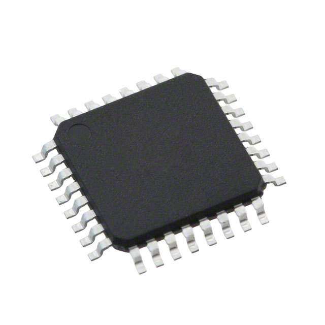
| 描述 | IC MCU 8BIT 7KB FLASH 44TQFP8位微控制器 -MCU 7KB FL 352R 36 I/O |
| EEPROM容量 | 256 x 8 |
| 产品分类 | |
| I/O数 | 35 |
| 品牌 | Microchip Technology |
| 产品手册 | |
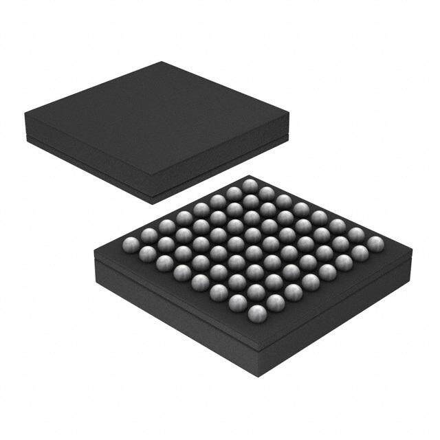
| 产品图片 |
|
| rohs | 符合RoHS无铅 / 符合限制有害物质指令(RoHS)规范要求 |
| 产品系列 | 嵌入式处理器和控制器,微控制器 - MCU,8位微控制器 -MCU,Microchip Technology PIC16F914-I/PTPIC® 16F |
| 数据手册 | http://www.microchip.com/mymicrochip/filehandler.aspx?ddocname=en020956http://www.microchip.com/mymicrochip/filehandler.aspx?ddocname=en023535http://www.microchip.com/mymicrochip/filehandler.aspx?ddocname=en531149http://www.microchip.com/mymicrochip/filehandler.aspx?ddocname=en541028http://www.microchip.com/mymicrochip/filehandler.aspx?ddocname=en020703 |
| 产品型号 | PIC16F914-I/PT |
| PCN组件/产地 | http://www.microchip.com/mymicrochip/NotificationDetails.aspx?id=5528&print=viewhttp://www.microchip.com/mymicrochip/NotificationDetails.aspx?id=5968&print=viewhttp://www.microchip.com/mymicrochip/NotificationDetails.aspx?pcn=IIRA-22KPRZ871&print=view |
| PCN设计/规格 | http://www.microchip.com/mymicrochip/NotificationDetails.aspx?id=5698&print=view |
| RAM容量 | 256 x 8 |
| 产品培训模块 | http://www.digikey.cn/PTM/IndividualPTM.page?site=cn&lang=zhs&ptm=2046http://www.digikey.cn/PTM/IndividualPTM.page?site=cn&lang=zhs&ptm=25053 |
| 产品目录页面 | |
| 产品种类 | 8位微控制器 -MCU |
| 供应商器件封装 | 44-TQFP(10x10) |
| 其它名称 | PIC16F914IPT |
| 包装 | 托盘 |
| 可用A/D通道 | 8 |
| 可编程输入/输出端数量 | 36 |
| 商标 | Microchip Technology |
| 处理器系列 | PIC16 |
| 外设 | 欠压检测/复位,LCD,POR,PWM,WDT |
| 安装风格 | SMD/SMT |
| 定时器数量 | 8 Timer |
| 封装 | Tray |
| 封装/外壳 | 44-TQFP |
| 封装/箱体 | TQFP-44 |
| 工作温度 | -40°C ~ 85°C |
| 工作电源电压 | 2 V to 5.5 V |
| 工厂包装数量 | 160 |
| 振荡器类型 | 内部 |
| 接口类型 | AUSART, I2C, SPI, SSP |
| 数据RAM大小 | 352 B |
| 数据Ram类型 | RAM |
| 数据ROM大小 | 256 B |
| 数据Rom类型 | EEPROM |
| 数据总线宽度 | 8 bit |
| 数据转换器 | A/D 8x10b |
| 最大工作温度 | + 85 C |
| 最大时钟频率 | 20 MHz |
| 最小工作温度 | - 40 C |
| 标准包装 | 160 |
| 核心 | PIC |
| 核心处理器 | PIC |
| 核心尺寸 | 8-位 |
| 片上ADC | Yes |
| 电压-电源(Vcc/Vdd) | 2 V ~ 5.5 V |
| 电源电压-最大 | 5.5 V |
| 电源电压-最小 | 4.5 V |
| 程序存储器大小 | 7 kB |
| 程序存储器类型 | Flash |
| 程序存储容量 | 7KB(4K x 14) |
| 系列 | PIC16 |
| 输入/输出端数量 | 36 I/O |
| 连接性 | I²C, SPI, UART/USART |
| 速度 | 20MHz |
| 配用 | /product-detail/zh/AC164305/AC164305-ND/613139/product-detail/zh/LABX1A/444-1001-ND/500789/product-detail/zh/AC164020/AC164020-ND/273319 |


- 商务部:美国ITC正式对集成电路等产品启动337调查
- 曝三星4nm工艺存在良率问题 高通将骁龙8 Gen1或转产台积电
- 太阳诱电将投资9.5亿元在常州建新厂生产MLCC 预计2023年完工
- 英特尔发布欧洲新工厂建设计划 深化IDM 2.0 战略
- 台积电先进制程称霸业界 有大客户加持明年业绩稳了
- 达到5530亿美元!SIA预计今年全球半导体销售额将创下新高
- 英特尔拟将自动驾驶子公司Mobileye上市 估值或超500亿美元
- 三星加码芯片和SET,合并消费电子和移动部门,撤换高东真等 CEO
- 三星电子宣布重大人事变动 还合并消费电子和移动部门
- 海关总署:前11个月进口集成电路产品价值2.52万亿元 增长14.8%


PDF Datasheet 数据手册内容提取
PIC16F913/914/916/917/946 Data Sheet 28/40/44/64-Pin Flash-Based, 8-Bit CMOS Microcontrollers with LCD Driver and nanoWatt Technology © 2007 Microchip Technology Inc. DS41250F
Note the following details of the code protection feature on Microchip devices: • Microchip products meet the specification contained in their particular Microchip Data Sheet. • Microchip believes that its family of products is one of the most secure families of its kind on the market today, when used in the intended manner and under normal conditions. • There are dishonest and possibly illegal methods used to breach the code protection feature. All of these methods, to our knowledge, require using the Microchip products in a manner outside the operating specifications contained in Microchip’s Data Sheets. Most likely, the person doing so is engaged in theft of intellectual property. • Microchip is willing to work with the customer who is concerned about the integrity of their code. • Neither Microchip nor any other semiconductor manufacturer can guarantee the security of their code. Code protection does not mean that we are guaranteeing the product as “unbreakable.” Code protection is constantly evolving. We at Microchip are committed to continuously improving the code protection features of our products. Attempts to break Microchip’s code protection feature may be a violation of the Digital Millennium Copyright Act. If such acts allow unauthorized access to your software or other copyrighted work, you may have a right to sue for relief under that Act. Information contained in this publication regarding device Trademarks applications and the like is provided only for your convenience The Microchip name and logo, the Microchip logo, Accuron, and may be superseded by updates. It is your responsibility to dsPIC, KEELOQ, KEELOQ logo, microID, MPLAB, PIC, ensure that your application meets with your specifications. PICmicro, PICSTART, PROMATE, PowerSmart, rfPIC, and MICROCHIP MAKES NO REPRESENTATIONS OR SmartShunt are registered trademarks of Microchip WARRANTIES OF ANY KIND WHETHER EXPRESS OR Technology Incorporated in the U.S.A. and other countries. IMPLIED, WRITTEN OR ORAL, STATUTORY OR OTHERWISE, RELATED TO THE INFORMATION, AmpLab, FilterLab, Linear Active Thermistor, Migratable INCLUDING BUT NOT LIMITED TO ITS CONDITION, Memory, MXDEV, MXLAB, PS logo, SEEVAL, SmartSensor QUALITY, PERFORMANCE, MERCHANTABILITY OR and The Embedded Control Solutions Company are FITNESS FOR PURPOSE. Microchip disclaims all liability registered trademarks of Microchip Technology Incorporated arising from this information and its use. Use of Microchip in the U.S.A. devices in life support and/or safety applications is entirely at Analog-for-the-Digital Age, Application Maestro, CodeGuard, the buyer’s risk, and the buyer agrees to defend, indemnify and dsPICDEM, dsPICDEM.net, dsPICworks, ECAN, hold harmless Microchip from any and all damages, claims, ECONOMONITOR, FanSense, FlexROM, fuzzyLAB, suits, or expenses resulting from such use. No licenses are In-Circuit Serial Programming, ICSP, ICEPIC, Mindi, MiWi, conveyed, implicitly or otherwise, under any Microchip MPASM, MPLAB Certified logo, MPLIB, MPLINK, PICkit, intellectual property rights. PICDEM, PICDEM.net, PICLAB, PICtail, PowerCal, PowerInfo, PowerMate, PowerTool, REAL ICE, rfLAB, rfPICDEM, Select Mode, Smart Serial, SmartTel, Total Endurance, UNI/O, WiperLock and ZENA are trademarks of Microchip Technology Incorporated in the U.S.A. and other countries. SQTP is a service mark of Microchip Technology Incorporated in the U.S.A. All other trademarks mentioned herein are property of their respective companies. © 2007, Microchip Technology Incorporated, Printed in the U.S.A., All Rights Reserved. Printed on recycled paper. Microchip received ISO/TS-16949:2002 certification for its worldwide headquarters, design and wafer fabrication facilities in Chandler and Tempe, Arizona; Gresham, Oregon and design centers in California and India. The Company’s quality system processes and procedures are for its PIC® MCUs and dsPIC® DSCs, KEELOQ® code hopping devices, Serial EEPROMs, microperipherals, nonvolatile memory and analog products. In addition, Microchip’s quality system for the design and manufacture of development systems is ISO 9001:2000 certified. DS41250F-page ii © 2007 Microchip Technology Inc.
PIC16F913/914/916/917/946 28/40/44/64-Pin Flash-Based, 8-Bit CMOS Microcontrollers with LCD Driver and nanoWatt Technology High-Performance RISC CPU: Low-Power Features: • Only 35 instructions to learn: • Standby Current: - All single-cycle instructions except branches - <100nA @ 2.0V, typical • Operating speed: • Operating Current: - DC – 20MHz oscillator/clock input - 11μA @ 32kHz, 2.0V, typical - DC – 200ns instruction cycle - 220μA @ 4MHz, 2.0V, typical • Program Memory Read (PMR) capability • Watchdog Timer Current: - 1μA @ 2.0V, typical • Interrupt capability • 8-level deep hardware stack Peripheral Features: • Direct, Indirect and Relative Addressing modes • Liquid Crystal Display module: Special Microcontroller Features: - Up to 60/96/168 pixel drive capability on 28/40/64-pin devices, respectively • Precision Internal Oscillator: - Four commons - Factory calibrated to ±1%, typical - Software selectable frequency range of • Up to 24/35/53 I/O pins and 1 input-only pin: 8MHz to 125kHz - High-current source/sink for direct LED drive - Software tunable - Interrupt-on-change pin - Two-Speed Start-up mode - Individually programmable weak pull-ups - External Oscillator fail detect for critical • In-Circuit Serial Programming™ (ICSP™) via two applications pins - Clock mode switching during operation for • Analog comparator module with: power savings - Two analog comparators • Software selectable 31kHz internal oscillator - Programmable on-chip voltage reference • Power-Saving Sleep mode (CVREF) module (% of VDD) • Wide operating voltage range (2.0V-5.5V) - Comparator inputs and outputs externally accessible • Industrial and Extended temperature range • A/D Converter: • Power-on Reset (POR) - 10-bit resolution and up to 8 channels • Power-up Timer (PWRT) and Oscillator Start-up • Timer0: 8-bit timer/counter with 8-bit Timer (OST) programmable prescaler • Brown-out Reset (BOR) with software control • Enhanced Timer1: option - 16-bit timer/counter with prescaler • Enhanced Low-Current Watchdog Timer (WDT) - External Timer1 Gate (count enable) with on-chip oscillator (software selectable - Option to use OSC1 and OSC2 as Timer1 nominal 268 seconds with full prescaler) with oscillator if INTOSCIO or LP mode is software enable selected • Multiplexed Master Clear with pull-up/input pin • Timer2: 8-bit timer/counter with 8-bit period • Programmable code protection register, prescaler and postscaler • High-Endurance Flash/EEPROM cell: • Addressable Universal Synchronous - 100,000 write Flash endurance Asynchronous Receiver Transmitter (AUSART) - 1,000,000 write EEPROM endurance • Up to 2 Capture, Compare, PWM modules: - Flash/Data EEPROM retention: > 40 years - 16-bit Capture, max. resolution 12.5ns - 16-bit Compare, max. resolution 200ns - 10-bit PWM, max. frequency 20kHz • Synchronous Serial Port (SSP) with I2C™ © 2007 Microchip Technology Inc. DS41250F-page 1
PIC16F913/914/916/917/946 Program Data Memory Memory LCD 10-bit A/D Timers Device I/O (segment CCP (ch) 8/16-bit Flash SRAM EEPROM drivers) (words/bytes) (bytes) (bytes) PIC16F913 4K/7K 256 256 24 5 16(1) 1 2/1 PIC16F914 4K/7K 256 256 35 8 24 2 2/1 PIC16F916 8K/14K 352 256 24 5 16(1) 1 2/1 PIC16F917 8K/14K 352 256 35 8 24 2 2/1 PIC16F946 8K/14K 336 256 53 8 42 2 2/1 Note 1: COM3 and SEG15 share the same physical pin on the PIC16F913/916, therefore SEG15 is not available when using 1/4 multiplex displays. Pin Diagrams – PIC16F914/917, 40-Pin 40-pin PDIP RE3/MCLR/VPP 1 40 RB7/ICSPDAT/ICDDAT/SEG13 RA0/AN0/C1-/SEG12 2 39 RB6/ICSPCLK/ICDCK/SEG14 RA1/AN1/C2-/SEG7 3 38 RB5/COM1 RA2/AN2/C2+/VREF-/COM2 4 37 RB4/COM0 RA3/AN3/C1+/VREF+/SEG15 5 36 RB3/SEG3 RA4/C1OUT/T0CKI/SEG4 6 35 RB2/SEG2 RA5/AN4/C2OUT/SS/SEG5 7 34 RB1/SEG1 RE0/AN5/SEG21 8 33 RB0/INT/SEG0 7 RE1/AN6/SEG22 9 1 32 VDD 9 RE2/AN7/SEG23 10 4/ 31 VSS 1 VDD 11 F9 30 RD7/SEG20 6 VSS 12 1 29 RD6/SEG19 C RA7/OSC1/CLKIN/T1OSI 13 PI 28 RD5/SEG18 RA6/OSC2/CLKOUT/T1OSO 14 27 RD4/SEG17 RC0/VLCD1 15 26 RC7/RX/DT/SDI/SDA/SEG8 RC1/VLCD2 16 25 RC6/TX/CK/SCK/SCL/SEG9 RC2/VLCD3 17 24 RC5/T1CKI/CCP1/SEG10 RC3/SEG6 18 23 RC4/T1G/SDO/SEG11 RD0/COM3 19 22 RD3/SEG16 RD1 20 21 RD2/CCP2 DS41250F-page 2 © 2007 Microchip Technology Inc.
PIC16F913/914/916/917/946 TABLE 1: PIC16F914/917 40-PIN SUMMARY I/O Pin A/D LCD Comparators Timers CCP AUSART SSP Interrupt Pull-Up Basic RA0 2 AN0 SEG12 C1- — — — — — — — RA1 3 AN1 SEG7 C2- — — — — — — — RA2 4 AN2/VREF- COM2 C2+ — — — — — — — RA3 5 AN3/VREF+ SEG15 C1+ — — — — — — — RA4 6 SEG4 C1OUT T0CKI — — — — — — RA5 7 AN4 SEG5 C2OUT — — — SS — — — RA6 14 — — — T1OSO — — — — — OSC2/CLKOUT RA7 13 — — — T1OSI — — — — — OSC1/CLKIN RB0 33 — SEG0 — — — — — INT Y — RB1 34 — SEG1 — — — — — — Y — RB2 35 — SEG2 — — — — — — Y — RB3 36 — SEG3 — — — — — — Y — RB4 37 — COM0 — — — — — IOC Y — RB5 38 — COM1 — — — — — IOC Y — RB6 39 — SEG14 — — — — — IOC Y ICSPCLK/ICDCK RB7 40 — SEG13 — — — — — IOC Y ICSPDAT/ICDDAT RC0 15 — VLCD1 — — — — — — — — RC1 16 — VLCD2 — — — — — — — — RC2 17 — VLCD3 — — — — — — — — RC3 18 — SEG6 — — — — — — — — RC4 23 — SEG11 — T1G — — SDO — — — RC5 24 — SEG10 — T1CKI CCP1 — — — — — RC6 25 — SEG9 — — — TX/CK SCK/SCL — — — RC7 26 — SEG8 — — — RX/DT SDI/SDA — — — RD0 19 — COM3 — — — — — — — — RD1 20 — — — — — — — — — — RD2 21 — — — — CCP2 — — — — — RD3 22 — SEG16 — — — — — — — — RD4 27 — SEG17 — — — — — — — — RD5 28 — SEG18 — — — — — — — — RD6 29 — SEG19 — — — — — — — — RD7 30 — SEG20 — — — — — — — — RE0 8 AN5 SEG21 — — — — — — — — RE1 9 AN6 SEG22 — — — — — — — — RE2 10 AN7 SEG23 — — — — — — — — RE3 1 — — — — — — — — Y(1) MCLR/VPP — 11 — — — — — — — — — VDD — 32 — — — — — — — — — VDD — 12 — — — — — — — — — VSS — 31 — — — — — — — — — VSS Note 1: Pull-up enabled only with external MCLR configuration. © 2007 Microchip Technology Inc. DS41250F-page 3
PIC16F913/914/916/917/946 Pin Diagrams – PIC16F913/916, 28-Pin 28-pin PDIP, SOIC, SSOP RE3/MCLR/VPP 1 28 RB7/ICSPDAT/ICDDAT/SEG13 RA0/AN0/C1-/SEG12 2 27 RB6/ICSPCLK/ICDCK/SEG14 RA1/AN1/C2-/SEG7 3 26 RB5/COM1 RA2/AN2/C2+/VREF-/COM2 4 25 RB4/COM0 RA3/AN3/C1+/VREF+/COM3/SEG15 5 24 RB3/SEG3 RA4/C1OUT/T0CKI/SEG4 6 6 23 RB2/SEG2 1 RA5/AN4/C2OUT/SS/SEG5 7 3/9 22 RB1/SEG1 VSS 8 91 21 RB0/INT/SEG0 RA7/OSC1/CLKIN/T1OSI 9 6F 20 VDD 1 RA6/OSC2/CLKOUT/T1OSO 10 C 19 VSS RC0/VLCD1 11 PI 18 RC7/RX/DT/SDI/SDA/SEG8 RC1/VLCD2 12 17 RC6/TX/CK/SCK/SCL/SEG9 RC2/VLCD3 13 16 RC5/T1CKI/CCP1/SEG10 RC3/SEG6 14 15 RC4/T1G/SDO/SEG11 28-pin QFN 3 1 4 G 1 E G S E 7 12 DAT/ CK/S G G D D E E C C 2-/S 1-/S VPP AT/I LK/I C C /R D C 1 0 N1/ N0/ CL SP SP OM OM A A M C C C C 1/ 0/ 3/ 7/I 6/I 5/ 4/ A A E B B B B R R R R R R R 8 7 6 5 4 3 2 2 2 2 2 2 2 2 RA2/AN2/C2+/VREF-/COM2 1 21 RB3/SEG3 RA3/AN3/C1+/VREF+/COM3/SEG15 2 20 RB2/SEG2 RA4/C1OUT/T0CKI/SEG4 3 19 RB1/SEG1 RA5/AN4/C2OUT/SS/SEG5 4 PIC16F913/916 18 RB0/INT/SEG0 VSS 5 17 VDD RA7/OSC1/CLKIN/T1OSI 6 16 VSS RA6/OSC2/CLKOUT/T1OSO 7 15 RC7/RX/DT/SDI/SDA/SEG8 0 1 2 3 4 8 9 1 1 1 1 1 1 2 3 6 1 0 9 D D D G 1 1 G C C C E G G E L L L S E E S 0/V 1/V 2/V C3/ O/S 1/S CL/ C C C R D P S R R R /S1G KI/CC SCK/ 4/T 1C CK/ RC RC5/T 6/TX/ C R DS41250F-page 4 © 2007 Microchip Technology Inc.
PIC16F913/914/916/917/946 TABLE 2: PIC16F913/916 28-PIN (PDIP, SOIC, SSOP) SUMMARY I/O Pin A/D LCD Comparators Timers CCP AUSART SSP Interrupt Pull-Up Basic RA0 2 AN0 SEG12 C1- — — — — — — — RA1 3 AN1 SEG7 C2- — — — — — — — RA2 4 AN2/VREF- COM2 C2+ — — — — — — — RA3 5 AN3/VREF+ SEG15/ C1+ — — — — — — — COM3 RA4 6 — SEG4 C1OUT T0CKI — — — — — — RA5 7 — SEG5 C2OUT — — — SS — — — RA6 10 — — — T1OSO — — — — — OSC2/CLKOUT RA7 9 — — — T1OSI — — — — — OSC1/CLKIN RB0 21 — SEG0 — — — — — INT Y — RB1 22 — SEG1 — — — — — — Y — RB2 23 — SEG2 — — — — — — Y — RB3 24 — SEG3 — — — — — — Y — RB4 25 — COM0 — — — — — IOC Y — RB5 26 — COM1 — — — — — IOC Y — RB6 27 — SEG14 — — — — — IOC Y ICSPCLK/ICDCK RB7 28 — SEG13 — — — — — IOC Y ICSPDAT/ICDDAT RC0 11 — VLCD1 — — — — — — — — RC1 12 — VLCD2 — — — — — — — — RC2 13 — VLCD3 — — — — — — — — RC3 14 — SEG6 — — — — — — — — RC4 15 — SEG11 — T1G — — SDO — — — RC5 16 — SEG10 — T1CKI CCP1 — — — — — RC6 17 — SEG9 — — — TX/CK SCK/SCL — — — RC7 18 — SEG8 — — — RX/DT SDI/SDA — — — RE3 1 — — — — — — — — Y(1) MCLR/VPP — 20 — — — — — — — — — VDD — 8 — — — — — — — — — VSS — 19 — — — — — — — — — VSS Note 1: Pull-up enabled only with external MCLR configuration. © 2007 Microchip Technology Inc. DS41250F-page 5
PIC16F913/914/916/917/946 TABLE 3: PIC16F913/916 28-PIN (QFN) SUMMARY I/O Pin A/D LCD Comparators Timers CCP AUSART SSP Interrupt Pull-Up Basic RA0 27 AN0 SEG12 C1- — — — — — — — RA1 28 AN1 SEG7 C2- — — — — — — — RA2 1 AN2/VREF- COM2 C2+ — — — — — — — RA3 2 AN3/VREF+ SEG15/ C1+ — — — — — — — COM3 RA4 3 — SEG4 C1OUT T0CKI — — — — — — RA5 4 AN4 SEG5 C2OUT — — — SS — — — RA6 7 — — — T1OSO — — — — — OSC2/CLKOUT RA7 6 — — — T1OSI — — — — — OSC1/CLKIN RB0 18 — SEG0 — — — — — INT Y — RB1 19 — SEG1 — — — — — — Y — RB2 20 — SEG2 — — — — — — Y — RB3 21 — SEG3 — — — — — — Y — RB4 22 — COM0 — — — — — IOC Y — RB5 23 — COM1 — — — — — IOC Y — RB6 24 — SEG14 — — — — — IOC Y ICSPCLK/ICDCK RB7 25 — SEG13 — — — — — IOC Y ICSPDAT/ICDDAT RC0 8 — VLCD1 — — — — — — — — RC1 9 — VLCD2 — — — — — — — — RC2 10 — VLCD3 — — — — — — — — RC3 11 — SEG6 — — — — — — — — RC4 12 — SEG11 — T1G — — SDO — — — RC5 13 — SEG10 — T1CKI CCP1 — — — — — RC6 14 — SEG9 — — — TX/CK SCK/SCL — — — RC7 15 — SEG8 — — — RX/DT SDI/SDA — — — RE3 26 — — — — — — — — Y(1) MCLR/VPP — 17 — — — — — — — — — VDD — 5 — — — — — — — — — VSS — 16 — — — — — — — — — VSS Note 1: Pull-up enabled only with external MCLR configuration. DS41250F-page 6 © 2007 Microchip Technology Inc.
PIC16F913/914/916/917/946 Pin Diagrams – PIC16F914/917, 44-Pin 9 G 44-pin TQFP CL/SESEG10G11 K/SP1/SE CCO/ X/CK/S1CKI/C1G/SDEG16CP2 OM3EG6LCD3LCD2 TTTSC CSVV 6/5/4/3/2/10/3/2/1/ CCCDDDDCCCC RRRRRRRRRRN 43210987654 RC7/RX/DT/SDI/SDA/SEG8 14444433333333 NC RD4/SEG17 2 32 RC0/VLCD1 RD5/SEG18 3 31 RA6/OSC2/CLKOUT/T1OSO RD6/SEG19 4 30 RA7/OSC1/CLKIN/T1OSI RD7/SEG20 5 29 VSS VSS 6 PIC16F914/917 28 VDD VDD 7 27 RE2/AN7/SEG23 RB0/SEG0/INT 8 26 RE1/AN6/SEG22 RB1/SEG1 9 25 RE0/AN5/SEG21 RB2/SEG2 10 24 RA5/AN4/C2OUT/SS/SEG5 RB3/SEG3 11 23 RA4/C1OUT/T0CKI/SEG4 23456789012 11111111222 CC0143P2725 NNRB4/COMRB5/COMRB6/ICSPCLK/ICDCK/SEG1RB7/ICSPDAT/ICDDAT/SEG1RE3/MCLR/VPRA0/C1-/AN0/SEG1RA1/C2-/AN1/SEGRA2/AN2/C2+/V-/COMREFRA3/AN3/V+/C1+/SEG1REF X/CK/SCK/SCL/SEG91CKI/CCP1/SEG101G/SDO/SEG11EG16CP2 OM3EG6LCD3LCD2LDC1 TTTSC CSVVV 6/5/4/3/2/10/3/2/1/0/ CCCDDDDCCCC RRRRRRRRRRR 44-pin QFN 43210987654 RC7/RX/DT/SDI/SDA/SEG8 14444433333333 RA6/OSC2/CLKOUT/T1OSO RD4/SEG17 2 32 RA7/OSC1/CLKIN/T1OSI RD5/SEG18 3 31 VSS RD6/SEG19 4 30 VSS RD7/SEG20 5 29 NC VSS 6 PIC16F914/917 28 VDD VDD 7 27 RE2/AN7/SEG23 VDD 8 26 RE1/AN6/SEG22 RB0/INT/SEG0 9 25 RE0/AN5/SEG21 RB1/SEG1 10 24 RA5/AN4/C2OUT/SS/SEG5 RB2/SEG2 11 23 RA4/C1OUT/T0CKI/SEG4 23456789012 11111111222 3C0143P2725 RB3/SEGNRB4/COMRB5/COMPCLK/ICDCK/SEG1DAT/ICDDAT/SEG1RE3/MCLR/VPRA0/AN0/C1-/SEG1RA1/AN1/C2-/SEGN2/C2+/V-/COMREF3/C1+/V+/SEG1REF SP AN RB6/ICB7/ICS RA2/RA3/A R © 2007 Microchip Technology Inc. DS41250F-page 7
PIC16F913/914/916/917/946 TABLE 4: PIC16F914/917 44-PIN (TQFP) SUMMARY I/O Pin A/D LCD Comparators Timers CCP AUSART SSP Interrupt Pull-Up Basic RA0 19 AN0 SEG12 C1- — — — — — — — RA1 20 AN1 SEG7 C2- — — — — — — — RA2 21 AN2/VREF- COM2 C2+ — — — — — — — RA3 22 AN3/VREF+ SEG15 C1+ — — — — — — — RA4 23 — SEG4 C1OUT T0CKI — — — — — — RA5 24 AN4 SEG5 C2OUT — — — SS — — — RA6 31 — — — T1OSO — — — — — OSC2/CLKOUT RA7 30 — — — T1OSI — — — — — OSC1/CLKIN RB0 8 — SEG0 — — — — — INT Y — RB1 9 — SEG1 — — — — — — Y — RB2 10 — SEG2 — — — — — — Y — RB3 11 — SEG3 — — — — — — Y — RB4 14 — COM0 — — — — — IOC Y — RB5 15 — COM1 — — — — — IOC Y — RB6 16 — SEG14 — — — — — IOC Y ICSPCLK/ICDCK RB7 17 — SEG13 — — — — — IOC Y ICSPDAT/ICDDAT RC0 32 — VLCD1 — — — — — — — — RC1 35 — VLCD2 — — — — — — — — RC2 36 — VLCD3 — — — — — — — — RC3 37 — SEG6 — — — — — — — — RC4 42 — SEG11 — T1G — — SDO — — — RC5 43 — SEG10 — T1CKI CCP1 — — — — — RC6 44 — SEG9 — — — TX/CK SCK/SCL — — — RC7 1 — SEG8 — — — RX/DT SDI/SDA — — — RD0 38 — COM3 — — — — — — — — RD1 39 — — — — — — — — — — RD2 40 — — — — CCP2 — — — — — RD3 41 — SEG16 — — — — — — — — RD4 2 — SEG17 — — — — — — — — RD5 3 — SEG18 — — — — — — — — RD6 4 — SEG19 — — — — — — — — RD7 5 — SEG20 — — — — — — — — RE0 25 AN5 SEG21 — — — — — — — — RE1 26 AN6 SEG22 — — — — — — — — RE2 27 AN7 SEG23 — — — — — — — — RE3 18 — — — — — — — — Y(1) MCLR/VPP — 7 — — — — — — — — — VDD — 28 — — — — — — — — — VDD — 6 — — — — — — — — — VSS — 29 — — — — — — — — — VSS — 12 — — — — — — — — — NC — 13 — — — — — — — — — NC — 33 — — — — — — — — — NC — 34 — — — — — — — — — NC Note 1: Pull-up enabled only with external MCLR configuration. DS41250F-page 8 © 2007 Microchip Technology Inc.
PIC16F913/914/916/917/946 TABLE 5: PIC16F914/917 44-PIN (QFN) SUMMARY I/O Pin A/D LCD Comparators Timers CCP AUSART SSP Interrupt Pull-Up Basic RA0 19 AN0 SEG12 C1- — — — — — — — RA1 20 AN1 SEG7 C2- — — — — — — — RA2 21 AN2/VREF- COM2 C2+ — — — — — — — RA3 22 AN3/VREF+ SEG15 C1+ — — — — — — — RA4 23 — SEG4 C1OUT T0CKI — — — — — — RA5 24 AN4 SEG5 C2OUT — — — SS — — — RA6 33 — — — T1OSO — — — — — OSC2/CLKOUT RA7 32 — — — T1OSI — — — — — OSC1/CLKIN RB0 9 — SEG0 — — — — — INT Y — RB1 10 — SEG1 — — — — — — Y — RB2 11 — SEG2 — — — — — — Y — RB3 12 — SEG3 — — — — — — Y — RB4 14 — COM0 — — — — — IOC Y — RB5 15 — COM1 — — — — — IOC Y — RB6 16 — SEG14 — — — — — IOC Y ICSPCLK/ICDCK RB7 17 — SEG13 — — — — — IOC Y ICSPDAT/ICDDAT RC0 34 — VLCD1 — — — — — — — — RC1 35 — VLCD2 — — — — — — — — RC2 36 — VLCD3 — — — — — — — — RC3 37 — SEG6 — — — — — — — — RC4 42 — SEG11 — T1G — — SDO — — — RC5 43 — SEG10 — T1CKI CCP1 — — — — — RC6 44 — SEG9 — — — TX/CK SCK/SCL — — — RC7 1 — SEG8 — — — RX/DT SDI/SDA — — — RD0 38 — COM3 — — — — — — — — RD1 39 — — — — — — — — — — RD2 40 — — — — CCP2 — — — — — RD3 41 — SEG16 — — — — — — — — RD4 2 — SEG17 — — — — — — — — RD5 3 — SEG18 — — — — — — — — RD6 4 — SEG19 — — — — — — — — RD7 5 — SEG20 — — — — — — — — RE0 25 AN5 SEG21 — — — — — — — — RE1 26 AN6 SEG22 — — — — — — — — RE2 27 AN7 SEG23 — — — — — — — — RE3 18 — — — — — — — — Y(1) MCLR/VPP — 7 — — — — — — — — — VDD — 8 — — — — — — — — — VDD — 28 — — — — — — — — — VDD — 6 — — — — — — — — — VSS — 30 — — — — — — — — — VSS — 13 — — — — — — — — — NC — 29 — — — — — — — — — NC Note 1: Pull-up enabled only with external MCLR configuration. © 2007 Microchip Technology Inc. DS41250F-page 9
PIC16F913/914/916/917/946 Pin Diagram – PIC16F946 64-pin TQFP DI/SDA/SEG8 CK/SCL/SEG9 CP1/SEG10 O/SEG11 EG18 EG17 X/DT/S X/CK/S 1CKI/C 1G/SD EG16 CP2 OM3 EG6 LCD3 LCD2 LCD1 S S R T T T S C C S V V V D5/ D4/ C7/ C6/ C5/ C4/ D3/ DD SS D2/ D1 D0/ C3/ C2/ C1/ C0/ R R R R R R R V V R R R R R R R 64 63 6261 60 59 58575655 54 53 52 51 5049 RD6/SEG19 1 48 RF7/SEG31 RD7/SEG20 2 47 RF6/SEG30 RG0/SEG36 3 46 RF5/SEG29 RG1/SEG37 4 45 RF4/SEG28 RG2/SEG38 5 44 RE7/SEG27 RG3/SEG39 6 43 RE6/SEG26 RG4/SEG40 7 42 RE5/SEG25 RG5/SEG41 8 PIC16F946 41 VSS VSS 9 40 RA6/OSC2/CLKOUT/T1OSO VDD 10 39 RA7/OSC1/CLKIN/T1OSI RF0/SEG32 11 38 VDD RF1/SEG33 12 37 RE4/SEG24 RF2/SEG34 13 36 RE3/MCLR/VPP RF3/SEG35 14 35 RE2/AN7/SEG23 RB0/INT/SEG0 15 34 RE1/AN6/SEG22 RB1/SEG1 16 33 RE0/AN5/SEG21 1718 19 20 21 22 23 24 25 26 27 28 29 30 31 32 2 3 D S 0 1 4 3 S D 2 7 4 5 RB2/SEG RB3/SEGVD VS RB4/COM RB5/COM B6/ICSPCLK/ICDCK/SEG1 7/ICSPDAT/ICDDAT/SEG1 AVS AVD RA0/AN0/C1-/SEG1 RA1/AN1/C2-/SEG RA2/AN2/C2+/V-/COM2REFA3/AN3/C1+/V+/SEG15REF RA4/C1OUT/T0CKI/SEG RA5/AN4/C2OUT/SS/SEG R B R R DS41250F-page 10 © 2007 Microchip Technology Inc.
PIC16F913/914/916/917/946 TABLE 6: PIC16F946 64-PIN (TQFP) SUMMARY I/O Pin A/D LCD Comparators Timers CCP AUSART SSP Interrupt Pull-Up Basic RA0 27 AN0 SEG12 C1- — — — — — — — RA1 28 AN1 SEG7 C2- — — — — — — — RA2 29 AN2/VREF- COM2 C2+ — — — — — — — RA3 30 AN3/VREF+ SEG15 C1+ — — — — — — — RA4 31 — SEG4 C1OUT T0CKI — — — — — — RA5 32 AN4 — C2OUT — — — SS — — — RA6 40 SEG5 — — T1OSO — — — — — OSC2/CLKOUT RA7 39 — — — T1OSI — — — — — OSC1/CLKIN RB0 15 — SEG0 — — — — — INT Y — RB1 16 — SEG1 — — — — — — Y — RB2 17 — SEG2 — — — — — — Y — RB3 18 — SEG3 — — — — — — Y — RB4 21 — COM0 — — — — — IOC Y — RB5 22 — COM1 — — — — — IOC Y — RB6 23 — SEG14 — — — — — IOC Y ICSPCLK/ICDCK RB7 24 — SEG13 — — — — — IOC Y ICSPDAT/ICDDAT RC0 49 — VLCD1 — — — — — — — — RC1 50 — VLCD2 — — — — — — — — RC2 51 — VLCD3 — — — — — — — — RC3 52 — SEG6 — — — — — — — — RC4 59 — SEG11 — T1G — — SDO — — — RC5 60 — SEG10 — T1CKI CCP1 — — — — — RC6 61 — SEG9 — — — TX/CK SCK/SCL — — — RC7 62 — SEG8 — — — RX/DT SDI/SDA — — — RD0 53 — COM3 — — — — — — — — RD1 54 — — — — — — — — — — RD2 55 — — — — CCP2 — — — — — RD3 58 — SEG16 — — — — — — — — RD4 63 — SEG17 — — — — — — — — RD5 64 — SEG18 — — — — — — — — RD6 1 — SEG19 — — — — — — — — RD7 2 — SEG20 — — — — — — — — RE0 33 AN5 SEG21 — — — — — — — — RE1 34 AN6 SEG22 — — — — — — — — RE2 35 AN7 SEG23 — — — — — — — — RE3 36 — — — — — — — — Y(1) MCLR/VPP RE4 37 — SEG24 — — — — — — — — RE5 42 — SEG25 — — — — — — — — RE6 43 — SEG26 — — — — — — — — RE7 44 — SEG27 — — — — — — — — RF0 11 — SEG32 — — — — — — — — RF1 12 — SEG33 — — — — — — — — RF2 13 — SEG34 — — — — — — — — Note 1: Pull-up enabled only with external MCLR configuration. © 2007 Microchip Technology Inc. DS41250F-page 11
PIC16F913/914/916/917/946 TABLE 6: PIC16F946 64-PIN (TQFP) SUMMARY (CONTINUED) I/O Pin A/D LCD Comparators Timers CCP AUSART SSP Interrupt Pull-Up Basic RF3 14 — SEG35 — — — — — — — — RF4 45 — SEG28 — — — — — — — — RF5 46 — SEG29 — — — — — — — — RF6 47 — SEG30 — — — — — — — — RF7 48 — SEG31 — — — — — — — — RG0 3 — SEG36 — — — — — — — — RG1 4 — SEG37 — — — — — — — — RG2 5 — SEG38 — — — — — — — — RG3 6 — SEG39 — — — — — — — — RG4 7 — SEG40 — — — — — — — — RG5 8 — SEG41 — — — — — — — — — 26 — — — — — — — — — AVDD — 25 — — — — — — — — — AVSS — 10 — — — — — — — — — VDD — 19 — — — — — — — — — VDD — 38 — — — — — — — — — VDD — 57 — — — — — — — — — VDD — 9 — — — — — — — — — VSS — 20 — — — — — — — — — VSS — 41 — — — — — — — — — VSS — 56 — — — — — — — — — VSS Note 1: Pull-up enabled only with external MCLR configuration. DS41250F-page 12 © 2007 Microchip Technology Inc.
PIC16F913/914/916/917/946 Table of Contents 1.0 Device Overview........................................................................................................................................................................15 2.0 Memory Organization.................................................................................................................................................................23 3.0 I/O Ports.....................................................................................................................................................................................43 4.0 Oscillator Module (With Fail-Safe Clock Monitor).......................................................................................................................87 5.0 Timer0 Module...........................................................................................................................................................................99 6.0 Timer1 Module with Gate Control.............................................................................................................................................102 7.0 Timer2 Module.........................................................................................................................................................................107 8.0 Comparator Module..................................................................................................................................................................109 9.0 Addressable Universal Synchronous Asynchronous Receiver Transmitter (AUSART)...........................................................121 10.0 Liquid Crystal Display (LCD) Driver Module.............................................................................................................................143 11.0 Programmable Low-Voltage Detect (PLVD) Module................................................................................................................171 12.0 Analog-to-Digital Converter (ADC) Module..............................................................................................................................175 13.0 Data EEPROM and Flash Program Memory Control...............................................................................................................187 14.0 SSP Module Overview.............................................................................................................................................................193 15.0 Capture/Compare/PWM (CCP) Module...................................................................................................................................211 16.0 Special Features of the CPU....................................................................................................................................................219 17.0 Instruction Set Summary..........................................................................................................................................................241 18.0 Development Support...............................................................................................................................................................251 19.0 Electrical Specifications............................................................................................................................................................255 20.0 DC and AC Characteristics Graphs and Tables.......................................................................................................................283 21.0 Packaging Information..............................................................................................................................................................305 Appendix A: Data Sheet Revision History..........................................................................................................................................315 Appendix B: Migrating From Other PIC® Devices..............................................................................................................................315 Appendix C: Conversion Considerations...........................................................................................................................................316 Index..................................................................................................................................................................................................317 The Microchip Web Site.....................................................................................................................................................................325 Customer Change Notification Service..............................................................................................................................................325 Customer Support..............................................................................................................................................................................325 Reader Response..............................................................................................................................................................................327 Product Identification System............................................................................................................................................................328 TO OUR VALUED CUSTOMERS It is our intention to provide our valued customers with the best documentation possible to ensure successful use of your Microchip products. To this end, we will continue to improve our publications to better suit your needs. Our publications will be refined and enhanced as new volumes and updates are introduced. If you have any questions or comments regarding this publication, please contact the Marketing Communications Department via E-mail at docerrors@microchip.com or fax the Reader Response Form in the back of this data sheet to (480) 792-4150. We welcome your feedback. Most Current Data Sheet To obtain the most up-to-date version of this data sheet, please register at our Worldwide Web site at: http://www.microchip.com You can determine the version of a data sheet by examining its literature number found on the bottom outside corner of any page. The last character of the literature number is the version number, (e.g., DS30000A is version A of document DS30000). Errata An errata sheet, describing minor operational differences from the data sheet and recommended workarounds, may exist for current devices. As device/documentation issues become known to us, we will publish an errata sheet. The errata will specify the revision of silicon and revision of document to which it applies. To determine if an errata sheet exists for a particular device, please check with one of the following: • Microchip’s Worldwide Web site; http://www.microchip.com • Your local Microchip sales office (see last page) When contacting a sales office, please specify which device, revision of silicon and data sheet (include literature number) you are using. Customer Notification System Register on our web site at www.microchip.com to receive the most current information on all of our products. © 2007 Microchip Technology Inc. DS41250F-page 13
PIC16F913/914/916/917/946 NOTES: DS41250F-page 14 © 2007 Microchip Technology Inc.
PIC16F913/914/916/917/946 1.0 DEVICE OVERVIEW The PIC16F91X/946 devices are covered by this data sheet. They are available in 28/40/44/64-pin packages. Figure1-1 shows a block diagram of the PIC16F913/916 device, Figure1-2 shows a block diagram of the PIC16F914/917 device, and Figure1-3 shows a block diagram of the PIC16F946 device. Table1-1 shows the pinout descriptions. FIGURE 1-1: PIC16F913/916 BLOCK DIAGRAM INT Configuration 13 8 Data Bus PORTA Program Counter RA0 Flash RA1 4K/8K x 14 RA2 Program 8-Level Stack (13-bit) RAM RA3 Memory 256/352 bytes RA4 File RA5 Registers RA7 Program 14 Bus Program Memory Read RAM Addr (PMR) 9 PORTB Addr MUX RB0 Instruction Reg RB1 Direct Addr 7 Indirect RB2 8 Addr RB3 RB4 FSR Reg RB5 RB6 STATUS Reg RB7 8 PORTC RC0 3 MUX RC1 Power-up RC2 Timer RC3 Instruction RC4 Decode and Oscillator Control Start-up Timer ALU RC5 RC6 OSC1/CLKIN Power-on 8 RC7 Reset Timing OSC2/CLKOUT Generation Watchdog W Reg PORTE Timer Brown-out Reset Internal RE3/MCLR Oscillator Block VDD VSS Data EEPROM 256 bytes Timer0 Timer1 Timer2 10-bit A/D Addressable Comparators CCP1 SSP PLVD LCD USART © 2007 Microchip Technology Inc. DS41250F-page 15
PIC16F913/914/916/917/946 FIGURE 1-2: PIC16F914/917 BLOCK DIAGRAM INT Configuration 13 8 Data Bus PORTA Program Counter RA0 Flash RA1 4K/8K x 14 RA2 Program RAM RA3 8-Level Stack (13-bit) RA4 Memory 256/352 bytes RA5 File RA6 Registers RA7 Program 14 Bus Program Memory Read RAM Addr (PMR) 9 PORTB Addr MUX RB0 Instruction Reg RB1 Direct Addr 7 Indirect RB2 8 Addr RB3 RB4 FSR Reg RB5 RB6 STATUS Reg RB7 8 PORTC RC0 3 MUX RC1 Power-up RC2 Timer RC3 Instruction RC4 Decode and Oscillator Control Start-up Timer ALU RC5 RC6 OSC1/CLKIN Power-on 8 RC7 Reset Timing OSC2/CLKOUT Generation Watchdog W Reg PORTD Timer RD0 RD1 Brown-out RD2 Reset RD3 Internal RD4 Oscillator Block RD5 RD6 VDD VSS RD7 PORTE RE0 RE1 RE2 RE3/MCLR Timer0 Timer1 Timer2 10-bit A/D Data EEPROM 256 bytes Addressable Comparators CCP1 CCP2 SSP PLVD LCD USART DS41250F-page 16 © 2007 Microchip Technology Inc.
PIC16F913/914/916/917/946 FIGURE 1-3: PIC16F946 BLOCK DIAGRAM INT PORTA Configuration RA0 13 Data Bus 8 RA1 Program Counter RA2 Flash RA3 RA4 8K x 14 RA5 Program 8-Level Stack (13-bit) RAM RA6 Memory 336 x 8 bytes RA7 File PORTB Registers RB0 Program 14 Bus Program Memory Read RAM Addr RB1 (PMR) 9 RB2 RB3 Addr MUX RB4 Instruction Reg Direct Addr 7 Indirect RB5 8 Addr RB6 RB7 FSR Reg PORTC RC0 8 STATUS Reg RC1 RC2 RC3 Power-up RC4 Timer 3 MUX RC5 RC6 Oscillator RC7 Instruction Start-up Timer PORTD Decode and Control Power-on ALU RD0 Reset RD1 OSC1/CLKIN Watchdog 8 RD2 Timing Timer RD3 OSC2/CLKOUT Generation Brown-out W Reg RD4 RD5 Reset RD6 RD7 Internal PORTE Oscillator Block VDD VSS RE0 RE1 RE2 RE3/MCLR RE4 RE5 RE6 RE7 PORTF RF0 RF1 RF2 RF3 RF4 RF5 RF6 RF7 PORTG RG0 RG1 RG2 RG3 AVDD AVSS RG4 RG5 Data EEPROM Timer0 Timer1 Timer2 10-bit A/D 256 bytes Addressable Comparators CCP1 CCP2 SSP PLVD LCD USART © 2007 Microchip Technology Inc. DS41250F-page 17
PIC16F913/914/916/917/946 TABLE 1-1: PIC16F91X/946 PINOUT DESCRIPTIONS Input Output Name Function Description Type Type RA0/AN0/C1-/SEG12 RA0 TTL CMOS General purpose I/O. AN0 AN — Analog input Channel 0. C1- AN — Comparator 1 negative input. SEG12 — AN LCD analog output. RA1/AN1/C2-/SEG7 RA1 TTL CMOS General purpose I/O. AN1 AN — Analog input Channel 1. C2- AN — Comparator 2 negative input. SEG7 — AN LCD analog output. RA2/AN2/C2+/VREF-/COM2 RA2 TTL CMOS General purpose I/O. AN2 AN — Analog input Channel 2. C2+ AN — Comparator 2 positive input. VREF- AN — External A/D Voltage Reference – negative. COM2 — AN LCD analog output. RA3/AN3/C1+/VREF+/COM3(1)/ RA3 TTL CMOS General purpose I/O. SEG15 AN3 AN — Analog input Channel 3. C1+ AN — Comparator 1 positive input. VREF+ AN — External A/D Voltage Reference – positive. COM3(1) — AN LCD analog output. SEG15 — AN LCD analog output. RA4/C1OUT/T0CKI/SEG4 RA4 TTL CMOS General purpose I/O. C1OUT — CMOS Comparator 1 output. T0CKI ST — Timer0 clock input. SEG4 — AN LCD analog output. RA5/AN4/C2OUT/SS/SEG5 RA5 TTL CMOS General purpose I/O. AN4 AN — Analog input Channel 4. C2OUT — CMOS Comparator 2 output. SS TTL — Slave select input. SEG5 — AN LCD analog output. RA6/OSC2/CLKOUT/T1OSO RA6 TTL CMOS General purpose I/O. OSC2 — XTAL Crystal/Resonator. CLKOUT — CMOS TOSC/4 reference clock. T1OSO — XTAL Timer1 oscillator output. RA7/OSC1/CLKIN/T1OSI RA7 TTL CMOS General purpose I/O. OSC1 XTAL — Crystal/Resonator. CLKIN ST — Clock input. T1OSI XTAL — Timer1 oscillator input. RB0/INT/SEG0 RB0 TTL CMOS General purpose I/O. Individually enabled pull-up. INT ST — External interrupt pin. SEG0 — AN LCD analog output. Legend: AN = Analog input or output CMOS= CMOS compatible input or output OD= Open Drain TTL = TTL compatible input ST = Schmitt Trigger input with CMOS levels P = Power HV = High Voltage XTAL = Crystal Note 1: COM3 is available on RA3 for the PIC16F913/916 and on RD0 for the PIC16F914/917 and PIC16F946. 2: Pins available on PIC16F914/917 and PIC16F946 only. 3: Pins available on PIC16F946 only. 4: I2C Schmitt trigger inputs have special input levels. DS41250F-page 18 © 2007 Microchip Technology Inc.
PIC16F913/914/916/917/946 TABLE 1-1: PIC16F91X/946 PINOUT DESCRIPTIONS (CONTINUED) Input Output Name Function Description Type Type RB1/SEG1 RB1 TTL CMOS General purpose I/O. Individually enabled pull-up. SEG1 — AN LCD analog output. RB2/SEG2 RB2 TTL CMOS General purpose I/O. Individually enabled pull-up. SEG2 — AN LCD analog output. RB3/SEG3 RB3 TTL CMOS General purpose I/O. Individually enabled pull-up. SEG3 — AN LCD analog output. RB4/COM0 RB4 TTL CMOS General purpose I/O. Individually controlled interrupt-on-change. Individually enabled pull-up. COM0 — AN LCD analog output. RB5/COM1 RB5 TTL CMOS General purpose I/O. Individually controlled interrupt-on-change. Individually enabled pull-up. COM1 — AN LCD analog output. RB6/ICSPCLK/ICDCK/SEG14 RB6 TTL CMOS General purpose I/O. Individually controlled interrupt-on-change. Individually enabled pull-up. ICSPCLK ST — ICSP™ clock. ICDCK ST — ICD clock. SEG14 — AN LCD analog output. RB7/ICSPDAT/ICDDAT/SEG13 RB7 TTL CMOS General purpose I/O. Individually controlled inter- rupt-on-change. Individually enabled pull-up. ICSPDAT ST CMOS ICSP Data I/O. ICDDAT ST CMOS ICD Data I/O. SEG13 — AN LCD analog output. RC0/VLCD1 RC0 ST CMOS General purpose I/O. VLCD1 AN — LCD analog input. RC1/VLCD2 RC1 ST CMOS General purpose I/O. VLCD2 AN — LCD analog input. RC2/VLCD3 RC2 ST CMOS General purpose I/O. VLCD3 AN — LCD analog input. RC3/SEG6 RC3 ST CMOS General purpose I/O. SEG6 — AN LCD analog output. RC4/T1G/SDO/SEG11 RC4 ST CMOS General purpose I/O. T1G ST — Timer1 gate input. SDO — CMOS Serial data output. SEG11 — AN LCD analog output. RC5/T1CKI/CCP1/SEG10 RC5 ST CMOS General purpose I/O. T1CKI ST — Timer1 clock input. CCP1 ST CMOS Capture 1 input/Compare 1 output/PWM 1 output. SEG10 — AN LCD analog output. Legend: AN = Analog input or output CMOS= CMOS compatible input or output OD= Open Drain TTL = TTL compatible input ST = Schmitt Trigger input with CMOS levels P = Power HV = High Voltage XTAL = Crystal Note 1: COM3 is available on RA3 for the PIC16F913/916 and on RD0 for the PIC16F914/917 and PIC16F946. 2: Pins available on PIC16F914/917 and PIC16F946 only. 3: Pins available on PIC16F946 only. 4: I2C Schmitt trigger inputs have special input levels. © 2007 Microchip Technology Inc. DS41250F-page 19
PIC16F913/914/916/917/946 TABLE 1-1: PIC16F91X/946 PINOUT DESCRIPTIONS (CONTINUED) Input Output Name Function Description Type Type RC6/TX/CK/SCK/SCL/SEG9 RC6 ST CMOS General purpose I/O. TX — CMOS USART asynchronous serial transmit. CK ST CMOS USART synchronous serial clock. SCK ST CMOS SPI clock. SCL ST(4) OD I2C™ clock. SEG9 — AN LCD analog output. RC7/RX/DT/SDI/SDA/SEG8 RC7 ST CMOS General purpose I/O. RX ST — USART asynchronous serial receive. DT ST CMOS USART synchronous serial data. SDI ST CMOS SPI data input. SDA ST(4) OD I2C™ data. SEG8 — AN LCD analog output. RD0/COM3(1, 2) RD0 ST CMOS General purpose I/O. COM3 — AN LCD analog output. RD1(2) RD1 ST CMOS General purpose I/O. RD2/CCP2(2) RD2 ST CMOS General purpose I/O. CCP2 ST CMOS Capture 2 input/Compare 2 output/PWM 2 output. RD3/SEG16(2) RD3 ST CMOS General purpose I/O. SEG16 — AN LCD analog output. RD4/SEG17(2) RD4 ST CMOS General purpose I/O. SEG17 — AN LCD analog output. RD5/SEG18(2) RD5 ST CMOS General purpose I/O. SEG18 — AN LCD analog output. RD6/SEG19(2) RD6 ST CMOS General purpose I/O. SEG19 — AN LCD analog output. RD7/SEG20(2) RD7 ST CMOS General purpose I/O. SEG20 — AN LCD analog output. RE0/AN5/SEG21(2) RE0 ST CMOS General purpose I/O. AN5 AN — Analog input Channel 5. SEG21 — AN LCD analog output. RE1/AN6/SEG22(2) RE1 ST CMOS General purpose I/O. AN6 AN — Analog input Channel 6. SEG22 — AN LCD analog output. RE2/AN7/SEG23(2) RE2 ST CMOS General purpose I/O. AN7 AN — Analog input Channel 7. SEG23 — AN LCD analog output. RE3/MCLR/VPP RE3 ST — Digital input only. MCLR ST — Master Clear with internal pull-up. VPP HV — Programming voltage. Legend: AN = Analog input or output CMOS= CMOS compatible input or output OD= Open Drain TTL = TTL compatible input ST = Schmitt Trigger input with CMOS levels P = Power HV = High Voltage XTAL = Crystal Note 1: COM3 is available on RA3 for the PIC16F913/916 and on RD0 for the PIC16F914/917 and PIC16F946. 2: Pins available on PIC16F914/917 and PIC16F946 only. 3: Pins available on PIC16F946 only. 4: I2C Schmitt trigger inputs have special input levels. DS41250F-page 20 © 2007 Microchip Technology Inc.
PIC16F913/914/916/917/946 TABLE 1-1: PIC16F91X/946 PINOUT DESCRIPTIONS (CONTINUED) Input Output Name Function Description Type Type RE4/SEG24(3) RE4 ST CMOS General purpose I/O. SEG24 — AN LCD analog output. RE5/SEG25(3) RE5 ST CMOS General purpose I/O. SEG25 — AN LCD analog output. RE6/SEG26(3) RE6 ST CMOS General purpose I/O. SEG26 — AN LCD analog output. RE7/SEG27(3) RE7 ST CMOS General purpose I/O. SEG27 — AN LCD analog output. RF0/SEG32(3) RF0 ST CMOS General purpose I/O. SEG32 — AN LCD analog output. RF1/SEG33(3) RF1 ST CMOS General purpose I/O. SEG33 — AN LCD analog output. RF2/SEG34(3) RF2 ST CMOS General purpose I/O. SEG34 — AN LCD analog output. RF3/SEG35(3) RF3 ST CMOS General purpose I/O. SEG35 — AN LCD analog output. RF4/SEG28(3) RF4 ST CMOS General purpose I/O. SEG28 — AN LCD analog output. RF5/SEG29(3) RF5 ST CMOS General purpose I/O. SEG29 — AN LCD analog output. RF6/SEG30(3) RF6 ST CMOS General purpose I/O. SEG30 — AN LCD analog output. RF7/SEG31(3) RF7 ST CMOS General purpose I/O. SEG31 — AN LCD analog output. RG0/SEG36(3) RG0 ST CMOS General purpose I/O. SEG36 — AN LCD analog output. RG1/SEG37(3) RG1 ST CMOS General purpose I/O. SEG37 — AN LCD analog output. RG2/SEG38(3) RG2 ST CMOS General purpose I/O. SEG38 — AN LCD analog output. RG3/SEG39(3) RG3 ST CMOS General purpose I/O. SEG39 — AN LCD analog output. RG4/SEG40(3) RG4 ST CMOS General purpose I/O. SEG10 — AN LCD analog output. RG5/SEG41(3) RG5 ST CMOS General purpose I/O. SEG41 — AN LCD analog output. AVDD(3) AVDD P — Analog power supply for microcontroller. AVSS(3) AVSS P — Analog ground reference for microcontroller. VDD VDD P — Power supply for microcontroller. Legend: AN = Analog input or output CMOS= CMOS compatible input or output OD= Open Drain TTL = TTL compatible input ST = Schmitt Trigger input with CMOS levels P = Power HV = High Voltage XTAL = Crystal Note 1: COM3 is available on RA3 for the PIC16F913/916 and on RD0 for the PIC16F914/917 and PIC16F946. 2: Pins available on PIC16F914/917 and PIC16F946 only. 3: Pins available on PIC16F946 only. 4: I2C Schmitt trigger inputs have special input levels. © 2007 Microchip Technology Inc. DS41250F-page 21
PIC16F913/914/916/917/946 TABLE 1-1: PIC16F91X/946 PINOUT DESCRIPTIONS (CONTINUED) Input Output Name Function Description Type Type VSS VSS P — Ground reference for microcontroller. Legend: AN = Analog input or output CMOS= CMOS compatible input or output OD= Open Drain TTL = TTL compatible input ST = Schmitt Trigger input with CMOS levels P = Power HV = High Voltage XTAL = Crystal Note 1: COM3 is available on RA3 for the PIC16F913/916 and on RD0 for the PIC16F914/917 and PIC16F946. 2: Pins available on PIC16F914/917 and PIC16F946 only. 3: Pins available on PIC16F946 only. 4: I2C Schmitt trigger inputs have special input levels. DS41250F-page 22 © 2007 Microchip Technology Inc.
PIC16F913/914/916/917/946 2.0 MEMORY ORGANIZATION FIGURE 2-2: PROGRAM MEMORY MAP AND STACK FOR THE 2.1 Program Memory Organization PIC16F916/917/PIC16F946 The PIC16F91X/946 has a 13-bit program counter pc<12:0> capable of addressing a 4K x14 program memory CALL, RETURN 13 space for the PIC16F913/914 (0000h-0FFFh) and an RETFIE, RETLW 8K x14 program memory space for the PIC16F916/ 917 and PIC16F946 (0000h-1FFFh). Accessing a Stack Level 1 location above the memory boundaries for the Stack Level 2 PIC16F913 and PIC16F914 will cause a wrap around within the first 4Kx14 space. The Reset vector is at 0000h and the interrupt vector is at 0004h. Stack Level 8 FIGURE 2-1: PROGRAM MEMORY MAP Reset Vector 0000h AND STACK FOR THE PIC16F913/914 Interrupt Vector 0004h 0005h pc<12:0> Page 0 CALL, RETURN 13 07FFh RETFIE, RETLW 0800h Page 1 On-chip Stack Level 1 0FFFh Program Stack Level 2 1000h Memory Page 2 17FFh Stack Level 8 1800h Page 3 Reset Vector 0000h 1FFFh Interrupt Vector 0004h 0005h Page 0 On-chip 07FFh Program 0800h Memory Page 1 0FFFh 1000h 1FFFh © 2007 Microchip Technology Inc. DS41250F-page 23
PIC16F913/914/916/917/946 2.2 Data Memory Organization The data memory is partitioned into multiple banks which contain the General Purpose Registers (GPRs) and the Special Function Registers (SFRs). Bits RP0 and RP1 are bank select bits. RP1 RP0 0 0 → Bank 0 is selected 0 1 → Bank 1 is selected 1 0 → Bank 2 is selected 1 1 → Bank 3 is selected Each bank extends up to 7Fh (128 bytes). The lower locations of each bank are reserved for the Special Function Registers. Above the Special Function Registers are the General Purpose Registers, implemented as static RAM. All implemented banks contain Special Function Registers. Some frequently used Special Function Registers from one bank are mirrored in another bank for code reduction and quicker access. 2.2.1 GENERAL PURPOSE REGISTER FILE The register file is organized as 256x8 bits in the PIC16F913/914, 352x8 bits in the PIC16F916/917 and 336x8 bits in the PIC16F946. Each register is accessed either directly or indirectly through the File Select Register (FSR) (see Section2.5 “Indirect Addressing, INDF and FSR Registers”). 2.2.2 SPECIAL FUNCTION REGISTERS The Special Function Registers are registers used by the CPU and peripheral functions for controlling the desired operation of the device (see Tables2-1, 2-2, 2-3 and 2-4). These registers are static RAM. The Special Function Registers can be classified into two sets: core and peripheral. The Special Function Registers associated with the “core” are described in this section. Those related to the operation of the peripheral features are described in the section of that peripheral feature. DS41250F-page 24 © 2007 Microchip Technology Inc.
PIC16F913/914/916/917/946 FIGURE 2-3: PIC16F913/916 SPECIAL FUNCTION REGISTERS File File File File Address Address Address Address Indirect addr. (1) 00h Indirect addr. (1) 80h Indirect addr. (1) 100h Indirect addr. (1) 180h TMR0 01h OPTION_REG 81h TMR0 101h OPTION_REG 181h PCL 02h PCL 82h PCL 102h PCL 182h STATUS 03h STATUS 83h STATUS 103h STATUS 183h FSR 04h FSR 84h FSR 104h FSR 184h PORTA 05h TRISA 85h WDTCON 105h 185h PORTB 06h TRISB 86h PORTB 106h TRISB 186h PORTC 07h TRISC 87h LCDCON 107h 187h 08h 88h LCDPS 108h 188h PORTE 09h TRISE 89h LVDCON 109h 189h PCLATH 0Ah PCLATH 8Ah PCLATH 10Ah PCLATH 18Ah INTCON 0Bh INTCON 8Bh INTCON 10Bh INTCON 18Bh PIR1 0Ch PIE1 8Ch EEDATL 10Ch EECON1 18Ch PIR2 0Dh PIE2 8Dh EEADRL 10Dh EECON2(1) 18Dh TMR1L 0Eh PCON 8Eh EEDATH 10Eh Reserved 18Eh TMR1H 0Fh OSCCON 8Fh EEADRH 10Fh Reserved 18Fh T1CON 10h OSCTUNE 90h LCDDATA0 110h 190h TMR2 11h ANSEL 91h LCDDATA1 111h T2CON 12h PR2 92h 112h SSPBUF 13h SSPADD 93h LCDDATA3 113h SSPCON 14h SSPSTAT 94h LCDDATA4 114h CCPR1L 15h WPUB 95h 115h CCPR1H 16h IOCB 96h LCDDATA6 116h CCP1CON 17h CMCON1 97h LCDDATA7 117h RCSTA 18h TXSTA 98h 118h TXREG 19h SPBRG 99h LCDDATA9 119h General RCREG 1Ah 9Ah LCDDATA10 11Ah Purpose 1Bh 9Bh 11Bh Register(2) 1Ch CMCON0 9Ch LCDSE0 11Ch 96 Bytes 1Dh VRCON 9Dh LCDSE1 11Dh ADRESH 1Eh ADRESL 9Eh 11Eh ADCON0 1Fh ADCON1 9Fh 11Fh 20h A0h 120h General General General Purpose Purpose Purpose Register Register Register 80 Bytes 80 Bytes 96 Bytes EFh 16Fh 1EFh accesses F0h accesses 170h accesses 1F0h 7Fh 70h-7Fh FFh 70h-7Fh 17Fh 70h-7Fh 1FFh Bank 0 Bank 1 Bank 2 Bank 3 Unimplemented data memory locations, read as ‘0’. Note 1: Not a physical register. 2: On the PIC16F913, unimplemented data memory locations, read as ‘0’. © 2007 Microchip Technology Inc. DS41250F-page 25
PIC16F913/914/916/917/946 FIGURE 2-4: PIC16F914/917 SPECIAL FUNCTION REGISTERS File File File File Address Address Address Address Indirect addr. (1) 00h Indirect addr. (1) 80h Indirect addr. (1) 100h Indirect addr. (1) 180h TMR0 01h OPTION_REG 81h TMR0 101h OPTION_REG 181h PCL 02h PCL 82h PCL 102h PCL 182h STATUS 03h STATUS 83h STATUS 103h STATUS 183h FSR 04h FSR 84h FSR 104h FSR 184h PORTA 05h TRISA 85h WDTCON 105h 185h PORTB 06h TRISB 86h PORTB 106h TRISB 186h PORTC 07h TRISC 87h LCDCON 107h 187h PORTD 08h TRISD 88h LCDPS 108h 188h PORTE 09h TRISE 89h LVDCON 109h 189h PCLATH 0Ah PCLATH 8Ah PCLATH 10Ah PCLATH 18Ah INTCON 0Bh INTCON 8Bh INTCON 10Bh INTCON 18Bh PIR1 0Ch PIE1 8Ch EEDATL 10Ch EECON1 18Ch PIR2 0Dh PIE2 8Dh EEADRL 10Dh EECON2(1) 18Dh TMR1L 0Eh PCON 8Eh EEDATH 10Eh Reserved 18Eh TMR1H 0Fh OSCCON 8Fh EEADRH 10Fh Reserved 18Fh T1CON 10h OSCTUNE 90h LCDDATA0 110h 190h TMR2 11h ANSEL 91h LCDDATA1 111h T2CON 12h PR2 92h LCDDATA2 112h SSPBUF 13h SSPADD 93h LCDDATA3 113h SSPCON 14h SSPSTAT 94h LCDDATA4 114h CCPR1L 15h WPUB 95h LCDDATA5 115h CCPR1H 16h IOCB 96h LCDDATA6 116h CCP1CON 17h CMCON1 97h LCDDATA7 117h RCSTA 18h TXSTA 98h LCDDATA8 118h TXREG 19h SPBRG 99h LCDDATA9 119h General RCREG 1Ah 9Ah LCDDATA10 11Ah Purpose CCPR2L 1Bh 9Bh LCDDATA11 11Bh Register(2) CCPR2H 1Ch CMCON0 9Ch LCDSE0 11Ch 96 Bytes CCP2CON 1Dh VRCON 9Dh LCDSE1 11Dh ADRESH 1Eh ADRESL 9Eh LCDSE2 11Eh ADCON0 1Fh ADCON1 9Fh 11Fh 20h A0h 120h General General General Purpose Purpose Purpose Register Register Register 80 Bytes 80 Bytes 96 Bytes EFh 16Fh 1EFh accesses F0h accesses 170h accesses 1F0h 7Fh 70h-7Fh FFh 70h-7Fh 17Fh 70h-7Fh 1FFh Bank 0 Bank 1 Bank 2 Bank 3 Unimplemented data memory locations, read as ‘0’. Note 1: Not a physical register. 2: On the PIC16F914, unimplemented data memory locations, read as ‘0’. DS41250F-page 26 © 2007 Microchip Technology Inc.
PIC16F913/914/916/917/946 FIGURE 2-5: PIC16F946 SPECIAL FUNCTION REGISTERS File File File File Address Address Address Address Indirect addr. (1) 00h Indirect addr. (1) 80h Indirect addr. (1) 100h Indirect addr. (1) 180h TMR0 01h OPTION_REG 81h TMR0 101h OPTION_REG 181h PCL 02h PCL 82h PCL 102h PCL 182h STATUS 03h STATUS 83h STATUS 103h STATUS 183h FSR 04h FSR 84h FSR 104h FSR 184h PORTA 05h TRISA 85h WDTCON 105h TRISF 185h PORTB 06h TRISB 86h PORTB 106h TRISB 186h PORTC 07h TRISC 87h LCDCON 107h TRISG 187h PORTD 08h TRISD 88h LCDPS 108h PORTF 188h PORTE 09h TRISE 89h LVDCON 109h PORTG 189h PCLATH 0Ah PCLATH 8Ah PCLATH 10Ah PCLATH 18Ah INTCON 0Bh INTCON 8Bh INTCON 10Bh INTCON 18Bh PIR1 0Ch PIE1 8Ch EEDATL 10Ch EECON1 18Ch PIR2 0Dh PIE2 8Dh EEADRL 10Dh EECON2(1) 18Dh TMR1L 0Eh PCON 8Eh EEDATH 10Eh Reserved 18Eh TMR1H 0Fh OSCCON 8Fh EEADRH 10Fh Reserved 18Fh T1CON 10h OSCTUNE 90h LCDDATA0 110h LCDDATA12 190h TMR2 11h ANSEL 91h LCDDATA1 111h LCDDATA13 191h T2CON 12h PR2 92h LCDDATA2 112h LCDDATA14 192h SSPBUF 13h SSPADD 93h LCDDATA3 113h LCDDATA15 193h SSPCON 14h SSPSTAT 94h LCDDATA4 114h LCDDATA16 194h CCPR1L 15h WPUB 95h LCDDATA5 115h LCDDATA17 195h CCPR1H 16h IOCB 96h LCDDATA6 116h LCDDATA18 196h CCP1CON 17h CMCON1 97h LCDDATA7 117h LCDDATA19 197h RCSTA 18h TXSTA 98h LCDDATA8 118h LCDDATA20 198h TXREG 19h SPBRG 99h LCDDATA9 119h LCDDATA21 199h RCREG 1Ah 9Ah LCDDATA10 11Ah LCDDATA22 19Ah CCPR2L 1Bh 9Bh LCDDATA11 11Bh LCDDATA23 19Bh CCPR2H 1Ch CMCON0 9Ch LCDSE0 11Ch LCDSE3 19Ch CCP2CON 1Dh VRCON 9Dh LCDSE1 11Dh LCDSE4 19Dh ADRESH 1Eh ADRESL 9Eh LCDSE2 11Eh LCDSE5 19Eh ADCON0 1Fh ADCON1 9Fh 11Fh 19Fh 20h A0h 120h 1A0h General General General General Purpose Purpose Purpose Purpose Register Register Register Register 80 Bytes 80 Bytes 80 Bytes 96 Bytes EFh 16Fh 1EFh accesses F0h accesses 170h accesses 1F0h 7Fh 70h-7Fh FFh 70h-7Fh 17Fh 70h-7Fh 1FFh Bank 0 Bank 1 Bank 2 Bank 3 Unimplemented data memory locations, read as ‘0’. Note 1: Not a physical register. © 2007 Microchip Technology Inc. DS41250F-page 27
PIC16F913/914/916/917/946 TABLE 2-1: PIC16F91X/946 SPECIAL FUNCTION REGISTERS SUMMARY BANK 0 Value on Addr Name Bit 7 Bit 6 Bit 5 Bit 4 Bit 3 Bit 2 Bit 1 Bit 0 Page POR, BOR Bank 0 00h INDF Addressing this location uses contents of FSR to address data memory (not a physical register) xxxx xxxx 41,226 01h TMR0 Timer0 Module Register xxxx xxxx 99,226 02h PCL Program Counter’s (PC) Least Significant Byte 0000 0000 40,226 03h STATUS IRP RP1 RP0 TO PD Z DC C 0001 1xxx 32,226 04h FSR Indirect Data Memory Address Pointer xxxx xxxx 41,226 05h PORTA RA7 RA6 RA5 RA4 RA3 RA2 RA1 RA0 xxxx xxxx 44,226 06h PORTB RB7 RB6 RB5 RB4 RB3 RB2 RB1 RB0 xxxx xxxx 54,226 07h PORTC RC7 RC6 RC5 RC4 RC3 RC2 RC1 RC0 xxxx xxxx 62,226 08h PORTD(2) RD7 RD6 RD5 RD4 RD3 RD2 RD1 RD0 xxxx xxxx 71,226 09h PORTE RE7(3) RE6(3) RE5(3) RE4(3) RE3 RE2(2) RE1(2) RE0(2) xxxx xxxx 76,226 0Ah PCLATH — — — Write Buffer for upper 5 bits of Program Counter ---0 0000 40,226 0Bh INTCON GIE PEIE T0IE INTE RBIE T0IF INTF RBIF 0000 000x 34,226 0Ch PIR1 EEIF ADIF RCIF TXIF SSPIF CCP1IF TMR2IF TMR1IF 0000 0000 37,226 0Dh PIR2 OSFIF C2IF C1IF LCDIF — LVDIF — CCP2IF(2) 0000 -0-0 38,226 0Eh TMR1L Holding Register for the Least Significant Byte of the 16-bit TMR1 xxxx xxxx 102,226 0Fh TMR1H Holding Register for the Most Significant Byte of the 16-bit TMR1 xxxx xxxx 102,226 10h T1CON T1GINV TMR1GE T1CKPS1 T1CKPS0 T1OSCEN T1SYNC TMR1CS TMR1ON 0000 0000 105,226 11h TMR2 Timer2 Module Register 0000 0000 107,226 12h T2CON — TOUTPS3 TOUTPS2 TOUTPS1 TOUTPS0 TMR2ON T2CKPS1 T2CKPS0 -000 0000 108,226 13h SSPBUF Synchronous Serial Port Receive Buffer/Transmit Register xxxx xxxx 196,226 14h SSPCON WCOL SSPOV SSPEN CKP SSPM3 SSPM2 SSPM1 SSPM0 0000 0000 195,226 15h CCPR1L Capture/Compare/PWM Register 1 (LSB) xxxx xxxx 213,226 16h CCPR1H Capture/Compare/PWM Register 1 (MSB) xxxx xxxx 213,226 17h CCP1CON — — CCP1X CCP1Y CCP1M3 CCP1M2 CCP1M1 CCP1M0 --00 0000 212,226 18h RCSTA SPEN RX9 SREN CREN ADDEN FERR OERR RX9D 0000 000x 131,226 19h TXREG USART Transmit Data Register 0000 0000 130,226 1Ah RCREG USART Receive Data Register 0000 0000 128,227 1Bh(2) CCPR2L Capture/Compare/PWM Register 2 (LSB) xxxx xxxx 213,227 1Ch(2) CCPR2H Capture/Compare/PWM Register 2 (MSB) xxxx xxxx 213,227 1Dh(2) CCP2CON — — CCP2X CCP2Y CCP2M3 CCP2M2 CCP2M1 CCP2M0 --00 0000 212,227 1Eh ADRESH A/D Result Register High Byte xxxx xxxx 182,227 1Fh ADCON0 ADFM VCFG1 VCFG0 CHS2 CHS1 CHS0 GO/DONE ADON 0000 0000 180,227 Legend: - = Unimplemented locations read as ‘0’, u = unchanged, x = unknown, q = value depends on condition, shaded = unimplemented Note 1: Other (non Power-up) Resets include MCLR Reset and Watchdog Timer Reset during normal operation. 2: PIC16F914/917 and PIC16F946 only, forced ‘0’ on PIC16F913/916. 3: PIC16F946 only, forced to ‘0’ on PIC16F91X. DS41250F-page 28 © 2007 Microchip Technology Inc.
PIC16F913/914/916/917/946 TABLE 2-2: PIC16F91X/946 SPECIAL FUNCTION REGISTERS SUMMARY BANK 1 Value on Addr Name Bit 7 Bit 6 Bit 5 Bit 4 Bit 3 Bit 2 Bit 1 Bit 0 Page POR, BOR Bank 1 80h INDF Addressing this location uses contents of FSR to address data memory (not a physical register) xxxx xxxx 41,226 81h OPTION_REG RBPU INTEDG T0CS T0SE PSA PS2 PS1 PS0 1111 1111 33,227 82h PCL Program Counter’s (PC) Least Significant Byte 0000 0000 40,226 83h STATUS IRP RP1 RP0 TO PD Z DC C 0001 1xxx 32,226 84h FSR Indirect Data Memory Address Pointer xxxx xxxx 41,226 85h TRISA TRISA7 TRISA6 TRISA5 TRISA4 TRISA3 TRISA2 TRISA1 TRISA0 1111 1111 44,227 86h TRISB TRISB7 TRISB6 TRISB5 TRISB4 TRISB3 TRISB2 TRISB1 TRISB0 1111 1111 54,227 87h TRISC TRISC7 TRISC6 TRISC5 TRISC4 TRISC3 TRISC2 TRISC1 TRISC0 1111 1111 62,227 88h TRISD(3) TRISD7 TRISD6 TRISD5 TRISD4 TRISD3 TRISD2 TRISD1 TRISD0 1111 1111 71,227 89h TRISE TRISE7(2) TRISE6(2) TRISE5(2) TRISE4(2) TRISE3(5) TRISE2(3) TRISE1(3) TRISE0(3) 1111 1111 76,227 8Ah PCLATH — — — Write Buffer for the upper 5 bits of the Program Counter ---0 0000 40,226 8Bh INTCON GIE PEIE T0IE INTE RBIE T0IF INTF RBIF 0000 000x 34,226 8Ch PIE1 EEIE ADIE RCIE TXIE SSPIE CCP1IE TMR2IE TMR1IE 0000 0000 35,227 8Dh PIE2 OSFIE C2IE C1IE LCDIE — LVDIE — CCP2IE(3) 0000 -0-0 36,227 8Eh PCON — — — SBOREN — — POR BOR ---1 --qq 39,227 8Fh OSCCON — IRCF2 IRCF1 IRCF0 OSTS(4) HTS LTS SCS -110 q000 88,227 90h OSCTUNE — — — TUN4 TUN3 TUN2 TUN1 TUN0 ---0 0000 92,227 91h ANSEL ANS7(3) ANS6(3) ANS5(3) ANS4 ANS3 ANS2 ANS1 ANS0 1111 1111 43,227 92h PR2 Timer2 Period Register 1111 1111 107,227 93h SSPADD Synchronous Serial Port (I 2 C mode) Address Register 0000 0000 202,227 94h SSPSTAT SMP CKE D/A P S R/W UA BF 0000 0000 194,227 95h WPUB WPUB7 WPUB6 WPUB5 WPUB4 WPUB3 WPUB2 WPUB1 WPUB0 1111 1111 55,227 96h IOCB IOCB7 IOCB6 IOCB5 IOCB4 — — — — 0000 ---- 54,227 97h CMCON1 — — — — — — T1GSS C2SYNC ---- --10 117,227 98h TXSTA CSRC TX9 TXEN SYNC — BRGH TRMT TX9D 0000 -010 130,227 99h SPBRG SPBRG7 SPBRG6 SPBRG5 SPBRG4 SPBRG3 SPBRG2 SPBRG1 SPBRG0 0000 0000 132,227 9Ah — Unimplemented — — 9Bh — Unimplemented — — 9Ch CMCON0 C2OUT C1OUT C2INV C1INV CIS CM2 CM1 CM0 0000 0000 116,227 9Dh VRCON VREN — VRR — VR3 VR2 VR1 VR0 0-0- 0000 118,227 9Eh ADRESL A/D Result Register Low Byte xxxx xxxx 182,227 9Fh ADCON1 — ADCS2 ADCS1 ADCS0 — — — — -000 ---- 181,227 Legend: - = Unimplemented locations read as ‘0’, u = unchanged, x = unknown, q = value depends on condition, shaded = unimplemented Note 1: Other (non Power-up) Resets include MCLR Reset and Watchdog Timer Reset during normal operation. 2: PIC16F946 only, forced ‘0’ on PIC16F91X. 3: PIC16F914/917 and PIC16F946 only, forced ‘0’ on PIC16F913/916. 4: The value of the OSTS bit is dependent on the value of the Configuration Word (CONFIG) of the device. See Section4.2 “Oscillator Control”. 5: Bit is read-only; TRISE3=1 always. © 2007 Microchip Technology Inc. DS41250F-page 29
PIC16F913/914/916/917/946 TABLE 2-3: PIC16F91X/946 SPECIAL FUNCTION REGISTERS SUMMARY BANK 2 Value on Addr Name Bit 7 Bit 6 Bit 5 Bit 4 Bit 3 Bit 2 Bit 1 Bit 0 Page POR, BOR Bank 2 100h INDF Addressing this location uses contents of FSR to address data memory (not a physical register) xxxx xxxx 41,226 101h TMR0 Timer0 Module Register xxxx xxxx 99,226 102h PCL Program Counter’s (PC) Least Significant Byte 0000 0000 40,226 103h STATUS IRP RP1 RP0 TO PD Z DC C 0001 1xxx 32,226 104h FSR Indirect Data Memory Address Pointer xxxx xxxx 41,226 105h WDTCON — — — WDTPS3 WDTPS2 WDTPS1 WDTPS0 SWDTEN ---0 1000 235,227 106h PORTB RB7 RB6 RB5 RB4 RB3 RB2 RB1 RB0 xxxx xxxx 54,226 107h LCDCON LCDEN SLPEN WERR VLCDEN CS1 CS0 LMUX1 LMUX0 0001 0011 145,227 108h LCDPS WFT BIASMD LCDA WA LP3 LP2 LP1 LP0 0000 0000 146,227 109h LVDCON — — IRVST LVDEN — LVDL2 LVDL1 LVDL0 --00 -100 145,228 10Ah PCLATH — — — Write Buffer for the upper 5 bits of the Program Counter ---0 0000 40,226 10Bh INTCON GIE PEIE T0IE INTE RBIE T0IF INTF RBIF 0000 000x 34,226 10Ch EEDATL EEDATL7 EEDATL6 EEDATL5 EEDATL4 EEDATL3 EEDATL2 EEDATL1 EEDATL0 0000 0000 188,228 10Dh EEADRL EEADRL7 EEADRL6 EEADRL5 EEADRL4 EEADRL3 EEADRL2 EEADRL1 EEADRL0 0000 0000 188,228 10Eh EEDATH — — EEDATH5 EEDATH4 EEDATH3 EEDATH2 EEDATH1 EEDATH0 --00 0000 188,228 10Fh EEADRH — — — EEADRH4 EEADRH3 EEADRH2 EEADRH1 EEADRH0 ---0 0000 188,228 110h LCDDATA0 SEG7 SEG6 SEG5 SEG4 SEG3 SEG2 SEG1 SEG0 xxxx xxxx 147,228 COM0 COM0 COM0 COM0 COM0 COM0 COM0 COM0 111h LCDDATA1 SEG15 SEG14 SEG13 SEG12 SEG11 SEG10 SEG9 SEG8 xxxx xxxx 147,228 COM0 COM0 COM0 COM0 COM0 COM0 COM0 COM0 112h LCDDATA2(2) SEG23 SEG22 SEG21 SEG20 SEG19 SEG18 SEG17 SEG16 xxxx xxxx 147,228 COM0 COM0 COM0 COM0 COM0 COM0 COM0 COM0 113h LCDDATA3 SEG7 SEG6 SEG5 SEG4 SEG3 SEG2 SEG1 SEG0 xxxx xxxx 147,228 COM1 COM1 COM1 COM1 COM1 COM1 COM1 COM1 114h LCDDATA4 SEG15 SEG14 SEG13 SEG12 SEG11 SEG10 SEG9 SEG8 xxxx xxxx 147,228 COM1 COM1 COM1 COM1 COM1 COM1 COM1 COM1 115h LCDDATA5(2) SEG23 SEG22 SEG21 SEG20 SEG19 SEG18 SEG17 SEG16 xxxx xxxx 147,228 COM1 COM1 COM1 COM1 COM1 COM1 COM1 COM1 116h LCDDATA6 SEG7 SEG6 SEG5 SEG4 SEG3 SEG2 SEG1 SEG0 xxxx xxxx 147,228 COM2 COM2 COM2 COM2 COM2 COM2 COM2 COM2 117h LCDDATA7 SEG15 SEG14 SEG13 SEG12 SEG11 SEG10 SEG9 SEG8 xxxx xxxx 147,228 COM2 COM2 COM2 COM2 COM2 COM2 COM2 COM2 118h LCDDATA8(2) SEG23 SEG22 SEG21 SEG20 SEG19 SEG18 SEG17 SEG16 xxxx xxxx 147,228 COM2 COM2 COM2 COM2 COM2 COM2 COM2 COM2 119h LCDDATA9 SEG7 SEG6 SEG5 SEG4 SEG3 SEG2 SEG1 SEG0 xxxx xxxx 147,228 COM3 COM3 COM3 COM3 COM3 COM3 COM3 COM3 11Ah LCDDATA10 SEG15 SEG14 SEG13 SEG12 SEG11 SEG10 SEG9 SEG8 xxxx xxxx 147,228 COM3 COM3 COM3 COM3 COM3 COM3 COM3 COM3 11Bh LCDDATA11(2) SEG23 SEG22 SEG21 SEG20 SEG19 SEG18 SEG17 SEG16 xxxx xxxx 147,228 COM3 COM3 COM3 COM3 COM3 COM3 COM3 COM3 11Ch LCDSE0(3) SE7 SE6 SE5 SE4 SE3 SE2 SE1 SE0 0000 0000 147,228 11Dh LCDSE1(3) SE15 SE14 SE13 SE12 SE11 SE10 SE9 SE8 0000 0000 147,228 11Eh LCDSE2(2,3) SE23 SE22 SE21 SE20 SE19 SE18 SE17 SE16 0000 0000 147,228 11Fh — Unimplemented — — Legend: – = Unimplemented locations read as ‘0’, u = unchanged, x = unknown, q = value depends on condition, shaded = unimplemented Note 1: Other (non Power-up) Resets include MCLR Reset and Watchdog Timer Reset during normal operation. 2: PIC16F914/917 and PIC16F946 only. 3: This register is only initialized by a POR or BOR reset and is unchanged by other Resets. DS41250F-page 30 © 2007 Microchip Technology Inc.
PIC16F913/914/916/917/946 TABLE 2-4: PIC16F91X/946 SPECIAL FUNCTION REGISTERS SUMMARY BANK 3 Value on Addr Name Bit 7 Bit 6 Bit 5 Bit 4 Bit 3 Bit 2 Bit 1 Bit 0 Page POR, BOR Bank 3 180h INDF Addressing this location uses contents of FSR to address data memory (not a physical xxxx xxxx 41,226 register) 181h OPTION_REG RBPU INTEDG T0CS T0SE PSA PS2 PS1 PS0 1111 1111 33,227 182h PCL Program Counter (PC) Least Significant Byte 0000 0000 40,226 183h STATUS IRP RP1 RP0 TO PD Z DC C 0001 1xxx 32,226 184h FSR Indirect Data Memory Address Pointer xxxx xxxx 41,226 185h TRISF(3) TRISF7 TRISF6 TRISF5 TRISF4 TRISF3 TRISF2 TRISF1 TRISF0 1111 1111 81,228 186h TRISB TRISB7 TRISB6 TRISB5 TRISB4 TRISB3 TRISB2 TRISB1 TRISB0 1111 1111 54,227 187h TRISG(3) — — TRISG5 TRISG4 TRISG3 TRISG2 TRISG1 TRISG0 --11 1111 84,228 188h PORTF(3) RF7 RF6 RF5 RF4 RF3 RF2 RF1 RF0 xxxx xxxx 81,228 189h PORTG(3) — — RG5 RG4 RG3 RG2 RG1 RG0 --xx xxxx 84,228 18Ah PCLATH — — — Write Buffer for the upper 5 bits of the Program Counter ---0 0000 40,226 18Bh INTCON GIE PEIE T0IE INTE RBIE T0IF INTF RBIF 0000 000x 34,226 18Ch EECON1 EEPGD — — — WRERR WREN WR RD 0--- x000 189,229 18Dh EECON2 EEPROM Control Register 2 (not a physical register) ---- ---- 187 18Eh — Reserved — — 18Fh — Reserved — — 190h LCDDATA12(3) SEG31 SEG30 SEG29 SEG28 SEG27 SEG26 SEG25 SEG24 xxxx xxxx 147,228 COM0 COM0 COM0 COM0 COM0 COM0 COM0 COM0 191h LCDDATA13(3) SEG39 SEG38 SEG37 SEG36 SEG35 SEG34 SE33 SEG32 xxxx xxxx 147,228 COM0 COM0 COM0 COM0 COM0 COM0 COM0 COM0 192h LCDDATA14(3) — — — — — — SEG41 SEG40 ---- --xx 147,228 COM0 COM0 193h LCDDATA15(3) SEG31 SEG30 SEG29 SEG28 SEG27 SEG26 SEG25 SEG24 xxxx xxxx 147,228 COM1 COM1 COM1 COM1 COM1 COM1 COM1 COM1 194h LCDDATA16(3) SEG39 SEG38 SEG37 SEG36 SEG35 SEG34 SEG33 SEG32 xxxx xxxx 147,228 COM1 COM1 COM1 COM1 COM1 COM1 COM1 COM1 195h LCDDATA17(3) — — — — — — SEG41 SEG40 ---- --xx 147,228 COM1 COM1 196h LCDDATA18(3) SEG31 SEG30 SEG29 SEG28 SEG27 SEG26 SEG25 SEG24 xxxx xxxx 147,228 COM2 COM2 COM2 COM2 COM2 COM2 COM2 COM2 197h LCDDATA19(3) SEG39 SEG38 SEG37 SEG36 SEG35 SEG34 SEG33 SEG32 xxxx xxxx 147,228 COM2 COM2 COM2 COM2 COM2 COM2 COM2 COM2 198h LCDDATA20(3) — — — — — — SEG41 SEG40 ---- --xx 147,228 COM2 COM2 199h LCDDATA21(3) SEG31 SEG30 SEG29 SEG28 SEG27 SEG26 SEG25 SEG24 xxxx xxxx 147,228 COM3 COM3 COM3 COM3 COM3 COM3 COM3 COM3 19Ah LCDDATA22(3) SEG39 SEG38 SEG37 SEG36 SEG35 SEG34 SEG33 SEG32 xxxx xxxx 147,228 COM3 COM3 COM3 COM3 COM3 COM3 COM3 COM3 19Bh LCDDATA23(3) — — — — — — SEG41 SEG40 ---- --xx 147,228 COM3 COM3 19Ch LCDSE3(2, 3) SE31 SE30 SE29 SE28 SE27 SE26 SE25 SE24 0000 0000 147,229 19Dh LCDSE4(2, 3) SE39 SE38 SE37 SE36 SE35 SE34 SE33 SE32 0000 0000 147,229 19Eh LCDSE5(2, 3) — — — — — — SE41 SE40 ---- --00 147,229 19Fh — Unimplemented — — Legend: – = Unimplemented locations read as ‘0’, u = unchanged, x = unknown, q = value depends on condition, shaded = unimplemented Note 1: Other (non Power-up) Resets include MCLR Reset and Watchdog Timer Reset during normal operation. 2: This register is only initialized by a POR or BOR reset and is unchanged by other Resets. 3: PIC16F946 only. © 2007 Microchip Technology Inc. DS41250F-page 31
PIC16F913/914/916/917/946 2.2.2.1 STATUS Register For example, CLRF STATUS will clear the upper three bits and set the Z bit. This leaves the STATUS register The STATUS register, shown in Register2-1, contains: as ‘000u u1uu’ (where u = unchanged). • the arithmetic status of the ALU It is recommended, therefore, that only BCF, BSF, • the Reset status SWAPF and MOVWF instructions are used to alter the • the bank select bits for data memory (SRAM) STATUS register, because these instructions do not The STATUS register can be the destination for any affect any Status bits. For other instructions not instruction, like any other register. If the STATUS affecting any Status bits (see Section17.0 register is the destination for an instruction that affects “Instruction Set Summary”). the Z, DC or C bits, then the write to these three bits is Note1: The C and DC bits operate as Borrow and disabled. These bits are set or cleared according to the Digit Borrow out bits, respectively, in device logic. Furthermore, the TO and PD bits are not subtraction. writable. Therefore, the result of an instruction with the STATUS register as destination may be different than intended. REGISTER 2-1: STATUS: STATUS REGISTER R/W-0 R/W-0 R/W-0 R-1 R-1 R/W-x R/W-x R/W-x IRP RP1 RP0 TO PD Z DC(1) C(1) bit 7 bit 0 Legend: R = Readable bit W = Writable bit U = Unimplemented bit, read as ‘0’ -n = Value at POR ‘1’ = Bit is set ‘0’ = Bit is cleared x = Bit is unknown bit 7 IRP: Register Bank Select bit (used for indirect addressing) 1 = Bank 2, 3 (100h-1FFh) 0 = Bank 0, 1 (00h-FFh) bit 6-5 RP<1:0>: Register Bank Select bits (used for direct addressing) 00 = Bank 0 (00h-7Fh) 01 = Bank 1 (80h-FFh) 10 = Bank 2 (100h-17Fh) 11 = Bank 3 (180h-1FFh) bit 4 TO: Time-out bit 1 = After power-up, CLRWDT instruction or SLEEP instruction 0 = A WDT time-out occurred bit 3 PD: Power-down bit 1 = After power-up or by the CLRWDT instruction 0 = By execution of the SLEEP instruction bit 2 Z: Zero bit 1 = The result of an arithmetic or logic operation is zero 0 = The result of an arithmetic or logic operation is not zero bit 1 DC: Digit Carry/Borrow bit (ADDWF, ADDLW,SUBLW,SUBWF instructions)(1) 1 = A carry-out from the 4th low-order bit of the result occurred 0 = No carry-out from the 4th low-order bit of the result bit 0 C: Carry/Borrow bit(1) (ADDWF, ADDLW, SUBLW, SUBWF instructions)(1) 1 = A carry-out from the Most Significant bit of the result occurred 0 = No carry-out from the Most Significant bit of the result occurred Note 1: For Borrow, the polarity is reversed. A subtraction is executed by adding the two’s complement of the second operand. For rotate (RRF, RLF) instructions, this bit is loaded with either the high-order or low-order bit of the source register. DS41250F-page 32 © 2007 Microchip Technology Inc.
PIC16F913/914/916/917/946 2.2.2.2 OPTION register Note: To achieve a 1:1 prescaler assignment for The OPTION register, shown in Register2-2, is a Timer0, assign the prescaler to the WDT by readable and writable register, which contains various setting PSA bit of the OPTION register to control bits to configure: ‘1’. See Section6.3 “Timer1 Prescaler”. • Timer0/WDT prescaler • External RB0/INT interrupt • Timer0 • Weak pull-ups on PORTB REGISTER 2-2: OPTION_REG: OPTION REGISTER R/W-1 R/W-1 R/W-1 R/W-1 R/W-1 R/W-1 R/W-1 R/W-1 RBPU INTEDG T0CS T0SE PSA PS2 PS1 PS0 bit 7 bit 0 Legend: R = Readable bit W = Writable bit U = Unimplemented bit, read as ‘0’ -n = Value at POR ‘1’ = Bit is set ‘0’ = Bit is cleared x = Bit is unknown bit 7 RBPU: PORTB Pull-up Enable bit 1 = PORTB pull-ups are disabled 0 = PORTB pull-ups are enabled by individual bits in the WPUB register bit 6 INTEDG: Interrupt Edge Select bit 1 = Interrupt on rising edge of RB0/INT pin 0 = Interrupt on falling edge of RB0/INT pin bit 5 T0CS: Timer0 Clock Source Select bit 1 = Transition on RA4/T0CKI pin 0 = Internal instruction cycle clock (FOSC/4) bit 4 T0SE: Timer0 Source Edge Select bit 1 = Increment on high-to-low transition on RA4/T0CKI pin 0 = Increment on low-to-high transition on RA4/T0CKI pin bit 3 PSA: Prescaler Assignment bit 1 = Prescaler is assigned to the WDT 0 = Prescaler is assigned to the Timer0 module bit 2-0 PS<2:0>: Prescaler Rate Select bits Bit Value Timer0 Rate WDT Rate 000 1 : 2 1 : 1 001 1 : 4 1 : 2 010 1 : 8 1 : 4 011 1 : 16 1 : 8 100 1 : 32 1 : 16 101 1 : 64 1 : 32 110 1 : 128 1 : 64 111 1 : 256 1 : 128 © 2007 Microchip Technology Inc. DS41250F-page 33
PIC16F913/914/916/917/946 2.2.2.3 INTCON Register Note: Interrupt flag bits are set when an interrupt The INTCON register is a readable and writable condition occurs, regardless of the state of register, which contains the various enable and flag bits its corresponding enable bit or the global for TMR0 register overflow, PORTB change and enable bit, GIE of the INTCON register. external RB0/INT/SEG0 pin interrupts. User software should ensure the appropri- ate interrupt flag bits are clear prior to enabling an interrupt. REGISTER 2-3: INTCON: INTERRUPT CONTROL REGISTER R/W-0 R/W-0 R/W-0 R/W-0 R/W-0 R/W-0 R/W-0 R/W-x GIE PEIE T0IE INTE RBIE(1) T0IF(2) INTF RBIF bit 7 bit 0 Legend: R = Readable bit W = Writable bit U = Unimplemented bit, read as ‘0’ -n = Value at POR ‘1’ = Bit is set ‘0’ = Bit is cleared x = Bit is unknown bit 7 GIE: Global Interrupt Enable bit 1 = Enables all unmasked interrupts 0 = Disables all interrupts bit 6 PEIE: Peripheral Interrupt Enable bit 1 = Enables all unmasked peripheral interrupts 0 = Disables all peripheral interrupts bit 5 T0IE: Timer0 Overflow Interrupt Enable bit 1 = Enables the Timer0 interrupt 0 = Disables the Timer0 interrupt bit 4 INTE: RB0/INT External Interrupt Enable bit 1 = Enables the RB0/INT external interrupt 0 = Disables the RB0/INT external interrupt bit 3 RBIE: PORTB Change Interrupt Enable bit(1) 1 = Enables the PORTB change interrupt 0 = Disables the PORTB change interrupt bit 2 T0IF: Timer0 Overflow Interrupt Flag bit(2) 1 = TMR0 register has overflowed (must be cleared in software) 0 = TMR0 register did not overflow bit 1 INTF: RB0/INT External Interrupt Flag bit 1 = The RB0/INT external interrupt occurred (must be cleared in software) 0 = The RB0/INT external interrupt did not occur bit 0 RBIF: PORTB Change Interrupt Flag bit 1 = When at least one of the PORTB general purpose I/O pins changed state (must be cleared in soft- ware) 0 = None of the PORTB general purpose I/O pins have changed state Note 1: The appropriate bits in the IOCB register must also be set. 2: T0IF bit is set when Timer0 rolls over. Timer0 is unchanged on Reset and should be initialized before clearing T0IF bit. DS41250F-page 34 © 2007 Microchip Technology Inc.
PIC16F913/914/916/917/946 2.2.2.4 PIE1 Register The PIE1 register contains the interrupt enable bits, as Note: Bit PEIE of the INTCON register must be shown in Register2-4. set to enable any peripheral interrupt. REGISTER 2-4: PIE1: PERIPHERAL INTERRUPT ENABLE REGISTER 1 R/W-0 R/W-0 R/W-0 R/W-0 R/W-0 R/W-0 R/W-0 R/W-0 EEIE ADIE RCIE TXIE SSPIE CCP1IE TMR2IE TMR1IE bit 7 bit 0 Legend: R = Readable bit W = Writable bit U = Unimplemented bit, read as ‘0’ -n = Value at POR ‘1’ = Bit is set ‘0’ = Bit is cleared x = Bit is unknown bit 7 EEIE: EE Write Complete Interrupt Enable bit 1 = Enables the EE write complete interrupt 0 = Disables the EE write complete interrupt bit 6 ADIE: A/D Converter (ADC) Interrupt Enable bit 1 = Enables the ADC interrupt 0 = Disables the ADC interrupt bit 5 RCIE: USART Receive Interrupt Enable bit 1 = Enables the USART receive interrupt 0 = Disables the USART receive interrupt bit 4 TXIE: USART Transmit Interrupt Enable bit 1 = Enables the USART transmit interrupt 0 = Disables the USART transmit interrupt bit 3 SSPIE: Synchronous Serial Port (SSP) Interrupt Enable bit 1 = Enables the SSP interrupt 0 = Disables the SSP interrupt bit 2 CCP1IE: CCP1 Interrupt Enable bit 1 = Enables the CCP1 interrupt 0 = Disables the CCP1 interrupt bit 1 TMR2IE: TMR2 to PR2 Match Interrupt Enable bit 1 = Enables the Timer2 to PR2 match interrupt 0 = Disables the Timer2 to PR2 match interrupt bit 0 TMR1IE: Timer1 Overflow Interrupt Enable bit 1 = Enables the Timer1 overflow interrupt 0 = Disables the Timer1 overflow interrupt © 2007 Microchip Technology Inc. DS41250F-page 35
PIC16F913/914/916/917/946 2.2.2.5 PIE2 Register The PIE2 register contains the interrupt enable bits, as Note: Bit PEIE of the INTCON register must be shown in Register2-5. set to enable any peripheral interrupt. REGISTER 2-5: PIE2: PERIPHERAL INTERRUPT ENABLE REGISTER 2 R/W-0 R/W-0 R/W-0 R/W-0 U-0 R/W-0 U-0 R/W-0 OSFIE C2IE C1IE LCDIE — LVDIE — CCP2IE(1) bit 7 bit 0 Legend: R = Readable bit W = Writable bit U = Unimplemented bit, read as ‘0’ -n = Value at POR ‘1’ = Bit is set ‘0’ = Bit is cleared x = Bit is unknown bit 7 OSFIE: Oscillator Fail Interrupt Enable bit 1 = Enables oscillator fail interrupt 0 = Disables oscillator fail interrupt bit 6 C2IE: Comparator C2 Interrupt Enable bit 1 = Enables Comparator C2 interrupt 0 = Disables Comparator C2 interrupt bit 5 C1IE: Comparator C1 Interrupt Enable bit 1 = Enables Comparator C1 interrupt 0 = Disables Comparator C1 interrupt bit 4 LCDIE: LCD Module Interrupt Enable bit 1 = Enables LCD interrupt 0 = Disables LCD interrupt bit 3 Unimplemented: Read as ‘0’ bit 2 LVDIE: Low Voltage Detect Interrupt Enable bit 1 = Enables LVD Interrupt 0 = Disables LVD Interrupt bit 1 Unimplemented: Read as ‘0’ bit 0 CCP2IE: CCP2 Interrupt Enable bit(1) 1 = Enables the CCP2 interrupt 0 = Disables the CCP2 interrupt Note 1: PIC16F914/PIC16F917/PIC16F946 only. DS41250F-page 36 © 2007 Microchip Technology Inc.
PIC16F913/914/916/917/946 2.2.2.6 PIR1 Register The PIR1 register contains the interrupt flag bits, as Note: Interrupt flag bits are set when an interrupt shown in Register2-6. condition occurs, regardless of the state of its corresponding enable bit or the global enable bit, GIE of the INTCON register. User software should ensure the appropriate interrupt flag bits are clear prior to enabling an interrupt. REGISTER 2-6: PIR1: PERIPHERAL INTERRUPT REQUEST REGISTER 1 R/W-0 R/W-0 R-0 R-0 R/W-0 R/W-0 R/W-0 R/W-0 EEIF ADIF RCIF TXIF SSPIF CCP1IF TMR2IF TMR1IF bit 7 bit 0 Legend: R = Readable bit W = Writable bit U = Unimplemented bit, read as ‘0’ -n = Value at POR ‘1’ = Bit is set ‘0’ = Bit is cleared x = Bit is unknown bit 7 EEIF: EE Write Operation Interrupt Flag bit 1 = The write operation completed (must be cleared in software) 0 = The write operation has not completed or has not started bit 6 ADIF: A/D Converter Interrupt Flag bit 1 = A/D conversion complete (must be cleared in software) 0 = A/D conversion has not completed or has not been started bit 5 RCIF: USART Receive Interrupt Flag bit 1 = The USART receive buffer is full (cleared by reading RCREG) 0 = The USART receive buffer is not full bit 4 TXIF: USART Transmit Interrupt Flag bit 1 = The USART transmit buffer is empty (cleared by writing to TXREG) 0 = The USART transmit buffer is full bit 3 SSPIF: Synchronous Serial Port (SSP) Interrupt Flag bit 1 = The Transmission/Reception is complete (must be cleared in software) 0 = Waiting to Transmit/Receive bit 2 CCP1IF: CCP1 Interrupt Flag bit Capture mode: 1 = A TMR1 register capture occurred (must be cleared in software) 0 = No TMR1 register capture occurred Compare mode: 1 = A TMR1 register compare match occurred (must be cleared in software) 0 = No TMR1 register compare match occurred PWM mode Unused in this mode bit 1 TMR2IF: Timer2 to PR2 Interrupt Flag bit 1 = A Timer2 to PR2 match occurred (must be cleared in software) 0 = No Timer2 to PR2 match occurred bit 0 TMR1IF: Timer1 Overflow Interrupt Flag bit 1 = The TMR1 register overflowed (must be cleared in software) 0 = The TMR1 register did not overflow © 2007 Microchip Technology Inc. DS41250F-page 37
PIC16F913/914/916/917/946 2.2.2.7 PIR2 Register The PIR2 register contains the interrupt flag bits, as Note: Interrupt flag bits are set when an interrupt shown in Register2-7. condition occurs, regardless of the state of its corresponding enable bit or the global enable bit, GIE of the INTCON register. User software should ensure the appropriate interrupt flag bits are clear prior to enabling an interrupt. REGISTER 2-7: PIR2: PERIPHERAL INTERRUPT REQUEST REGISTER 2 R/W-0 R/W-0 R/W-0 R/W-0 U-0 R/W-0 U-0 R/W-0 OSFIF C2IF C1IF LCDIF — LVDIF — CCP2IF(1) bit 7 bit 0 Legend: R = Readable bit W = Writable bit U = Unimplemented bit, read as ‘0’ -n = Value at POR ‘1’ = Bit is set ‘0’ = Bit is cleared x = Bit is unknown bit 7 OSFIF: Oscillator Fail Interrupt Flag bit 1 = System oscillator failed, clock input has changed to INTOSC (must be cleared in software) 0 = System clock operating bit 6 C2IF: Comparator C2 Interrupt Flag bit 1 = Comparator output (C2OUT bit) has changed (must be cleared in software) 0 = Comparator output (C2OUT bit) has not changed bit 5 C1IF: Comparator C1 Interrupt Flag bit 1 = Comparator output (C1OUT bit) has changed (must be cleared in software) 0 = Comparator output (C1OUT bit) has not changed bit 4 LCDIF: LCD Module Interrupt bit 1 = LCD has generated an interrupt 0 = LCD has not generated an interrupt bit 3 Unimplemented: Read as ‘0’ bit 2 LVDIF: Low Voltage Detect Interrupt Flag bit 1 = LVD has generated an interrupt 0 = LVD has not generated an interrupt bit 1 Unimplemented: Read as ‘0’ bit 0 CCP2IF: CCP2 Interrupt Flag bit(1) Capture Mode: 1 = A TMR1 register capture occurred (must be cleared in software) 0 = No TMR1 register capture occurred Compare Mode: 1 = A TMR1 register compare match occurred (must be cleared in software) 0 = No TMR1 register compare match occurred PWM mode: Unused in this mode Note 1: PIC16F914/PIC16F917/PIC16F946 only. DS41250F-page 38 © 2007 Microchip Technology Inc.
PIC16F913/914/916/917/946 2.2.2.8 PCON Register The Power Control (PCON) register contains flag bits (see Table16-2) to differentiate between a: • Power-on Reset (POR) • Brown-out Reset (BOR) • Watchdog Timer Reset (WDT) • External MCLR Reset The PCON register also controls the software enable of the BOR. The PCON register bits are shown in Register2-8. REGISTER 2-8: PCON: POWER CONTROL REGISTER U-0 U-0 U-0 R/W-1 U-0 U-0 R/W-0 R/W-x — — — SBOREN — — POR BOR bit 7 bit 0 Legend: R = Readable bit W = Writable bit U = Unimplemented bit, read as ‘0’ -n = Value at POR ‘1’ = Bit is set ‘0’ = Bit is cleared x = Bit is unknown bit 7-5 Unimplemented: Read as ‘0’ bit 4 SBOREN: Software BOR Enable bit(1) 1 = BOR enabled 0 = BOR disabled bit 3-2 Unimplemented: Read as ‘0’ bit 1 POR: Power-on Reset Status bit 1 = No Power-on Reset occurred 0 = A Power-on Reset occurred (must be set in software after a Power-on Reset occurs) bit 0 BOR: Brown-out Reset Status bit 1 = No Brown-out Reset occurred 0 = A Brown-out Reset occurred (must be set in software after a Power-on Reset or Brown-out Reset occurs) Note 1: Set BOREN<1:0> = 01 in the Configuration Word register for this bit to control the BOR. © 2007 Microchip Technology Inc. DS41250F-page 39
PIC16F913/914/916/917/946 2.3 PCL and PCLATH The Program Counter (PC) is 13 bits wide. The low Note1: There are no Status bits to indicate stack byte comes from the PCL register, which is a readable overflow or stack underflow conditions. and writable register. The high byte (PC<12:8>) is not 2: There are no instructions/mnemonics directly readable or writable and comes from called PUSH or POP. These are actions PCLATH. On any Reset, the PC is cleared. Figure2-6 that occur from the execution of the CALL, shows the two situations for the loading of the PC. The RETURN, RETLW and RETFIE instruc- upper example in Figure2-6 shows how the PC is tions or the vectoring to an interrupt loaded on a write to PCL (PCLATH<4:0> → PCH). address. The lower example in Figure2-6 shows how the PC is loaded during a CALL or GOTO instruction 2.4 Program Memory Paging (PCLATH<4:3> → PCH). All PIC16F91X/946 devices are capable of addressing FIGURE 2-6: LOADING OF PC IN a continuous 8K word block of program memory. The DIFFERENT SITUATIONS CALL and GOTO instructions provide only 11 bits of address to allow branching within any 2K program PCH PCL memory page. When doing a CALL or GOTO instruction, Instruction with 12 8 7 0 PCL as the upper 2 bits of the address are provided by PC Destination PCLATH<4:3>. When doing a CALL or GOTO instruc- PCLATH<4:0> 8 tion, the user must ensure that the page select bits are 5 ALU Result programmed so that the desired program memory page is addressed. If a return from a CALL instruction PCLATH (or interrupt) is executed, the entire 13-bit PC is POPed off the stack. Therefore, manipulation of the PCH PCL PCLATH<4:3> bits is not required for the RETURN 12 11 10 8 7 0 instructions (which POPs the address from the stack). PC GOTO, CALL Note: The contents of the PCLATH register are PCLATH<4:3> 11 unchanged after a RETURN or RETFIE 2 OPCODE<10:0> instruction is executed. The user must rewrite the contents of the PCLATH regis- PCLATH ter for any subsequent subroutine calls or GOTO instructions. 2.3.1 COMPUTED GOTO Example2-1 shows the calling of a subroutine in A computed GOTO is accomplished by adding an offset page1 of the program memory. This example assumes to the program counter (ADDWF PCL). When perform- that PCLATH is saved and restored by the Interrupt ing a table read using a computed GOTO method, care Service Routine (if interrupts are used). should be exercised if the table location crosses a PCL memory boundary (each 256-byte block). Refer to the EXAMPLE 2-1: CALL OF A SUBROUTINE Application Note AN556, “Implementing a Table Read” IN PAGE 1 FROM PAGE 0 (DS00556). ORG 500h BCF PCLATH,4 2.3.2 STACK BSF PCLATH,3 ;Select page 1 The PIC16F91X/946 family has an 8-levelx13-bit wide ;(800h-FFFh) hardware stack (see Figures2-1 and2-2). The stack CALL SUB1_P1 ;Call subroutine in space is not part of either program or data space and : ;page 1 (800h-FFFh) : the Stack Pointer is not readable or writable. The PC is ORG 900h ;page 1 (800h-FFFh) PUSHed onto the stack when a CALL instruction is SUB1_P1 executed or an interrupt causes a branch. The stack is : ;called subroutine POPed in the event of a RETURN, RETLW or a RETFIE ;page 1 (800h-FFFh) instruction execution. PCLATH is not affected by a : PUSH or POP operation. RETURN ;return to ;Call subroutine The stack operates as a circular buffer. This means that ;in page 0 after the stack has been PUSHed eight times, the ninth ;(000h-7FFh) PUSH overwrites the value that was stored from the first PUSH. The tenth PUSH overwrites the second PUSH (and so on). DS41250F-page 40 © 2007 Microchip Technology Inc.
PIC16F913/914/916/917/946 2.5 Indirect Addressing, INDF and EXAMPLE 2-2: INDIRECT ADDRESSING FSR Registers MOVLW 020h ;initialize pointer MOVWF FSR ;to RAM The INDF register is not a physical register. Addressing BANKISEL 020h the INDF register will cause indirect addressing. NEXT CLRF INDF ;clear INDF register INCF FSR ;inc pointer Indirect addressing is possible by using the INDF BTFSS FSR,4 ;all done? register. Any instruction using the INDF register GOTO NEXT ;no clear next actually accesses data pointed to by the File Select CONTINUE ;yes continue Register (FSR). Reading INDF itself indirectly will produce 00h. Writing to the INDF register indirectly results in a no operation (although Status bits may be affected). An effective 9-bit address is obtained by concatenating the 8-bit FSR register and the IRP bit of the STATUS register, as shown in Figure2-7. A simple program to clear RAM location 020h-02Fh using indirect addressing is shown in Example2-2. FIGURE 2-7: DIRECT/INDIRECT ADDRESSING PIC16F91X/946 Direct Addressing Indirect Addressing RP1 RP0 6 From Opcode 0 IRP 7 File Select Register 0 Bank Select Location Select Bank Select Location Select 00 01 10 11 00h 180h Data Memory 7Fh 1FFh Bank 0 Bank 1 Bank 2 Bank 3 Note: For memory map detail, see Figures2-3 and 2-4. © 2007 Microchip Technology Inc. DS41250F-page 41
PIC16F913/914/916/917/946 NOTES: DS41250F-page 42 © 2007 Microchip Technology Inc.
PIC16F913/914/916/917/946 3.0 I/O PORTS 3.1 ANSEL Register The PIC16F913/914/916/917/946 family of devices The ANSEL register (Register3-1) is used to configure includes several 8-bit PORT registers along with their the Input mode of an I/O pin to analog. Setting the corresponding TRIS registers and one four bit port: appropriate ANSEL bit high will cause all digital reads on the pin to be read as ‘0’ and allow analog functions • PORTA and TRISA on the pin to operate correctly. • PORTB and TRISB The state of the ANSEL bits has no affect on digital out- • PORTC and TRISC put functions. A pin with TRIS clear and ANSEL set will • PORTD and TRISD(1) still operate as a digital output, but the Input mode will • PORTE and TRISE be analog. This can cause unexpected behavior when • PORTF and TRISF(2) executing read-modify-write instructions on the • PORTG and TRISG(2) affected port. Note1: PIC16F914/917 and PIC16F946 only. 2: PIC16F946 only PORTA, PORTB, PORTC and RE3/MCLR/VPP are implemented on all devices. PORTD and RE<2:0> (PORTE) are implemented only on the PIC16F914/917 and PIC16F946. RE<7:4> (PORTE), PORTF and PORTG are implemented only on the PIC16F946. REGISTER 3-1: ANSEL: ANALOG SELECT REGISTER R/W-1 R/W-1 R/W-1 R/W-1 R/W-1 R/W-1 R/W-1 R/W-1 ANS7(2) ANS6(2) ANS5(2) ANS4 ANS3 ANS2 ANS1 ANS0 bit 7 bit 0 Legend: R = Readable bit W = Writable bit U = Unimplemented bit, read as ‘0’ -n = Value at POR ‘1’ = Bit is set ‘0’ = Bit is cleared x = Bit is unknown bit 7-0 ANS<7:0>: Analog Select bits Analog select between analog or digital function on pins AN<7:0>, respectively. 1 = Analog input. Pin is assigned as analog input(1). 0 = Digital I/O. Pin is assigned to port or special function. Note 1: Setting a pin to an analog input automatically disables the digital input circuitry, weak pull-ups, and interrupt-on-change if available. The corresponding TRIS bit must be set to Input mode in order to allow external control of the voltage on the pin. 2: PIC16F914/PIC16F917/PIC16F946 only. © 2007 Microchip Technology Inc. DS41250F-page 43
PIC16F913/914/916/917/946 3.2 PORTA and TRISA Registers The TRISA register controls the direction of the PORTA pins, even when they are being used as analog inputs. PORTA is a 8-bit wide, bidirectional port. The The user must ensure the bits in the TRISA register are corresponding data direction register is TRISA maintained set when using them as analog inputs. I/O (Register3-3). Setting a TRISA bit (= 1) will make the pins configured as analog inputs always read ‘0’. corresponding PORTA pin an input (i.e., put the corresponding output driver in a High-Impedance mode). Clearing a TRISA bit (= 0) will make the corresponding Note1: The CMCON0 and ANSEL registers must PORTA pin an output (i.e., put the contents of the output be initialized to configure an analog latch on the selected pin). Example3-1 shows how to channel as a digital input. Pins configured initialize PORTA. as analog inputs will read ‘0’. Five of the pins of PORTA can be configured as analog inputs. These pins, RA5 and RA<3:0>, are configured EXAMPLE 3-1: INITIALIZING PORTA as analog inputs on device power-up and must be BANKSEL PORTA ; reconfigured by the user to be used as I/O’s. This is CLRF PORTA ;Init PORTA done by writing the appropriate values to the CMCON0 BANKSEL TRISA ; and ANSEL registers (see Example3-1). MOVLW 07h ;Set RA<2:0> to MOVWF CMCON0 ;digital I/O Reading the PORTA register (Register3-2) reads the CLRF ANSEL ;Make all PORTA digital I/O status of the pins, whereas writing to it will write to the MOVLW 0F0h ;Set RA<7:4> as inputs PORT latch. All write operations are read-modify-write MOVWF TRISA ;and set RA<3:0> as outputs operations. Therefore, a write to a port means that the port pins are read, this value is modified and then written to the PORT data latch. REGISTER 3-2: PORTA: PORTA REGISTER R/W-x R/W-x R/W-x R/W-x R/W-x R/W-x R/W-x R/W-x RA7 RA6 RA5 RA4 RA3 RA2 RA1 RA0 bit 7 bit 0 Legend: R = Readable bit W = Writable bit U = Unimplemented bit, read as ‘0’ -n = Value at POR ‘1’ = Bit is set ‘0’ = Bit is cleared x = Bit is unknown bit 7-0 RA<7:0>: PORTA I/O Pin bits 1 = Port pin is >VIH min. 0 = Port pin is <VIL max. REGISTER 3-3: TRISA: PORTA TRI-STATE REGISTER R/W-1 R/W-1 R/W-1 R/W-1 R/W-1 R/W-1 R/W-1 R/W-1 TRISA7 TRISA6 TRISA5 TRISA4 TRISA3 TRISA2 TRISA1 TRISA0 bit 7 bit 0 Legend: R = Readable bit W = Writable bit U = Unimplemented bit, read as ‘0’ -n = Value at POR ‘1’ = Bit is set ‘0’ = Bit is cleared x = Bit is unknown bit 7-0 TRISA<7:0>: PORTA Tri-State Control bits 1 = PORTA pin configured as an input (tri-stated) 0 = PORTA pin configured as an output Note 1: TRISA<7:6> always reads ‘1’ in XT, HS and LP Oscillator modes. DS41250F-page 44 © 2007 Microchip Technology Inc.
PIC16F913/914/916/917/946 3.2.1 PIN DESCRIPTIONS AND DIAGRAMS Each PORTA pin is multiplexed with other functions. The pins and their combined functions are briefly described here. For specific information about individual functions, refer to the appropriate section in this data sheet. 3.2.1.1 RA0/AN0/C1-/SEG12 Figure3-1 shows the diagram for this pin. The RA0 pin is configurable to function as one of the following: • a general purpose I/O • an analog input for the ADC • an analog input for Comparator C1 • an analog output for the LCD FIGURE 3-1: BLOCK DIAGRAM OF RA0 Data Bus D Q WR PORTA CK Q VDD Data Latch D Q I/O Pin WR TRISA CK Q VSS TRIS Latch Analog Input or SE12 and LCDEN TTL RD TRISA SE12 and LCDEN Input Buffer RD PORTA SE12 and LCDEN SEG12 To A/D Converter and Comparator © 2007 Microchip Technology Inc. DS41250F-page 45
PIC16F913/914/916/917/946 3.2.1.2 RA1/AN1/C2-/SEG7 Figure3-2 shows the diagram for this pin. The RA1 pin is configurable to function as one of the following: • a general purpose I/O • an analog input for the ADC • an analog input for Comparator C2 • an analog output for the LCD FIGURE 3-2: BLOCK DIAGRAM OF RA1 Data Bus D Q WR PORTA CK Q VDD Data Latch D Q I/O Pin WR TRISA CK Q VSS TRIS Latch Analog Input or SE7 and LCDEN TTL RD TRISA SE7 and LCDEN Input Buffer RD PORTA SE7 and LCDEN SEG7 To A/D Converter and Comparator DS41250F-page 46 © 2007 Microchip Technology Inc.
PIC16F913/914/916/917/946 3.2.1.3 RA2/AN2/C2+/VREF-/COM2 Figure3-3 shows the diagram for this pin. The RA2 pin is configurable to function as one of the following: • a general purpose I/O • an analog input for the ADC • an analog input for Comparator C2 • a voltage reference input for the ADC • an analog output for the LCD FIGURE 3-3: BLOCK DIAGRAM OF RA2 Data Bus D Q WR PORTA VDD CK Q Data Latch D Q I/O Pin WR TRISA VSS CK Q TRIS Latch Analog Input or LCDEN and LMUX<1:0> = 1X RD TRISA LCDEN and TTL LMUX<1:0> = 1X Input Buffer RD PORTA LCDEN and LMUX<1:0> = 1X COM2 To A/D Converter and Comparator To A/D Module VREF- Input © 2007 Microchip Technology Inc. DS41250F-page 47
PIC16F913/914/916/917/946 3.2.1.4 RA3/AN3/C1+/VREF+/COM3/SEG15 Figure3-4 shows the diagram for this pin. The RA3 pin is configurable to function as one of the following: • a general purpose input • an analog input for the ADC • an analog input from Comparator C1 • a voltage reference input for the ADC • analog outputs for the LCD FIGURE 3-4: BLOCK DIAGRAM OF RA3 Data Bus D Q WR PORTA VDD CK Q Data Latch D QQ I/O Pin WR TRISA VSS CK QQ TRIS Latch Analog Input or LCDMODE_EN(2) TTL RD TRISA LCDMODE_EN(2) Input Buffer RD PORTA LCDMODE_EN(2) COM3(1) or SEG15 To A/D Converter and Comparator To A/D Module VREF+ Input Note 1: PIC16F913/916 only. 2: For the PIC16F913/916, the LCDMODE_EN = LCDEN and (SE15 or LMUX<1:0> = 11). For the PIC16F914/917 and PIC16F946, the LCDMODE_EN = LCDEN and SE15. DS41250F-page 48 © 2007 Microchip Technology Inc.
PIC16F913/914/916/917/946 3.2.1.5 RA4/C1OUT/T0CKI/SEG4 Figure3-5 shows the diagram for this pin. The RA4 pin is configurable to function as one of the following: • a general purpose I/O • a digital output from Comparator C1 • a clock input for Timer0 • an analog output for the LCD FIGURE 3-5: BLOCK DIAGRAM OF RA4 CM<2:0> = 110 or 101 C1OUT 1 Data Bus D Q 0 VDD WR PORTA CK Q Data Latch D Q I/O Pin VSS WR TRISA CK Q TRIS Latch SE4 and LCDEN TTL RD TRISA SE4 and LCDEN Input Buffer RD PORTA Schmitt Trigger T0CKI SE4 and LCDEN SE4 and LCDEN SEG4 © 2007 Microchip Technology Inc. DS41250F-page 49
PIC16F913/914/916/917/946 3.2.1.6 RA5/AN4/C2OUT/SS/SEG5 Figure3-6 shows the diagram for this pin. The RA5 pin is configurable to function as one of the following: • a general purpose I/O • a digital output from Comparator C2 • a slave select input • an analog output for the LCD • an analog input for the ADC FIGURE 3-6: BLOCK DIAGRAM OF RA5 CM<2:0> = 110 or 101 C2OUT 1 Data Bus D Q 0 VDD WR PORTA CK Q Data Latch D Q I/O Pin VSS WR TRISA CK Q TRIS Latch Analog Input or SE5 and LCDEN TTL RD TRISA SE5 and LCDEN Input Buffer RD PORTA To SS Input SE5 and LCDEN SEG5 To A/D Converter DS41250F-page 50 © 2007 Microchip Technology Inc.
PIC16F913/914/916/917/946 3.2.1.7 RA6/OSC2/CLKOUT/T1OSO Figure3-7 shows the diagram for this pin. The RA6 pin is configurable to function as one of the following: • a general purpose I/O • a crystal/resonator connection • a clock output • a Timer1 oscillator connection FIGURE 3-7: BLOCK DIAGRAM OF RA6 FOSC = 1x1 From OSC1 Oscillator CLKOUT (FOSC/4) Circuit 1 Data Bus D Q 0 VDD WR PORTA CK Q Data Latch D Q I/O Pin VSS WR TRISA CK Q FOSC = 00x, 010 TRIS Latch FOSC = 00x, 010 or T1OSCEN or T1OSCEN TTL Input Buffer RD TRISA RD PORTA © 2007 Microchip Technology Inc. DS41250F-page 51
PIC16F913/914/916/917/946 3.2.1.8 RA7/OSC1/CLKIN/T1OSI Figure3-8 shows the diagram for this pin. The RA7 pin is configurable to function as one of the following: • a general purpose I/O • a crystal/resonator connection • a clock input • a Timer1 oscillator connection FIGURE 3-8: BLOCK DIAGRAM OF RA7 To OSC2 Oscillator Circuit FOSC = 011 Data Bus D Q WR PORTA CK Q VDD Data Latch D Q I/O Pin WR TRISA CK Q VSS FOSC = 10x TRIS Latch FOSC = 10x TTL Input Buffer RD TRISA RD PORTA TABLE 3-1: SUMMARY OF REGISTERS ASSOCIATED WITH PORTA Value on Value on all Name Bit 7 Bit 6 Bit 5 Bit 4 Bit 3 Bit 2 Bit 1 Bit 0 POR, BOR other Resets ADCON0 ADFM VCFG1 VCFG0 CHS2 CHS1 CHS0 GO/DONE ADON 0000 0000 0000 0000 ANSEL ANS7 ANS6 ANS5 ANS4 ANS3 ANS2 ANS1 ANS0 1111 1111 1111 1111 CMCON0 C2OUT C1OUT C2INV C1INV CIS CM2 CM1 CM0 0000 0000 0000 0000 CONFIG(1) CPD CP MCLRE PWRTE WDTE FOSC2 FOSC1 FOSC0 — — OPTION_REG RBPU INTEDG T0CS T0SE PSA PS2 PS1 PS0 1111 1111 1111 1111 LCDCON LCDEN SLPEN WERR VLCDEN CS1 CS0 LMUX1 LMUX0 0001 0011 0001 0011 LCDSE0 SE7 SE6 SE5 SE4 SE3 SE2 SE1 SE0 0000 0000 uuuu uuuu LCDSE1 SE15 SE14 SE13 SE12 SE11 SE10 SE9 SE8 0000 0000 uuuu uuuu PORTA RA7 RA6 RA5 RA4 RA3 RA2 RA1 RA0 xxxx xxxx uuuu uuuu SSPCON WCOL SSPOV SSPEN CKP SSPM3 SSPM2 SSPM1 SSPM0 0000 0000 0000 0000 T1CON T1GINV TMR1GE T1CKPS1 T1CKPS0 T1OSCEN T1SYNC TMR1CS TMR1ON 0000 0000 uuuu uuuu TRISA TRISA7 TRISA6 TRISA5 TRISA4 TRISA3 TRISA2 TRISA1 TRISA0 1111 1111 1111 1111 Legend: x = unknown, u = unchanged, - = unimplemented locations read as ‘0’. Shaded cells are not used by PORTA. Note 1: See Configuration Word register (CONFIG) for operation of all register bits. DS41250F-page 52 © 2007 Microchip Technology Inc.
PIC16F913/914/916/917/946 3.3 PORTB and TRISB Registers 3.4 Additional PORTB Pin Functions PORTB is an 8-bit bidirectional I/O port. All PORTB pins RB<7:6> are used as data and clock signals, respectively, can have a weak pull-up feature, and PORTB<7:4> for both serial programming and the in-circuit debugger implements an interrupt-on-input change function. features on the device. Also, RB0 can be configured as an external interrupt input. PORTB is also used for the Serial Flash programming interface and ICD interface. 3.4.1 WEAK PULL-UPS EXAMPLE 3-2: INITIALIZING PORTB Each of the PORTB pins has an individually configurable internal weak pull-up. Control bits WPUB<7:0> enable or BANKSELPORTB ; disable each pull-up. Refer to Register3-7. Each weak CLRF PORTB ;Init PORTB pull-up is automatically turned off when the port pin is BANKSELTRISB ; configured as an output. The pull-ups are disabled on a MOVLW 0FFh ;Set RB<7:0> as inputs MOVWF TRISB ; Power-on Reset by the RBPU bit of the OPTION register. 3.4.2 INTERRUPT-ON-CHANGE Four of the PORTB pins are individually configurable as an interrupt-on-change pin. Control bits IOCB<7:4> enable or disable the interrupt function for each pin. Refer to Register3-6. The interrupt-on-change feature is disabled on a Power-on Reset. For enabled interrupt-on-change pins, the values are compared with the old value latched on the last read of PORTB. The ‘mismatch’ outputs of the last read are OR’d together to set the PORTB Change Interrupt flag bit (RBIF) in the INTCON register (Register2-3). This interrupt can wake the device from Sleep. The user, in the Interrupt Service Routine, clears the interrupt by: a) Any read or write of PORTB. This will end the mismatch condition. b) Clear the flag bit RBIF. A mismatch condition will continue to set flag bit RBIF. Reading or writing PORTB will end the mismatch con- dition and allow flag bit RBIF to be cleared. The latch holding the last read value is not affected by a MCLR nor Brown-out Reset. After these Resets, the RBIF flag will continue to be set if a mismatch is present. Note: If a change on the I/O pin should occur when the read operation is being executed (start of the Q2 cycle), then the RBIF interrupt flag may not getset. Furthermore, since a read or write on a port affects all bits of that port, care must be taken when using multiple pins in Interrupt-on-change mode. Changes on one pin may not be seen while servicing changes on another pin. © 2007 Microchip Technology Inc. DS41250F-page 53
PIC16F913/914/916/917/946 REGISTER 3-4: PORTB: PORTB REGISTER R/W-x R/W-x R/W-x R/W-x R/W-x R/W-x R/W-x R/W-x RB7 RB6 RB5 RB4 RB3 RB2 RB1 RB0 bit 7 bit 0 Legend: R = Readable bit W = Writable bit U = Unimplemented bit, read as ‘0’ -n = Value at POR ‘1’ = Bit is set ‘0’ = Bit is cleared x = Bit is unknown bit 7-0 RB<7:0>: PORTB I/O Pin bits 1 = Port pin is >VIH min. 0 = Port pin is <VIL max. REGISTER 3-5: TRISB: PORTB TRI-STATE REGISTER R/W-1 R/W-1 R/W-1 R/W-1 R/W-1 R/W-1 R/W-1 R/W-1 TRISB7 TRISB6 TRISB5 TRISB4 TRISB3 TRISB2 TRISB1 TRISB0 bit 7 bit 0 Legend: R = Readable bit W = Writable bit U = Unimplemented bit, read as ‘0’ -n = Value at POR ‘1’ = Bit is set ‘0’ = Bit is cleared x = Bit is unknown bit 7-0 TRISB<7:0>: PORTB Tri-State Control bits 1 = PORTB pin configured as an input (tri-stated) 0 = PORTB pin configured as an output REGISTER 3-6: IOCB: PORTB INTERRUPT-ON-CHANGE REGISTER R/W-0 R/W-0 R/W-0 R/W-0 U-0 U-0 U-0 U-0 IOCB7 IOCB6 IOCB5 IOCB4 — — — — bit 7 bit 0 Legend: R = Readable bit W = Writable bit U = Unimplemented bit, read as ‘0’ -n = Value at POR ‘1’ = Bit is set ‘0’ = Bit is cleared x = Bit is unknown bit 7-4 IOCB<7:4>: Interrupt-on-Change bits 1 = Interrupt-on-change enabled 0 = Interrupt-on-change disabled bit 3-0 Unimplemented: Read as ‘0’ DS41250F-page 54 © 2007 Microchip Technology Inc.
PIC16F913/914/916/917/946 REGISTER 3-7: WPUB: WEAK PULL-UP REGISTER R/W-1 R/W-1 R/W-1 R/W-1 R/W-1 R/W-1 R/W-1 R/W-1 WPUB7 WPUB6 WPUB5 WPUB4 WPUB3 WPUB2 WPUB1 WPUB0 bit 7 bit 0 Legend: R = Readable bit W = Writable bit U = Unimplemented bit, read as ‘0’ -n = Value at POR ‘1’ = Bit is set ‘0’ = Bit is cleared x = Bit is unknown bit 7-0 WPUB<7:0>: Weak Pull-up Register bits 1 = Pull-up enabled 0 = Pull-up disabled Note 1: Global RBPU must be enabled for individual pull-ups to be enabled. 2: The weak pull-up device is automatically disabled if the pin is in Output mode (TRISx<7:0> = 0). © 2007 Microchip Technology Inc. DS41250F-page 55
PIC16F913/914/916/917/946 3.4.3 PIN DESCRIPTIONS AND 3.4.3.2 RB1/SEG1 DIAGRAMS Figure3-9 shows the diagram for this pin. The RB1 pin Each PORTB pin is multiplexed with other functions. The is configurable to function as one of the following: pins and their combined functions are briefly described • a general purpose I/O here. For specific information about individual functions • an analog output for the LCD such as the LCD or interrupts, refer to the appropriate section in this data sheet. 3.4.3.3 RB2/SEG2 3.4.3.1 RB0/INT/SEG0 Figure3-9 shows the diagram for this pin. The RB2 pin is configurable to function as one of the following: Figure3-9 shows the diagram for this pin. The RB0 pin is configurable to function as one of the following: • a general purpose I/O • an analog output for the LCD • a general purpose I/O • an external edge triggered interrupt 3.4.3.4 RB3/SEG3 • an analog output for the LCD Figure3-9 shows the diagram for this pin. The RB3 pin is configurable to function as one of the following: • a general purpose I/O • an analog output for the LCD FIGURE 3-9: BLOCK DIAGRAM OF RB<3:0> WPUB<3:0> SE<3:0> VDD RBPU Weak VDD P Pull-up Data Bus D Q I/O Pin WR PORTB CK VSS Data Latch D Q WR TRISB CK TRIS Latch SE<3:0> and LCDEN TTL Input Buffer RD TRISB RD PORTB SE<3:0> and LCDEN SEG<3:0> Schmitt Trigger INT(1) SE0 and LCDEN Note 1: RB0 only. DS41250F-page 56 © 2007 Microchip Technology Inc.
PIC16F913/914/916/917/946 3.4.3.5 RB4/COM0 Figure3-10 shows the diagram for this pin. The RB4 pin is configurable to function as one of the following: • a general purpose I/O • an analog output for the LCD FIGURE 3-10: BLOCK DIAGRAM OF RB4 WPUB<4> LCDEN VDD RBPU P Weak VDD Pull-up Data Bus D Q I/O Pin WR PORTB CK VSS Data Latch D Q WR TRISB CK TRIS Latch LCDEN RD TRISB TTL Input Buffer RD PORTB D Q WR IOC CK Q Q D RD IOC EN Q1 Set RBIF Interrupt-on- Change Q S LCDEN From other Q D R RB<7:4> pins EN RD PORTB Write ‘0’ to RBIF LCDEN COM0 © 2007 Microchip Technology Inc. DS41250F-page 57
PIC16F913/914/916/917/946 3.4.3.6 RB5/COM1 Figure3-11 shows the diagram for this pin. The RB5 pin is configurable to function as one of the following: • a general purpose I/O • an analog output for the LCD FIGURE 3-11: BLOCK DIAGRAM OF RB5 ≠ WPUB<5> LCDEN and LMUX<1:0> 00 VDD RBPU Weak VDD P Pull-up Data Bus D Q I/O Pin WR PORTB CK VSS Data Latch D Q WR TRISB CK TRIS Latch ≠ LCDEN and LMUX<1:0> 00 RD TRISB TTL Input Buffer RD PORTB D Q WR IOC CK Q Q D RD IOC LCDEN and LMUX<1:0> ≠ 00 EN Q1 Set RBIF Interrupt-on- Change Q S From other Q D R RB<7:4> pins EN RD PORTB Write ‘0’ to RBIF ≠ LCDEN and LMUX<1:0> 00 COM1 DS41250F-page 58 © 2007 Microchip Technology Inc.
PIC16F913/914/916/917/946 3.4.3.7 RB6/ICSPCLK/ICDCK/SEG14 Figure3-12 shows the diagram for this pin. The RB6 pin is configurable to function as one of the following: • a general purpose I/O • an In-Circuit Serial Programming™ clock • an ICD clock input • an analog output for the LCD FIGURE 3-12: BLOCK DIAGRAM OF RB6 Program Mode/ICD Mode WPUB<6> VDD RBPU Weak P SE14 and LCDEN Pull-up VDD Data Bus D Q I/O Pin WR PORTB CK VSS Data Latch D Q WR TRISB CK SE14 and LCDEN TRIS Latch TTL Input Buffer RD TRISB RD PORTB D Q WR IOC CK Q Q D RD IOC EN Q1 Set RBIF Interrupt-on- Q S Program Mode/ICD Change From other Q D R RB<7:4> pins EN RD PORTB Write ‘0’ to RBIF Schmitt Trigger ICSPCLK Program Mode or ICD Mode or (SE14 and LCDEN) SE14 and LCDEN SEG14 © 2007 Microchip Technology Inc. DS41250F-page 59
PIC16F913/914/916/917/946 3.4.3.8 RB7/ICSPDAT/ICDDAT/SEG13 Figure3-13 shows the diagram for this pin. The RB7 pin is configurable to function as one of the following: • a general purpose I/O • an In-Circuit Serial Programming™ I/O • an ICD data I/O • an analog output for the LCD FIGURE 3-13: BLOCK DIAGRAM OF RB7 PORT/Program Mode/ICD ICSPDAT VDD RBPU SE13 and LCDEN Weak PPull-up VDD Data Bus 1 D Q 0 I/O Pin WR PORTB CK VSS Data Latch D Q WR TRISB CK TRIS Latch 0 PGD DRVEN 1 TTL Input Buffer SE13 and LCDEN RD TRISB RD PORTB D Q Q D WR IOC CK Q EN Q1 RD IOC Program Mode/ICD Set RBIF Interrupt-on- Q S Change From other Q D RB<7:4> pins R EN RD PORTB Write ‘0’ to RBIF Schmitt Trigger ICSPDAT/ICDDAT Program Mode or ICD Mode or (SE13 and LCDEN) SE13 and LCDEN SEG13 DS41250F-page 60 © 2007 Microchip Technology Inc.
PIC16F913/914/916/917/946 TABLE 3-2: SUMMARY OF REGISTERS ASSOCIATED WITH PORTB Value on Value on all Name Bit 7 Bit 6 Bit 5 Bit 4 Bit 3 Bit 2 Bit 1 Bit 0 POR, BOR other Resets INTCON GIE PEIE T0IE INTE RBIE T0IF INTF RBIF 0000 000x 0000 000x IOCB IOCB7 IOCB6 IOCB5 IOCB4 — — — — 0000 ---- 0000 ---- LCDCON LCDEN SLPEN WERR VLCDEN CS1 CS0 LMUX1 LMUX0 0001 0011 0001 0011 LCDSE0 SE7 SE6 SE5 SE4 SE3 SE2 SE1 SE0 0000 0000 uuuu uuuu LCDSE1 SE15 SE14 SE13 SE12 SE11 SE10 SE9 SE8 0000 0000 uuuu uuuu OPTION_REG RBPU INTEDG T0CS T0SE PSA PS2 PS1 PS0 1111 1111 1111 1111 PORTB RB7 RB6 RB5 RB4 RB3 RB2 RB1 RB0 xxxx xxxx uuuu uuuu TRISB TRISB7 TRISB6 TRISB5 TRISB4 TRISB3 TRISB2 TRISB1 TRISB0 1111 1111 1111 1111 WPUB WPUB7 WPUB6 WPUB5 WPUB4 WPUB3 WPUB2 WPUB1 WPUB0 1111 1111 1111 1111 Legend: x = unknown, u = unchanged, - = unimplemented locations read as ‘0’. Shaded cells are not used by PORTB. Note 1: This register is only initialized by a POR or BOR reset and is unchanged by other Resets. 2: Configuration Word register bit DEBUG <12> is also associated with PORTB. See Register16-1 for more details. © 2007 Microchip Technology Inc. DS41250F-page 61
PIC16F913/914/916/917/946 3.5 PORTC and TRISC Registers EXAMPLE 3-3: INITIALIZING PORTC BANKSELPORTC ; PORTC is an 8-bit bidirectional port. PORTC is CLRF PORTC ;Init PORTC multiplexed with several peripheral functions. PORTC BANKSELTRISC ; pins have Schmitt Trigger input buffers. MOVLW 0FFh ;Set RC<7:0> as inputs All PORTC pins have latch bits (PORTC register). MOVWF TRISC ; They will modify the contents of the PORTC latch BANKSELLCDCON ; (when written); thus, modifying the value driven out on CLRF LCDCON ;Disable VLCD<3:1> ;inputs on RC<2:0> a pin if the corresponding TRISC bit is configured for output. REGISTER 3-8: PORTC: PORTC REGISTER R/W-x R/W-x R/W-x R/W-x R/W-x R/W-x R/W-x R/W-x RC7 RC6 RC5 RC4 RC3 RC2 RC1 RC0 bit 7 bit 0 Legend: R = Readable bit W = Writable bit U = Unimplemented bit, read as ‘0’ -n = Value at POR ‘1’ = Bit is set ‘0’ = Bit is cleared x = Bit is unknown bit 7-0 RC<7:0>: PORTC I/O Pin bits 1 = Port pin is >VIH min. 0 = Port pin is <VIL max. REGISTER 3-9: TRISC: PORTC TRI-STATE REGISTER R/W-1 R/W-1 R/W-1 R/W-1 R/W-1 R/W-1 R/W-1 R/W-1 TRISC7 TRISC6 TRISC5 TRISC4 TRISC3 TRISC2 TRISC1 TRISC0 bit 7 bit 0 Legend: R = Readable bit W = Writable bit U = Unimplemented bit, read as ‘0’ -n = Value at POR ‘1’ = Bit is set ‘0’ = Bit is cleared x = Bit is unknown bit 7-0 TRISC<7:0>: PORTC Tri-State Control bits 1 = PORTC pin configured as an input (tri-stated) 0 = PORTC pin configured as an output DS41250F-page 62 © 2007 Microchip Technology Inc.
PIC16F913/914/916/917/946 3.5.1 PIN DESCRIPTIONS AND 3.5.1.3 RC2/VLCD3 DIAGRAMS Figure3-16 shows the diagram for this pin. The RC2 Each PORTC pin is multiplexed with other functions. The pin is configurable to function as one of the following: pins and their combined functions are briefly described • a general purpose I/O here. For specific information about individual functions • an analog input for the LCD bias voltage such as the LCD or SSP, refer to the appropriate section in this data sheet. 3.5.1.1 RC0/VLCD1 Figure3-14 shows the diagram for this pin. The RC0 pin is configurable to function as one of the following: • a general purpose I/O • an analog input for the LCD bias voltage 3.5.1.2 RC1/VLCD2 Figure3-15 shows the diagram for this pin. The RC1 pin is configurable to function as one of the following: • a general purpose I/O • an analog input for the LCD bias voltage FIGURE 3-14: BLOCK DIAGRAM OF RC0 Data Bus VDD D Q WR PORTC CK Q Data Latch I/O Pin D Q VSS WR TRISC CK Q TRIS Latch ≠ (VLCDEN and LMUX<1:0> 00) RD TRISC Schmitt Trigger RD PORTC ≠ (LCDEN and LMUX<1:0> 00) VLCD1 © 2007 Microchip Technology Inc. DS41250F-page 63
PIC16F913/914/916/917/946 FIGURE 3-15: BLOCK DIAGRAM OF RC1 Data Bus VDD D Q WR PORTC CK Q Data Latch I/O Pin D Q VSS WR TRISC CK Q TRIS Latch ≠ (VLCDEN and LMUX<1:0> 00) RD TRISC Schmitt Trigger RD PORTC ≠ (LCDEN and LMUX<1:0> 00) VLCD2 FIGURE 3-16: BLOCK DIAGRAM OF RC2 Data Bus VDD D Q WR PORTC CK Q Data Latch I/O Pin D Q VSS WR TRISC CK Q TRIS Latch VLCDEN RD TRISC Schmitt Trigger RD PORTC LCDEN VLCD3 DS41250F-page 64 © 2007 Microchip Technology Inc.
PIC16F913/914/916/917/946 3.5.1.4 RC3/SEG6 Figure3-17 shows the diagram for this pin. The RC3 pin is configurable to function as one of the following: • a general purpose I/O • an analog output for the LCD FIGURE 3-17: BLOCK DIAGRAM OF RC3 Data Bus VDD D Q WR PORTC CK Q Data Latch I/O Pin D Q VSS WR TRISC CK Q TRIS Latch SE6 and LCDEN RD TRISC Schmitt Trigger RD PORTC SE6 and LCDEN SEG6 and LCDEN © 2007 Microchip Technology Inc. DS41250F-page 65
PIC16F913/914/916/917/946 3.5.1.5 RC4/T1G/SDO/SEG11 Figure3-18 shows the diagram for this pin. The RC4pin is configurable to function as one of the following: • a general purpose I/O • a Timer1 gate input • a serial data output • an analog output for the LCD FIGURE 3-18: BLOCK DIAGRAM OF RC4 PORT/SDO Select SDO 0 Data Bus D Q 1 VDD WR PORTC CK Q Data Latch D Q I/O Pin VSS WR TRISC CK Q TRIS Latch RD TRISC SE11 and LCDEN Schmitt Trigger RD PORTC Timer1 Gate SE11 and LCDEN SEG11 DS41250F-page 66 © 2007 Microchip Technology Inc.
PIC16F913/914/916/917/946 3.5.1.6 RC5/T1CKI/CCP1/SEG10 Figure3-19 shows the diagram for this pin. The RC5 pin is configurable to function as one of the following: • a general purpose I/O • a Timer1 clock input • a Capture input, Compare output or PWM output • an analog output for the LCD FIGURE 3-19: BLOCK DIAGRAM OF RC5 (PORT/CCP1 Select) and CCPMX CCP1 Data Out 0 Data Bus D Q 1 VDD WR PORTC CK Q Data Latch D Q I/O Pin VSS WR TRISC CK Q TRIS Latch RD TRISC SE10 and LCDEN Schmitt Trigger RD PORTC Timer1 Clock Input SE10 and LCDEN SEG10 © 2007 Microchip Technology Inc. DS41250F-page 67
PIC16F913/914/916/917/946 3.5.1.7 RC6/TX/CK/SCK/SCL/SEG9 Figure3-20 shows the diagram for this pin. The RC6 pin is configurable to function as one of the following: • a general purpose I/O • an asynchronous serial output • a synchronous clock I/O • a SPI clock I/O • an I2C data I/O • an analog output for the LCD FIGURE 3-20: BLOCK DIAGRAM OF RC6 PORT/USART/SSP Mode Select(1) I2C™ Data Out TX/CK Data Out SCK Data Out Data Bus D Q VDD WR PORTC CK Q Data Latch D Q I/O Pin VSS WR TRISC CK Q TRIS Latch RD TRISC USART or I2C™ Drive SE9 and LCDEN Schmitt Trigger RD PORTC CK/SCL/SCK Input SE9 and LCDEN SEG9 Note 1: If all three data output sources are enabled, the following priority order will be used: • USART data (highest) • SSP data • PORT data (lowest) DS41250F-page 68 © 2007 Microchip Technology Inc.
PIC16F913/914/916/917/946 3.5.1.8 RC7/RX/DT/SDI/SDA/SEG8 Figure3-21 shows the diagram for this pin. The RC7 pin is configurable to function as one of the following: • a general purpose I/O • an asynchronous serial input • a synchronous serial data I/O • a SPI data input • an I2C data I/O • an analog output for the LCD FIGURE 3-21: BLOCK DIAGRAM OF RC7 USART/I2C™ Mode Select(1) DT Data Out I2C™ Data Out PORT/(USART or I2C™) Select VDD 0 1 I/O Pin Data Bus D Q VSS WR PORTC CK Q Data Latch D Q WR TRISC CK Q TRIS Latch SE8 and LCDEN Schmitt I2C™ Drive RD TRISC Trigger or SCEN Drive RD PORTC RX/SDI Input SE8 and LCDEN SEG8 Note 1: If all three data output sources are enabled, the following priority order will be used: • USART data (highest) • SSP data • PORT data (lowest) © 2007 Microchip Technology Inc. DS41250F-page 69
PIC16F913/914/916/917/946 TABLE 3-3: SUMMARY OF REGISTERS ASSOCIATED WITH PORTC Value on Value on all Name Bit 7 Bit 6 Bit 5 Bit 4 Bit 3 Bit 2 Bit 1 Bit 0 POR, BOR other Resets CCP1CON — — CCP1X CCP1Y CCP1M3 CCP1M2 CCP1M1 CCP1M0 --00 0000 --00 0000 LCDCON LCDEN SLPEN WERR VLCDEN CS1 CS0 LMUX1 LMUX0 0001 0011 0001 0011 LCDSE0 SE7 SE6 SE5 SE4 SE3 SE2 SE1 SE0 0000 0000 uuuu uuuu LCDSE1 SE15 SE14 SE13 SE12 SE11 SE10 SE9 SE8 0000 0000 uuuu uuuu PORTC RC7 RC6 RC5 RC4 RC3 RC2 RC1 RC0 xxxx xxxx uuuu uuuu RCSTA SPEN RX9 SREN CREN ADDEN FERR OERR RX9D 0000 000x 0000 000x SSPCON WCOL SSPOV SSPEN CKP SSPM3 SSPM2 SSPM1 SSPM0 0000 0000 0000 0000 T1CON T1GINV TMR1GE T1CKPS1 T1CKPS0 T1OSCEN T1SYNC TMR1CS TMR1ON 0000 0000 uuuu uuuu TRISC TRISC7 TRISC6 TRISC5 TRISC4 TRISC3 TRISC2 TRISC1 TRISC0 1111 1111 1111 1111 Legend: x = unknown, u = unchanged, - = unimplemented locations read as ‘0’. Shaded cells are not used by PORTC. DS41250F-page 70 © 2007 Microchip Technology Inc.
PIC16F913/914/916/917/946 3.6 PORTD and TRISD Registers EXAMPLE 3-4: INITIALIZING PORTD BANKSELPORTD ; PORTD is an 8-bit port with Schmitt Trigger input buffers. CLRF PORTD ;Init PORTD Each pin is individually configured as an input or output. BANKSELTRISD ; PORTD is only available on the PIC16F914/917 and MOVLW 0FF ;Set RD<7:0> as inputs PIC16F946. MOVWF TRISD ; REGISTER 3-10: PORTD: PORTD REGISTER R/W-x R/W-x R/W-x R/W-x R/W-x R/W-x R/W-x R/W-x RD7 RD6 RD5 RD4 RD3 RD2 RD1 RD0 bit 7 bit 0 Legend: R = Readable bit W = Writable bit U = Unimplemented bit, read as ‘0’ -n = Value at POR ‘1’ = Bit is set ‘0’ = Bit is cleared x = Bit is unknown bit 7-0 RD<7:0>: PORTD I/O Pin bits 1 = Port pin is >VIH min. 0 = Port pin is <VIL max. REGISTER 3-11: TRISD: PORTD TRI-STATE REGISTER R/W-1 R/W-1 R/W-1 R/W-1 R/W-1 R/W-1 R/W-1 R/W-1 TRISD7 TRISD6 TRISD5 TRISD4 TRISD3 TRISD2 TRISD1 TRISD0 bit 7 bit 0 Legend: R = Readable bit W = Writable bit U = Unimplemented bit, read as ‘0’ -n = Value at POR ‘1’ = Bit is set ‘0’ = Bit is cleared x = Bit is unknown bit 7-0 TRISD<7:0>: PORTD Tri-State Control bits 1 = PORTD pin configured as an input (tri-stated) 0 = PORTD pin configured as an output © 2007 Microchip Technology Inc. DS41250F-page 71
PIC16F913/914/916/917/946 3.6.1 PIN DESCRIPTIONS AND 3.6.1.7 RD6/SEG19 DIAGRAMS Figure3-25 shows the diagram for this pin. The RD6 Each PORTD pin is multiplexed with other functions. The pin is configurable to function as one of the following: pins and their combined functions are briefly described • a general purpose I/O here. For specific information about individual functions • an analog output for the LCD such as the Comparator or the ADC, refer to the appropriate section in this data sheet. 3.6.1.8 RD7/SEG20 3.6.1.1 RD0/COM3 Figure3-25 shows the diagram for this pin. The RD7 pin is configurable to function as one of the following: Figure3-22 shows the diagram for this pin. The RD0 pin is configurable to function as one of the following: • a general purpose I/O • an analog output for the LCD • a general purpose I/O • an analog output for the LCD 3.6.1.2 RD1 Figure3-23 shows the diagram for this pin. The RD1 pin is configurable to function as one of the following: • a general purpose I/O 3.6.1.3 RD2/CCP2 Figure3-24 shows the diagram for this pin. The RD2 pin is configurable to function as one of the following: • a general purpose I/O • a Capture input, Compare output or PWM output 3.6.1.4 RD3/SEG16 Figure3-25 shows the diagram for this pin. The RD3 pin is configurable to function as one of the following: • a general purpose I/O • an analog output for the LCD 3.6.1.5 RD4/SEG17 Figure3-25 shows the diagram for this pin. The RD4 pin is configurable to function as one of the following: • a general purpose I/O • an analog output for the LCD 3.6.1.6 RD5/SEG18 Figure3-25 shows the diagram for this pin. The RD5 pin is configurable to function as one of the following: • a general purpose I/O • an analog output for the LCD DS41250F-page 72 © 2007 Microchip Technology Inc.
PIC16F913/914/916/917/946 FIGURE 3-22: BLOCK DIAGRAM OF RD0 VDD Data Bus D Q WR PORTD CK Q I/O Pin VSS Data Latch D Q WR TRISD CK Q TRIS Latch RD TRISD LCDEN and LMUX<1:0> = 11 Schmitt Trigger RD PORTD LCDEN and LMUX<1:0> = 11 COM3 FIGURE 3-23: BLOCK DIAGRAM OF RD1 VDD Data Bus D Q WR PORTD CK Q RD1 Pin Data Latch VSS D Q WR TRISD CK Q TRIS Latch Schmitt RD TRISD Trigger RD PORTD © 2007 Microchip Technology Inc. DS41250F-page 73
PIC16F913/914/916/917/946 FIGURE 3-24: BLOCK DIAGRAM OF RD2 (PORT/CCP2 Select) and CCPMX VDD CCP2 Data Out 0 Data Bus D Q 1 I/O Pin WR PORTD CK Q VSS Data Latch D Q WR TRISD CK Q TRIS Latch Schmitt Trigger RD TRISD RD PORTD CCP2 Input FIGURE 3-25: BLOCK DIAGRAM OF RD<7:3> VDD Data Bus D Q WR PORTD CK Q I/O Pin Data Latch VSS D Q WR TRISD CK Q TRIS Latch SE<20:16> and LCDEN Schmitt RD TRISD Trigger RD PORTD SE<20:16> and LCDEN SEG<20:16> DS41250F-page 74 © 2007 Microchip Technology Inc.
PIC16F913/914/916/917/946 TABLE 3-4: SUMMARY OF REGISTERS ASSOCIATED WITH PORTD(1) Value on Value on all Name Bit 7 Bit 6 Bit 5 Bit 4 Bit 3 Bit 2 Bit 1 Bit 0 POR, BOR other Resets CCP2CON(1) — — CCP2X CCP2Y CCP2M3 CCP2M2 CCP2M1 CCP2M0 --00 0000 --00 0000 LCDCON LCDEN SLPEN WERR VLCDEN CS1 CS0 LMUX1 LMUX0 0001 0011 0001 0011 LCDSE2(1) SE23 SE22 SE21 SE20 SE19 SE18 SE17 SE16 0000 0000 uuuu uuuu PORTD(1) RD7 RD6 RD5 RD4 RD3 RD2 RD1 RD0 xxxx xxxx uuuu uuuu TRISD(1) TRISD7 TRISD6 TRISD5 TRISD4 TRISD3 TRISD2 TRISD1 TRISD0 1111 1111 1111 1111 Legend: x = unknown, u = unchanged, - = unimplemented locations read as ‘0’. Shaded cells are not used by PORTD. Note 1: PIC16F914/917 and PIC16F946 only. © 2007 Microchip Technology Inc. DS41250F-page 75
PIC16F913/914/916/917/946 3.7 PORTE and TRISE Registers EXAMPLE 3-5: INITIALIZING PORTE BANKSELPORTE ; PORTE is a 1-bit, 4-bit or 8-bit port with Schmitt Trigger CLRF PORTE ;Init PORTE input buffers. RE<7:4, 2:0> are individually configured as BANKSELTRISE ; inputs or outputs and RE3 is only available as an input if MOVLW 0Fh ;Set RE<3:0> as inputs MCLRE is ‘0’ in Configuration Word (Register16-1). MOVWF TRISE ; RE<2:0> are only available on the PIC16F914/917 and CLRF ANSEL ;Make RE<2:0> as I/O’s PIC16F946. RE<7:4> are only available on the PIC16F946. REGISTER 3-12: PORTE: PORTE REGISTER R/W-x R/W-x R/W-x R/W-x R-x R/W-x R/W-x R/W-x RE7(1,3) RE6(1,3) RE5(1,3) RE4(1,3) RE3 RE2(2,4) RE1(2,4) RE0(2,4) bit 7 bit 0 Legend: R = Readable bit W = Writable bit U = Unimplemented bit, read as ‘0’ -n = Value at POR ‘1’ = Bit is set ‘0’ = Bit is cleared x = Bit is unknown bit 7-0 RE<7:0>: PORTE I/O Pin bits 1 = Port pin is >VIH min. 0 = Port pin is <VIL max. Note 1: PIC16F946 only. 2: PIC16F914/917 and PIC16F946 only. 3: PIC16F91X, Read as ‘0’. 4: PIC16F913/916, Read as ‘0’. REGISTER 3-13: TRISE: PORTE TRI-STATE REGISTER R/W-1 R/W-1 R/W-1 R/W-1 R-1 R/W-1 R/W-1 R/W-1 TRISE7(1,3) TRISE6(1,3) TRISE5(1,3) TRISE4(1,3) TRISE3 TRISE2(2,4) TRISE1(2,4) TRISE0(2,4) bit 7 bit 0 Legend: R = Readable bit W = Writable bit U = Unimplemented bit, read as ‘0’ -n = Value at POR ‘1’ = Bit is set ‘0’ = Bit is cleared x = Bit is unknown bit 7-0 TRISE<7:0>: PORTE Tri-State Control bits 1 = PORTE pin configured as an input (tri-stated) 0 = PORTE pin configured as an output Note 1: PIC16F946 only. 2: PIC16F914/917 and PIC16F946 only. 3: PIC16F91X, Read as ‘0’. 4: PIC16F913/916, Read as ‘0’. DS41250F-page 76 © 2007 Microchip Technology Inc.
PIC16F913/914/916/917/946 3.7.1 PIN DESCRIPTIONS AND 3.7.1.7 RE6/SEG26(2) DIAGRAMS Figure3-28 shows the diagram for this pin. The Each PORTE pin is multiplexed with other functions. The RE6/SEG26 pin is configurable to function as one of pins and their combined functions are briefly described the following: here. For specific information about individual functions • a general purpose I/O such as the Comparator or the ADC, refer to the • an analog output for the LCD appropriate section in this data sheet. 3.7.1.8 RE7/SEG27(2) 3.7.1.1 RE0/AN5/SEG21(1) Figure3-28 shows the diagram for this pin. The Figure3-26 shows the diagram for this pin. The RE0 RE7/SEG27 pin is configurable to function as one of pin is configurable to function as one of the following: the following: • a general purpose I/O • a general purpose I/O • an analog input for the ADC • an analog output for the LCD • an analog output for the LCD 3.7.1.2 RE1/AN6/SEG22(1) Note 1: Pin is available on the PIC16F914/917 and Figure3-26 shows the diagram for this pin. The RE1 PIC16F946 only. pin is configurable to function as one of the following: 2: Pin is available on the PIC16F946 only. • a general purpose I/O • an analog input for the ADC • an analog output for the LCD 3.7.1.3 RE2/AN7/SEG23(1) Figure3-26 shows the diagram for this pin. The RE2 pin is configurable to function as one of the following: • a general purpose I/O • an analog input for the ADC • an analog output for the LCD 3.7.1.4 RE3/MCLR/VPP Figure3-27 shows the diagram for this pin. The RE3 pin is configurable to function as one of the following: • a digital input only • as Master Clear Reset with weak pull-up • a programming voltage reference input 3.7.1.5 RE4/SEG24(2) Figure3-28 shows the diagram for this pin. The RE4/SEG24 pin is configurable to function as one of the following: • a general purpose I/O • an analog output for the LCD 3.7.1.6 RE5/SEG25(2) Figure3-28 shows the diagram for this pin. The RE5/SEG25 pin is configurable to function as one of the following: • a general purpose I/O • an analog output for the LCD © 2007 Microchip Technology Inc. DS41250F-page 77
PIC16F913/914/916/917/946 FIGURE 3-26: BLOCK DIAGRAM OF RE<2:0> (PIC16F914/917 AND PIC16F946 ONLY) VDD Data Bus D Q WR PORTE CK Q I/O Pin Data Latch VSS D Q WR TRISE CK Q TRIS Latch Analog Mode or SEG<23:21> and LCDEN RD TRISE and LCDEN Schmitt Trigger RD PORTE SEG<23:21> and LCDEN SEG<23:21> AN<7:5> FIGURE 3-27: BLOCK DIAGRAM OF RE3 HV Schmitt Trigger MCLR circuit Buffer MCLR Filter Programming mode HV Detect Input Pin MCLRE VSS Data Bus HV Schmitt Trigger Buffer RD TRISE VSS RD PORTE DS41250F-page 78 © 2007 Microchip Technology Inc.
PIC16F913/914/916/917/946 FIGURE 3-28: BLOCK DIAGRAM OF RE<7:4> (PIC16F946 ONLY) VDD Data Bus D Q WR PORTE CK Q I/O Pin Data Latch VSS D Q WR TRISE CK Q TRIS Latch Analog Mode or SEG<27:24> and LCDEN RD TRISE Schmitt Trigger RD PORTE SEG<27:24> and LCDEN SEG<27:24> AN<7:5> © 2007 Microchip Technology Inc. DS41250F-page 79
PIC16F913/914/916/917/946 TABLE 3-5: SUMMARY OF REGISTERS ASSOCIATED WITH PORTE Value on Value on all Name Bit 7 Bit 6 Bit 5 Bit 4 Bit 3 Bit 2 Bit 1 Bit 0 POR, BOR other Resets ADCON0 ADFM VCFG1 VCFG0 CHS2 CHS1 CHS0 GO/DONE ADON 0000 0000 0000 0000 ANSEL ANS7 ANS6 ANS5 ANS4 ANS3 ANS2 ANS1 ANS0 1111 1111 1111 1111 LCDCON LCDEN SLPEN WERR VLCDEN CS1 CS0 LMUX1 LMUX0 0001 0011 0001 0011 LCDSE2(1,2) SE23 SE22 SE21 SE20 SE19 SE18 SE17 SE16 0000 0000 uuuu uuuu LCDSE3(1, 3) SE31 SE30 SE29 SE28 SE27 SE26 SE25 SE24 0000 0000 uuuu uuuu PORTE RE7(3) RE6(3) RE5(3) RE4(3) RE3 RE2(2) RE1(2) RE0(2) xxxx xxxx uuuu uuuu TRISE TRISE7(3) TRISE6(3) TRISE5(3) TRISE4(3) TRISE3(4) TRISE2(2) TRISE1(2) TRISE0(2) 1111 1111 1111 1111 Legend: x = unknown, u = unchanged, - = unimplemented locations read as ‘0’. Shaded cells are not used by PORTC. Note 1: This register is only initialized by a POR or BOR reset and is unchanged by other Resets. 2: PIC16F914/917 and PIC16F946 only. 3: PIC16F946 only. 4: Bit is read-only; TRISE = 1 always. DS41250F-page 80 © 2007 Microchip Technology Inc.
PIC16F913/914/916/917/946 3.8 PORTF and TRISF Registers EXAMPLE 3-6: INITIALIZING PORTF BANKSELPORTF ; PORTF is an 8-bit port with Schmitt Trigger input buff- CLRF PORTF ;Init PORTF ers. RF<7:0> are individually configured as inputs or BANKSELTRISF ; outputs, depending on the state of the port direction. MOVLW 0FFh ;Set RF<7:0> as inputs The port bits are also multiplexed with LCD segment MOVWF TRISF ; functions. PORTF is available on the PIC16F946 only. REGISTER 3-14: PORTF: PORTF REGISTER(1) R/W-x R/W-x R/W-x R/W-x R/W-x R/W-x R/W-x R/W-x RF7 RF6 RF5 RF4 RF3 RF2 RF1 RF0 bit 7 bit 0 Legend: R = Readable bit W = Writable bit U = Unimplemented bit, read as ‘0’ -n = Value at POR ‘1’ = Bit is set ‘0’ = Bit is cleared x = Bit is unknown bit 7-0 RF<7:0>: PORTF I/O Pin bits 1 = Port pin is >VIH min. 0 = Port pin is <VIL max. Note 1: PIC16F946 only. REGISTER 3-15: TRISF: PORTF TRI-STATE REGISTER(1) R/W-1 R/W-1 R/W-1 R/W-1 R/W-1 R/W-1 R/W-1 R/W-1 TRISF7 TRISF6 TRISF5 TRISF4 TRISF3 TRISF2 TRISF1 TRISF0 bit 7 bit 0 Legend: R = Readable bit W = Writable bit U = Unimplemented bit, read as ‘0’ -n = Value at POR ‘1’ = Bit is set ‘0’ = Bit is cleared x = Bit is unknown bit 7-0 TRISF<7:0>: PORTF Tri-State Control bits 1 = PORTF pin configured as an input (tri-stated) 0 = PORTF pin configured as an output Note 1: PIC16F946 only. © 2007 Microchip Technology Inc. DS41250F-page 81
PIC16F913/914/916/917/946 3.8.1 PIN DESCRIPTIONS AND 3.8.1.7 RF6/SEG30 DIAGRAMS Figure3-29 shows the diagram for this pin. The RF6 Each PORTF pin is multiplexed with other functions. The pin is configurable to function as one of the following: pins and their combined functions are briefly described • a general purpose I/O here. For specific information about individual functions, • an analog output for the LCD refer to the appropriate section in this data sheet. 3.8.1.8 RF7/SEG31 3.8.1.1 RF0/SEG32 Figure3-29 shows the diagram for this pin. The RF7 Figure3-29 shows the diagram for this pin. The RF0 pin is configurable to function as one of the following: pin is configurable to function as one of the following: • a general purpose I/O • a general purpose I/O • an analog output for the LCD • an analog output for the LCD 3.8.1.2 RF1/SEG33 Figure3-29 shows the diagram for this pin. The RF1 pin is configurable to function as one of the following: • a general purpose I/O • an analog output for the LCD 3.8.1.3 RF2/SEG34 Figure3-29 shows the diagram for this pin. The RF2 pin is configurable to function as one of the following: • a general purpose I/O • an analog output for the LCD 3.8.1.4 RF3/SEG35 Figure3-29 shows the diagram for this pin. The RF3 pin is configurable to function as one of the following: • a general purpose I/O • an analog output for the LCD 3.8.1.5 RF4/SEG28 Figure3-29 shows the diagram for this pin. The RF4 pin is configurable to function as one of the following: • a general purpose I/O • an analog output for the LCD 3.8.1.6 RF5/SEG29 Figure3-29 shows the diagram for this pin. The RF5 pin is configurable to function as one of the following: • a general purpose I/O • an analog output for the LCD DS41250F-page 82 © 2007 Microchip Technology Inc.
PIC16F913/914/916/917/946 FIGURE 3-29: BLOCK DIAGRAM OF RF<7:0> VDD Data Bus D Q WR PORTF CK Q I/O Pin Data Latch VSS D Q WR TRISF CK Q TRIS Latch RD TRISF SE<35:28> and LCDEN Schmitt Trigger RD PORTF SE<35:28> and LCDEN SEG<35:28> TABLE 3-6: SUMMARY OF REGISTERS ASSOCIATED WITH PORTF(1) Value on all Value on Name Bit 7 Bit 6 Bit 5 Bit 4 Bit 3 Bit 2 Bit 1 Bit 0 other POR, BOR Resets LCDCON LCDEN SLPEN WERR VLCDEN CS1 CS0 LMUX1 LMUX0 0001 0011 0001 0011 LCDSE3(1) SE31 SE30 SE29 SE28 SE27 SE26 SE25 SE24 0000 0000 uuuu uuuu LCDSE4(1) SE39 SE38 SE37 SE36 SE35 SE34 SE33 SE32 0000 0000 uuuu uuuu PORTF(1) RF7 RF6 RF5 RF4 RF3 RF2 RF1 RF0 xxxx xxxx uuuu uuuu TRISF(1) TRISF7 TRISF6 TRISF5 TRISF4 TRISF3 TRISF2 TRISF1 TRISF0 1111 1111 1111 1111 Legend: x = unknown, u = unchanged, – = unimplemented locations read as ‘0’. Shaded cells are not used by PORTF. Note 1: PIC16F946 only. © 2007 Microchip Technology Inc. DS41250F-page 83
PIC16F913/914/916/917/946 3.9 PORTG and TRISG Registers EXAMPLE 3-7: INITIALIZING PORTG BANKSELPORTG ; PORTG is an 8-bit port with Schmitt Trigger input CLRF PORTG ;Init PORTG buffers. RG<5:0> are individually configured as inputs BANKSELTRISG ; or outputs, depending on the state of the port direction. MOVLW 3Fh ;Set RG<5:0> as inputs The port bits are also multiplexed with LCD segment MOVWF TRISG ; functions. PORTG is available on the PIC16F946 only. REGISTER 3-16: PORTG: PORTG REGISTER(1) U-0 U-0 R/W-x R/W-x R/W-x R/W-x R/W-x R/W-x — — RG5 RG4 RG3 RG2 RG1 RG0 bit 7 bit 0 Legend: R = Readable bit W = Writable bit U = Unimplemented bit, read as ‘0’ -n = Value at POR ‘1’ = Bit is set ‘0’ = Bit is cleared x = Bit is unknown bit 7-6 Unimplemented: Read as ‘0’ bit 5-0 RG<5:0>: PORTG I/O Pin bits 1 = Port pin is >VIH min. 0 = Port pin is <VIL max. Note 1: PIC16F946 only. REGISTER 3-17: TRISG: PORTG TRI-STATE REGISTER(1) U-0 U-0 R/W-1 R/W-1 R/W-1 R/W-1 R/W-1 R/W-1 — — TRISG5 TRISG4 TRISG3 TRISG2 TRISG1 TRISG0 bit 7 bit 0 Legend: R = Readable bit W = Writable bit U = Unimplemented bit, read as ‘0’ -n = Value at POR ‘1’ = Bit is set ‘0’ = Bit is cleared x = Bit is unknown bit 7-6 Unimplemented: Read as ‘0’ bit 5-0 TRISF<5:0>: PORTG Tri-State Control bits 1 = PORTG pin configured as an input (tri-stated) 0 = PORTG pin configured as an output Note 1: PIC16F946 only. DS41250F-page 84 © 2007 Microchip Technology Inc.
PIC16F913/914/916/917/946 3.9.1 PIN DESCRIPTIONS AND 3.9.1.4 RG3/SEG39 DIAGRAMS Figure3-30 shows the diagram for this pin. The RG3 Each PORTG pin is multiplexed with other functions. The pin is configurable to function as one of the following: pins and their combined functions are briefly described • a general purpose I/O here. For specific information about individual functions, • an analog output for the LCD refer to the appropriate section in this data sheet. 3.9.1.5 RG4/SEG40 3.9.1.1 RG0/SEG36 Figure3-30 shows the diagram for this pin. The RG4 Figure3-30 shows the diagram for this pin. The RG0 pin is configurable to function as one of the following: pin is configurable to function as one of the following: • a general purpose I/O • a general purpose I/O • an analog output for the LCD • an analog output for the LCD 3.9.1.6 RG5/SEG41 3.9.1.2 RG1/SEG37 Figure3-30 shows the diagram for this pin. The RG5 Figure3-30 shows the diagram for this pin. The RG1 pin is configurable to function as one of the following: pin is configurable to function as one of the following: • a general purpose I/O • a general purpose I/O • an analog output for the LCD • an analog output for the LCD 3.9.1.3 RG2/SEG38 Figure3-30 shows the diagram for this pin. The RG2 pin is configurable to function as one of the following: • a general purpose I/O • an analog output for the LCD FIGURE 3-30: BLOCK DIAGRAM OF RG<5:0> VDD Data Bus D Q WR PORTG CK Q I/O Pin Data Latch VSS D Q WR TRISG CK Q TRIS Latch SE<41:36> and LCDEN RD TRISG Schmitt Trigger RD PORTG SE<41:36> and LCDEN SEG<41:36> © 2007 Microchip Technology Inc. DS41250F-page 85
PIC16F913/914/916/917/946 TABLE 3-7: SUMMARY OF REGISTERS ASSOCIATED WITH PORTG(1) Value on all Value on Name Bit 7 Bit 6 Bit 5 Bit 4 Bit 3 Bit 2 Bit 1 Bit 0 other POR, BOR Resets LCDCON LCDEN SLPEN WERR VLCDEN CS1 CS0 LMUX1 LMUX0 0001 0011 0001 0011 LCDSE4(1) SE39 SE38 SE37 SE36 SE35 SE34 SE33 SE32 0000 0000 uuuu uuuu LCDSE5(1) — — — — — — SE41 SE40 ---- --00 ---- --uu PORTG(1) — — RG5 RG4 RG3 RG2 RG1 RG0 --xx xxxx --uu uuuu TRISG(1) — — TRISG5 TRISG4 TRISG3 TRISG2 TRISG1 TRISG0 --11 1111 --11 1111 Legend: x = unknown, u = unchanged, – = unimplemented locations read as ‘0’. Shaded cells are not used by PORTG. Note 1: PIC16F946 only. DS41250F-page 86 © 2007 Microchip Technology Inc.
PIC16F913/914/916/917/946 4.0 OSCILLATOR MODULE (WITH The Oscillator module can be configured in one of eight FAIL-SAFE CLOCK MONITOR) clock modes. 1. EC – External clock with I/O on OSC2/CLKOUT. 4.1 Overview 2. LP – 32kHz Low-Power Crystal mode. 3. XT – Medium Gain Crystal or Ceramic The Oscillator module has a wide variety of clock Resonator Oscillator mode. sources and selection features that allow it to be used 4. HS – High Gain Crystal or Ceramic Resonator in a wide range of applications while maximizing perfor- mode. mance and minimizing power consumption. Figure4-1 illustrates a block diagram of the Oscillator module. 5. RC – External Resistor-Capacitor (RC) with FOSC/4 output on OSC2/CLKOUT. Clock sources can be configured from external 6. RCIO – External Resistor-Capacitor (RC) with oscillators, quartz crystal resonators, ceramic resonators I/O on OSC2/CLKOUT. and Resistor-Capacitor (RC) circuits. In addition, the system clock source can be configured from one of two 7. INTOSC – Internal oscillator with FOSC/4 output on OSC2 and I/O on OSC1/CLKIN. internal oscillators, with a choice of speeds selectable via software. Additional clock features include: 8. INTOSCIO – Internal oscillator with I/O on OSC1/CLKIN and OSC2/CLKOUT. • Selectable system clock source between external or internal via software. Clock Source modes are configured by the FOSC<2:0> • Two-Speed Start-up mode, which minimizes bits in the Configuration Word register (CONFIG). The latency between external oscillator start-up and internal clock can be generated from two internal code execution. oscillators. The HFINTOSC is a calibrated high-frequency oscillator. The LFINTOSC is an • Fail-Safe Clock Monitor (FSCM) designed to uncalibrated low-frequency oscillator. detect a failure of the external clock source (LP, XT, HS, EC or RC modes) and switch automatically to the internal oscillator. FIGURE 4-1: SIMPLIFIED PIC® MCU CLOCK SOURCE BLOCK DIAGRAM FOSC<2:0> (Configuration Word Register) External Oscillator SCS<0> (OSCCON Register) OSC2 Sleep LP, XT, HS, RC, RCIO, EC OSC1 IRCF<2:0> UX (OSCCON Register) M System Clock (CPU and Peripherals) 8 MHz 111 INTOSC Internal Oscillator 4 MHz 110 2 MHz 101 er 1 MHz HFINTOSC al 100 X c U 8 MHz sts 500 kHz 011 M o P 250 kHz 010 125 kHz 001 LFINTOSC 31 kHz 000 31 kHz Power-up Timer (PWRT) Watchdog Timer (WDT) Fail-Safe Clock Monitor (FSCM) © 2007 Microchip Technology Inc. DS41250F-page 87
PIC16F913/914/916/917/946 4.2 Oscillator Control The Oscillator Control (OSCCON) register (Figure4-1) controls the system clock and frequency selection options. The OSCCON register contains the following bits: • Frequency selection bits (IRCF) • Frequency Status bits (HTS, LTS) • System clock control bits (OSTS, SCS) REGISTER 4-1: OSCCON: OSCILLATOR CONTROL REGISTER U-0 R/W-1 R/W-1 R/W-0 R-1 R-0 R-0 R/W-0 — IRCF2 IRCF1 IRCF0 OSTS(1) HTS LTS SCS bit 7 bit 0 Legend: R = Readable bit W = Writable bit U = Unimplemented bit, read as ‘0’ -n = Value at POR ‘1’ = Bit is set ‘0’ = Bit is cleared x = Bit is unknown bit 7 Unimplemented: Read as ‘0’ bit 6-4 IRCF<2:0>: Internal Oscillator Frequency Select bits 111 = 8MHz 110 = 4MHz (default) 101 = 2MHz 100 = 1MHz 011 = 500kHz 010 = 250kHz 001 = 125kHz 000 = 31kHz (LFINTOSC) bit 3 OSTS: Oscillator Start-up Time-out Status bit(1) 1 = Device is running from the clock defined by FOSC<2:0> of the Configuration Word 0 = Device is running from the internal oscillator (HFINTOSC or LFINTOSC) bit 2 HTS: HFINTOSC Status bit (High Frequency – 8MHz to 125kHz) 1 = HFINTOSC is stable 0 = HFINTOSC is not stable bit 1 LTS: LFINTOSC Stable bit (Low Frequency – 31kHz) 1 = LFINTOSC is stable 0 = LFINTOSC is not stable bit 0 SCS: System Clock Select bit 1 = Internal oscillator is used for system clock 0 = Clock source defined by FOSC<2:0> of the Configuration Word Note 1: Bit resets to ‘0’ with Two-Speed Start-up and LP, XT or HS selected as the Oscillator mode or Fail-Safe mode is enabled. DS41250F-page 88 © 2007 Microchip Technology Inc.
PIC16F913/914/916/917/946 4.3 Clock Source Modes 4.4 External Clock Modes Clock Source modes can be classified as external or 4.4.1 OSCILLATOR START-UP TIMER (OST) internal. If the Oscillator module is configured for LP, XT or HS • External Clock modes rely on external circuitry for modes, the Oscillator Start-up Timer (OST) counts the clock source. Examples are: Oscillator mod- 1024 oscillations from OSC1. This occurs following a ules (EC mode), quartz crystal resonators or Power-on Reset (POR) and when the Power-up Timer ceramic resonators (LP, XT and HS modes) and (PWRT) has expired (if configured), or a wake-up from Resistor-Capacitor (RC) mode circuits. Sleep. During this time, the program counter does not • Internal clock sources are contained internally increment and program execution is suspended. The within the Oscillator module. The Oscillator OST ensures that the oscillator circuit, using a quartz module has two internal oscillators: the 8MHz crystal resonator or ceramic resonator, has started and High-Frequency Internal Oscillator (HFINTOSC) is providing a stable system clock to the Oscillator and the 31kHz Low-Frequency Internal Oscillator module. When switching between clock sources, a (LFINTOSC). delay is required to allow the new clock to stabilize. The system clock can be selected between external or These oscillator delays are shown in Table4-1. internal clock sources via the System Clock Select In order to minimize latency between external oscillator (SCS) bit of the OSCCON register. See Section4.6 start-up and code execution, the Two-Speed Clock “Clock Switching” for additional information. Start-up mode can be selected (see Section4.7 “Two-Speed Clock Start-up Mode”). TABLE 4-1: OSCILLATOR DELAY EXAMPLES Switch From Switch To Frequency Oscillator Delay LFINTOSC 31kHz Sleep/POR Oscillator Warm-Up Delay (TWARM) HFINTOSC 125kHz to 8MHz Sleep/POR EC, RC DC – 20MHz 2 instruction cycles LFINTOSC (31kHz) EC, RC DC – 20MHz 1 cycle of each Sleep/POR LP, XT, HS 32kHz to 20MHz 1024 Clock Cycles (OST) LFINTOSC (31kHz) HFINTOSC 125kHz to 8MHz 1μs (approx.) 4.4.2 EC MODE FIGURE 4-2: EXTERNAL CLOCK (EC) MODE OPERATION The External Clock (EC) mode allows an externally generated logic level as the system clock source. When operating in this mode, an external clock source is Clock from OSC1/CLKIN connected to the OSC1 input and the OSC2 is available Ext. System for general purpose I/O. Figure4-2 shows the pin PIC® MCU connections for EC mode. I/O OSC2/CLKOUT(1) The Oscillator Start-up Timer (OST) is disabled when EC mode is selected. Therefore, there is no delay in operation after a Power-on Reset (POR) or wake-up Note 1: Alternate pin functions are listed in from Sleep. Because the PIC® MCU design is fully Section1.0 “Device Overview”. static, stopping the external clock input will have the effect of halting the device while leaving all data intact. Upon restarting the external clock, the device will resume operation as if no time had elapsed. © 2007 Microchip Technology Inc. DS41250F-page 89
PIC16F913/914/916/917/946 4.4.3 LP, XT, HS MODES Note 1: Quartz crystal characteristics vary according The LP, XT and HS modes support the use of quartz to type, package and manufacturer. The crystal resonators or ceramic resonators connected to user should consult the manufacturer data OSC1 and OSC2 (Figure4-3). The mode selects a low, sheets for specifications and recommended medium or high gain setting of the internal application. inverter-amplifier to support various resonator types 2: Always verify oscillator performance over and speed. the VDD and temperature range that is LP Oscillator mode selects the lowest gain setting of the expected for the application. internal inverter-amplifier. LP mode current consumption 3: For oscillator design assistance, reference is the least of the three modes. This mode is designed to the following Microchip Applications Notes: drive only 32.768 kHz tuning-fork type crystals (watch crystals). • AN826, “Crystal Oscillator Basics and Crystal Selection for rfPIC® and PIC® XT Oscillator mode selects the intermediate gain Devices” (DS00826) setting of the internal inverter-amplifier. XT mode • AN849, “Basic PIC® Oscillator Design” current consumption is the medium of the three modes. (DS00849) This mode is best suited to drive resonators with a medium drive level specification. • AN943, “Practical PIC® Oscillator Analysis and Design” (DS00943) HS Oscillator mode selects the highest gain setting of the • AN949, “Making Your Oscillator Work” internal inverter-amplifier. HS mode current consumption (DS00949) is the highest of the three modes. This mode is best suited for resonators that require a high drive setting. FIGURE 4-4: CERAMIC RESONATOR Figure4-3 and Figure4-4 show typical circuits for OPERATION quartz crystal and ceramic resonators, respectively. (XT OR HS MODE) FIGURE 4-3: QUARTZ CRYSTAL PIC® MCU OPERATION (LP, XT OR HS MODE) OSC1/CLKIN PIC® MCU C1 To Internal Logic OSC1/CLKIN RP(3) RF(2) Sleep C1 To Internal Logic QCruyasrttazl RF(2) Sleep C2 Ceramic RS(1) OSC2/CLKOUT Resonator Note 1: A series resistor (RS) may be required for C2 RS(1) OSC2/CLKOUT ceramic resonators with low drive level. 2: The value of RF varies with the Oscillator mode Note 1: A series resistor (RS) may be required for selected (typically between 2MΩ to 10MΩ). quartz crystals with low drive level. 3: An additional parallel feedback resistor (RP) 2: The value of RF varies with the Oscillator mode may be required for proper ceramic resonator selected (typically between 2MΩ to 10MΩ). operation. DS41250F-page 90 © 2007 Microchip Technology Inc.
PIC16F913/914/916/917/946 4.4.4 EXTERNAL RC MODES 4.5 Internal Clock Modes The external Resistor-Capacitor (RC) modes support The Oscillator module has two independent, internal the use of an external RC circuit. This allows the oscillators that can be configured or selected as the designer maximum flexibility in frequency choice while system clock source. keeping costs to a minimum when clock accuracy is not 1. The HFINTOSC (High-Frequency Internal required. There are two modes: RC and RCIO. Oscillator) is factory calibrated and operates at In RC mode, the RC circuit connects to OSC1. 8MHz. The frequency of the HFINTOSC can be OSC2/CLKOUT outputs the RC oscillator frequency user-adjusted via software using the OSCTUNE divided by 4. This signal may be used to provide a clock register (Register4-2). for external circuitry, synchronization, calibration, test 2. The LFINTOSC (Low-Frequency Internal or other application requirements. Figure4-5 shows Oscillator) is uncalibrated and operates at 31kHz. the external RC mode connections. The system clock speed can be selected via software FIGURE 4-5: EXTERNAL RC MODES using the Internal Oscillator Frequency Select bits IRCF<2:0> of the OSCCON register. VDD PIC® MCU The system clock can be selected between external or internal clock sources via the System Clock Selection REXT (SCS) bit of the OSCCON register. See Section4.6 “Clock Switching” for more information. OSC1/CLKIN Internal Clock 4.5.1 INTOSC AND INTOSCIO MODES CEXT The INTOSC and INTOSCIO modes configure the VSS internal oscillators as the system clock source when FOSC/4 or OSC2/CLKOUT(1) the device is programmed using the oscillator selection I/O(2) or the FOSC<2:0> bits in the Configuration Word register (CONFIG). See Section16.0 “Special Features of the CPU” for more information. Recommended values: 10 kΩ ≤ REXT ≤ 100 kΩ, <3V 3 kΩ ≤ REXT ≤ 100 kΩ, 3-5V In INTOSC mode, OSC1/CLKIN is available for general CEXT > 20 pF, 2-5V purpose I/O. OSC2/CLKOUT outputs the selected internal oscillator frequency divided by 4. The CLKOUT Note 1: Alternate pin functions are listed in signal may be used to provide a clock for external Section1.0 “Device Overview”. circuitry, synchronization, calibration, test or other 2: Output depends upon RC or RCIO clock mode. application requirements. In RCIO mode, the RC circuit is connected to OSC1. In INTOSCIO mode, OSC1/CLKIN and OSC2/CLKOUT OSC2 becomes an additional general purpose I/O pin. are available for general purpose I/O. The RC oscillator frequency is a function of the supply 4.5.2 HFINTOSC voltage, the resistor (REXT) and capacitor (CEXT) values and the operating temperature. Other factors affecting The High-Frequency Internal Oscillator (HFINTOSC) is the oscillator frequency are: a factory calibrated 8MHz internal clock source. The • threshold voltage variation frequency of the HFINTOSC can be altered via • component tolerances software using the OSCTUNE register (Register4-2). • packaging variations in capacitance The output of the HFINTOSC connects to a postscaler The user also needs to take into account variation due and multiplexer (see Figure4-1). One of seven to tolerance of external RC components used. frequencies can be selected via software using the IRCF<2:0> bits of the OSCCON register. See Section4.5.4 “Frequency Select Bits (IRCF)” for more information. The HFINTOSC is enabled by selecting any frequency between 8MHz and 125kHz by setting the IRCF<2:0> bits of the OSCCON register≠000. Then, set the System Clock Source (SCS) bit of the OSCCON register to ‘1’ or enable Two-Speed Start-up by setting the IESO bit in the Configuration Word register (CONFIG) to ‘1’. The HF Internal Oscillator (HTS) bit of the OSCCON register indicates whether the HFINTOSC is stable or not. © 2007 Microchip Technology Inc. DS41250F-page 91
PIC16F913/914/916/917/946 4.5.2.1 OSCTUNE Register When the OSCTUNE register is modified, the HFINTOSC frequency will begin shifting to the new The HFINTOSC is factory calibrated but can be frequency. Code execution continues during this shift. adjusted in software by writing to the OSCTUNE There is no indication that the shift has occurred. register (Register4-2). OSCTUNE does not affect the LFINTOSC frequency. The default value of the OSCTUNE register is ‘0’. The Operation of features that depend on the LFINTOSC value is a 5-bit two’s complement number. clock source frequency, such as the Power-up Timer (PWRT), Watchdog Timer (WDT), Fail-Safe Clock Monitor (FSCM) and peripherals, are not affected by the change in frequency. REGISTER 4-2: OSCTUNE: OSCILLATOR TUNING REGISTER U-0 U-0 U-0 R/W-0 R/W-0 R/W-0 R/W-0 R/W-0 — — — TUN4 TUN3 TUN2 TUN1 TUN0 bit 7 bit 0 Legend: R = Readable bit W = Writable bit U = Unimplemented bit, read as ‘0’ -n = Value at POR ‘1’ = Bit is set ‘0’ = Bit is cleared x = Bit is unknown bit 7-5 Unimplemented: Read as ‘0’ bit 4-0 TUN<4:0>: Frequency Tuning bits 01111 = Maximum frequency 01110 = • • • 00001 = 00000 = Oscillator module is running at the factory-calibrated frequency. 11111 = • • • 10000 = Minimum frequency DS41250F-page 92 © 2007 Microchip Technology Inc.
PIC16F913/914/916/917/946 4.5.3 LFINTOSC 4.5.5 HF AND LF INTOSC CLOCK SWITCH TIMING The Low-Frequency Internal Oscillator (LFINTOSC) is an uncalibrated 31kHz internal clock source. When switching between the LFINTOSC and the HFINTOSC, the new oscillator may already be shut The output of the LFINTOSC connects to a postscaler and multiplexer (see Figure4-1). Select 31kHz, via down to save power (see Figure4-6). If this is the case, there is a delay after the IRCF<2:0> bits of the software, using the IRCF<2:0> bits of the OSCCON register. See Section4.5.4 “Frequency Select Bits OSCCON register are modified before the frequency (IRCF)” for more information. The LFINTOSC is also the selection takes place. The LTS and HTS bits of the frequency for the Power-up Timer (PWRT), Watchdog OSCCON register will reflect the current active status Timer (WDT) and Fail-Safe Clock Monitor (FSCM). of the LFINTOSC and HFINTOSC oscillators. The timing of a frequency selection is as follows: The LFINTOSC is enabled by selecting 31kHz (IRCF<2:0> bits of the OSCCON register=000) as the 1. IRCF<2:0> bits of the OSCCON register are modified. system clock source (SCS bit of the OSCCON register= 1), or when any of the following are enabled: 2. If the new clock is shut down, a clock start-up delay is started. • Two-Speed Start-up IESO bit of the Configuration Word register = 1 and IRCF<2:0> bits of the 3. Clock switch circuitry waits for a falling edge of OSCCON register = 000 the current clock. 4. CLKOUT is held low and the clock switch • Power-up Timer (PWRT) circuitry waits for a rising edge in the new clock. • Watchdog Timer (WDT) 5. CLKOUT is now connected with the new clock. • Fail-Safe Clock Monitor (FSCM) LTS and HTS bits of the OSCCON register are The LF Internal Oscillator (LTS) bit of the OSCCON updated as required. register indicates whether the LFINTOSC is stable or 6. Clock switch is complete. not. See Figure4-1 for more details. 4.5.4 FREQUENCY SELECT BITS (IRCF) If the internal oscillator speed selected is between The output of the 8MHz HFINTOSC and 31kHz 8MHz and 125kHz, there is no start-up delay before LFINTOSC connects to a postscaler and multiplexer the new frequency is selected. This is because the old (see Figure4-1). The Internal Oscillator Frequency and new frequencies are derived from the HFINTOSC Select bits IRCF<2:0> of the OSCCON register select via the postscaler and multiplexer. the frequency output of the internal oscillators. One of Start-up delay specifications are located under the eight frequencies can be selected via software: oscillator parameters of Section19.0 “Electrical • 8 MHz Specifications”. • 4 MHz (Default after Reset) • 2 MHz • 1 MHz • 500 kHz • 250 kHz • 125 kHz • 31 kHz (LFINTOSC) Note: Following any Reset, the IRCF<2:0> bits of the OSCCON register are set to ‘110’ and the frequency selection is set to 4MHz. The user can modify the IRCF bits to select a different frequency. © 2007 Microchip Technology Inc. DS41250F-page 93
PIC16F913/914/916/917/946 FIGURE 4-6: INTERNAL OSCILLATOR SWITCH TIMING HFINTOSC LFINTOSC (FSCM and WDT disabled) HFINTOSC Start-up Time 2-cycle Sync Running LFINTOSC IRCF <2:0> ≠ 0 = 0 System Clock HFINTOSC LFINTOSC (Either FSCM or WDT enabled) HFINTOSC 2-cycle Sync Running LFINTOSC ≠ = IRCF <2:0> 0 0 System Clock LFINTOSC HFINTOSC LFINTOSC turns off unless WDT or FSCM is enabled LFINTOSC Start-up Time 2-cycle Sync Running HFINTOSC IRCF <2:0> = 0 ≠ 0 System Clock DS41250F-page 94 © 2007 Microchip Technology Inc.
PIC16F913/914/916/917/946 4.6 Clock Switching When the Oscillator module is configured for LP, XT or HS modes, the Oscillator Start-up Timer (OST) is The system clock source can be switched between enabled (see Section4.4.1 “Oscillator Start-up Timer external and internal clock sources via software using (OST)”). The OST will suspend program execution until the System Clock Select (SCS) bit of the OSCCON 1024 oscillations are counted. Two-Speed Start-up register. mode minimizes the delay in code execution by operating from the internal oscillator as the OST is 4.6.1 SYSTEM CLOCK SELECT (SCS) BIT counting. When the OST count reaches 1024 and the The System Clock Select (SCS) bit of the OSCCON OSTS bit of the OSCCON register is set, program register selects the system clock source that is used for execution switches to the external oscillator. the CPU and peripherals. 4.7.1 TWO-SPEED START-UP MODE • When the SCS bit of the OSCCON register = 0, CONFIGURATION the system clock source is determined by configuration of the FOSC<2:0> bits in the Two-Speed Start-up mode is configured by the Configuration Word register (CONFIG). following settings: • When the SCS bit of the OSCCON register = 1, • IESO (of the Configuration Word register) = 1; the system clock source is chosen by the internal Internal/External Switchover bit (Two-Speed oscillator frequency selected by the IRCF<2:0> Start-up mode enabled). bits of the OSCCON register. After a Reset, the • SCS (of the OSCCON register) = 0. SCS bit of the OSCCON register is always • FOSC<2:0> bits in the Configuration Word cleared. register (CONFIG) configured for LP, XT or HS Note: Any automatic clock switch, which may mode. occur from Two-Speed Start-up or Fail-Safe Two-Speed Start-up mode is entered after: Clock Monitor, does not update the SCS bit of the OSCCON register. The user can • Power-on Reset (POR) and, if enabled, after monitor the OSTS bit of the OSCCON Power-up Timer (PWRT) has expired, or register to determine the current system • Wake-up from Sleep. clock source. If the external clock oscillator is configured to be anything other than LP, XT or HS mode, then 4.6.2 OSCILLATOR START-UP TIME-OUT Two-Speed Start-up is disabled. This is because the STATUS (OSTS) BIT external clock oscillator does not require any The Oscillator Start-up Time-out Status (OSTS) bit of stabilization time after POR or an exit from Sleep. the OSCCON register indicates whether the system clock is running from the external clock source, as 4.7.2 TWO-SPEED START-UP defined by the FOSC<2:0> bits in the Configuration SEQUENCE Word register (CONFIG), or from the internal clock 1. Wake-up from Power-on Reset or Sleep. source. In particular, OSTS indicates that the Oscillator 2. Instructions begin execution by the internal Start-up Timer (OST) has timed out for LP, XT or HS oscillator at the frequency set in the IRCF<2:0> modes. bits of the OSCCON register. 4.7 Two-Speed Clock Start-up Mode 3. OST enabled to count 1024 clock cycles. 4. OST timed out, wait for falling edge of the Two-Speed Start-up mode provides additional power internal oscillator. savings by minimizing the latency between external 5. OSTS is set. oscillator start-up and code execution. In applications 6. System clock held low until the next falling edge that make heavy use of the Sleep mode, Two-Speed of new clock (LP, XT or HS mode). Start-up will remove the external oscillator start-up time from the time spent awake and can reduce the 7. System clock is switched to external clock overall power consumption of the device. source. This mode allows the application to wake-up from Sleep, perform a few instructions using the INTOSC as the clock source and go back to Sleep without waiting for the primary oscillator to become stable. Note: Executing a SLEEP instruction will abort the oscillator start-up time and will cause the OSTS bit of the OSCCON register to remain clear. © 2007 Microchip Technology Inc. DS41250F-page 95
PIC16F913/914/916/917/946 4.7.3 CHECKING TWO-SPEED CLOCK STATUS Checking the state of the OSTS bit of the OSCCON register will confirm if the microcontroller is running from the external clock source, as defined by the FOSC<2:0> bits in the Configuration Word register (CONFIG), or the internal oscillator. FIGURE 4-7: TWO-SPEED START-UP HFINTOSC TTOST OSC1 0 1 1022 1023 OSC2 Program Counter P C - N PC PC + 1 System Clock DS41250F-page 96 © 2007 Microchip Technology Inc.
PIC16F913/914/916/917/946 4.8 Fail-Safe Clock Monitor 4.8.3 FAIL-SAFE CONDITION CLEARING The Fail-Safe Clock Monitor (FSCM) allows the device The Fail-Safe condition is cleared after a Reset, to continue operating should the external oscillator fail. executing a SLEEP instruction or toggling the SCS bit The FSCM can detect oscillator failure any time after of the OSCCON register. When the SCS bit is toggled, the Oscillator Start-up Timer (OST) has expired. The the OST is restarted. While the OST is running, the FSCM is enabled by setting the FCMEN bit in the device continues to operate from the INTOSC selected Configuration Word register (CONFIG). The FSCM is in OSCCON. When the OST times out, the Fail-Safe applicable to all external oscillator modes (LP, XT, HS, condition is cleared and the device will be operating EC, RC and RCIO). from the external clock source. The Fail-Safe condition must be cleared before the OSFIF flag can be cleared. FIGURE 4-8: FSCM BLOCK DIAGRAM 4.8.4 RESET OR WAKE-UP FROM SLEEP Clock Monitor The FSCM is designed to detect an oscillator failure Latch after the Oscillator Start-up Timer (OST) has expired. External S Q The OST is used after waking up from Sleep and after Clock any type of Reset. The OST is not used with the EC or RC Clock modes so that the FSCM will be active as LFINTOSC soon as the Reset or wake-up has completed. When Oscillator ÷ 64 R Q the FSCM is enabled, the Two-Speed Start-up is also enabled. Therefore, the device will always be executing 31 kHz 488 Hz code while the OST is operating. (~32 μs) (~2 ms) Note: Due to the wide range of oscillator start-up Sample Clock Clock times, the Fail-Safe circuit is not active Failure during oscillator start-up (i.e., after exiting Detected Reset or Sleep). After an appropriate amount of time, the user should check the OSTS bit of the OSCCON register to verify 4.8.1 FAIL-SAFE DETECTION the oscillator start-up and that the system The FSCM module detects a failed oscillator by clock switchover has successfully comparing the external oscillator to the FSCM sample completed. clock. The sample clock is generated by dividing the LFINTOSC by 64. See Figure4-8. Inside the fail detector block is a latch. The external clock sets the latch on each falling edge of the external clock. The sample clock clears the latch on each rising edge of the sample clock. A failure is detected when an entire half-cycle of the sample clock elapses before the primary clock goes low. 4.8.2 FAIL-SAFE OPERATION When the external clock fails, the FSCM switches the device clock to an internal clock source and sets the bit flag OSFIF of the PIR2 register. Setting this flag will generate an interrupt if the OSFIE bit of the PIE2 register is also set. The device firmware can then take steps to mitigate the problems that may arise from a failed clock. The system clock will continue to be sourced from the internal clock source until the device firmware successfully restarts the external oscillator and switches back to external operation. The internal clock source chosen by the FSCM is determined by the IRCF<2:0> bits of the OSCCON register. This allows the internal oscillator to be configured before a failure occurs. © 2007 Microchip Technology Inc. DS41250F-page 97
PIC16F913/914/916/917/946 FIGURE 4-9: FSCM TIMING DIAGRAM Sample Clock System Oscillator Clock Failure Output Clock Monitor Output (Q) Failure Detected OSCFIF Test Test Test Note: The system clock is normally at a much higher frequency than the sample clock. The relative frequencies in this example have been chosen for clarity. TABLE 4-2: SUMMARY OF REGISTERS ASSOCIATED WITH CLOCK SOURCES Value on Value on Name Bit 7 Bit 6 Bit 5 Bit 4 Bit 3 Bit 2 Bit 1 Bit 0 all other POR, BOR Resets(1) CONFIG(2) CPD CP MCLRE PWRTE WDTE FOSC2 FOSC1 FOSC0 — — INTCON GIE PEIE T0IE INTE RBIE T0IF INTF RBIF 0000 000x 0000 000x OSCCON — IRCF2 IRCF1 IRCF0 OSTS HTS LTS SCS -110 x000 -110 x000 OSCTUNE — — — TUN4 TUN3 TUN2 TUN1 TUN0 ---0 0000 ---u uuuu PIE2 OSFIE C2IE C1IE LCDIE — LVDIE — CCP2IE 0000 -0-0 0000 -0-0 PIR2 OSFIF C2IF C1IF LCDIF — LVDIF — CCP2IF 0000 -0-0 0000 -0-0 T1CON T1GINV TMR1GE T1CKPS1 T1CKPS0 T1OSCEN T1SYNC TMR1CS TMR1ON 0000 0000 0000 0000 Legend: x = unknown, u = unchanged, – = unimplemented locations read as ‘0’. Shaded cells are not used by oscillators. Note 1: Other (non Power-up) Resets include MCLR Reset and Watchdog Timer Reset during normal operation. 2: See Configuration Word register (CONFIG) for operation of all register bits. DS41250F-page 98 © 2007 Microchip Technology Inc.
PIC16F913/914/916/917/946 5.0 TIMER0 MODULE 5.1 Timer0 Operation The Timer0 module is an 8-bit timer/counter with the When used as a timer, the Timer0 module can be used following features: as either an 8-bit timer or an 8-bit counter. • 8-bit timer/counter register (TMR0) 5.1.1 8-BIT TIMER MODE • 8-bit prescaler (shared with Watchdog Timer) When used as a timer, the Timer0 module will • Programmable internal or external clock source increment every instruction cycle (without prescaler). • Programmable external clock edge selection Timer mode is selected by clearing the T0CS bit of the • Interrupt on overflow OPTION register to ‘0’. Figure5-1 is a block diagram of the Timer0 module. When TMR0 is written, the increment is inhibited for two instruction cycles immediately following the write. Note: The value written to the TMR0 register can be adjusted, in order to account for the two instruction cycle delay when TMR0 is written. 5.1.2 8-BIT COUNTER MODE When used as a counter, the Timer0 module will increment on every rising or falling edge of the T0CKI pin. The incrementing edge is determined by the T0SE bit of the Option register. Counter mode is selected by setting the T0CS bit of the Option register to ‘1’. FIGURE 5-1: BLOCK DIAGRAM OF THE TIMER0/WDT PRESCALER FOSC/4 Data Bus 0 8 1 Sync 1 TMR0 2 Tcy T0CKI 0 pin 0 T0SE T0CS 8-bit Set Flag bit T0IF on Overflow Prescaler PSA 1 8 WDTE PSA SWDTEN 1 PS<2:0> WDT 16-bit Time-out 0 Prescaler 16 31kHz Watchdog INTOSC Timer PSA WDTPS<3:0> Note 1: T0SE, T0CS, PSA, PS<2:0> are bits in the Option register. 2: SWDTEN and WDTPS<3:0> are bits in the WDTCON register. 3: WDTE bit is in the Configuration Word register. © 2007 Microchip Technology Inc. DS41250F-page 99
PIC16F913/914/916/917/946 5.1.3 SOFTWARE PROGRAMMABLE When changing the prescaler assignment from the PRESCALER WDT to the Timer0 module, the following instruction sequence must be executed (see Example5-2). A single software programmable prescaler is available for use with either Timer0 or the Watchdog Timer EXAMPLE 5-2: CHANGING PRESCALER (WDT), but not both simultaneously. The prescaler (WDT→TIMER0) assignment is controlled by the PSA bit of the Option register. To assign the prescaler to Timer0, the PSA bit CLRWDT ;Clear WDT and must be cleared to a ‘0’. ;prescaler BANKSEL OPTION_REG ; There are 8 prescaler options for the Timer0 module MOVLW b’11110000’ ;Mask TMR0 select and ranging from 1:2 to 1:256. The prescale values are ANDWF OPTION_REG,W ;prescaler bits selectable via the PS<2:0> bits of the OPTION register. IORLW b’00000011’ ;Set prescale to 1:16 In order to have a 1:1 prescaler value for the Timer0 MOVWF OPTION_REG ; module, the prescaler must be assigned to the WDT module. 5.1.4 TIMER0 INTERRUPT The prescaler is not readable or writable. When Timer0 will generate an interrupt when the TMR0 assigned to the Timer0 module, all instructions writing to register overflows from FFh to 00h. The T0IF interrupt the TMR0 register will clear the prescaler. flag bit of the INTCON register is set every time the When the prescaler is assigned to WDT, a CLRWDT TMR0 register overflows, regardless of whether or not instruction will clear the prescaler along with the WDT. the Timer0 interrupt is enabled. The T0IF bit must be cleared in software. The Timer0 interrupt enable is the 5.1.3.1 Switching Prescaler Between T0IE bit of the INTCON register. Timer0 and WDT Modules Note: The Timer0 interrupt cannot wake the As a result of having the prescaler assigned to either processor from Sleep since the timer is Timer0 or the WDT, it is possible to generate an frozen during Sleep. unintended device Reset when switching prescaler values. When changing the prescaler assignment from 5.1.5 USING TIMER0 WITH AN Timer0 to the WDT module, the instruction sequence EXTERNAL CLOCK shown in Example5-1, must be executed. When Timer0 is in Counter mode, the synchronization EXAMPLE 5-1: CHANGING PRESCALER of the T0CKI input and the Timer0 register is accom- (TIMER0→WDT) plished by sampling the prescaler output on the Q2 and Q4 cycles of the internal phase clocks. Therefore, the BANKSEL TMR0 ; high and low periods of the external clock source must CLRWDT ;Clear WDT meet the timing requirements as shown in CLRF TMR0 ;Clear TMR0 and Section19.0 “Electrical Specifications” ;prescaler BANKSEL OPTION_REG ; BSF OPTION_REG,PSA ;Select WDT CLRWDT ; ; MOVLW b’11111000’ ;Mask prescaler ANDWF OPTION_REG,W ;bits IORLW b’00000101’ ;Set WDT prescaler MOVWF OPTION_REG ;to 1:32 DS41250F-page 100 © 2007 Microchip Technology Inc.
PIC16F913/914/916/917/946 REGISTER 5-1: OPTION_REG: OPTION REGISTER R/W-1 R/W-1 R/W-1 R/W-1 R/W-1 R/W-1 R/W-1 R/W-1 RBPU INTEDG T0CS T0SE PSA PS2 PS1 PS0 bit 7 bit 0 Legend: R = Readable bit W = Writable bit U = Unimplemented bit, read as ‘0’ -n = Value at POR ‘1’ = Bit is set ‘0’ = Bit is cleared x = Bit is unknown bit 7 RBPU: PORTB Pull-up Enable bit 1 = PORTB pull-ups are disabled 0 = PORTB pull-ups are enabled by individual PORT latch values bit 6 INTEDG: Interrupt Edge Select bit 1 = Interrupt on rising edge of INT pin 0 = Interrupt on falling edge of INT pin bit 5 T0CS: TMR0 Clock Source Select bit 1 = Transition on T0CKI pin 0 = Internal instruction cycle clock (FOSC/4) bit 4 T0SE: TMR0 Source Edge Select bit 1 = Increment on high-to-low transition on T0CKI pin 0 = Increment on low-to-high transition on T0CKI pin bit 3 PSA: Prescaler Assignment bit 1 = Prescaler is assigned to the WDT 0 = Prescaler is assigned to the Timer0 module bit 2-0 PS<2:0>: Prescaler Rate Select bits BIT VALUE TMR0 RATE WDT RATE 000 1 : 2 1 : 1 001 1 : 4 1 : 2 010 1 : 8 1 : 4 011 1 : 16 1 : 8 100 1 : 32 1 : 16 101 1 : 64 1 : 32 110 1 : 128 1 : 64 111 1 : 256 1 : 128 Note 1: A dedicated 16-bit WDT postscaler is available. See Section16.4 “Watchdog Timer (WDT)” for more information. TABLE 5-1: SUMMARY OF REGISTERS ASSOCIATED WITH TIMER0 Value on Value on Name Bit 7 Bit 6 Bit 5 Bit 4 Bit 3 Bit 2 Bit 1 Bit 0 all other POR, BOR Resets TMR0 Timer0 Module Register xxxx xxxx uuuu uuuu INTCON GIE PEIE T0IE INTE RBIE T0IF INTF RBIF 0000 000x 0000 000x OPTION_REG RBPU INTEDG T0CS T0SE PSA PS2 PS1 PS0 1111 1111 1111 1111 TRISA TRISA7 TRISA6 TRISA5 TRISA4 TRISA3 TRISA2 TRISA1 TRISA0 1111 1111 1111 1111 Legend: - = Unimplemented locations, read as ‘0’, u = unchanged, x = unknown. Shaded cells are not used by the Timer0 module. © 2007 Microchip Technology Inc. DS41250F-page 101
PIC16F913/914/916/917/946 6.0 TIMER1 MODULE WITH GATE 6.1 Timer1 Operation CONTROL The Timer1 module is a 16-bit incrementing counter which is accessed through the TMR1H:TMR1L register The Timer1 module is a 16-bit timer/counter with the pair. Writes to TMR1H or TMR1L directly update the following features: counter. • 16-bit timer/counter register pair (TMR1H:TMR1L) When used with an internal clock source, the module is • Programmable internal or external clock source a timer. When used with an external clock source, the • 3-bit prescaler module can be used as either a timer or counter. • Optional LP oscillator • Synchronous or asynchronous operation 6.2 Clock Source Selection • Timer1 gate (count enable) via comparator or The TMR1CS bit of the T1CON register is used to select T1G pin the clock source. When TMR1CS = 0, the clock source • Interrupt on overflow is FOSC/4. When TMR1CS = 1, the clock source is • Wake-up on overflow (external clock, supplied externally. Asynchronous mode only) • Clock source for LCD module Figure6-1 is a block diagram of the Timer1 module. Clock Source TMR1CS FOSC/4 0 T1CKI pin 1 FIGURE 6-1: TIMER1 BLOCK DIAGRAM TMR1GE T1GINV TMR1ON Set flag bit TMR1IF on To C2 Comparator Module Overflow TMR1(2) Timer1 Clock Synchronized EN 0 clock input TMR1H TMR1L 1 LP OSC To LCD Module (1) T1SYNC OSC1/T1OSI 1 1 Prescaler Synchronize(3) 0 1, 2, 4, 8 OSC2/T1OSO IFnOteSrCn/a4l 0 det Clock 2 FOSC = 000 T1CKPS<1:0> FOSC = x00 T1OSCEN TMR1CS T1G 1 SYNCC2OUT(4) 0 T1CKI T1GSS Note 1: ST Buffer is low power type when using LP oscillator, or high speed type when using T1CKI. 2: Timer1 register increments on rising edge. 3: Synchronize does not operate while in Sleep. 4: SYNCC2OUT is synchronized when the C2SYNC bit of the CMCON1 register is set. DS41250F-page 102 © 2007 Microchip Technology Inc.
PIC16F913/914/916/917/946 6.2.1 INTERNAL CLOCK SOURCE 6.5 Timer1 Operation in Asynchronous Counter Mode When the internal clock source is selected, the TMR1H:TMR1L register pair will increment on multiples If control bit T1SYNC of the T1CON register is set, the of TCY as determined by the Timer1 prescaler. external clock input is not synchronized. The timer continues to increment asynchronous to the internal 6.2.2 EXTERNAL CLOCK SOURCE phase clocks. The timer will continue to run during When the external clock source is selected, the Timer1 Sleep and can generate an interrupt on overflow, module may work as a timer or a counter. which will wake-up the processor. However, special When counting, Timer1 is incremented on the rising precautions in software are needed to read/write the edge of the external clock input T1CKI. In addition, the timer (see Section6.5.1 “Reading and Writing Counter mode clock can be synchronized to the Timer1 in Asynchronous Counter Mode”). microcontroller system clock or run asynchronously. Note1: When switching from synchronous to In Counter mode, a falling edge must be registered by asynchronous operation, it is possible to the counter prior to the first incrementing rising edge skip an increment. When switching from after one or more of the following conditions: asynchronous to synchronous operation, it is possible to produce an additional • Timer1 is enabled after POR or BOR Reset increment. • A write to TMR1H or TMR1L • T1CKI is high when Timer1 is disabled and when 6.5.1 READING AND WRITING TIMER1 IN Timer1 is reenabled T1CKI is low. See Figure6-2. ASYNCHRONOUS COUNTER MODE 6.3 Timer1 Prescaler Reading TMR1H or TMR1L while the timer is running Timer1 has four prescaler options allowing 1, 2, 4 or 8 from an external asynchronous clock will ensure a valid divisions of the clock input. The T1CKPS bits of the read (taken care of in hardware). However, the user T1CON register control the prescale counter. The should keep in mind that reading the 16-bit timer in two prescale counter is not directly readable or writable; 8-bit values itself poses certain problems, since the however, the prescaler counter is cleared upon a write to timer may overflow between the reads. TMR1H or TMR1L. For writes, it is recommended that the user simply stop the timer and write the desired values. A write 6.4 Timer1 Oscillator contention may occur by writing to the timer registers, while the register is incrementing. This may produce an A low-power 32.768 kHz crystal oscillator is built-in unpredictable value in the TMR1H:TMR1L register pair. between pins OSC1 (input) and OSC2 (amplifier output). The oscillator is enabled by setting the T1OSCEN 6.6 Timer1 Gate control bit of the T1CON register. The oscillator will continue to run during Sleep. Timer1 gate source is software configurable to be the The Timer1 oscillator is shared with the system LP T1G pin or the output of Comparator C2. This allows the oscillator. Thus, Timer1 can use this mode only when device to directly time external events using T1G or the primary system clock is derived from the internal analog events using Comparator C2. See the CMCON1 oscillator or when in LP oscillator mode. The user must register (Register8-2) for selecting the Timer1 gate provide a software time delay to ensure proper oscilla- source. This feature can simplify the software for a tor start-up. Delta-Sigma A/D converter and many other applications. For more information on Delta-Sigma A/D converters, TRISA7 and TRISA6 bits are set when the Timer1 see the Microchip web site (www.microchip.com). oscillator is enabled. RA7 and RA6 bits read as ‘0’ and TRISA7 and TRISA6 bits read as ‘1’. Note: TMR1GE bit of the T1CON register must be set to use the Timer1 gate. Note: The oscillator requires a start-up and stabilization time before use. Thus, Timer1 gate can be inverted using the T1GINV bit of T1OSCEN should be set and a suitable the T1CON register, whether it originates from the T1G delay observed prior to enabling Timer1. pin or Comparator C2 output. This configures Timer1 to measure either the active-high or active-low time between events. © 2007 Microchip Technology Inc. DS41250F-page 103
PIC16F913/914/916/917/946 6.7 Timer1 Interrupt 6.8 Timer1 Operation During Sleep The Timer1 register pair (TMR1H:TMR1L) increments Timer1 can only operate during Sleep when setup in to FFFFh and rolls over to 0000h. When Timer1 rolls Asynchronous Counter mode. In this mode, an external over, the Timer1 interrupt flag bit of the PIR1 register is crystal or clock source can be used to increment the set. To enable the interrupt on rollover, you must set counter. To set up the timer to wake the device: these bits: • TMR1ON bit of the T1CON register must be set • Timer1 interrupt enable bit of the PIE1 register • TMR1IE bit of the PIE1 register must be set • PEIE bit of the INTCON register • PEIE bit of the INTCON register must be set • GIE bit of the INTCON register The device will wake-up on an overflow and execute The interrupt is cleared by clearing the TMR1IF bit in the next instruction. If the GIE bit of the INTCON the Interrupt Service Routine. register is set, the device will call the Interrupt Service Routine (0004h). Note: The TMR1H:TMR1L register pair and the TMR1IF bit should be cleared before 6.9 Clock Source for LCD Module enabling interrupts. The Timer1 oscillator can be used to provide a clock for the LCD module. This clock may be configured to remain running during Sleep. For more information, see Section10.0 “Liquid Crys- tal Display (LCD) Driver Module”. FIGURE 6-2: TIMER1 INCREMENTING EDGE T1CKI = 1 when TMR1 Enabled T1CKI = 0 when TMR1 Enabled Note 1: Arrows indicate counter increments. 2: In Counter mode, a falling edge must be registered by the counter prior to the first incrementing rising edge of the clock. DS41250F-page 104 © 2007 Microchip Technology Inc.
PIC16F913/914/916/917/946 6.10 Timer1 Control Register The Timer1 Control register (T1CON), shown in Register6-1, is used to control Timer1 and select the various features of the Timer1 module. REGISTER 6-1: T1CON: TIMER 1 CONTROL REGISTER R/W-0 R/W-0 R/W-0 R/W-0 R/W-0 R/W-0 R/W-0 R/W-0 T1GINV(1) TMR1GE(2) T1CKPS1 T1CKPS0 T1OSCEN T1SYNC TMR1CS TMR1ON bit 7 bit 0 Legend: R = Readable bit W = Writable bit U = Unimplemented bit, read as ‘0’ -n = Value at POR ‘1’ = Bit is set ‘0’ = Bit is cleared x = Bit is unknown bit 7 T1GINV: Timer1 Gate Invert bit(1) 1 = Timer1 gate is active-high (Timer1 counts when gate is high) 0 = Timer1 gate is active-low (Timer1 counts when gate is low) bit 6 TMR1GE: Timer1 Gate Enable bit(2) If TMR1ON = 0: This bit is ignored If TMR1ON = 1: 1 = Timer1 counting is controlled by the Timer1 Gate function 0 = Timer1 is always counting bit 5-4 T1CKPS<1:0>: Timer1 Input Clock Prescale Select bits 11 = 1:8 Prescale Value 10 = 1:4 Prescale Value 01 = 1:2 Prescale Value 00 = 1:1 Prescale Value bit 3 T1OSCEN: LP Oscillator Enable Control bit If INTOSC without CLKOUT oscillator is active: 1 = LP oscillator is enabled for Timer1 clock 0 = LP oscillator is off Else: This bit is ignored. LP oscillator is disabled. bit 2 T1SYNC: Timer1 External Clock Input Synchronization Control bit TMR1CS = 1: 1 = Do not synchronize external clock input 0 = Synchronize external clock input TMR1CS = 0: This bit is ignored. Timer1 uses the internal clock. bit 1 TMR1CS: Timer1 Clock Source Select bit 1 = External clock from T1CKI pin (on the rising edge) 0 = Internal clock (FOSC/4) bit 0 TMR1ON: Timer1 On bit 1 = Enables Timer1 0 = Stops Timer1 Note 1: T1GINV bit inverts the Timer1 gate logic, regardless of source. 2: TMR1GE bit must be set to use either T1G pin or C2OUT, as selected by the T1GSS bit of the CMCON1 register, as a Timer1 gate source. © 2007 Microchip Technology Inc. DS41250F-page 105
PIC16F913/914/916/917/946 TABLE 6-1: SUMMARY OF REGISTERS ASSOCIATED WITH TIMER1 Value on Value on Name Bit 7 Bit 6 Bit 5 Bit 4 Bit 3 Bit 2 Bit 1 Bit 0 all other POR, BOR Resets CMCON1 — — — — — — T1GSS C2SYNC ---- --10 ---- --10 INTCON GIE PEIE T0IE INTE RBIE T0IF INTF RBIF 0000 000x 0000 000x PIE1 EEIE ADIE RCIE TXIE SSPIE CCP1IE TMR2IE TMR1IE 0000 0000 0000 0000 PIR1 EEIF ADIF RCIF TXIF SSPIF CCP1IF TMR2IF TMR1IF 0000 0000 0000 0000 TMR1H Holding Register for the Most Significant Byte of the 16-bit TMR1 Register xxxx xxxx uuuu uuuu TMR1L Holding Register for the Least Significant Byte of the 16-bit TMR1 Register xxxx xxxx uuuu uuuu T1CON T1GINV TMR1GE T1CKPS1 T1CKPS0 T1OSCEN T1SYNC TMR1CS TMR1ON 0000 0000 uuuu uuuu Legend: x = unknown, u = unchanged, - = unimplemented, read as ‘0’. Shaded cells are not used by the Timer1 module. DS41250F-page 106 © 2007 Microchip Technology Inc.
PIC16F913/914/916/917/946 7.0 TIMER2 MODULE The TMR2 and PR2 registers are both fully readable and writable. On any Reset, the TMR2 register is set to The Timer2 module is an 8-bit timer with the following 00h and the PR2 register is set to FFh. features: Timer2 is turned on by setting the TMR2ON bit in the • 8-bit timer register (TMR2) T2CON register to a ‘1’. Timer2 is turned off by clearing • 8-bit period register (PR2) the TMR2ON bit to a ‘0’. • Interrupt on TMR2 match with PR2 The Timer2 prescaler is controlled by the T2CKPS bits • Software programmable prescaler (1:1, 1:4, 1:16) in the T2CON register. The Timer2 postscaler is • Software programmable postscaler (1:1 to 1:16) controlled by the TOUTPS bits in the T2CON register. The prescaler and postscaler counters are cleared See Figure7-1 for a block diagram of Timer2. when: 7.1 Timer2 Operation • A write to TMR2 occurs. • A write to T2CON occurs. The clock input to the Timer2 module is the system • Any device Reset occurs (Power-on Reset, MCLR instruction clock (FOSC/4). The clock is fed into the Reset, Watchdog Timer Reset, or Brown-out Timer2 prescaler, which has prescale options of 1:1, Reset). 1:4 or 1:16. The output of the prescaler is then used to increment the TMR2 register. Note: TMR2 is not cleared when T2CON is written. The values of TMR2 and PR2 are constantly compared to determine when they match. TMR2 will increment from 00h until it matches the value in PR2. When a match occurs, two things happen: • TMR2 is reset to 00h on the next increment cycle. • The Timer2 postscaler is incremented. The match output of the Timer2/PR2 comparator is then fed into the Timer2 postscaler. The postscaler has postscale options of 1:1 to 1:16 inclusive. The output of the Timer2 postscaler is used to set the TMR2IF interrupt flag bit in the PIR1 register. FIGURE 7-1: TIMER2 BLOCK DIAGRAM Sets Flag TMR2 bit TMR2IF Output Prescaler Reset FOSC/4 TMR2 1:1, 1:4, 1:16 2 Comparator Postscaler EQ 1:1 to 1:16 T2CKPS<1:0> PR2 4 TOUTPS<3:0> © 2007 Microchip Technology Inc. DS41250F-page 107
PIC16F913/914/916/917/946 REGISTER 7-1: T2CON: TIMER 2 CONTROL REGISTER U-0 R/W-0 R/W-0 R/W-0 R/W-0 R/W-0 R/W-0 R/W-0 — TOUTPS3 TOUTPS2 TOUTPS1 TOUTPS0 TMR2ON T2CKPS1 T2CKPS0 bit 7 bit 0 Legend: R = Readable bit W = Writable bit U = Unimplemented bit, read as ‘0’ -n = Value at POR ‘1’ = Bit is set ‘0’ = Bit is cleared x = Bit is unknown bit 7 Unimplemented: Read as ‘0’ bit 6-3 TOUTPS<3:0>: Timer2 Output Postscaler Select bits 0000 =1:1 Postscaler 0001 =1:2 Postscaler 0010 =1:3 Postscaler 0011 =1:4 Postscaler 0100 =1:5 Postscaler 0101 =1:6 Postscaler 0110 =1:7 Postscaler 0111 =1:8 Postscaler 1000 =1:9 Postscaler 1001 =1:10 Postscaler 1010 =1:11 Postscaler 1011 =1:12 Postscaler 1100 =1:13 Postscaler 1101 =1:14 Postscaler 1110 =1:15 Postscaler 1111 =1:16 Postscaler bit 2 TMR2ON: Timer2 On bit 1 = Timer2 is on 0 = Timer2 is off bit 1-0 T2CKPS<1:0>: Timer2 Clock Prescale Select bits 00 =Prescaler is 1 01 =Prescaler is 4 1x =Prescaler is 16 TABLE 7-1: SUMMARY OF REGISTERS ASSOCIATED WITH TIMER2 Value on Value on Name Bit 7 Bit 6 Bit 5 Bit 4 Bit 3 Bit 2 Bit 1 Bit 0 all other POR, BOR Resets INTCON GIE PEIE T0IE INTE RBIE T0IF INTF RBIF 0000 000x 0000 000x PIE1 EEIE ADIE RCIE TXIE SSPIE CCP1IE TMR2IE TMR1IE 0000 0000 0000 0000 PIR1 EEIF ADIF RCIF TXIF SSPIF CCP1IF TMR2IF TMR1IF 0000 0000 0000 0000 PR2 Timer2 Module Period Register 1111 1111 1111 1111 TMR2 Holding Register for the 8-bit TMR2 Register 0000 0000 0000 0000 T2CON — TOUTPS3 TOUTPS2 TOUTPS1 TOUTPS0 TMR2ON T2CKPS1 T2CKPS0 -000 0000 -000 0000 Legend: x = unknown, u = unchanged, - = unimplemented read as ‘0’. Shaded cells are not used for Timer2 module. DS41250F-page 108 © 2007 Microchip Technology Inc.
PIC16F913/914/916/917/946 8.0 COMPARATOR MODULE 8.1 Comparator Overview Comparators are used to interface analog circuits to a A comparator is shown in Figure8-1 along with the digital circuit by comparing two analog voltages and relationship between the analog input levels and the providing a digital indication of their relative magnitudes. digital output. When the analog voltage at VIN+ is less The comparators are very useful mixed signal building than the analog voltage at VIN-, the output of the blocks because they provide analog functionality comparator is a digital low level. When the analog independent of the program execution. The Analog voltage at VIN+ is greater than the analog voltage at Comparator module includes the following features: VIN-, the output of the comparator is a digital high level. • Dual comparators FIGURE 8-1: SINGLE COMPARATOR • Multiple comparator configurations • Comparator outputs are available internally/externally VIN+ + • Programmable output polarity Output VIN- – • Interrupt-on-change • Wake-up from Sleep • Timer1 gate (count enable) • Output synchronization to Timer1 clock input VIN- • Programmable voltage reference VIN+ Note: Only Comparator C2 can be linked to Timer1. Output Note: The black areas of the output of the comparator represents the uncertainty due to input offsets and response time. This device contains two comparators as shown in Figure8-2 and Figure8-3. The comparators are not independently configurable. © 2007 Microchip Technology Inc. DS41250F-page 109
PIC16F913/914/916/917/946 FIGURE 8-2: COMPARATOR C1 OUTPUT BLOCK DIAGRAM M C1INV P U To C1OUT pin ort P LTIP C1 in L s E X To Data Bus D Q Q1 EN RD CMCON0 Set C1IF bit D Q Q3*RD CMCON0 EN CL Reset Note 1: Q1 and Q3 are phases of the four-phase system clock (FOSC). 2: Q1 is held high during Sleep mode. FIGURE 8-3: COMPARATOR C2 OUTPUT BLOCK DIAGRAM C2SYNC To SYNCC2OUT M C2INV P U ort P LTIP C2 0 To C2OUT pin in L s E D Q 1 X Timer1 clock source(1) To Data Bus D Q Q1 EN RD CMCON0 Set C2IF bit D Q Q3*RD CMCON0 EN CL Reset Note 1: Comparator output is latched on falling edge of Timer1 clock source. 2: Q1 and Q3 are phases of the four-phase system clock (FOSC). 3: Q1 is held high during Sleep mode. DS41250F-page 110 © 2007 Microchip Technology Inc.
PIC16F913/914/916/917/946 8.1.1 ANALOG INPUT CONNECTION CONSIDERATIONS Note1: When reading a PORT register, all pins A simplified circuit for an analog input is shown in configured as analog inputs will read as a Figure8-4. Since the analog input pins share their con- ‘0’. Pins configured as digital inputs will nection with a digital input, they have reverse biased convert as an analog input, according to ESD protection diodes to VDD and VSS. The analog the input specification. input, therefore, must be between VSS and VDD. If the 2: Analog levels on any pin defined as a input voltage deviates from this range by more than digital input, may cause the input buffer to 0.6V in either direction, one of the diodes is forward consume more current than is specified. biased and a latch-up may occur. A maximum source impedance of 10 kΩ is recommended for the analog sources. Also, any external component connected to an analog input pin, such as a capacitor or a Zener diode, should have very little leakage current to minimize inaccuracies introduced. FIGURE 8-4: ANALOG INPUT MODEL VDD Rs < 10K VT ≈ 0.6V RIC To Comparator AIN VA C5 PpIFN VT ≈ 0.6V I±L5E0A0K AnGAE Vss Legend: CPIN = Input Capacitance ILEAKAGE= Leakage Current at the pin due to various junctions RIC = Interconnect Resistance RS = Source Impedance VA = Analog Voltage VT = Threshold Voltage © 2007 Microchip Technology Inc. DS41250F-page 111
PIC16F913/914/916/917/946 8.2 Comparator Configuration There are eight modes of operation for the comparator. The CM<2:0> bits of the CMCON0 register are used to select these modes as shown in Figure8-5. I/O lines change as a function of the mode and are designated as follows: • Analog function (A): digital input buffer is disabled • Digital function (D): comparator digital output, overrides port function • Normal port function (I/O): independent of comparator The port pins denoted as “A” will read as a ‘0’ regardless of the state of the I/O pin or the I/O control TRIS bit. Pins used as analog inputs should also have the corresponding TRIS bit set to ‘1’ to disable the digital output driver. Pins denoted as “D” should have the corresponding TRIS bit set to ‘0’ to enable the digital output driver. Note: Comparator interrupts should be disabled during a Comparator mode change to prevent unintended interrupts. DS41250F-page 112 © 2007 Microchip Technology Inc.
PIC16F913/914/916/917/946 FIGURE 8-5: COMPARATOR I/O OPERATING MODES Comparators Reset (POR Default Value) Two Independent Comparators CM<2:0> = 000 CM<2:0> = 100 C1IN- A VIN- C1IN- A VIN- C1IN+ A VIN+ C1 Off (Read as ‘0’) C1IN+ A VIN+ C1 C1OUT A VIN- A VIN- C2IN- C2IN- C2IN+ A VIN+ C2 Off (Read as ‘0’) C2IN+ A VIN+ C2 C2OUT Three Inputs Multiplexed to Two Comparators One Independent Comparator with Reference Option CM<2:0> = 001 CM<2:0> = 101 A I/O VIN- C1IN- CIS = 0 VIN- C1IN- C1IN+ A CIS = 1 VIN+ C1 C1OUT C1IN+ I/O VIN+ C1 Off (Read as ‘0’) A VIN- C2IN- A VIN- CC22IINN-+ A VIN+ C2 C2OUT InCte2rnINa+l A CCIISS == 01VIN+ C2 CC22OOUUTT(pin) Fixed Voltage Ref Four Inputs Multiplexed to Two Comparators Two Common Reference Comparators with Outputs CM<2:0> = 010 CM<2:0> = 110 A A VIN- C1IN- CIS = 0 VIN- C1IN- C1IN+ A CIS = 1 VIN+ C1 C1OUT VIN+ C1 C1OUT C1OUT(pin) D A C2IN- CIS = 0 VIN- A VIN- C2IN+ A CIS = 1 VIN+ C2 C2OUT CC22IINN-+ A VIN+ C2 C2OUT From CVREF Module C2OUT(pin) D Two Common Reference Comparators Comparators Off (Lowest Power) CM<2:0> = 011 CM<2:0> = 111 C1IN- A VIN- C1IN- I/O VIN- C1IN+ I/O VIN+ C1 C1OUT C1IN+ I/O VIN+ C1 Off (Read as ‘0’) C2IN- A VIN- C2IN- I/O VIN- C2IN+ A VIN+ C2 C2OUT C2IN+ I/O VIN+ C2 Off (Read as ‘0’) Legend: A = Analog Input, ports always reads ‘0’ CIS = Comparator Input Switch (CMCON0<3>) I/O = Normal port I/O D = Comparator Digital Output © 2007 Microchip Technology Inc. DS41250F-page 113
PIC16F913/914/916/917/946 8.3 Comparator Control 8.4 Comparator Response Time The CMCON0 register (Register8-1) provides access The comparator output is indeterminate for a period of to the following comparator features: time after the change of an input source or the selection of a new reference voltage. This period is referred to as • Mode selection the response time. The response time of the comparator • Output state differs from the settling time of the voltage reference. • Output polarity Therefore, both of these times must be considered when • Input switch determining the total response time to a comparator input change. See the Comparator and Voltage 8.3.1 COMPARATOR OUTPUT STATE Reference Specifications in Section19.0 “Electrical Each comparator state can always be read internally Specifications” for more details. via the associated CxOUT bit of the CMCON0 register. 8.5 Comparator Interrupt Operation The comparator outputs are directed to the CxOUT pins when CM<2:0> = 110. When this mode is The comparator interrupt flag is set whenever there is selected, the TRIS bits for the associated CxOUT pins a change in the output value of the comparator. must be cleared to enable the output drivers. Changes are recognized by means of a mismatch circuit which consists of two latches and an 8.3.2 COMPARATOR OUTPUT POLARITY exclusive-or gate (see Figure8-2 and Figure8-3). One Inverting the output of a comparator is functionally latch is updated with the comparator output level when equivalent to swapping the comparator inputs. The the CMCON0 register is read. This latch retains the polarity of a comparator output can be inverted by set- value until the next read of the CMCON0 register or the ting the CxINV bits of the CMCON0 register. Clearing occurrence of a Reset. The other latch of the mismatch CxINV results in a non-inverted output. A complete circuit is updated on every Q1 system clock. A table showing the output state versus input conditions mismatch condition will occur when a comparator and the polarity bit is shown in Table8-1. output change is clocked through the second latch on the Q1 clock cycle. The mismatch condition will persist, TABLE 8-1: OUTPUT STATE VS. INPUT holding the CxIF bit of the PIR2 register true, until either CONDITIONS the CMCON0 register is read or the comparator output returns to the previous state. Input Conditions CxINV CxOUT Note: A write operation to the CMCON0 register VIN- > VIN+ 0 0 will also clear the mismatch condition VIN- < VIN+ 0 1 because all writes include a read VIN- > VIN+ 1 1 operation at the beginning of the write cycle. VIN- < VIN+ 1 0 Note: CxOUT refers to both the register bit and Software will need to maintain information about the output pin. status of the comparator output to determine the actual change that has occurred. 8.3.3 COMPARATOR INPUT SWITCH The CxIF bit of the PIR2 register is the comparator The inverting input of the comparators may be switched interrupt flag. This bit must be reset in software by between two analog pins or an analog input pin and clearing it to ‘0’. Since it is also possible to write a ‘1’ to and the fixed voltage reference in the following modes: this register, a simulated interrupt may be initiated. • CM<2:0> = 001 (Comparator C1 only) The CxIE bit of the PIE2 register and the PEIE and GIE bits of the INTCON register must all be set to enable • CM<2:0> = 010 (Comparators C1 and C2) comparator interrupts. If any of these bits are cleared, • CM<2:0> = 101 (Comparator C2 only) the interrupt is not enabled, although the CxIF bit of the In the above modes, both pins remain in Analog mode PIR2 register will still be set if an interrupt condition regardless of which pin is selected as the input. The CIS occurs. bit of the CMCON0 register controls the comparator The user, in the Interrupt Service Routine, can clear the input switch. interrupt in the following manner: a) Any read or write of CMCON0. This will end the mismatch condition. See Figures 8-6 and8-7 b) Clear the CxIF interrupt flag. A persistent mismatch condition will preclude clearing the CxIF interrupt flag. Reading CMCON0 will end the mismatch condition and allow the CxIF bit to be cleared. DS41250F-page 114 © 2007 Microchip Technology Inc.
PIC16F913/914/916/917/946 FIGURE 8-6: COMPARATOR 8.6 Operation During Sleep INTERRUPT TIMING W/O The comparator, if enabled before entering Sleep mode, CMCON0 READ remains active during Sleep. The additional current Q1 consumed by the comparator is shown separately in the Q3 Section19.0 “Electrical Specifications”. If the CIN+ TRT comparator is not used to wake the device, power consumption can be minimized while in Sleep mode by COUT turning off the comparator. The comparator is turned off Set CxIF (level) by selecting mode CM<2:0>=000 or CM<2:0>=111 CxIF of the CMCON0 register. reset by software A change to the comparator output can wake-up the device from Sleep. To enable the comparator to wake FIGURE 8-7: COMPARATOR the device from Sleep, the CxIE bit of the PIE2 register INTERRUPT TIMING WITH and the PEIE bit of the INTCON register must be set. CMCON0 READ The instruction following the Sleep instruction always executes following a wake from Sleep. If the GIE bit of Q1 the INTCON register is also set, the device will then Q3 execute the Interrupt Service Routine. CIN+ TRT COUT 8.7 Effects of a Reset Set CxIF (level) A device Reset forces the CMCON0 and CMCON1 CxIF registers to their Reset states. This forces the Compar- cleared by CMCON0 read reset by software ator module to be in the Comparator Reset mode (CM<2:0>=000). Thus, all comparator inputs are analog inputs with the comparator disabled to consume the smallest current possible. Note1: If a change in the CMCON0 register (CxOUT) occurs when a read operation is being executed (start of the Q2 cycle), then the CxIF Interrupt Flag bit of the PIR2 register may not get set. 2: When either comparator is first enabled, bias circuitry in the Comparator module may cause an invalid output from the comparator until the bias circuitry is stable. Allow about 1 μs for bias settling then clear the mismatch condition and interrupt flags before enabling comparator interrupts. © 2007 Microchip Technology Inc. DS41250F-page 115
PIC16F913/914/916/917/946 REGISTER 8-1: CMCON0: COMPARATOR CONFIGURATION REGISTER R-0 R-0 R/W-0 R/W-0 R/W-0 R/W-0 R/W-0 R/W-0 C2OUT C1OUT C2INV C1INV CIS CM2 CM1 CM0 bit 7 bit 0 Legend: R = Readable bit W = Writable bit U = Unimplemented bit, read as ‘0’ -n = Value at POR ‘1’ = Bit is set ‘0’ = Bit is cleared x = Bit is unknown bit 7 C2OUT: Comparator 2 Output bit When C2INV = 0: 1 = C2 VIN+ > C2 VIN- 0 = C2 VIN+ < C2 VIN- When C2INV = 1: 1 = C2 VIN+ < C2 VIN- 0 = C2 VIN+ > C2 VIN- bit 6 C1OUT: Comparator 1 Output bit When C1INV = 0: 1 = C1 VIN+ > C1 VIN- 0 = C1 VIN+ < C1 VIN- When C1INV = 1: 1 = C1 VIN+ < C1 VIN- 0 = C1 VIN+ > C1 VIN- bit 5 C2INV: Comparator 2 Output Inversion bit 1 = C2 output inverted 0 = C2 output not inverted bit 4 C1INV: Comparator 1 Output Inversion bit 1 = C1 Output inverted 0 = C1 Output not inverted bit 3 CIS: Comparator Input Switch bit When CM<2:0> = 010: 1 = C1IN+ connects to C1 VIN- C2IN+ connects to C2 VIN- 0 = C1IN- connects to C1 VIN- C2IN- connects to C2 VIN- When CM<2:0> = 001: 1 = C1IN+ connects to C1 VIN- 0 = C1IN- connects to C1 VIN- When CM<2:0> = 101: (16F91x/946) 1 = C2 VIN+ connects to fixed voltage reference 0 = C2 VIN+ connects to C2IN+ bit 2-0 CM<2:0>: Comparator Mode bits (See Figure8-5) 000 = Comparators off. CxIN pins are configured as analog 001 = Three inputs multiplexed to two comparators 010 = Four inputs multiplexed to two comparators 011 = Two common reference comparators 100 = Two independent comparators 101 = One independent comparator 110 = Two comparators with outputs and common reference 111 = Comparators off. CxIN pins are configured as digital I/O DS41250F-page 116 © 2007 Microchip Technology Inc.
PIC16F913/914/916/917/946 8.8 Comparator C2 Gating Timer1 8.9 Synchronizing Comparator C2 Output to Timer1 This feature can be used to time the duration or interval of analog events. Clearing the T1GSS bit of the The output of Comparator C2 can be synchronized with CMCON1 register will enable Timer1 to increment Timer1 by setting the C2SYNC bit of the CMCON1 based on the output of Comparator C2. This requires register. When enabled, the comparator output is that Timer1 is on and gating is enabled. See latched on the falling edge of the Timer1 clock source. Section6.0 “Timer1 Module with Gate Control” for If a prescaler is used with Timer1, the comparator details. output is latched after the prescaling function. To It is recommended to synchronize Comparator C2 with prevent a race condition, the comparator output is Timer1 by setting the C2SYNC bit when the comparator latched on the falling edge of the Timer1 clock source is used as the Timer1 gate source. This ensures Timer1 and Timer1 increments on the rising edge of its clock does not miss an increment if the comparator changes source. Reference the comparator block diagrams during an increment. (Figure8-2 and Figure8-3) and the Timer1 Block Diagram (Figure6-1) for more information. REGISTER 8-2: CMCON1: COMPARATOR CONFIGURATION REGISTER U-0 U-0 U-0 U-0 U-0 U-0 R/W-1 R/W-0 — — — — — — T1GSS C2SYNC bit 7 bit 0 Legend: R = Readable bit W = Writable bit U = Unimplemented bit, read as ‘0’ -n = Value at POR ‘1’ = Bit is set ‘0’ = Bit is cleared x = Bit is unknown bit 7-2 Unimplemented: Read as ‘0’ bit 1 T1GSS: Timer1 Gate Source Select bit(1) 1 = Timer1 gate source is T1G pin (pin should be configured as digital input) 0 = Timer1 gate source is Comparator C2 output bit 0 C2SYNC: Comparator C2 Output Synchronization bit(2) 1 = Output is synchronized with falling edge of Timer1 clock 0 = Output is asynchronous Note 1: Refer to Section6.6 “Timer1 Gate”. 2: Refer to Figure8-3. © 2007 Microchip Technology Inc. DS41250F-page 117
PIC16F913/914/916/917/946 8.10 Comparator Voltage Reference EQUATION 8-1: CVREF OUTPUT VOLTAGE The Comparator Voltage Reference module provides VRR = 1 (low range): an internally generated voltage reference for the com- CVREF = (VR<3:0>/24)×VDD parators. The following features are available: VRR = 0 (high range): • Independent from Comparator operation CVREF = (VDD/4) + (VR<3:0>×VDD/32) • Two 16-level voltage ranges • Output clamped to VSS The full range of VSS to VDD cannot be realized due to the construction of the module. See Figure8-8. • Ratiometric with VDD The VRCON register (Register8-3) controls the 8.10.3 OUTPUT CLAMPED TO VSS Voltage Reference module shown in Figure8-8. The CVREF output voltage can be set to Vss with no power consumption by configuring VRCON as follows: 8.10.1 INDEPENDENT OPERATION • VREN=0 The comparator voltage reference is independent of the comparator configuration. Setting the VREN bit of • VRR=1 the VRCON register will enable the voltage reference. • VR<3:0>=0000 This allows the comparator to detect a zero-crossing 8.10.2 OUTPUT VOLTAGE SELECTION while not consuming additional CVREF module current. The CVREF voltage reference has 2 ranges with 16 voltage levels in each range. Range selection is 8.10.4 OUTPUT RATIOMETRIC TO VDD controlled by the VRR bit of the VRCON register. The The comparator voltage reference is VDD derived and 16 levels are set with the VR<3:0> bits of the VRCON therefore, the CVREF output changes with fluctuations in register. VDD. The tested absolute accuracy of the Comparator The CVREF output voltage is determined by the following Voltage Reference can be found in Section19.0 equations: “Electrical Specifications”. REGISTER 8-3: VRCON: VOLTAGE REFERENCE CONTROL REGISTER R/W-0 U-0 R/W-0 U-0 R/W-0 R/W-0 R/W-0 R/W-0 VREN — VRR — VR3 VR2 VR1 VR0 bit 7 bit 0 Legend: R = Readable bit W = Writable bit U = Unimplemented bit, read as ‘0’ -n = Value at POR ‘1’ = Bit is set ‘0’ = Bit is cleared x = Bit is unknown bit 7 VREN: CVREF Enable bit 1 = CVREF circuit powered on 0 = CVREF circuit powered down, no IDD drain and CVREF = VSS. bit 6 Unimplemented: Read as ‘0’ bit 5 VRR: CVREF Range Selection bit 1 = Low range 0 = High range bit 4 Unimplemented: Read as ‘0’ bit 3-0 VR<3:0>: CVREF Value Selection bits (0 ≤ VR<3:0> ≤ 15) When VRR = 1: CVREF = (VR<3:0>/24) * VDD When VRR = 0: CVREF = VDD/4 + (VR<3:0>/32) * VDD DS41250F-page 118 © 2007 Microchip Technology Inc.
PIC16F913/914/916/917/946 FIGURE 8-8: COMPARATOR VOLTAGE REFERENCE BLOCK DIAGRAM 16 Stages 8R R R R R VDD 8R VRR 16-1 Analog MUX VREN 15 CVREF to 14 Comparator 2 Input 1 0 VR<3:0>(1) VREN VR<3:0> = 0000 VRR Note 1: Care should be taken to ensure VREF remains within the comparator common mode input range. See Section19.0 “Electrical Specifications” for more detail. TABLE 8-2: SUMMARY OF REGISTERS ASSOCIATED WITH THE COMPARATOR AND VOLTAGE REFERENCE MODULES Value on Value on Name Bit 7 Bit 6 Bit 5 Bit 4 Bit 3 Bit 2 Bit 1 Bit 0 all other POR, BOR Resets ANSEL ANS7 ANS6 ANS5 ANS4 ANS3 ANS2 ANS1 ANS0 1111 1111 1111 1111 CMCON0 C2OUT C1OUT C2INV C1INV CIS CM2 CM1 CM0 0000 0000 0000 0000 CMCON1 — — — — — — T1GSS C2SYNC ---- --10 ---- --10 INTCON GIE PEIE T0IE INTE RBIE T0IF INTF RBIF 0000 000x 0000 000x PIE2 OSFIE C2IE C1IE LCDIE — LVDIE — CCP2IE 0000 -0-0 0000 -0-0 PIR2 OSFIF C2IF C1IF LCDIF — LVDIF — CCP2IF 0000 -0-0 0000 -0-0 PORTA RA7 RA6 RA5 RA4 RA3 RA2 RA1 RA0 xxxx xxxx uuuu uuuu TRISA TRISA7 TRISA6 TRISA5 TRISA4 TRISA3 TRISA2 TRISA1 TRISA0 1111 1111 1111 1111 VRCON VREN — VRR — VR3 VR2 VR1 VR0 0-0- 0000 0000 0000 Legend: x = unknown, u = unchanged, - = unimplemented, read as ‘0’. Shaded cells are not used for comparator. © 2007 Microchip Technology Inc. DS41250F-page 119
PIC16F913/914/916/917/946 NOTES: DS41250F-page 120 © 2007 Microchip Technology Inc.
PIC16F913/914/916/917/946 9.0 ADDRESSABLE UNIVERSAL The AUSART module includes the following capabilities: SYNCHRONOUS • Full-duplex asynchronous transmit and receive ASYNCHRONOUS RECEIVER • Two-character input buffer TRANSMITTER (AUSART) • One-character output buffer • Programmable 8-bit or 9-bit character length The Addressable Universal Synchronous • Address detection in 9-bit mode Asynchronous Receiver Transmitter (AUSART) • Input buffer overrun error detection module is a serial I/O communications peripheral. It contains all the clock generators, shift registers and • Received character framing error detection data buffers necessary to perform an input or output • Half-duplex synchronous master serial data transfer independent of device program • Half-duplex synchronous slave execution. The AUSART, also known as a Serial • Sleep operation Communications Interface (SCI), can be configured as a full-duplex asynchronous system or half-duplex Block diagrams of the AUSART transmitter and synchronous system. Full-Duplex mode is useful for receiver are shown in Figure9-1 and Figure9-2. communications with peripheral systems, such as CRT terminals and personal computers. Half-Duplex Synchronous mode is intended for communications with peripheral devices, such as A/D or D/A integrated circuits, serial EEPROMs or other microcontrollers. These devices typically do not have internal clocks for baud rate generation and require the external clock signal provided by a master synchronous device. FIGURE 9-1: AUSART TRANSMIT BLOCK DIAGRAM Data Bus TXIE Interrupt TXREG Register TXIF 8 MSb LSb TX/CK pin (8) • • • 0 Pin Buffer and Control Transmit Shift Register (TSR) TXEN TRMT SPEN Baud Rate Generator FOSC ÷ n TX9 n + 1 Multiplier x4 x16 x64 TX9D SYNC 1 0 0 SPBRG BRGH x 1 0 © 2007 Microchip Technology Inc. DS41250F-page 121
PIC16F913/914/916/917/946 FIGURE 9-2: AUSART RECEIVE BLOCK DIAGRAM SPEN CREN OERR RX/DT pin MSb RSR Register LSb Panind BCuoffnetrrol DReactaovery Stop (8) 7 • • • 1 0 START Baud Rate Generator FOSC RX9 ÷ n n + 1 Multiplier x4 x16 x64 SYNC 1 0 0 SPBRG BRGH x 1 0 FERR RX9D RCREG Register FIFO 8 Data Bus RCIF Interrupt RCIE The operation of the AUSART module is controlled through two registers: • Transmit Status and Control (TXSTA) • Receive Status and Control (RCSTA) These registers are detailed in Register9-1 and Register9-2 respectively. DS41250F-page 122 © 2007 Microchip Technology Inc.
PIC16F913/914/916/917/946 9.1 AUSART Asynchronous Mode The AUSART transmits and receives data using the Note 1: When the SPEN bit is set the RX/DT I/O pin standard non-return-to-zero (NRZ) format. NRZ is is automatically configured as an input, implemented with two levels: a VOH mark state which regardless of the state of the corresponding represents a ‘1’ data bit, and a VOL space state which TRIS bit and whether or not the AUSART represents a ‘0’ data bit. NRZ refers to the fact that receiver is enabled. The RX/DT pin data consecutively transmitted data bits of the same value can be read via a normal PORT read but stay at the output level of that bit without returning to a PORT latch data output is precluded. neutral level between each bit transmission. An NRZ 2: The TXIF transmitter interrupt flag is set transmission port idles in the mark state. Each character when the TXEN enable bit is set. transmission consists of one Start bit followed by eight or nine data bits and is always terminated by one or 9.1.1.2 Transmitting Data more Stop bits. The Start bit is always a space and the A transmission is initiated by writing a character to the Stop bits are always marks. The most common data TXREG register. If this is the first character, or the format is 8 bits. Each transmitted bit persists for a period previous character has been completely flushed from of 1/(Baud Rate). An on-chip dedicated 8-bit Baud Rate the TSR, the data in the TXREG is immediately Generator is used to derive standard baud rate transferred to the TSR register. If the TSR still contains frequencies from the system oscillator. See Table9-5 for all or part of a previous character, the new character examples of baud rate configurations. data is held in the TXREG until the Stop bit of the The AUSART transmits and receives the LSb first. The previous character has been transmitted. The pending AUSART’s transmitter and receiver are functionally character in the TXREG is then transferred to the TSR independent, but share the same data format and baud in one TCY immediately following the Stop bit rate. Parity is not supported by the hardware, but can transmission. The transmission of the Start bit, data bits be implemented in software and stored as the ninth and Stop bit sequence commences immediately data bit. following the transfer of the data to the TSR from the TXREG. 9.1.1 AUSART ASYNCHRONOUS TRANSMITTER 9.1.1.3 Transmit Interrupt Flag The AUSART transmitter block diagram is shown in The TXIF interrupt flag bit of the PIR1 register is set Figure9-1. The heart of the transmitter is the serial whenever the AUSART transmitter is enabled and no Transmit Shift Register (TSR), which is not directly character is being held for transmission in the TXREG. accessible by software. The TSR obtains its data from In other words, the TXIF bit is only clear when the TSR the transmit buffer, which is the TXREG register. is busy with a character and a new character has been queued for transmission in the TXREG. The TXIF flag bit 9.1.1.1 Enabling the Transmitter is not cleared immediately upon writing TXREG. TXIF The AUSART transmitter is enabled for asynchronous becomes valid in the second instruction cycle following operations by configuring the following three control the write execution. Polling TXIF immediately following bits: the TXREG write will return invalid results. The TXIF bit is read-only, it cannot be set or cleared by software. • TXEN = 1 The TXIF interrupt can be enabled by setting the TXIE • SYNC = 0 interrupt enable bit of the PIE1 register. However, the • SPEN = 1 TXIF flag bit will be set whenever the TXREG is empty, All other AUSART control bits are assumed to be in regardless of the state of TXIE enable bit. their default state. To use interrupts when transmitting data, set the TXIE Setting the TXEN bit of the TXSTA register enables the bit only when there is more data to send. Clear the transmitter circuitry of the AUSART. Clearing the SYNC TXIE interrupt enable bit upon writing the last character bit of the TXSTA register configures the AUSART for of the transmission to the TXREG. asynchronous operation. Setting the SPEN bit of the RCSTA register enables the AUSART and automatically configures the TX/CK I/O pin as an output. The LCD SEG9 function must be disabled by clearing the SE9 bit of the LCDSE1 register, if the TX/CK pin is shared with the LCD peripheral. © 2007 Microchip Technology Inc. DS41250F-page 123
PIC16F913/914/916/917/946 9.1.1.4 TSR Status 9.1.1.6 Asynchronous Transmission Set-up: The TRMT bit of the TXSTA register indicates the 1. Initialize the SPBRG register and the BRGH bit to status of the TSR register. This is a read-only bit. The achieve the desired baud rate (see Section9.2 TRMT bit is set when the TSR register is empty and is “AUSART Baud Rate Generator (BRG)”). cleared when a character is transferred to the TSR 2. Enable the asynchronous serial port by clearing register from the TXREG. The TRMT bit remains clear the SYNC bit and setting the SPEN bit. until all bits have been shifted out of the TSR register. 3. If 9-bit transmission is desired, set the TX9 con- No interrupt logic is tied to this bit, so the user has to trol bit. A set ninth data bit will indicate that the 8 poll this bit to determine the TSR status. Least Significant data bits are an address when Note: The TSR register is not mapped in data the receiver is set for address detection. memory, so it is not available to the user. 4. Enable the transmission by setting the TXEN control bit. This will cause the TXIF interrupt bit 9.1.1.5 Transmitting 9-Bit Characters to be set. The AUSART supports 9-bit character transmissions. 5. If interrupts are desired, set the TXIE interrupt When the TX9 bit of the TXSTA register is set the enable bit of the PIE1 register. An interrupt will AUSART will shift 9 bits out for each character transmit- occur immediately provided that the GIE and ted. The TX9D bit of the TXSTA register is the ninth, PEIE bits of the INTCON register are also set. and Most Significant, data bit. When transmitting 9-bit 6. If 9-bit transmission is selected, the ninth bit data, the TX9D data bit must be written before writing should be loaded into the TX9D data bit. the 8 Least Significant bits into the TXREG. All nine bits 7. Load 8-bit data into the TXREG register. This of data will be transferred to the TSR shift register will start the transmission. immediately after the TXREG is written. A special 9-bit Address mode is available for use with multiple receivers. See Section9.1.2.7 “Address Detection” for more information on the Address mode. FIGURE 9-3: ASYNCHRONOUS TRANSMISSION Write to TXREG Word 1 BRG Output (Shift Clock) TX/CK pin Start bit bit 0 bit 1 bit 7/8 Stop bit Word 1 TXIF bit (Transmit Buffer 1 TCY Empty Flag) Word 1 TRMT bit Transmit Shift Reg (Transmit Shift Reg. Empty Flag) FIGURE 9-4: ASYNCHRONOUS TRANSMISSION (BACK-TO-BACK) Write to TXREG Word 1 Word 2 BRG Output (Shift Clock) TX/CK pin Start bit bit 0 bit 1 bit 7/8 Stop bit Start bit bit 0 TXIF bit (Transmit Buffer 1 TCY Word 1 Word 2 Empty Flag) 1 TCY TRMT bit Word 1 Word 2 Reg(T. rEamnspmtyi tF Slahgif)t Transmit Shift Reg. Transmit Shift Reg. Note: This timing diagram shows two consecutive transmissions. DS41250F-page 124 © 2007 Microchip Technology Inc.
PIC16F913/914/916/917/946 TABLE 9-1: REGISTERS ASSOCIATED WITH ASYNCHRONOUS TRANSMISSION Value on Value on Name Bit 7 Bit 6 Bit 5 Bit 4 Bit 3 Bit 2 Bit 1 Bit 0 all other POR, BOR Resets INTCON GIE PEIE T0IE INTE RBIE T0IF INTF RBIF 0000 000x 0000 000x LCDCON LCDEN SLPEN WERR VLCDEN CS1 CS0 LMUX1 LMUX0 0001 0011 0001 0011 LCDSE1 SE15 SE14 SE13 SE12 SE11 SE10 SE9 SE8 0000 0000 0000 0000 PIE1 EEIE ADIE RCIE TXIE SSPIE CCP1IE TMR2IE TMR1IE 0000 0000 0000 0000 PIR1 EEIF ADIF RCIF TXIF SSPIF CCP1IF TMR2IF TMR1IF 0000 0000 0000 0000 RCSTA SPEN RX9 SREN CREN ADDEN FERR OERR RX9D 0000 000x 0000 000x SPBRG BRG7 BRG6 BRG5 BRG4 BRG3 BRG2 BRG1 BRG0 0000 0000 0000 0000 SSPCON WCOL SSPOV SSPEN CKP SSPM3 SSPM2 SSPM1 SSPM0 0000 0000 0000 0000 TRISC TRISC7 TRISC6 TRISC5 TRISC4 TRISC3 TRISC2 TRISC1 TRISC0 1111 1111 1111 1111 TXREG AUSART Transmit Data Register 0000 0000 0000 0000 TXSTA CSRC TX9 TXEN SYNC — BRGH TRMT TX9D 0000 -010 0000 -010 Legend: x = unknown, - = unimplemented read as ‘0’. Shaded cells are not used for Asynchronous Transmission. © 2007 Microchip Technology Inc. DS41250F-page 125
PIC16F913/914/916/917/946 9.1.2 AUSART ASYNCHRONOUS 9.1.2.2 Receiving Data RECEIVER The receiver data recovery circuit initiates character The Asynchronous mode is typically used in RS-232 reception on the falling edge of the first bit. The first bit, systems. The receiver block diagram is shown in also known as the Start bit, is always a zero. The data Figure9-2. The data is received on the RX/DT pin and recovery circuit counts one-half bit time to the center of drives the data recovery block. The data recovery block the Start bit and verifies that the bit is still a zero. If it is is actually a high-speed shifter operating at 16 times not a zero then the data recovery circuit aborts the baud rate, whereas the serial Receive Shift character reception, without generating an error, and Register (RSR) operates at the bit rate. When all 8 or 9 resumes looking for the falling edge of the Start bit. If bits of the character have been shifted in, they are the Start bit zero verification succeeds then the data immediately transferred to a two character First-In recovery circuit counts a full bit time to the center of the First-Out (FIFO) memory. The FIFO buffering allows next bit. The bit is then sampled by a majority detect reception of two complete characters and the start of a circuit and the resulting ‘0’ or ‘1’ is shifted into the RSR. third character before software must start servicing the This repeats until all data bits have been sampled and AUSART receiver. The FIFO and RSR registers are not shifted into the RSR. One final bit time is measured and directly accessible by software. Access to the received the level sampled. This is the Stop bit, which is always data is via the RCREG register. a ‘1’. If the data recovery circuit samples a ‘0’ in the Stop bit position then a framing error is set for this 9.1.2.1 Enabling the Receiver character, otherwise the framing error is cleared for this character. See Section9.1.2.4 “Receive Framing The AUSART receiver is enabled for asynchronous Error” for more information on framing errors. operation by configuring the following three control bits: Immediately after all data bits and the Stop bit have • CREN = 1 been received, the character in the RSR is transferred • SYNC = 0 to the AUSART receive FIFO and the RCIF interrupt • SPEN = 1 flag bit of the PIR1 register is set. The top character in All other AUSART control bits are assumed to be in the FIFO is transferred out of the FIFO by reading the their default state. RCREG register. Setting the CREN bit of the RCSTA register enables the Note: If the receive FIFO is overrun, no additional receiver circuitry of the AUSART. Clearing the SYNC bit characters will be received until the overrun of the TXSTA register configures the AUSART for condition is cleared. See Section9.1.2.5 asynchronous operation. Setting the SPEN bit of the “Receive Overrun Error” for more RCSTA register enables the AUSART and automatically information on overrun errors. configures the RX/DT I/O pin as an input. 9.1.2.3 Receive Interrupts The LCD SEG8 function must be disabled by clearing the SE8 bit of the LCDSE1 register, if the RX/DT pin is The RCIF interrupt flag bit of the PIR1 register is set shared with the LCD peripheral. whenever the AUSART receiver is enabled and there is an unread character in the receive FIFO. The RCIF interrupt flag bit is read-only, it cannot be set or cleared Note: When the SPEN bit is set the TX/CK I/O by software. pin is automatically configured as an RCIF interrupts are enabled by setting all of the output, regardless of the state of the following bits: corresponding TRIS bit and whether or not the AUSART transmitter is enabled. The • RCIE interrupt enable bit of the PIE1 register PORT latch is disconnected from the • PEIE peripheral interrupt enable bit of the output driver so it is not possible to use the INTCON register TX/CK pin as a general purpose output. • GIE global interrupt enable bit of the INTCON register The RCIF interrupt flag bit of the PIR1 register will be set when there is an unread character in the FIFO, regardless of the state of interrupt enable bits. DS41250F-page 126 © 2007 Microchip Technology Inc.
PIC16F913/914/916/917/946 9.1.2.4 Receive Framing Error 9.1.2.7 Address Detection Each character in the receive FIFO buffer has a A special Address Detection mode is available for use corresponding framing error Status bit. A framing error when multiple receivers share the same transmission indicates that a Stop bit was not seen at the expected line, such as in RS-485 systems. Address detection is time. The framing error status is accessed via the enabled by setting the ADDEN bit of the RCSTA FERR bit of the RCSTA register. The FERR bit register. represents the status of the top unread character in the Address detection requires 9-bit character reception. receive FIFO. Therefore, the FERR bit must be read When address detection is enabled, only characters before reading the RCREG. with the ninth data bit set will be transferred to the The FERR bit is read-only and only applies to the top receive FIFO buffer, thereby setting the RCIF interrupt unread character in the receive FIFO. A framing error bit of the PIR1 register. All other characters will be (FERR = 1) does not preclude reception of additional ignored. characters. It is not necessary to clear the FERR bit. Upon receiving an address character, user software Reading the next character from the FIFO buffer will determines if the address matches its own. Upon advance the FIFO to the next character and the next address match, user software must disable address corresponding framing error. detection by clearing the ADDEN bit before the next The FERR bit can be forced clear by clearing the SPEN Stop bit occurs. When user software detects the end of bit of the RCSTA register which resets the AUSART. the message, determined by the message protocol Clearing the CREN bit of the RCSTA register does not used, software places the receiver back into the affect the FERR bit. A framing error by itself does not Address Detection mode by setting the ADDEN bit. generate an interrupt. Note: If all receive characters in the receive FIFO have framing errors, repeated reads of the RCREG will not clear the FERR bit. 9.1.2.5 Receive Overrun Error The receive FIFO buffer can hold two characters. An overrun error will be generated If a third character, in its entirety, is received before the FIFO is accessed. When this happens the OERR bit of the RCSTA register is set. The characters already in the FIFO buffer can be read but no additional characters will be received until the error is cleared. The error must be cleared by either clearing the CREN bit of the RCSTA register. 9.1.2.6 Receiving 9-bit Characters The AUSART supports 9-bit character reception. When the RX9 bit of the RCSTA register is set the AUSART will shift 9 bits into the RSR for each character received. The RX9D bit of the RCSTA register is the ninth and Most Significant data bit of the top unread character in the receive FIFO. When reading 9-bit data from the receive FIFO buffer, the RX9D data bit must be read before reading the 8 Least Significant bits from the RCREG. © 2007 Microchip Technology Inc. DS41250F-page 127
PIC16F913/914/916/917/946 9.1.2.8 Asynchronous Reception Set-up: 9.1.2.9 9-bit Address Detection Mode Set-up 1. Initialize the SPBRG register and the BRGH bit This mode would typically be used in RS-485 systems. to achieve the desired baud rate (see To set up an Asynchronous Reception with Address Section9.2 “AUSART Baud Rate Generator Detect Enable: (BRG)”). 1. Initialize the SPBRG register and the BRGH bit 2. Enable the serial port by setting the SPEN bit. to achieve the desired baud rate (see The SYNC bit must be clear for asynchronous Section9.2 “AUSART Baud Rate Generator operation. (BRG)”). 3. If interrupts are desired, set the RCIE bit of the 2. Enable the serial port by setting the SPEN bit. PIE1 register and the GIE and PEIE bits of the The SYNC bit must be clear for asynchronous INTCON register. operation. 4. If 9-bit reception is desired, set the RX9 bit. 3. If interrupts are desired, set the RCIE bit of the 5. Enable reception by setting the CREN bit. PIE1 register and the GIE and PEIE bits of the 6. The RCIF interrupt flag bit of the PIR1 register INTCON register. will be set when a character is transferred from 4. Enable 9-bit reception by setting the RX9 bit. the RSR to the receive buffer. An interrupt will be 5. Enable address detection by setting the ADDEN generated if the RCIE bit of the PIE1 register bit. was also set. 6. Enable reception by setting the CREN bit. 7. Read the RCSTA register to get the error flags 7. The RCIF interrupt flag bit of the PIR1 register and, if 9-bit data reception is enabled, the ninth will be set when a character with the ninth bit set data bit. is transferred from the RSR to the receive buffer. 8. Get the received 8 Least Significant data bits An interrupt will be generated if the RCIE inter- from the receive buffer by reading the RCREG rupt enable bit of the PIE1 register was also set. register. 8. Read the RCSTA register to get the error flags. 9. If an overrun occurred, clear the OERR flag by The ninth data bit will always be set. clearing the CREN receiver enable bit. 9. Get the received 8 Least Significant data bits from the receive buffer by reading the RCREG register. Software determines if this is the device’s address. 10. If an overrun occurred, clear the OERR flag by clearing the CREN receiver enable bit. 11. If the device has been addressed, clear the ADDEN bit to allow all received data into the receive buffer and generate interrupts. FIGURE 9-5: ASYNCHRONOUS RECEPTION Start Start Start RX/DT pin bit bit 0 bit 1 bit 7/8 Stop bit bit 0 bit 7/8 Stop bit bit 7/8 Stop bit bit bit Rcv Shift Reg Rcv Buffer Reg Word 1 Word 2 RCREG RCREG Read Rcv Buffer Reg RCREG RCIF (Interrupt Flag) OERR bit CREN Note: This timing diagram shows three words appearing on the RX input. The RCREG (receive buffer) is read after the third word, causing the OERR (overrun) bit to be set. DS41250F-page 128 © 2007 Microchip Technology Inc.
PIC16F913/914/916/917/946 TABLE 9-2: REGISTERS ASSOCIATED WITH ASYNCHRONOUS RECEPTION Value on Value on Name Bit 7 Bit 6 Bit 5 Bit 4 Bit 3 Bit 2 Bit 1 Bit 0 all other POR, BOR Resets INTCON GIE PEIE T0IE INTE RBIE T0IF INTF RBIF 0000 000x 0000 000x LCDCON LCDEN SLPEN WERR VLCDEN CS1 CS0 LMUX1 LMUX0 0001 0011 0001 0011 LCDSE1 SE15 SE14 SE13 SE12 SE11 SE10 SE9 SE8 0000 0000 0000 0000 PIE1 EEIE ADIE RCIE TXIE SSPIE CCP1IE TMR2IE TMR1IE 0000 0000 0000 0000 PIR1 EEIF ADIF RCIF TXIF SSPIF CCP1IF TMR2IF TMR1IF 0000 0000 0000 0000 RCREG AUSART Receive Data Register 0000 0000 0000 0000 RCSTA SPEN RX9 SREN CREN ADDEN FERR OERR RX9D 0000 000x 0000 000x SPBRG BRG7 BRG6 BRG5 BRG4 BRG3 BRG2 BRG1 BRG0 0000 0000 0000 0000 SSPCON WCOL SSPOV SSPEN CKP SSPM3 SSPM2 SSPM1 SSPM0 0000 0000 0000 0000 TRISC TRISC7 TRISC6 TRISC5 TRISC4 TRISC3 TRISC2 TRISC1 TRISC0 1111 1111 1111 1111 TXSTA CSRC TX9 TXEN SYNC — BRGH TRMT TX9D 0000 -010 0000 -010 Legend: x = unknown, - = unimplemented read as ‘0’. Shaded cells are not used for Asynchronous Reception. © 2007 Microchip Technology Inc. DS41250F-page 129
PIC16F913/914/916/917/946 REGISTER 9-1: TXSTA: TRANSMIT STATUS AND CONTROL REGISTER R/W-0 R/W-0 R/W-0 R/W-0 U-0 R/W-0 R-1 R/W-0 CSRC TX9 TXEN(1) SYNC — BRGH TRMT TX9D bit 7 bit 0 Legend: R = Readable bit W = Writable bit U = Unimplemented bit, read as ‘0’ -n = Value at POR ‘1’ = Bit is set ‘0’ = Bit is cleared x = Bit is unknown bit 7 CSRC: Clock Source Select bit Asynchronous mode: Don’t care Synchronous mode: 1 = Master mode (clock generated internally from BRG) 0 = Slave mode (clock from external source) bit 6 TX9: 9-bit Transmit Enable bit 1 = Selects 9-bit transmission 0 = Selects 8-bit transmission bit 5 TXEN: Transmit Enable bit(1) 1 = Transmit enabled 0 = Transmit disabled bit 4 SYNC: AUSART Mode Select bit 1 = Synchronous mode 0 = Asynchronous mode bit 3 Unimplemented: Read as ‘0’ bit 2 BRGH: High Baud Rate Select bit Asynchronous mode: 1 = High speed 0 = Low speed Synchronous mode: Unused in this mode bit 1 TRMT: Transmit Shift Register Status bit 1 = TSR empty 0 = TSR full bit 0 TX9D: Ninth bit of Transmit Data Can be address/data bit or a parity bit. Note 1: SREN/CREN overrides TXEN in Sync mode. DS41250F-page 130 © 2007 Microchip Technology Inc.
PIC16F913/914/916/917/946 REGISTER 9-2: RCSTA: RECEIVE STATUS AND CONTROL REGISTER(1) R/W-0 R/W-0 R/W-0 R/W-0 R/W-0 R-0 R-0 R-x SPEN RX9 SREN CREN ADDEN FERR OERR RX9D bit 7 bit 0 Legend: R = Readable bit W = Writable bit U = Unimplemented bit, read as ‘0’ -n = Value at POR ‘1’ = Bit is set ‘0’ = Bit is cleared x = Bit is unknown bit 7 SPEN: Serial Port Enable bit 1 = Serial port enabled (configures RX/DT and TX/CK pins as serial port pins) 0 = Serial port disabled (held in Reset) bit 6 RX9: 9-bit Receive Enable bit 1 = Selects 9-bit reception 0 = Selects 8-bit reception bit 5 SREN: Single Receive Enable bit Asynchronous mode: Don’t care Synchronous mode – Master: 1 = Enables single receive 0 = Disables single receive This bit is cleared after reception is complete. Synchronous mode – Slave Don’t care bit 4 CREN: Continuous Receive Enable bit Asynchronous mode: 1 = Enables receiver 0 = Disables receiver Synchronous mode: 1 = Enables continuous receive until enable bit CREN is cleared (CREN overrides SREN) 0 = Disables continuous receive bit 3 ADDEN: Address Detect Enable bit Asynchronous mode 9-bit (RX9 = 1): 1 = Enables address detection, enable interrupt and load the receive buffer when RSR<8> is set 0 = Disables address detection, all bytes are received and ninth bit can be used as parity bit Asynchronous mode 8-bit (RX9 = 0): Don’t care Synchronous mode: Must be set to ‘0’ bit 2 FERR: Framing Error bit 1 = Framing error (can be updated by reading RCREG register and receive next valid byte) 0 = No framing error bit 1 OERR: Overrun Error bit 1 = Overrun error (can be cleared by clearing bit CREN) 0 = No overrun error bit 0 RX9D: Ninth bit of Received Data This can be address/data bit or a parity bit and must be calculated by user firmware. © 2007 Microchip Technology Inc. DS41250F-page 131
PIC16F913/914/916/917/946 9.2 AUSART Baud Rate Generator EXAMPLE 9-1: CALCULATING BAUD (BRG) RATE ERROR The Baud Rate Generator (BRG) is an 8-bit timer that For a device with FOSC of 16 MHz, desired baud rate of 9600, Asynchronous mode: is dedicated to the support of both the asynchronous and synchronous AUSART operation. FOSC Desired Baud Rate = --------------------------------------- 64(SPBRG+1) The SPBRG register determines the period of the free running baud rate timer. In Asynchronous mode the Solving for SPBRG: multiplier of the baud rate period is determined by the FOSC BRGH bit of the TXSTA register. In Synchronous mode, --------------------------------------------- Desired Baud Rate the BRGH bit is ignored. X = ---------------------------------------------–1 64 Table9-3 contains the formulas for determining the 16000000 ------------------------ baud rate. Example9-1 provides a sample calculation 9600 = ------------------------–1 for determining the baud rate and baud rate error. 64 Typical baud rates and error values for various = [25.042] = 25 asynchronous modes have been computed for your 16000000 convenience and are shown in Table9-3. It may be Calculated Baud Rate = --------------------------- 64(25+1) advantageous to use the high baud rate (BRGH = 1), to reduce the baud rate error. = 9615 Writing a new value to the SPBRG register causes the Calc. Baud Rate–Desired Baud Rate BRG timer to be reset (or cleared). This ensures that Error = -------------------------------------------------------------------------------------------- Desired Baud Rate the BRG does not wait for a timer overflow before out- putting the new baud rate. (9615–9600) = ---------------------------------- = 0.16% 9600 TABLE 9-3: BAUD RATE FORMULAS Configuration Bits AUSART Mode Baud Rate Formula SYNC BRGH 0 0 Asynchronous FOSC/[64 (n+1)] 0 1 Asynchronous FOSC/[16 (n+1)] 1 x Synchronous FOSC/[4 (n+1)] Legend: x = Don’t care, n = value of SPBRG register TABLE 9-4: REGISTERS ASSOCIATED WITH THE BAUD RATE GENERATOR Value on Value on Name Bit 7 Bit 6 Bit 5 Bit 4 Bit 3 Bit 2 Bit 1 Bit 0 all other POR, BOR Resets RCSTA SPEN RX9 SREN CREN ADDEN FERR OERR RX9D 0000 000x 0000 000x SPBRG BRG7 BRG6 BRG5 BRG4 BRG3 BRG2 BRG1 BRG0 0000 0000 0000 0000 TXSTA CSRC TX9 TXEN SYNC — BRGH TRMT TX9D 0000 -010 0000 -010 Legend: x = unknown, - = unimplemented read as ‘0’. Shaded cells are not used for the Baud Rate Generator. DS41250F-page 132 © 2007 Microchip Technology Inc.
PIC16F913/914/916/917/946 TABLE 9-5: BAUD RATES FOR ASYNCHRONOUS MODES SYNC = 0, BRGH = 0 FOSC = 20.000 MHz FOSC = 18.432 MHz FOSC = 11.0592 MHz FOSC = 8.000 MHz BAUD RATE Actual % SPBRG Actual % SPBRG Actual % SPBRG Actual % SPBRG value value value value Rate Error Rate Error Rate Error Rate Error (decimal) (decimal) (decimal) (decimal) 300 — — — — — — — — — — — — 1200 1221 1.73 255 1200 0.00 239 1200 0.00 143 1202 0.16 103 2400 2404 0.16 129 2400 0.00 119 2400 0.00 71 2404 0.16 51 9600 9470 -1.36 32 9600 0.00 29 9600 0.00 17 9615 0.16 12 10417 10417 0.00 29 10286 -1.26 27 10165 -2.42 16 10417 0.00 11 19.2k 19.53k 1.73 15 19.20k 0.00 14 19.20k 0.00 8 — — — 57.6k — — — 57.60k 0.00 7 57.60k 0.00 2 — — — 115.2k — — — — — — — — — — — — SYNC = 0, BRGH = 0 BAUD FOSC = 4.000 MHz FOSC = 3.6864 MHz FOSC = 2.000 MHz FOSC = 1.000 MHz RATE SPBRG SPBRG SPBRG SPBRG Actual % Actual % Actual % Actual % value value value value Rate Error Rate Error Rate Error Rate Error (decimal) (decimal) (decimal) (decimal) 300 300 0.16 207 300 0.00 191 300 0.16 103 300 0.16 51 1200 1202 0.16 51 1200 0.00 47 1202 0.16 25 1202 0.16 12 2400 2404 0.16 25 2400 0.00 23 2404 0.16 12 — — — 9600 — — — 9600 0.00 5 — — — — — — 10417 10417 0.00 5 — — — 10417 0.00 2 — — — 19.2k — — — 19.20k 0.00 2 — — — — — — 57.6k — — — 57.60k 0.00 0 — — — — — — 115.2k — — — — — — — — — — — — SYNC = 0, BRGH = 1 BAUD FOSC = 20.000 MHz FOSC = 18.432 MHz FOSC = 11.0592 MHz FOSC = 8.000 MHz RATE SPBRG SPBRG SPBRG SPBRG Actual % Actual % Actual % Actual % value value value value Rate Error Rate Error Rate Error Rate Error (decimal) (decimal) (decimal) (decimal) 300 — — — — — — — — — — — — 1200 — — — — — — — — — — — — 2400 — — — — — — — — — 2404 0.16 207 9600 9615 0.16 129 9600 0.00 119 9600 0.00 71 9615 0.16 51 10417 10417 0.00 119 10378 -0.37 110 10473 0.53 65 10417 0.00 47 19.2k 19.23k 0.16 64 19.20k 0.00 59 19.20k 0.00 35 19231 0.16 25 57.6k 56.82k -1.36 21 57.60k 0.00 19 57.60k 0.00 11 55556 -3.55 8 115.2k 113.64k -1.36 10 115.2k 0.00 9 115.2k 0.00 5 — — — © 2007 Microchip Technology Inc. DS41250F-page 133
PIC16F913/914/916/917/946 TABLE 9-5: BAUD RATES FOR ASYNCHRONOUS MODES SYNC = 0, BRGH = 1 BAUD FOSC = 4.000 MHz FOSC = 3.6864 MHz FOSC = 2.000 MHz FOSC = 1.000 MHz RATE SPBRG SPBRG SPBRG SPBRG Actual % Actual % Actual % Actual % value value value value Rate Error Rate Error Rate Error Rate Error (decimal) (decimal) (decimal) (decimal) 300 — — — — — — — — — 300 0.16 207 1200 1202 0.16 207 1200 0.00 191 1202 0.16 103 1202 0.16 51 2400 2404 0.16 103 2400 0.00 95 2404 0.16 51 2404 0.16 25 9600 9615 0.16 25 9600 0.00 23 9615 0.16 12 — — — 10417 10417 0.00 23 10473 0.53 21 10417 0.00 11 10417 0.00 5 19.2k 19.23k 0.16 12 19.2k 0.00 11 — — — — — — 57.6k — — — 57.60k 0.00 3 — — — — — — 115.2k — — — 115.2k 0.00 1 — — — — — — DS41250F-page 134 © 2007 Microchip Technology Inc.
PIC16F913/914/916/917/946 9.3 AUSART Synchronous Mode 9.3.1.2 Synchronous Master Transmission Synchronous serial communications are typically used Data is transferred out of the device on the RX/DT pin. in systems with a single master and one or more The RX/DT and TX/CK pin output drivers are automat- slaves. The master device contains the necessary cir- ically enabled when the AUSART is configured for cuitry for baud rate generation and supplies the clock synchronous master transmit operation. for all devices in the system. Slave devices can take A transmission is initiated by writing a character to the advantage of the master clock by eliminating the inter- TXREG register. If the TSR still contains all or part of a nal clock generation circuitry. previous character the new character data is held in the There are two signal lines in Synchronous mode: a bidi- TXREG until the last bit of the previous character has rectional data line and a clock line. Slaves use the been transmitted. If this is the first character, or the pre- external clock supplied by the master to shift the serial vious character has been completely flushed from the data into and out of their respective receive and trans- TSR, the data in the TXREG is immediately transferred mit shift registers. Since the data line is bidirectional, to the TSR. The transmission of the character com- synchronous operation is half-duplex only. Half-duplex mences immediately following the transfer of the data refers to the fact that master and slave devices can to the TSR from the TXREG. receive and transmit data but not both simultaneously. Each data bit changes on the leading edge of the The AUSART can operate as either a master or slave master clock and remains valid until the subsequent device. leading clock edge. Start and Stop bits are not used in synchronous Note: The TSR register is not mapped in data transmissions. memory, so it is not available to the user. 9.3.1 SYNCHRONOUS MASTER MODE 9.3.1.3 Synchronous Master Transmission The following bits are used to configure the AUSART Set-up: for Synchronous Master operation: 1. Initialize the SPBRG register and the BRGH bit • SYNC = 1 to achieve the desired baud rate (see • CSRC = 1 Section9.2 “AUSART Baud Rate Generator (BRG)”). • SREN = 0 (for transmit); SREN = 1 (for receive) 2. Enable the synchronous master serial port by • CREN = 0 (for transmit); CREN = 1 (for receive) setting bits SYNC, SPEN, and CSRC. • SPEN = 1 3. Disable Receive mode by clearing bits SREN Setting the SYNC bit of the TXSTA register configures and CREN. the device for synchronous operation. Setting the CSRC 4. Enable Transmit mode by setting the TXEN bit. bit of the TXSTA register configures the device as a 5. If 9-bit transmission is desired, set the TX9 bit. master. Clearing the SREN and CREN bits of the RCSTA register ensures that the device is in the Transmit mode, 6. If interrupts are desired, set the TXIE bit of the PIE1 register and the GIE and PEIE bits of the otherwise the device will be configured to receive. Setting the SPEN bit of the RCSTA register enables the INTCON register. AUSART. 7. If 9-bit transmission is selected, the ninth bit should be loaded in the TX9D bit. The LCD SEG8 and SEG9 functions must be disabled by clearing the SE8 and SE9 bits of the LCDSE1 8. Start transmission by loading data to the TXREG register. register, if the RX/DT and TX/CK pins are shared with the LCD peripheral. 9.3.1.1 Master Clock Synchronous data transfers use a separate clock line, which is synchronous with the data. A device config- ured as a master transmits the clock on the TX/CK line. The TX/CK pin output driver is automatically enabled when the AUSART is configured for synchronous transmit or receive operation. Serial data bits change on the leading edge to ensure they are valid at the trail- ing edge of each clock. One clock cycle is generated for each data bit. Only as many clock cycles are gener- ated as there are data bits. © 2007 Microchip Technology Inc. DS41250F-page 135
PIC16F913/914/916/917/946 FIGURE 9-6: SYNCHRONOUS TRANSMISSION RX/DT pin bit 0 bit 1 bit 2 bit 7 bit 0 bit 1 bit 7 Word 1 Word 2 TX/CK pin Write to TXREG Reg Write Word 1 Write Word 2 TXIF bit (Interrupt Flag) TRMT bit ‘1’ ‘1’ TXEN bit Note: Sync Master mode, SPBRG = 0, continuous transmission of two 8-bit words. FIGURE 9-7: SYNCHRONOUS TRANSMISSION (THROUGH TXEN) RX/DT pin bit 0 bit 1 bit 2 bit 6 bit 7 TX/CK pin Write to TXREG reg TXIF bit TRMT bit TXEN bit TABLE 9-6: REGISTERS ASSOCIATED WITH SYNCHRONOUS MASTER TRANSMISSION Value on Value on Name Bit 7 Bit 6 Bit 5 Bit 4 Bit 3 Bit 2 Bit 1 Bit 0 all other POR, BOR Resets INTCON GIE PEIE T0IE INTE RBIE T0IF INTF RBIF 0000 000x 0000 000x LCDCON LCDEN SLPEN WERR VLCDEN CS1 CS0 LMUX1 LMUX0 0001 0011 0001 0011 LCDSE1 SE15 SE14 SE13 SE12 SE11 SE10 SE9 SE8 0000 0000 0000 0000 PIE1 EEIE ADIE RCIE TXIE SSPIE CCP1IE TMR2IE TMR1IE 0000 0000 0000 0000 PIR1 EEIF ADIF RCIF TXIF SSPIF CCP1IF TMR2IF TMR1IF 0000 0000 0000 0000 RCSTA SPEN RX9 SREN CREN ADDEN FERR OERR RX9D 0000 000x 0000 000x SPBRG BRG7 BRG6 BRG5 BRG4 BRG3 BRG2 BRG1 BRG0 0000 0000 0000 0000 SSPCON WCOL SSPOV SSPEN CKP SSPM3 SSPM2 SSPM1 SSPM0 0000 0000 0000 0000 TRISC TRISC7 TRISC6 TRISC5 TRISC4 TRISC3 TRISC2 TRISC1 TRISC0 1111 1111 1111 1111 TXREG AUSART Transmit Data Register 0000 0000 0000 0000 TXSTA CSRC TX9 TXEN SYNC — BRGH TRMT TX9D 0000 -010 0000 -010 Legend: x = unknown, - = unimplemented read as ‘0’. Shaded cells are not used for Synchronous Master Transmission. DS41250F-page 136 © 2007 Microchip Technology Inc.
PIC16F913/914/916/917/946 9.3.1.4 Synchronous Master Reception 9.3.1.7 Receiving 9-bit Characters Data is received at the RX/DT pin. The RX/DT pin The AUSART supports 9-bit character reception. When output driver is automatically disabled when the the RX9 bit of the RCSTA register is set the AUSART AUSART is configured for synchronous master receive will shift 9-bits into the RSR for each character operation. received. The RX9D bit of the RCSTA register is the ninth, and Most Significant, data bit of the top unread In Synchronous mode, reception is enabled by setting character in the receive FIFO. When reading 9-bit data either the Single Receive Enable bit (SREN of the from the receive FIFO buffer, the RX9D data bit must RCSTA register) or the Continuous Receive Enable bit be read before reading the 8 Least Significant bits from (CREN of the RCSTA register). the RCREG. When SREN is set and CREN is clear, only as many Address detection in Synchronous modes is not clock cycles are generated as there are data bits in a supported, therefore the ADDEN bit of the RCSTA single character. The SREN bit is automatically cleared register must be cleared. at the completion of one character. When CREN is set, clocks are continuously generated until CREN is 9.3.1.8 Synchronous Master Reception cleared. If CREN is cleared in the middle of a character Set-up: the CK clock stops immediately and the partial charac- ter is discarded. If SREN and CREN are both set, then 1. Initialize the SPBRG register for the appropriate SREN is cleared at the completion of the first character baud rate. Set or clear the BRGH bit, as and CREN takes precedence. required, to achieve the desired baud rate. To initiate reception, set either SREN or CREN. Data is 2. Enable the synchronous master serial port by sampled at the RX/DT pin on the trailing edge of the setting bits SYNC, SPEN and CSRC. TX/CK clock pin and is shifted into the Receive Shift 3. Ensure bits CREN and SREN are clear. Register (RSR). When a complete character is 4. If interrupts are desired, set the RCIE bit of the received into the RSR, the RCIF bit of the PIR1 register PIE1 register and the GIE and PEIE bits of the is set and the character is automatically transferred to INTCON register. the two character receive FIFO. The Least Significant 5. If 9-bit reception is desired, set bit RX9. eight bits of the top character in the receive FIFO are 6. Verify address detection is disabled by clearing available in RCREG. The RCIF bit remains set as long the ADDEN bit of the RCSTA register. as there are un-read characters in the receive FIFO. 7. Start reception by setting the SREN bit or for 9.3.1.5 Slave Clock continuous reception, set the CREN bit. 8. Interrupt flag bit RCIF of the PIR1 register will be Synchronous data transfers use a separate clock line, set when reception of a character is complete. which is synchronous with the data. A device configured An interrupt will be generated if the RCIE inter- as a slave receives the clock on the TX/CK line. The rupt enable bit of the PIE1 register was set. TX/CK pin output driver is automatically disabled when the device is configured for synchronous slave transmit 9. Read the RCSTA register to get the ninth bit (if or receive operation. Serial data bits change on the enabled) and determine if any error occurred leading edge to ensure they are valid at the trailing edge during reception. of each clock. One data bit is transferred for each clock 10. Read the 8-bit received data by reading the cycle. Only as many clock cycles should be received as RCREG register. there are data bits. 11. If an overrun error occurs, clear the error by either clearing the CREN bit of the RCSTA 9.3.1.6 Receive Overrun Error register or by clearing the SPEN bit which resets The receive FIFO buffer can hold two characters. An the AUSART. overrun error will be generated if a third character, in its entirety, is received before RCREG is read to access the FIFO. When this happens the OERR bit of the RCSTA register is set. Previous data in the FIFO will not be overwritten. The two characters in the FIFO buffer can be read, however, no additional characters will be received until the error is cleared. The OERR bit can only be cleared by clearing the overrun condition. If the overrun error occurred when the SREN bit is set and CREN is clear then the error is cleared by reading RCREG. If the overrun occurred when the CREN bit is set then the error condition is cleared by either clearing the CREN bit of the RCSTA register. © 2007 Microchip Technology Inc. DS41250F-page 137
PIC16F913/914/916/917/946 FIGURE 9-8: SYNCHRONOUS RECEPTION (MASTER MODE, SREN) RX/DT pin bit 0 bit 1 bit 2 bit 3 bit 4 bit 5 bit 6 bit 7 TX/CK pin (SCKP = 0) TX/CK pin (SCKP = 1) Write to bit SREN SREN bit CREN bit ‘0’ ‘0’ RCIF bit (Interrupt) Read RXREG Note: Timing diagram demonstrates Sync Master mode with bit SREN = 1 and bit BRGH = 0. TABLE 9-7: REGISTERS ASSOCIATED WITH SYNCHRONOUS MASTER RECEPTION Value on Value on Name Bit 7 Bit 6 Bit 5 Bit 4 Bit 3 Bit 2 Bit 1 Bit 0 all other POR, BOR Resets INTCON GIE PEIE T0IE INTE RBIE T0IF INTF RBIF 0000 000x 0000 000x LCDCON LCDEN SLPEN WERR VLCDEN CS1 CS0 LMUX1 LMUX0 0001 0011 0001 0011 LCDSE1 SE15 SE14 SE13 SE12 SE11 SE10 SE9 SE8 0000 0000 0000 0000 PIE1 EEIE ADIE RCIE TXIE SSPIE CCP1IE TMR2IE TMR1IE 0000 0000 0000 0000 PIR1 EEIF ADIF RCIF TXIF SSPIF CCP1IF TMR2IF TMR1IF 0000 0000 0000 0000 RCREG AUSART Receive Data Register 0000 0000 0000 0000 RCSTA SPEN RX9 SREN CREN ADDEN FERR OERR RX9D 0000 000X 0000 000X SSPCON WCOL SSPOV SSPEN CKP SSPM3 SSPM2 SSPM1 SSPM0 0000 0000 0000 0000 TRISC TRISC7 TRISC6 TRISC5 TRISC4 TRISC3 TRISC2 TRISC1 TRISC0 1111 1111 1111 1111 TXSTA CSRC TX9 TXEN SYNC — BRGH TRMT TX9D 0000 -010 0000 -010 Legend: x = unknown, - = unimplemented read as ‘0’. Shaded cells are not used for Synchronous Master Reception. DS41250F-page 138 © 2007 Microchip Technology Inc.
PIC16F913/914/916/917/946 9.3.2 SYNCHRONOUS SLAVE MODE If two words are written to the TXREG and then the SLEEP instruction is executed, the following will occur: The following bits are used to configure the AUSART for Synchronous slave operation: 1. The first character will immediately transfer to the TSR register and transmit. • SYNC = 1 2. The second word will remain in TXREG register. • CSRC = 0 3. The TXIF bit will not be set. • SREN = 0 (for transmit); SREN = 1 (for receive) 4. After the first character has been shifted out of • CREN = 0 (for transmit); CREN = 1 (for receive) TSR, the TXREG register will transfer the second • SPEN = 1 character to the TSR and the TXIF bit will now be Setting the SYNC bit of the TXSTA register configures the set. device for synchronous operation. Clearing the CSRC bit 5. If the PEIE and TXIE bits are set, the interrupt of the TXSTA register configures the device as a slave. will wake the device from Sleep and execute the Clearing the SREN and CREN bits of the RCSTA register next instruction. If the GIE bit is also set, the ensures that the device is in the Transmit mode, program will call the Interrupt Service Routine. otherwise the device will be configured to receive. Setting the SPEN bit of the RCSTA register enables the 9.3.2.2 Synchronous Slave Transmission AUSART. Set-up: The LCD SEG8 and SEG9 functions must be disabled 1. Set the SYNC and SPEN bits and clear the by clearing the SE8 and SE9 bits of the LCDSE1 CSRC bit. register, if the RX/DT and TX/CK pins are shared with 2. Clear the CREN and SREN bits. the LCD peripheral. 3. If using interrupts, ensure that the GIE and PEIE 9.3.2.1 AUSART Synchronous Slave bits of the INTCON register are set and set the TXIE bit. Transmit 4. If 9-bit transmission is desired, set the TX9 bit. The operation of the Synchronous Master and Slave 5. Enable transmission by setting the TXEN bit. modes are identical (see Section9.3.1.2 “Synchronous 6. Verify address detection is disabled by clearing Master Transmission”), except in the case of the Sleep the ADDEN bit of the RCSTA register. mode. 7. If 9-bit transmission is selected, insert the Most Significant bit into the TX9D bit. 8. Start transmission by writing the Least Significant 8 bits to the TXREG register. TABLE 9-8: REGISTERS ASSOCIATED WITH SYNCHRONOUS SLAVE TRANSMISSION Value on Value on Name Bit 7 Bit 6 Bit 5 Bit 4 Bit 3 Bit 2 Bit 1 Bit 0 all other POR, BOR Resets INTCON GIE PEIE T0IE INTE RBIE T0IF INTF RBIF 0000 000x 0000 000x LCDCON LCDEN SLPEN WERR VLCDEN CS1 CS0 LMUX1 LMUX0 0001 0011 0001 0011 LCDSE1 SE15 SE14 SE13 SE12 SE11 SE10 SE9 SE8 0000 0000 0000 0000 PIE1 EEIE ADIE RCIE TXIE SSPIE CCP1IE TMR2IE TMR1IE 0000 0000 0000 0000 PIR1 EEIF ADIF RCIF TXIF SSPIF CCP1IF TMR2IF TMR1IF 0000 0000 0000 0000 RCSTA SPEN RX9 SREN CREN ADDEN FERR OERR RX9D 0000 000X 0000 000X SSPCON WCOL SSPOV SSPEN CKP SSPM3 SSPM2 SSPM1 SSPM0 0000 0000 0000 0000 TRISC TRISC7 TRISC6 TRISC5 TRISC4 TRISC3 TRISC2 TRISC1 TRISC0 1111 1111 1111 1111 TXREG AUSART Transmit Data Register 0000 0000 0000 0000 TXSTA CSRC TX9 TXEN SYNC — BRGH TRMT TX9D 0000 -010 0000 -010 Legend: x = unknown, - = unimplemented read as ‘0’. Shaded cells are not used for Synchronous Slave Transmission. © 2007 Microchip Technology Inc. DS41250F-page 139
PIC16F913/914/916/917/946 9.3.2.3 AUSART Synchronous Slave 9.3.2.4 Synchronous Slave Reception Reception Set-up: The operation of the Synchronous Master and Slave 1. Set the SYNC and SPEN bits and clear the modes is identical (Section9.3.1.4 “Synchronous CSRC bit. Master Reception”), with the following exceptions: 2. If interrupts are desired, set the RCIE bit of the • Sleep PIE1 register and the GIE and PEIE bits of the INTCON register. • CREN bit is always set, therefore the receiver is never Idle 3. If 9-bit reception is desired, set the RX9 bit. • SREN bit, which is a “don't care” in Slave mode 4. Verify address detection is disabled by clearing the ADDEN bit of the RCSTA register. A character may be received while in Sleep mode by 5. Set the CREN bit to enable reception. setting the CREN bit prior to entering Sleep. Once the word is received, the RSR register will transfer the data 6. The RCIF bit of the PIR1 register will be set to the RCREG register. If the RCIE interrupt enable bit when reception is complete. An interrupt will be of the PIE1 register is set, the interrupt generated will generated if the RCIE bit of the PIE1 register wake the device from Sleep and execute the next was set. instruction. If the GIE bit is also set, the program will 7. If 9-bit mode is enabled, retrieve the Most branch to the interrupt vector. Significant bit from the RX9D bit of the RCSTA register. 8. Retrieve the 8 Least Significant bits from the receive FIFO by reading the RCREG register. 9. If an overrun error occurs, clear the error by either clearing the CREN bit of the RCSTA register. TABLE 9-9: REGISTERS ASSOCIATED WITH SYNCHRONOUS SLAVE RECEPTION Value on Value on Name Bit 7 Bit 6 Bit 5 Bit 4 Bit 3 Bit 2 Bit 1 Bit 0 all other POR, BOR Resets INTCON GIE PEIE T0IE INTE RBIE T0IF INTF RBIF 0000 000x 0000 000x LCDCON LCDEN SLPEN WERR VLCDEN CS1 CS0 LMUX1 LMUX0 0001 0011 0001 0011 LCDSE1 SE15 SE14 SE13 SE12 SE11 SE10 SE9 SE8 0000 0000 0000 0000 PIE1 EEIE ADIE RCIE TXIE SSPIE CCP1IE TMR2IE TMR1IE 0000 0000 0000 0000 PIR1 EEIF ADIF RCIF TXIF SSPIF CCP1IF TMR2IF TMR1IF 0000 0000 0000 0000 RCREG AUSART Receive Data Register 0000 0000 0000 0000 RCSTA SPEN RX9 SREN CREN ADDEN FERR OERR RX9D 0000 000X 0000 000X SSPCON WCOL SSPOV SSPEN CKP SSPM3 SSPM2 SSPM1 SSPM0 0000 0000 0000 0000 TRISC TRISC7 TRISC6 TRISC5 TRISC4 TRISC3 TRISC2 TRISC1 TRISC0 1111 1111 1111 1111 TXSTA CSRC TX9 TXEN SYNC — BRGH TRMT TX9D 0000 -010 0000 -010 Legend: x = unknown, - = unimplemented read as ‘0’. Shaded cells are not used for Synchronous Slave Reception. DS41250F-page 140 © 2007 Microchip Technology Inc.
PIC16F913/914/916/917/946 9.4 AUSART Operation During Sleep 9.4.2 SYNCHRONOUS TRANSMIT DURING SLEEP The AUSART will remain active during Sleep only in the Synchronous Slave mode. All other modes require the To transmit during Sleep, all the following conditions system clock and therefore cannot generate the neces- must be met before entering Sleep mode: sary signals to run the Transmit or Receive Shift regis- • RCSTA and TXSTA Control registers must be ters during Sleep. configured for Synchronous Slave Transmission Synchronous Slave mode uses an externally generated (see Section9.3.2.2 “Synchronous Slave clock to run the Transmit and Receive Shift registers. Transmission Set-up:”). • The TXIF interrupt flag must be cleared by writing 9.4.1 SYNCHRONOUS RECEIVE DURING the output data to the TXREG, thereby filling the SLEEP TSR and transmit buffer. To receive during Sleep, all the following conditions • If interrupts are desired, set the TXIE bit of the must be met before entering Sleep mode: PIE1 register and the PEIE bit of the INTCON register. • RCSTA and TXSTA Control registers must be configured for Synchronous Slave Reception (see Upon entering Sleep mode, the device will be ready to Section9.3.2.4 “Synchronous Slave accept clocks on TX/CK pin and transmit data on the Reception Set-up:”). RX/DT pin. When the data word in the TSR has been completely clocked out by the external device, the • If interrupts are desired, set the RCIE bit of the pending byte in the TXREG will transfer to the TSR and PIE1 register and the PEIE bit of the INTCON the TXIF flag will be set. Thereby, waking the processor register. from Sleep. At this point, the TXREG is available to • The RCIF interrupt flag must be cleared by read- accept another character for transmission, which will ing RCREG to unload any pending characters in clear the TXIF flag. the receive buffer. Upon waking from Sleep, the instruction following the Upon entering Sleep mode, the device will be ready to SLEEP instruction will be executed. If the GIE global accept data and clocks on the RX/DT and TX/CK pins, interrupt enable bit is also set then the Interrupt Service respectively. When the data word has been completely Routine at address 0004h will be called. clocked in by the external device, the RCIF interrupt flag bit of the PIR1 register will be set. Thereby, waking the processor from Sleep. Upon waking from Sleep, the instruction following the SLEEP instruction will be executed. If the GIE global interrupt enable bit of the INTCON register is also set, then the Interrupt Service Routine at address 004h will be called. © 2007 Microchip Technology Inc. DS41250F-page 141
PIC16F913/914/916/917/946 NOTES: DS41250F-page 142 © 2007 Microchip Technology Inc.
PIC16F913/914/916/917/946 10.0 LIQUID CRYSTAL DISPLAY The LCDCON register (Register10-1) controls the (LCD) DRIVER MODULE operation of the LCD driver module. The LCDPS register (Register10-2) configures the LCD clock The Liquid Crystal Display (LCD) driver module source prescaler and the type of waveform; Type-A or generates the timing control to drive a static or Type-B. The LCDSE registers (Register10-3) multiplexed LCD panel. In the PIC16F913/916 devices, configure the functions of the port pins. the module drives the panels of up to four commons The following LCDSE registers are available: and up to 16 segments. In the PIC16F914/917 devices, • LCDSE0 SE<7:0> the module drives the panels of up to four commons • LCDSE1 SE<15:8> and up to 24 segments. In the PIC16F946 device, the • LCDSE2 SE<23:16>(1) module drives the panels of up to four commons and up • LCDSE3 SE<31:24>(2) to 42 segments. The LCD module also provides control • LCDSE4 SE<39:32>(2) of the LCD pixel data. • LCDSE5 SE<41:40>(2) The LCD driver module supports: Note1: PIC16F914/917 and PIC16F946 only. • Direct driving of LCD panel 2: PIC16F946 only. • Three LCD clock sources with selectable prescaler • Up to four commons: Once the module is initialized for the LCD panel, the individual bits of the LCDDATA<11:0> registers are - Static (1 common) cleared/set to represent a clear/dark pixel, respectively: - 1/2 multiplex (2 commons) • LCDDATA0 SEG<7:0>COM0 - 1/3 multiplex (3 commons) • LCDDATA1 SEG<15:8>COM0 - 1/4 multiplex (4 commons) • LCDDATA2 SEG<23:16>COM0 • Segments up to: • LCDDATA3 SEG<7:0>COM1 - 16 (PIC16F913/916) • LCDDATA4 SEG<15:8>COM1 - 24 (PIC16F914/917) • LCDDATA5 SEG<23:16>COM1 - 42 (PIC16F946) • LCDDATA6 SEG<7:0>COM2 • LCDDATA7 SEG<15:8>COM2 • Static, 1/2 or 1/3 LCD Bias • LCDDATA8 SEG<23:16>COM2 Note: COM3 and SEG15 share the same • LCDDATA9 SEG<7:0>COM3 physical pin on the PIC16F913/916, • LCDDATA10 SEG<15:8>COM3 therefore SEG15 is not available when • LCDDATA11 SEG<23:16>COM3 using 1/4 multiplex displays. The following additional registers are available on the PIC16F946 only: 10.1 LCD Registers • LCDDATA12 SEG<31:24>COM0 The module contains the following registers: • LCDDATA13 SEG<39:32>COM0 • LCD Control Register (LCDCON) • LCDDATA14 SEG<41:40>COM0 • LCDDATA15 SEG<31:24>COM1 • LCD Phase Register (LCDPS) • LCDDATA16 SEG<39:32>COM1 • Up to 6 LCD Segment Enable Registers (LCDSEn) • LCDDATA17 SEG<41:40>COM1 • Up to 24 LCD Data Registers (LCDDATA) • LCDDATA18 SEG<31:24>COM2 • LCDDATA19 SEG<39:32>COM2 TABLE 10-1: LCD SEGMENT AND DATA • LCDDATA20 SEG<41:40>COM2 REGISTERS • LCDDATA21 SEG<31:24>COM3 • LCDDATA22 SEG<39:32>COM3 # of LCD Registers • LCDDATA23 SEG<41:40>COM3 Device Segment Enable Data As an example, LCDDATAx is detailed in PIC16F913/916 2 8 Register10-4. PIC16F914/917 3 12 Once the module is configured, the LCDEN bit of the LCDCON register is used to enable or disable the LCD PIC16F946 6 24 module. The LCD panel can also operate during Sleep by clearing the SLPEN bit of the LCDCON register. Note: The LCDDATA2, LCDDATA5, LCDDATA8 and LCDDATA11 registers are not implemented in the PIC16F913/916 devices. © 2007 Microchip Technology Inc. DS41250F-page 143
PIC16F913/914/916/917/946 FIGURE 10-1: LCD DRIVER MODULE BLOCK DIAGRAM LCDDATAx SEG<41:0>(1, 2, 3) Data Bus MUX To I/O Pads(1) Registers Timing Control LCDCON COM<3:0>(3) LCDPS To I/O Pads(1) LCDSEn FOSC/8192 Clock Source T1OSC/32 Select and Prescaler LFINTOSC/32 Note 1: These are not directly connected to the I/O pads, but may be tri-stated, depending on the configuration of the LCD module. 2: SEG<23:0> on PIC16F914/917, SEG<15:0> on PIC16F913/916. 3: COM3 and SEG15 share the same physical pin on the PIC16F913/916, therefore SEG15 is not available when using 1/4 multiplex displays. DS41250F-page 144 © 2007 Microchip Technology Inc.
PIC16F913/914/916/917/946 REGISTER 10-1: LCDCON: LIQUID CRYSTAL DISPLAY CONTROL REGISTER R/W-0 R/W-0 R/C-0 R/W-1 R/W-0 R/W-0 R/W-1 R/W-1 LCDEN SLPEN WERR VLCDEN CS1 CS0 LMUX1 LMUX0 bit 7 bit 0 Legend: R = Readable bit W = Writable bit U = Unimplemented bit, read as ‘0’ C = Only clearable bit ‘1’ = Bit is set ‘0’ = Bit is cleared x = Bit is unknown -n = Value at POR bit 7 LCDEN: LCD Driver Enable bit 1 = LCD driver module is enabled 0 = LCD driver module is disabled bit 6 SLPEN: LCD Driver Enable in Sleep mode bit 1 = LCD driver module is disabled in Sleep mode 0 = LCD driver module is enabled in Sleep mode bit 5 WERR: LCD Write Failed Error bit 1 = LCDDATAx register written while the WA bit of the LCDPS register = 0 (must be cleared in software) 0 = No LCD write error bit 4 VLCDEN: LCD Bias Voltage Pins Enable bit 1 = VLCD pins are enabled 0 = VLCD pins are disabled bit 3-2 CS<1:0>: Clock Source Select bits 00 = FOSC/8192 01 = T1OSC (Timer1)/32 1x = LFINTOSC (31 kHz)/32 bit 1-0 LMUX<1:0>: Commons Select bits Maximum Number of Pixels LMUX<1:0> Multiplex Bias PIC16F913/916 PIC16F914/917 PIC16F946 00 Static (COM0) 16 24 42 Static 01 1/2 (COM<1:0>) 32 48 84 1/2 or 1/3 10 1/3 (COM<2:0>) 48 72 126 1/2 or 1/3 11 1/4 (COM<3:0>) 60(1) 96 168 1/3 Note 1: On PIC16F913/916 devices, COM3 and SEG15 are shared on one pin, limiting the device from driving 64 pixels. © 2007 Microchip Technology Inc. DS41250F-page 145
PIC16F913/914/916/917/946 REGISTER 10-2: LCDPS: LCD PRESCALER SELECT REGISTER R/W-0 R/W-0 R-0 R-0 R/W-0 R/W-0 R/W-0 R/W-0 WFT BIASMD LCDA WA LP3 LP2 LP1 LP0 bit 7 bit 0 Legend: R = Readable bit W = Writable bit U = Unimplemented bit, read as ‘0’ -n = Value at POR ‘1’ = Bit is set ‘0’ = Bit is cleared x = Bit is unknown bit 7 WFT: Waveform Type Select bit 1 = Type-B waveform (phase changes on each frame boundary) 0 = Type-A waveform (phase changes within each common interval) bit 6 BIASMD: Bias Mode Select bit When LMUX<1:0> = 00: 0 = Static Bias mode (do not set this bit to ‘1’) When LMUX<1:0> = 01: 1 = 1/2 Bias mode 0 = 1/3 Bias mode When LMUX<1:0> = 10: 1 = 1/2 Bias mode 0 = 1/3 Bias mode When LMUX<1:0> = 11: 0 = 1/3 Bias mode (do not set this bit to ‘1’) bit 5 LCDA: LCD Active Status bit 1 = LCD driver module is active 0 = LCD driver module is inactive bit 4 WA: LCD Write Allow Status bit 1 = Write into the LCDDATAx registers is allowed 0 = Write into the LCDDATAx registers is not allowed bit 3-0 LP<3:0>: LCD Prescaler Select bits 1111 = 1:16 1110 = 1:15 1101 = 1:14 1100 = 1:13 1011 = 1:12 1010 = 1:11 1001 = 1:10 1000 = 1:9 0111 = 1:8 0110 = 1:7 0101 = 1:6 0100 = 1:5 0011 = 1:4 0010 = 1:3 0001 = 1:2 0000 = 1:1 DS41250F-page 146 © 2007 Microchip Technology Inc.
PIC16F913/914/916/917/946 REGISTER 10-3: LCDSEn: LCD SEGMENT ENABLE REGISTERS R/W-0 R/W-0 R/W-0 R/W-0 R/W-0 R/W-0 R/W-0 R/W-0 SEn SEn SEn SEn SEn SEn SEn SEn bit 7 bit 0 Legend: R = Readable bit W = Writable bit U = Unimplemented bit, read as ‘0’ -n = Value at POR ‘1’ = Bit is set ‘0’ = Bit is cleared x = Bit is unknown bit 7-0 SEn: Segment Enable bits 1 = Segment function of the pin is enabled 0 = I/O function of the pin is enabled REGISTER 10-4: LCDDATAx: LCD DATA REGISTERS R/W-x R/W-x R/W-x R/W-x R/W-x R/W-x R/W-x R/W-x SEGx-COMy SEGx-COMy SEGx-COMy SEGx-COMy SEGx-COMy SEGx-COMy SEGx-COMy SEGx-COMy bit 7 bit 0 Legend: R = Readable bit W = Writable bit U = Unimplemented bit, read as ‘0’ -n = Value at POR ‘1’ = Bit is set ‘0’ = Bit is cleared x = Bit is unknown bit 7-0 SEGx-COMy: Pixel On bits 1 = Pixel on (dark) 0 = Pixel off (clear) © 2007 Microchip Technology Inc. DS41250F-page 147
PIC16F913/914/916/917/946 10.2 LCD Clock Source Selection 10.2.1 LCD PRESCALER The LCD driver module has 3 possible clock sources: A 4-bit counter is available as a prescaler for the LCD clock. The prescaler is not directly readable or writable; • FOSC/8192 its value is set by the LP<3:0> bits of the LCDPS register, • T1OSC/32 which determine the prescaler assignment and prescale • LFINTOSC/32 ratio. The first clock source is the system clock divided by The prescale values are selectable from 1:1 through 8192 (FOSC/8192). This divider ratio is chosen to 1:16. provide about 1 kHz output when the system clock is 8MHz. The divider is not programmable. Instead, the 10.3 LCD Bias Types LCD prescaler bits LP<3:0> of the LCDPS register are used to set the LCD frame clock rate. The LCD driver module can be configured into one of three bias types: The second clock source is the T1OSC/32. This also gives about 1 kHz when a 32.768 kHz crystal is used • Static Bias (2 voltage levels: VSS and VDD) with the Timer1 oscillator. To use the Timer1 oscillator • 1/2 Bias (3 voltage levels: VSS, 1/2 VDD and VDD) as a clock source, the T1OSCEN bit of the T1CON • 1/3 Bias (4 voltage levels: VSS, 1/3 VDD, 2/3 VDD register should be set. and VDD) The third clock source is the 31kHz LFINTOSC/32, This module uses an external resistor ladder to which provides approximately 1 kHz output. generate the LCD bias voltages. The second and third clock sources may be used to The external resistor ladder should be connected to the continue running the LCD while the processor is in VLCD1 pin (Bias 1), VLCD2 pin (Bias 2), VLCD3 pin Sleep. (Bias 3) and VSS. The VLCD3 pin should also be Using bits CS<1:0> of the LCDCON register can select connected to VDD. any of these clock sources. Figure10-2 shows the proper way to connect the resistor ladder to the Bias pins.. Note: VLCD pins used to supply LCD bias voltage are enabled on power-up (POR) and must be disabled by the user by clearing the VLCDEN bit of the LCDCON register. FIGURE 10-2: LCD BIAS RESISTOR LADDER CONNECTION DIAGRAM Static 1/2 Bias 1/3 Bias Bias VLCD 0 VSS VSS VSS VLCD 3 To VLCD 1 — 1/2 VDD 1/3 VDD VLCD 2 LCD VLCD 2 — 1/2 VDD 2/3 VDD VVLLCCDD 10(1) Driver VLCD 3 VDD VDD VDD LCD Bias 3 LCD Bias 2 LCD Bias 1 Connections for External R-ladder VDD* Static Bias VDD* 10kΩ* 10kΩ* 1/2 Bias VSS VDD* 10kΩ* 10kΩ* 10kΩ* 1/3 Bias VSS * These values are provided for design guidance only and should be optimized for the application by the designer. Note 1: Internal connection. DS41250F-page 148 © 2007 Microchip Technology Inc.
PIC16F913/914/916/917/946 10.4 LCD Multiplex Types 10.7 LCD Frame Frequency The LCD driver module can be configured into one of The rate at which the COM and SEG outputs change is four multiplex types: called the LCD frame frequency. • Static (only COM0 is used) TABLE 10-3: FRAME FREQUENCY • 1/2 multiplex (COM<1:0> are used) FORMULAS • 1/3 multiplex (COM<2:0> are used) • 1/4 multiplex (COM<3:0> are used) Multiplex Frame Frequency = The LMUX<1:0> bit setting of the LCDCON register Static Clock source/(4 x 1 x (LP<3:0> + 1)) decides the function of RB5, RA2 or either RA3 or RD0 1/2 Clock source/(2 x 2 x (LP<3:0> + 1)) pins (see Table10-2 for details). 1/3 Clock source/(1 x 3 x (LP<3:0> + 1)) If the pin is a digital I/O, the corresponding TRIS bit 1/4 Clock source/(1 x 4 x (LP<3:0> + 1)) controls the data direction. If the pin is a COM drive, then the TRIS setting of that pin is overridden. Note: Clock source is FOSC/8192, T1OSC/32 or LFINTOSC/32. Note: On a Power-on Reset, the LMUX<1:0> bits of the LCDCON register are ‘11’. TABLE 10-4: APPROXIMATE FRAME FREQUENCY (IN Hz) USING TABLE 10-2: RA3/RD0, RA2, RB5 FOSC @ 8 MHz, TIMER1 @ FUNCTION 32.768 kHz OR LFINTOSC Multiplex LMUX RA3/RD0(1) RA2 RB5 LP<3:0> Static 1/2 1/3 1/4 <1:0> Static 00 Digital I/O Digital I/O Digital I/O 2 85 85 114 85 1/2 01 Digital I/O Digital I/O COM1 Driver 3 64 64 85 64 1/3 10 Digital I/O COM2 Driver COM1 Driver 4 51 51 68 51 1/4 11 COM3 Driver COM2 Driver COM1 Driver 5 43 43 57 43 Note 1: RA3 for PIC16F913/916, RD0 for PIC16F914/917 and PIC16F946 6 37 37 49 37 7 32 32 43 32 10.5 Segment Enables The LCDSEn registers are used to select the pin function for each segment pin. The selection allows each pin to operate as either an LCD segment driver or as one of the pin’s alternate functions. To configure the pin as a segment pin, the corresponding bits in the LCDSEn registers must be set to ‘1’. If the pin is a digital I/O, the corresponding TRIS bit controls the data direction. Any bit set in the LCDSEn registers overrides any bit settings in the corresponding TRIS register. Note: On a Power-on Reset, these pins are configured as digital I/O. 10.6 Pixel Control The LCDDATAx registers contain bits which define the state of each pixel. Each bit defines one unique pixel. Register10-4 shows the correlation of each bit in the LCDDATAx registers to the respective common and segment signals. Any LCD pixel location not being used for display can be used as general purpose RAM. © 2007 Microchip Technology Inc. DS41250F-page 149
PIC16F913/914/916/917/946 FIGURE 10-3: LCD CLOCK GENERATION 0 12 3 FOSC ÷8192 M MM M O OO O C CC C ÷4 Static T1OSC 32 kHz ÷32 Crystal Osc. ÷1, 2, 3, 4 ÷2 1/2 4-bit Prog Presc Ring Counter 1/3, 1/4 LFINTOSC ÷32 Nominal=31kHz LP<3:0> LMUX<1:0> (LCDPS<3:0>) (LCDCON<1:0>) CS<1:0> LMUX<1:0> (LCDCON<3:2>) (LCDCON<1:0>) DS41250F-page 150 © 2007 Microchip Technology Inc.
PIC16F913/914/916/917/946 FIGURE 10-4: LCD SEGMENT MAPPING WORKSHEET (SHEET 1 OF 2) AlternateFunctions INT C1OUT/T0CKI C2OUT/AN4/SS AN1/C2- RX/DT/SDI/SDA TX/CK/SCK/SCL T1CKI/CCP1 /SDOT1G AN0/C1- ICSPDAT/ICDDAT ICSPCLK/ICDCK AN3/V+/COM3*REF AN5 AN6 AN7 PORT RB0 RB1 RB2 RB3 RA4 RA5 RC3 RA1 RC7 RC6 RC5 RC4 RA0 RB7 RB6 RA3 RD3 RD4 RD5 RD6 RD7 RE0 RE1 RE2 n 4-pi 15 16 17 18 31 32 52 28 62 61 60 59 27 24 23 30 58 63 64 1 2 33 34 35 6 o. n Pin N 40-pi 33 34 35 36 6 7 18 3 26 25 24 23 2 40 39 5 26 27 28 29 30 8 9 10 n 8-pi 21 22 23 24 6 7 14 3 18 17 16 15 2 28 27 5 — — — — — — — — 2 nt CDme Lg e S 3 COM DDATAxddress DATA9, 0 DATA9, 1 DATA9, 2 DATA9, 3 DATA9, 4 DATA9, 5 DATA9, 6 DATA9, 7 DATA10, 0 DATA10, 1 DATA10, 2 DATA10, 3 DATA10, 4 DATA10, 5 DATA10, 6 DATA10, 7 DATA11, 0 DATA11, 1 DATA11, 2 DATA11, 3 DATA11, 4 DATA11, 5 DATA11, 6 DATA11, 7 CA D D D D D D D D D D D D D D D D D D D D D D D D L C C C C C C C C C C C C C C C C C C C C C C C C L L L L L L L L L L L L L L L L L L L L L L L L nt CDme Lg e S 2 M CO Axs 6, 0 6, 1 6, 2 6, 3 6, 4 6, 5 6, 6 6, 7 7, 0 7, 1 7, 2 7, 3 7, 4 7, 5 7, 6 7, 7 8, 0 8, 1 8, 2 8, 3 8, 4 8, 5 8, 6 8, 7 Ts A A A A A A A A A A A A A A A A A A A A A A A A Ae T T T T T T T T T T T T T T T T T T T T T T T T CDDAddr DDA DDA DDA DDA DDA DDA DDA DDA DDA DDA DDA DDA DDA DDA DDA DDA DDA DDA DDA DDA DDA DDA DDA DDA L C C C C C C C C C C C C C C C C C C C C C C C C L L L L L L L L L L L L L L L L L L L L L L L L nt CDme Lg e S 1 M CO Axs 3, 0 3, 1 3, 2 3, 3 3, 4 3, 5 3, 6 3, 7 4, 0 4, 1 4, 2 4, 3 4, 4 4, 5 4, 6 4, 7 5, 0 5, 1 5, 2 5, 3 5, 4 5, 5 5, 6 5, 7 Ts A A A A A A A A A A A A A A A A A A A A A A A A Ae T T T T T T T T T T T T T T T T T T T T T T T T LCDDAddr LCDDA LCDDA LCDDA LCDDA LCDDA LCDDA LCDDA LCDDA LCDDA LCDDA LCDDA LCDDA LCDDA LCDDA LCDDA LCDDA LCDDA LCDDA LCDDA LCDDA LCDDA LCDDA LCDDA LCDDA 46 only. 9 F nt 16 COM0 LCDDATAxLCDAddressSegme LCDDATA0, 0 LCDDATA0, 1 LCDDATA0, 2 LCDDATA0, 3 LCDDATA0, 4 LCDDATA0, 5 LCDDATA0, 6 LCDDATA0, 7 LCDDATA1, 0 LCDDATA1, 1 LCDDATA1, 2 LCDDATA1, 3 LCDDATA1, 4 LCDDATA1, 5 LCDDATA1, 6 LCDDATA1, 7 LCDDATA2, 0 LCDDATA2, 1 LCDDATA2, 2 LCDDATA2, 3 LCDDATA2, 4 LCDDATA2, 5 LCDDATA2, 6 LCDDATA2, 7 PIC16F914/917 and PICPIC16F913/916 only. = n * o CDcti 0 1 2 3 4 5 6 7 8 9 10 11 12 13 14 15 16 17 18 19 20 21 22 23 Ln G G G G G G G G G G G G G G G G G G G G G G G G u E E E E E E E E E E E E E E E E E E E E E E E E F S S S S S S S S S S S S S S S S S S S S S S S S © 2007 Microchip Technology Inc. DS41250F-page 151
PIC16F913/914/916/917/946 FIGURE 10-5: LCD SEGMENT MAPPING WORKSHEET (SHEET 2 OF 2) ateons AlternFuncti PORT RE4 RE5 RE6 RE7 RF4 RF5 RF6 RF7 RF0 RF1 RF2 RF3 RG0 RG1 RG2 RG3 RG4 RG5 o. n Pin N 64-pi 37 42 43 44 45 46 47 48 11 12 13 14 3 4 5 6 7 8 nt CDme Lg e S 3 M CO DATAxdress ATA21, 0 ATA21, 1 ATA21, 2 ATA21, 3 ATA21, 4 ATA21, 5 ATA21, 6 ATA21, 7 ATA22, 0 ATA22, 1 ATA22, 2 ATA22, 3 ATA22, 4 ATA22, 5 ATA22, 6 ATA22, 7 ATA23, 0 ATA23, 1 Dd D D D D D D D D D D D D D D D D D D CA D D D D D D D D D D D D D D D D D D L C C C C C C C C C C C C C C C C C C L L L L L L L L L L L L L L L L L L nt CDme Lg e S 2 M CO DATAxdress ATA18, 0 ATA18, 1 ATA18, 2 ATA18, 3 ATA18, 4 ATA18, 5 ATA18, 6 ATA18, 7 ATA19, 0 ATA19, 1 ATA19, 2 ATA19, 3 ATA19, 4 ATA19, 5 ATA19, 6 ATA19, 7 ATA20, 0 ATA20, 1 Dd D D D D D D D D D D D D D D D D D D CA D D D D D D D D D D D D D D D D D D L C C C C C C C C C C C C C C C C C C L L L L L L L L L L L L L L L L L L nt CDme Lg e S 1 M CO DATAxdress ATA15, 0 ATA15, 1 ATA15, 2 ATA15, 3 ATA15, 4 ATA15, 5 ATA15, 6 ATA15, 7 ATA16, 0 ATA16, 1 ATA16, 2 ATA16, 3 ATA16, 4 ATA16, 5 ATA16, 6 ATA16, 7 ATA17, 0 ATA17, 1 Dd D D D D D D D D D D D D D D D D D D CA D D D D D D D D D D D D D D D D D D L C C C C C C C C C C C C C C C C C C L L L L L L L L L L L L L L L L L L nt CDme Lg e S 0 COM DATAxdress ATA12, 0 ATA12, 1 ATA12, 2 ATA12, 3 ATA12, 4 ATA12, 5 ATA12, 6 ATA12, 7 ATA13, 0 ATA13, 1 ATA13, 2 ATA13, 3 ATA13, 4 ATA13, 5 ATA13, 6 ATA13, 7 ATA14, 0 ATA14, 1 F946 only. Dd D D D D D D D D D D D D D D D D D D 6 CA D D D D D D D D D D D D D D D D D D 1 L C C C C C C C C C C C C C C C C C C C L L L L L L L L L L L L L L L L L L PI n o CDcti 24 25 26 27 28 29 30 31 32 33 34 35 36 37 38 39 40 41 Ln G G G G G G G G G G G G G G G G G G u E E E E E E E E E E E E E E E E E E F S S S S S S S S S S S S S S S S S S DS41250F-page 152 © 2007 Microchip Technology Inc.
PIC16F913/914/916/917/946 10.8 LCD Waveform Generation The LCDs can be driven by two types of waveform: Type-A and Type-B. In Type-A waveform, the phase LCD waveforms are generated so that the net AC changes within each common type, whereas in Type-B voltage across the dark pixel should be maximized and waveform, the phase changes on each frame the net AC voltage across the clear pixel should be boundary. Thus, Type-A waveform maintains 0VDC minimized. The net DC voltage across any pixel should over a single frame, whereas Type-B waveform takes be zero. two frames. The COM signal represents the time slice for each Note1: If Sleep has to be executed with LCD common, while the SEG contains the pixel data. Sleep disabled (LCDCON<SLPEN> is The pixel signal (COM-SEG) will have no DC ‘1’), then care must be taken to execute component and it can take only one of the two rms Sleep only when VDC on all the pixels is values. The higher rms value will create a dark pixel ‘0’. and a lower rms value will create a clear pixel. 2: When the LCD clock source is FOSC/8192, As the number of commons increases, the delta if Sleep is executed, irrespective of the between the two rms values decreases. The delta LCDCON<SLPEN> setting, the LCD goes represents the maximum contrast that the display can into Sleep. Thus, take care to see that VDC have. on all pixels is ‘0’ when Sleep is executed. Figure10-6 through Figure10-16 provide waveforms for static, half-multiplex, one-third-multiplex and quarter-multiplex drives for Type-A and Type-B waveforms. FIGURE 10-6: TYPE-A/TYPE-B WAVEFORMS IN STATIC DRIVE V 1 COM0 V COM0 0 V 1 SEG0 V 0 V 1 SEG1 V 0 V 1 COM0-SEG0 V0 -V 1 COM0-SEG1 V 0 1 Frame 76543 2 10 GGGGG G GG EEEEE E EE SSSSS S SS © 2007 Microchip Technology Inc. DS41250F-page 153
PIC16F913/914/916/917/946 FIGURE 10-7: TYPE-A WAVEFORMS IN 1/2 MUX, 1/2 BIAS DRIVE V 2 COM0 V 1 V 0 COM1 V 2 COM1 V COM0 1 V 0 V 2 SEG0 V1 V 0 V 2 SEG1 V1 V 0 3 2 1 0 V2 G G G G E E E E V S S S S 1 COM0-SEG0 V0 -V 1 -V 2 V 2 V 1 COM0-SEG1 V0 -V 1 -V 2 1 Frame DS41250F-page 154 © 2007 Microchip Technology Inc.
PIC16F913/914/916/917/946 FIGURE 10-8: TYPE-B WAVEFORMS IN 1/2 MUX, 1/2 BIAS DRIVE V 2 COM0 V 1 COM1 V 0 COM0 V 2 COM1 V 1 V 0 V 2 SEG0 V 1 V 0 V 2 3 2 1 0 SEG1 G G G G V E E E E 1 S S S S V 0 V 2 V 1 COM0-SEG0 V0 -V 1 -V 2 V 2 V 1 COM0-SEG1 V0 -V 1 -V 2 2 Frames © 2007 Microchip Technology Inc. DS41250F-page 155
PIC16F913/914/916/917/946 FIGURE 10-9: TYPE-A WAVEFORMS IN 1/2 MUX, 1/3 BIAS DRIVE V 3 V 2 COM0 V 1 COM1 V 0 V 3 COM0 V 2 COM1 V 1 V 0 V 3 V 2 SEG0 V 1 V 0 V 3 V 2 3 2 1 0 SEG1 G G G G V E E E E 1 S S S S V 0 V 3 V 2 V 1 COM0-SEG0 V0 -V 1 -V 2 -V 3 V 3 V 2 V 1 COM0-SEG1 V0 -V 1 -V 2 1 Frame -V 3 DS41250F-page 156 © 2007 Microchip Technology Inc.
PIC16F913/914/916/917/946 FIGURE 10-10: TYPE-B WAVEFORMS IN 1/2 MUX, 1/3 BIAS DRIVE V 3 V 2 COM0 V 1 COM1 V 0 V 3 COM0 V 2 COM1 V 1 V 0 V 3 V 2 SEG0 V 1 V 0 V 3 V 2 3 2 1 0 SEG1 G G G G V E E E E 1 S S S S V 0 V 3 V 2 V 1 COM0-SEG0 V0 -V 1 -V 2 -V 3 V 3 V 2 V 1 COM0-SEG1 V0 -V 1 -V 2 2 Frames -V 3 © 2007 Microchip Technology Inc. DS41250F-page 157
PIC16F913/914/916/917/946 FIGURE 10-11: TYPE-A WAVEFORMS IN 1/3 MUX, 1/2 BIAS DRIVE V 2 COM0 V 1 V 0 V 2 COM2 COM1 V 1 V 0 COM1 V 2 COM0 COM2 V 1 V 0 V 2 SEG0 V SEG2 1 V 0 V 2 SEG1 V 1 2 1 0 V G G G 0 E E E S S S V 2 V 1 COM0-SEG0 V 0 -V 1 -V 2 V 2 V 1 COM0-SEG1 V 0 -V 1 -V 2 1 Frame DS41250F-page 158 © 2007 Microchip Technology Inc.
PIC16F913/914/916/917/946 FIGURE 10-12: TYPE-B WAVEFORMS IN 1/3 MUX, 1/2 BIAS DRIVE V 2 COM0 V 1 V 0 COM2 V 2 COM1 V 1 COM1 V COM0 0 V 2 COM2 V 1 V 0 V 2 SEG0 V 1 V 2 1 0 0 G G G E E E S S S V 2 SEG1 V 1 V 0 V 2 V 1 COM0-SEG0 V 0 -V 1 -V 2 V 2 V 1 COM0-SEG1 V 0 -V 1 -V 2 2 Frames © 2007 Microchip Technology Inc. DS41250F-page 159
PIC16F913/914/916/917/946 FIGURE 10-13: TYPE-A WAVEFORMS IN 1/3 MUX, 1/3 BIAS DRIVE V 3 V 2 COM0 V 1 V 0 COM2 V3 V 2 COM1 V 1 COM1 V COM0 0 V 3 V 2 COM2 V 1 V 0 V 3 V 2 SEG0 V SEG2 1 V 2 1 0 0 G G G E E E V S S S 3 V 2 SEG1 V 1 V 0 V 3 V 2 V 1 COM0-SEG0 V 0 -V 1 -V 2 -V 3 V 3 V 2 V 1 COM0-SEG1 V 0 -V 1 -V 2 -V 3 1 Frame DS41250F-page 160 © 2007 Microchip Technology Inc.
PIC16F913/914/916/917/946 FIGURE 10-14: TYPE-B WAVEFORMS IN 1/3 MUX, 1/3 BIAS DRIVE V 3 V 2 COM0 V 1 V 0 COM2 V3 V 2 COM1 V 1 COM1 V COM0 0 V 3 V 2 COM2 V 1 V 0 V 3 V 2 SEG0 V 1 V 2 1 0 0 G G G E E E V S S S 3 V 2 SEG1 V 1 V 0 V 3 V 2 V 1 COM0-SEG0 V 0 -V 1 -V 2 -V 3 V 3 V 2 V 1 COM0-SEG1 V 0 -V 1 -V 2 -V 3 2 Frames © 2007 Microchip Technology Inc. DS41250F-page 161
PIC16F913/914/916/917/946 FIGURE 10-15: TYPE-A WAVEFORMS IN 1/4 MUX, 1/3 BIAS DRIVE COM3 V 3 COM2 COM0 V2 V 1 V 0 V 3 COM1 V COM1 2 V 1 COM0 V 0 V 3 V COM2 2 V 1 V 0 V 3 V COM3 2 V 1 V 0 V 3 V SEG0 2 V 1 V 0 1 0 G G V3 E E V S S SEG1 V2 1 V 0 V 3 V 2 V 1 COM0-SEG0 V0 -V 1 -V 2 -V 3 V 3 V 2 V 1 COM0-SEG1 V0 -V 1 -V 2 -V 3 1 Frame DS41250F-page 162 © 2007 Microchip Technology Inc.
PIC16F913/914/916/917/946 FIGURE 10-16: TYPE-B WAVEFORMS IN 1/4 MUX, 1/3 BIAS DRIVE COM3 V 3 COM2 COM0 V2 V 1 V 0 V 3 COM1 V COM1 2 V 1 COM0 V 0 V 3 V COM2 2 V 1 V 0 V 3 V COM3 2 V 1 V 0 V 3 V SEG0 2 V 1 V 0 1 0 G G V3 E E V S S SEG1 V2 1 V 0 V 3 V 2 V 1 COM0-SEG0 V0 -V 1 -V 2 -V 3 V 3 V 2 V 1 COM0-SEG1 V0 -V 1 -V 2 -V 3 2 Frames © 2007 Microchip Technology Inc. DS41250F-page 163
PIC16F913/914/916/917/946 10.9 LCD Interrupts component would be introduced into the panel. Therefore, when using Type-B waveforms, the user The LCD timing generation provides an interrupt that must synchronize the LCD pixel updates to occur within defines the LCD frame timing. a subframe after the frame interrupt. A new frame is defined to begin at the leading edge of To correctly sequence writing while in Type-B, the the COM0 common signal. The interrupt will be set interrupt will only occur on complete phase intervals. If immediately after the LCD controller completes access- the user attempts to write when the write is disabled, ing all pixel data required for a frame. This will occur at the WERR bit of the LCDCON register is set and the a fixed interval before the frame boundary (TFINT), as write does not occur. shown in Figure10-17. The LCD controller will begin to access data for the next frame within the interval from Note: The interrupt is not generated when the the interrupt to when the controller begins to access Type-A waveform is selected and when the data after the interrupt (TFWR). New data must be writ- Type-B with no multiplex (static) is ten within TFWR, as this is when the LCD controller will selected. begin to access the data for the next frame. When the LCD driver is running with Type-B waveforms and the LMUX<1:0> bits are not equal to ‘00’ (static drive), there are some additional issues that must be addressed. Since the DC voltage on the pixel takes two frames to maintain zero volts, the pixel data must not change between subsequent frames. If the pixel data were allowed to change, the waveform for the odd frames would not necessarily be the complement of the waveform generated in the even frames and a DC FIGURE 10-17: WAVEFORMS AND INTERRUPT TIMING IN QUARTER-DUTY CYCLE DRIVE (EXAMPLE – TYPE-B, NON-STATIC) LCD Controller Accesses Interrupt Next Frame Data Occurs V 3 V 2 COM0 V 1 V 0 V 3 V 2 COM1 V 1 V 0 V 3 V 2 COM2 V 1 V 0 COM3 V3 V 2 V 1 V 0 2 Frames TFINT Frame Frame TFWR Frame Boundary Boundary Boundary TFWR = TFRAME/2*(LMUX<1:0> + 1) + TCY/2 TFINT = (TFWR/2 – (2 TCY + 40 ns)) →minimum =1.5(TFRAME/4) – (2 TCY + 40 ns) (TFWR/2 – (1 TCY + 40 ns)) →maximum=1.5(TFRAME/4) – (1 TCY + 40 ns) DS41250F-page 164 © 2007 Microchip Technology Inc.
PIC16F913/914/916/917/946 10.10 Operation During Sleep Table10-5 shows the status of the LCD module during a Sleep while using each of the three available clock The LCD module can operate during Sleep. The sources: selection is controlled by bit SLPEN of the LCDCON register. Setting the SLPEN bit allows the LCD module TABLE 10-5: LCD MODULE STATUS to go to Sleep. Clearing the SLPEN bit allows the DURING SLEEP module to continue to operate during Sleep. Operation If a SLEEP instruction is executed and SLPEN = 1, the Clock Source SLPEN During Sleep? LCD module will cease all functions and go into a very low-current Consumption mode. The module will stop 0 Yes operation immediately and drive the minimum LCD T1OSC 1 No voltage on both segment and common lines. 0 Yes Figure10-18 shows this operation. LFINTOSC 1 No To ensure that no DC component is introduced on the panel, the SLEEP instruction should be executed 0 No FOSC/4 immediately after a LCD frame boundary. For Type-B 1 No multiplex (non-static), the LCD interrupt can be used to determine the frame boundary. See Section10.9 “LCD Interrupts” for the formulas to calculate the Note: The LFINTOSC or external T1OSC delay. In all other modes, the LCDA bit can be used to oscillator must be used to operate the LCD determine when the display is active. To use this module during Sleep. method, the following sequence should be used when If LCD interrupts are being generated (Type-B wave- wanting to enter into Sleep mode: form with a multiplex mode not static) and LCDIE = 1, • Clear LCDEN the device will awaken from Sleep on the next frame • Wait for LCDA to clear boundary. • Drive all LCD pins to inactive state using PORT and TRIS registers • Execute SLEEP instruction Note: When the LCDEN bit is cleared, the LCD module will be disabled at the completion of frame. At this time, the PORT pins will revert to digital functionality. To minimize power consumption due to floating digital inputs, the LCD pins should be driven low using the PORT and TRIS registers. If a SLEEP instruction is executed and SLPEN = 0, the module will continue to display the current contents of the LCDDATA registers. To allow the module to continue operation while in Sleep, the clock source must be either the LFINTOSC or T1OSC external oscillator. While in Sleep, the LCD data cannot be changed. The LCD module current consumption will not decrease in this mode; however, the overall consumption of the device will be lower due to shut down of the core and other peripheral functions. © 2007 Microchip Technology Inc. DS41250F-page 165
PIC16F913/914/916/917/946 FIGURE 10-18: SLEEP ENTRY/EXIT WHEN SLPEN = 1 V 3 V 2 V 1 COM0 V 0 V 3 V 2 V 1 COM1 V0 V 3 V 2 V 1 COM2 V0 V 3 V 2 V 1 SEG0 V 0 2 Frames SLEEP Instruction Execution Wake-up DS41250F-page 166 © 2007 Microchip Technology Inc.
PIC16F913/914/916/917/946 10.11 Configuring the LCD Module 10.13 LCD Current Consumption The following is the sequence of steps to configure the When using the LCD module the current consumption LCD module. consists of the following three factors: 1. Select the frame clock prescale using bits 1. The oscillator selected LP<3:0> of the LCDPS register. 2. The LCD bias source 2. Configure the appropriate pins to function as 3. The current required to charge the LCD segment drivers using the LCDSEn registers. segments 3. Configure the LCD module for the following The current consumption of just the LCD module can using the LCDCON register: be considered negligible compared to these other - Multiplex and Bias mode, bits LMUX<1:0> factors. - Timing source, bits CS<1:0> The oscillator selected: - Sleep mode, bit SLPEN For LCD operation during Sleep either the T1oc or the 4. Write initial values to pixel data registers, LFINTOSC sources need to be used as the main LCDDATA0 through LCDDATA11 (LCDDATA23 system oscillator may be disabled during Sleep. During on PIC16F946). Sleep the LFINTOSC current consumption is given by 5. Clear LCD Interrupt Flag, LCDIF bit of the PIR2 electrical parameter D021, where the LFINTOSC use register and if desired, enable the interrupt by the same internal oscillator circuitry as the Watchdog setting bit LCDIE of the PIE2 register. Timer. 6. Enable bias voltage pins (VLCD<3:1>) by The LCD bias source: setting bit VLCDEN of the LCDCON register. The LCD bias source, typically an external resistor 7. Enable the LCD module by setting bit LCDEN of ladder which will have its own current draw. the LCDCON register. The current required to charge the LCD segments: 10.12 Disabling the LCD Module The LCD segments which can be modeled as capaci- tors which must be both charged and discharged every To disable the LCD module, write all ‘0’s to the frame. The size of the LCD segment and its technology LCDCON register. determines the segment’s capacitance. © 2007 Microchip Technology Inc. DS41250F-page 167
PIC16F913/914/916/917/946 TABLE 10-6: REGISTERS ASSOCIATED WITH LCD OPERATION Value on Value on Name Bit 7 Bit 6 Bit 5 Bit 4 Bit 3 Bit 2 Bit 1 Bit 0 all other POR, BOR Resets CMCON0 C2OUT C1OUT C2INV C1INV CIS CM2 CM1 CM0 0000 0000 0000 0000 INTCON GIE PEIE T0IE INTE RBIE T0IF INTF RBIF 0000 000x 0000 000x LCDCON LCDEN SLPEN WERR VLCDEN CS1 CS0 LMUX1 LMUX0 0001 0011 0001 0011 LCDDATA0 SEG7 SEG6 SEG5 SEG4 SEG3 SEG2 SEG1 SEG0 xxxx xxxx uuuu uuuu COM0 COM0 COM0 COM0 COM0 COM0 COM0 COM0 LCDDATA1 SEG15 SEG14 SEG13 SEG12 SEG11 SEG10 SEG9 SEG8 xxxx xxxx uuuu uuuu COM0 COM0 COM0 COM0 COM0 COM0 COM0 COM0 LCDDATA2(2) SEG23 SEG22 SEG21 SEG20 SEG19 SEG18 SEG17 SEG16 xxxx xxxx uuuu uuuu COM0 COM0 COM0 COM0 COM0 COM0 COM0 COM0 LCDDATA3 SEG7 SEG6 SEG5 SEG4 SEG3 SEG2 SEG1 SEG0 xxxx xxxx uuuu uuuu COM1 COM1 COM1 COM1 COM1 COM1 COM1 COM1 LCDDATA4 SEG15 SEG14 SEG13 SEG12 SEG11 SEG10 SEG9 SEG8 xxxx xxxx uuuu uuuu COM1 COM1 COM1 COM1 COM1 COM1 COM1 COM1 LCDDATA5(2) SEG23 SEG22 SEG21 SEG20 SEG19 SEG18 SEG17 SEG16 xxxx xxxx uuuu uuuu COM1 COM1 COM1 COM1 COM1 COM1 COM1 COM1 LCDDATA6 SEG7 SEG6 SEG5 SEG4 SEG3 SEG2 SEG1 SEG0 xxxx xxxx uuuu uuuu COM2 COM2 COM2 COM2 COM2 COM2 COM2 COM2 LCDDATA7 SEG15 SEG14 SEG13 SEG12 SEG11 SEG10 SEG9 SEG8 xxxx xxxx uuuu uuuu COM2 COM2 COM2 COM2 COM2 COM2 COM2 COM2 LCDDATA8(2) SEG23 SEG22 SEG21 SEG20 SEG19 SEG18 SEG17 SEG16 xxxx xxxx uuuu uuuu COM2 COM2 COM2 COM2 COM2 COM2 COM2 COM2 LCDDATA9 SEG7 SEG6 SEG5 SEG4 SEG3 SEG2 SEG1 SEG0 xxxx xxxx uuuu uuuu COM3 COM3 COM3 COM3 COM3 COM3 COM3 COM3 LCDDATA10 SEG15 SEG14 SEG13 SEG12 SEG11 SEG10 SEG9 SEG8 xxxx xxxx uuuu uuuu COM3 COM3 COM3 COM3 COM3 COM3 COM3 COM3 LCDDATA11(2) SEG23 SEG22 SEG21 SEG20 SEG19 SEG18 SEG17 SEG16 xxxx xxxx uuuu uuuu COM3 COM3 COM3 COM3 COM3 COM3 COM3 COM3 LCDDATA12(3) SEG31 SEG30 SEG29 SEG28 SEG27 SEG26 SEG25 SEG24 xxxx xxxx uuuu uuuu COM0 COM0 COM0 COM0 COM0 COM0 COM0 COM0 LCDDATA13(3) SEG39 SEG38 SEG37 SEG36 SEG35 SEG34 SE33 SEG32 xxxx xxxx uuuu uuuu COM0 COM0 COM0 COM0 COM0 COM0 COM0 COM0 LCDDATA14(3) — — — — — — SEG41 SEG40 ---- --xx ---- --uu COM0 COM0 LCDDATA15(3) SEG31 SEG30 SEG29 SEG28 SEG27 SEG26 SEG25 SEG24 xxxx xxxx uuuu uuuu COM1 COM1 COM1 COM1 COM1 COM1 COM1 COM1 LCDDATA16(3) SEG39 SEG38 SEG37 SEG36 SEG35 SEG34 SEG33 SEG32 xxxx xxxx uuuu uuuu COM1 COM1 COM1 COM1 COM1 COM1 COM1 COM1 LCDDATA17(3) — — — — — — SEG41 SEG40 ---- --xx ---- --uu COM1 COM1 LCDDATA18(3) SEG31 SEG30 SEG29 SEG28 SEG27 SEG26 SEG25 SEG24 xxxx xxxx uuuu uuuu COM2 COM2 COM2 COM2 COM2 COM2 COM2 COM2 LCDDATA19(3) SEG39 SEG38 SEG37 SEG36 SEG35 SEG34 SEG33 SEG32 xxxx xxxx uuuu uuuu COM2 COM2 COM2 COM2 COM2 COM2 COM2 COM2 LCDDATA20(3) — — — — — — SEG41 SEG40 ---- --xx ---- --uu COM2 COM2 LCDDATA21(3) SEG31 SEG30 SEG29 SEG28 SEG27 SEG26 SEG25 SEG24 xxxx xxxx uuuu uuuu COM3 COM3 COM3 COM3 COM3 COM3 COM3 COM3 LCDDATA22(3) SEG39 SEG38 SEG37 SEG36 SEG35 SEG34 SEG33 SEG32 xxxx xxxx uuuu uuuu COM3 COM3 COM3 COM3 COM3 COM3 COM3 COM3 LCDDATA23(3) — — — — — — SEG41 SEG40 ---- --xx ---- --uu COM3 COM3 LCDPS WFT BIASMD LCDA WA LP3 LP2 LP1 LP0 0000 0000 0000 0000 LCDSE0 SE7 SE6 SE5 SE4 SE3 SE2 SE1 SE0 0000 0000 uuuu uuuu LCDSE1 SE15 SE14 SE13 SE12 SE11 SE10 SE9 SE8 0000 0000 uuuu uuuu Legend: x = unknown, u = unchanged, - = unimplemented, read as ‘0’. Shaded cells are not used by the LCD module. Note 1: These pins may be configured as port pins, depending on the oscillator mode selected. 2: PIC16F914/917 and PIC16F946 only. 3: PIC16F946 only. DS41250F-page 168 © 2007 Microchip Technology Inc.
PIC16F913/914/916/917/946 TABLE 10-6: REGISTERS ASSOCIATED WITH LCD OPERATION (CONTINUED) Value on Value on Name Bit 7 Bit 6 Bit 5 Bit 4 Bit 3 Bit 2 Bit 1 Bit 0 all other POR, BOR Resets LCDSE2(2) SE23 SE22 SE21 SE20 SE19 SE18 SE17 SE16 0000 0000 uuuu uuuu LCDSE3(3) SE31 SE30 SE29 SE28 SE27 SE26 SE25 SE24 0000 0000 0000 0000 LCDSE4(3) SE39 SE38 SE37 SE36 SE35 SE34 SE33 SE32 0000 0000 0000 0000 LCDSE5(3) — — — — — — SE41 SE40 ---- --00 ---- --00 PIE2 OSFIE C2IE C1IE LCDIE — LVDIE — CCP2IE 0000 -0-0 0000 -0-0 PIR2 OSFIF C2IF C1IF LCDIF — LVDIF — CCP2IF 0000 -0-0 0000 -0-0 T1CON T1GINV TMR1GE T1CKPS1 T1CKPS0 T1OSCEN T1SYNC TMR1CS TMR1ON 0000 0000 uuuu uuuu Legend: x = unknown, u = unchanged, - = unimplemented, read as ‘0’. Shaded cells are not used by the LCD module. Note 1: These pins may be configured as port pins, depending on the oscillator mode selected. 2: PIC16F914/917 and PIC16F946 only. 3: PIC16F946 only. © 2007 Microchip Technology Inc. DS41250F-page 169
PIC16F913/914/916/917/946 NOTES: DS41250F-page 170 © 2007 Microchip Technology Inc.
PIC16F913/914/916/917/946 11.0 PROGRAMMABLE The PLVD module includes the following capabilities: LOW-VOLTAGE DETECT • Eight programmable trip points (PLVD) MODULE • Interrupt on falling VDD • Stable reference indication The Programmable Low-Voltage Detect (PLVD) • Operation during Sleep module is a power supply detector which monitors the internal power supply. This module is typically used in A Block diagram of the PLVD module is shown in key fobs and other devices, where certain actions Figure11-1. need to be taken as a result of a falling battery voltage. FIGURE 11-1: PLVD BLOCK DIAGRAM 8 Stages VDD 8-to-1 Analog MUX LVDEN 0 1 2 + 6 det LVDIF - 7 LVDL<2:0> Reference Voltage Generator FIGURE 11-2: PLVD OPERATION VDD PLVD Trip Point LVDIF Set by Cleared by Hardware Software © 2007 Microchip Technology Inc. DS41250F-page 171
PIC16F913/914/916/917/946 11.1 PLVD Operation 11.4 Stable Reference Indication To setup the PLVD for operation, the following steps When the PLVD module is enabled, the reference volt- must be taken: age must be allowed to stabilize before the PLVD will provide a valid result. Refer to Section19.0 “Electri- • Enable the module by setting the LVDEN bit of the cal Specifications”, Table19-13, for the stabilization LVDCON register. time. • Configure the trip point by setting the LVDL<2:0> bits of the LVDCON register. When the HFINTOSC is running, the IRVST bit of the LVDCON register indicates the stability of the voltage • Wait for the reference voltage to become stable. reference. The voltage reference is stable when the Refer to Section11.4 “Stable Reference IRVST bit is set. Indication”. • Clear the LVDIF bit of the PIR2 register. 11.5 Operation During Sleep The LVDIF bit will be set when VDD falls below the PLVD trip point. The LVDIF bit remains set until cleared To wake from Sleep, set the LVDIE bit of the PIE2 by software. Refer to Figure11-2. register and the PEIE bit of the INTCON register. When the LVDIE and PEIE bits are set, the device will wake 11.2 Programmable Trip Point from Sleep and execute the next instruction. If the GIE bit is also set, the program will call the Interrupt Service The PLVD trip point is selectable from one of eight Routine upon completion of the first instruction after voltage levels. The LVDL bits of the LVDCON register waking from Sleep. select the trip point. Refer to Register11-1 for the available PLVD trip points. 11.3 Interrupt on Falling VDD When VDD falls below the PLVD trip point, the falling edge detector will set the LVDIF bit. See Figure11-2. An interrupt will be generated if the following bits are also set: • GIE and PEIE bits of the INTCON register • LVDIE bit of the PIE2 register The LVDIF bit must be cleared by software. An interrupt can be generated from a simulated PLVD event when the LVDIF bit is set by software. DS41250F-page 172 © 2007 Microchip Technology Inc.
PIC16F913/914/916/917/946 REGISTER 11-1: LVDCON: LOW-VOLTAGE DETECT CONTROL REGISTER U-0 U-0 R-0 R/W-0 U-0 R/W-1 R/W-0 R/W-0 — — IRVST(1) LVDEN — LVDL2 LVDL1 LVDL0 bit 7 bit 0 Legend: R = Readable bit W = Writable bit U = Unimplemented bit, read as ‘0’ -n = Value at POR ‘1’ = Bit is set ‘0’ = Bit is cleared x = Bit is unknown bit 7-6 Unimplemented: Read as ‘0’ bit 5 IRVST: Internal Reference Voltage Stable Status Flag bit(1) 1 = Indicates that the PLVD is stable and PLVD interrupt is reliable 0 = Indicates that the PLVD is not stable and PLVD interrupt must not be enabled bit 4 LVDEN: Low-Voltage Detect Module Enable bit 1 = Enables PLVD Module, powers up PLVD circuit and supporting reference circuitry 0 = Disables PLVD Module, powers down PLVD circuit and supporting reference circuitry bit 3 Unimplemented: Read as ‘0’ bit 2-0 LVDL<2:0>: Low-Voltage Detection Level bits (nominal values)(3) 111 = 4.5V 110 = 4.2V 101 = 4.0V 100 = 2.3V (default) 011 = 2.2V 010 = 2.1V 001 = 2.0V(2) 000 = Reserved Note 1: The IRVST bit is usable only when the HFINTOSC is running. 2: Not tested and below minimum operating conditions. 3: See Section19.0 “Electrical Specifications”. TABLE 11-1: REGISTERS ASSOCIATED WITH PROGRAMMABLE LOW-VOLTAGE DETECT Value on Value on Name Bit 7 Bit 6 Bit 5 Bit 4 Bit 3 Bit 2 Bit 1 Bit 0 all other POR, BOR Resets INTCON GIE PEIE T0IE INTE RBIE T0IF INTF RBIF 0000 000x 0000 000x LVDCON — — IRVST LVDEN — LVDL2 LVDL1 LVDL0 --00 -100 --00 -100 PIE2 OSFIE C2IE C1IE LCDIE — LVDIE — CCP2IE 0000 -0-0 0000 -0-0 PIR2 OSFIF C2IF C1IF LCDIF — LVDIF — CCP2IF 0000 -0-0 0000 -0-0 Legend: x = unknown, - = unimplemented read as ‘0’. Shaded cells are not used by the PLVD module. © 2007 Microchip Technology Inc. DS41250F-page 173
PIC16F913/914/916/917/946 NOTES: DS41250F-page 174 © 2007 Microchip Technology Inc.
PIC16F913/914/916/917/946 12.0 ANALOG-TO-DIGITAL The ADC voltage reference is software selectable to be CONVERTER (ADC) MODULE either internally generated or externally supplied. The ADC can generate an interrupt upon completion of The Analog-to-Digital Converter (ADC) allows a conversion. This interrupt can be used to wake-up the conversion of an analog input signal to a 10-bit binary device from Sleep. representation of that signal. This device uses analog Figure12-1 shows the block diagram of the ADC. inputs, which are multiplexed into a single sample and hold circuit. The output of the sample and hold is connected to the input of the converter. The converter generates a 10-bit binary result via successive approximation and stores the conversion result into the ADC result registers (ADRESL and ADRESH). FIGURE 12-1: ADC BLOCK DIAGRAM VDD VCFG0 = 0 VREF+ VCFG0 = 1 RA0/AN0 000 RA1/AN1 001 ADC RA2/AN2 010 RA3/AN3 011 GO/DONE 10 RA5/AN4 100 0 = Left Justify RE0/AN5(1) 101 ADFM 1 = Right Justify RE1/AN6(1) 110 ADON 10 RE2/AN7(1) 111 VSS ADRESH ADRESL CHS VCFG1 = 0 VREF- VCFG1 = 1 Note 1: These channels are only available on PIC16F914/917 and PIC16F946 devices. © 2007 Microchip Technology Inc. DS41250F-page 175
PIC16F913/914/916/917/946 12.1 ADC Configuration 12.1.3 ADC VOLTAGE REFERENCE When configuring and using the ADC the following The VCFG bits of the ADCON0 register provide functions must be considered: independent control of the positive and negative voltage references. The positive voltage reference can • Port configuration be either VDD or an external voltage source. Likewise, • Channel selection the negative voltage reference can be either VSS or an • ADC voltage reference selection external voltage source. • ADC conversion clock source 12.1.4 CONVERSION CLOCK • Interrupt control • Results formatting The source of the conversion clock is software select- able via the ADCS bits of the ADCON1 register. There 12.1.1 PORT CONFIGURATION are seven possible clock options: The ADC can be used to convert both analog and digital • FOSC/2 signals. When converting analog signals, the I/O pin • FOSC/4 should be configured for analog by setting the associated • FOSC/8 TRIS and ANSEL bits. See the corresponding Port • FOSC/16 section for more information. • FOSC/32 Note: Analog voltages on any pin that is defined • FOSC/64 as a digital input may cause the input • FRC (dedicated internal oscillator) buffer to conduct excess current. The time to complete one bit conversion is defined as 12.1.2 CHANNEL SELECTION TAD. One full 10-bit conversion requires 11 TAD periods as shown in Figure12-3. The CHS bits of the ADCON0 register determine which channel is connected to the sample and hold circuit. For correct conversion, the appropriate TAD specification must be met. See A/D conversion requirements in When changing channels, a delay is required before Section19.0 “Electrical Specifications” for more starting the next conversion. Refer to Section12.2 information. Table12-1 gives examples of appropriate “ADC Operation” for more information. ADC clock selections. Note: Unless using the FRC, any changes in the system clock frequency will change the ADC clock frequency, which may adversely affect the ADC result. DS41250F-page 176 © 2007 Microchip Technology Inc.
PIC16F913/914/916/917/946 TABLE 12-1: ADC CLOCK PERIOD (TAD) VS. DEVICE OPERATING FREQUENCIES (VDD > 3.0V) ADC Clock Period (TAD) Device Frequency (FOSC) ADC Clock Source ADCS<2:0> 20 MHz 8 MHz 4 MHz 1 MHz FOSC/2 000 100 ns(2) 250 ns(2) 500 ns(2) 2.0 μs FOSC/4 100 200 ns(2) 500 ns(2) 1.0 μs(2) 4.0 μs FOSC/8 001 400 ns(2) 1.0 μs(2) 2.0 μs 8.0 μs(3) FOSC/16 101 800 ns(2) 2.0 μs 4.0 μs 16.0 μs(3) FOSC/32 010 1.6 μs 4.0 μs 8.0 μs(3) 32.0 μs(3) FOSC/64 110 3.2 μs 8.0 μs(3) 16.0 μs(3) 64.0 μs(3) FRC x11 2-6 μs(1,4) 2-6 μs(1,4) 2-6 μs(1,4) 2-6 μs(1,4) Legend: Shaded cells are outside of recommended range. Note 1: The FRC source has a typical TAD time of 4 μs for VDD > 3.0V. 2: These values violate the minimum required TAD time. 3: For faster conversion times, the selection of another clock source is recommended. 4: When the device frequency is greater than 1 MHz, the FRC clock source is only recommended if the conversion will be performed during Sleep. FIGURE 12-2: ANALOG-TO-DIGITAL CONVERSION TAD CYCLES TCY to TADTAD1 TAD2 TAD3 TAD4 TAD5 TAD6 TAD7 TAD8 TAD9 TAD10 TAD11 b9 b8 b7 b6 b5 b4 b3 b2 b1 b0 Conversion Starts Holding Capacitor is Disconnected from Analog Input (typically 100 ns) Set GO/DONE bit ADRESH and ADRESL registers are loaded, GO bit is cleared, ADIF bit is set, Holding capacitor is connected to analog input 12.1.5 INTERRUPTS The ADC module allows for the ability to generate an interrupt upon completion of an Analog-to-Digital conversion. The ADC interrupt flag is the ADIF bit in the PIR1 register. The ADC interrupt enable is the ADIE bit in the PIE1 register. The ADIF bit must be cleared in software. Note: The ADIF bit is set at the completion of every conversion, regardless of whether or not the ADC interrupt is enabled. This interrupt can be generated while the device is operating or while in Sleep. If the device is in Sleep, the interrupt will wake-up the device. Upon waking from Sleep, the next instruction following the SLEEP instruction is always executed. If the user is attempting to wake-up from Sleep and resume in-line code execution, the global interrupt must be disabled. If the global interrupt is enabled, execution will switch to the Interrupt Service Routine. Please see Section12.1.5 “Interrupts” for more information. © 2007 Microchip Technology Inc. DS41250F-page 177
PIC16F913/914/916/917/946 12.1.6 RESULT FORMATTING The 10-bit A/D conversion result can be supplied in two formats, left justified or right justified. The ADFM bit of the ADCON0 register controls the output format. Figure12-4 shows the two output formats. FIGURE 12-3: 10-BIT A/D CONVERSION RESULT FORMAT ADRESH ADRESL (ADFM = 0) MSB LSB bit 7 bit 0 bit 7 bit 0 10-bit A/D Result Unimplemented: Read as ‘0’ (ADFM = 1) MSB LSB bit 7 bit 0 bit 7 bit 0 Unimplemented: Read as ‘0’ 10-bit A/D Result 12.2 ADC Operation 12.2.4 ADC OPERATION DURING SLEEP The ADC module can operate during Sleep. This 12.2.1 STARTING A CONVERSION requires the ADC clock source to be set to the FRC To enable the ADC module, the ADON bit of the option. When the FRC clock source is selected, the ADCON0 register must be set to a ‘1’. Setting the ADC waits one additional instruction before starting the GO/DONE bit of the ADCON0 register to a ‘1’ will start conversion. This allows the SLEEP instruction to be the Analog-to-Digital conversion. executed, which can reduce system noise during the conversion. If the ADC interrupt is enabled, the device Note: The GO/DONE bit should not be set in the will wake-up from Sleep when the conversion same instruction that turns on the ADC. completes. If the ADC interrupt is disabled, the ADC Refer to Section12.2.6 “A/D Conver- module is turned off after the conversion completes, sion Procedure”. although the ADON bit remains set. 12.2.2 COMPLETION OF A CONVERSION When the ADC clock source is something other than FRC, a SLEEP instruction causes the present conver- When the conversion is complete, the ADC module will: sion to be aborted and the ADC module is turned off, • Clear the GO/DONE bit although the ADON bit remains set. • Set the ADIF flag bit 12.2.5 SPECIAL EVENT TRIGGER • Update the ADRESH:ADRESL registers with new conversion result The CCP Special Event Trigger allows periodic ADC measurements without software intervention. When 12.2.3 TERMINATING A CONVERSION this trigger occurs, the GO/DONE bit is set by hardware If a conversion must be terminated before completion, and the Timer1 counter resets to zero. the GO/DONE bit can be cleared in software. The Using the Special Event Trigger does not assure proper ADRESH:ADRESL registers will not be updated with the ADC timing. It is the user’s responsibility to ensure that partially complete Analog-to-Digital conversion sample. the ADC timing requirements are met. Instead, the ADRESH:ADRESL register pair will retain See Section15.0 “Capture/Compare/PWM (CCP) the value of the previous conversion. Additionally, a Module” for more information. 2TAD delay is required before another acquisition can be initiated. Following this delay, an input acquisition is automatically started on the selected channel. Note: A device Reset forces all registers to their Reset state. Thus, the ADC module is turned off and any pending conversion is terminated. DS41250F-page 178 © 2007 Microchip Technology Inc.
PIC16F913/914/916/917/946 12.2.6 A/D CONVERSION PROCEDURE EXAMPLE 12-1: A/D CONVERSION This is an example procedure for using the ADC to ;This code block configures the ADC perform an Analog-to-Digital conversion: ;for polling, Vdd reference, Frc clock ;and AN0 input. 1. Configure Port: ; • Disable pin output driver (See TRIS register) ;Conversion start & polling for completion • Configure pin as analog ; are included. ; 2. Configure the ADC module: BANKSEL ADCON1 ; • Select ADC conversion clock MOVLW B’01110000’ ;ADC Frc clock • Configure voltage reference MOVWF ADCON1 ; • Select ADC input channel BANKSEL TRISA ; BSF TRISA,0 ;Set RA0 to input • Select result format BANKSEL ANSEL ; • Turn on ADC module BSF ANSEL,0 ;Set RA0 to analog 3. Configure ADC interrupt (optional): BANKSEL ADCON0 ; MOVLW B’10000001’ ;Right justify, • Clear ADC interrupt flag MOVWF ADCON0 ;Vdd Vref, AN0, On • Enable ADC interrupt CALL SampleTime ;Acquisiton delay • Enable peripheral interrupt BSF ADCON0,GO ;Start conversion • Enable global interrupt(1) BTFSC ADCON0,GO ;Is conversion done? GOTO $-1 ;No, test again 4. Wait the required acquisition time(2). BANKSEL ADRESH ; 5. Start conversion by setting the GO/DONE bit. MOVF ADRESH,W ;Read upper 2 bits 6. Wait for ADC conversion to complete by one of MOVWF RESULTHI ;store in GPR space BANKSEL ADRESL ; the following: MOVF ADRESL,W ;Read lower 8 bits • Polling the GO/DONE bit MOVWF RESULTLO ;Store in GPR space • Waiting for the ADC interrupt (interrupts enabled) 12.2.7 ADC REGISTER DEFINITIONS 7. Read ADC Result 8. Clear the ADC interrupt flag (required if interrupt The following registers are used to control the opera- is enabled). tion of the ADC. Note1: The global interrupt can be disabled if the user is attempting to wake-up from Sleep and resume in-line code execution. 2: See Section12.3 “A/D Acquisition Requirements”. © 2007 Microchip Technology Inc. DS41250F-page 179
PIC16F913/914/916/917/946 REGISTER 12-1: ADCON0: A/D CONTROL REGISTER 0 R/W-0 R/W-0 R/W-0 R/W-0 R/W-0 R/W-0 R/W-0 R/W-0 ADFM VCFG1 VCFG0 CHS2 CHS1 CHS0 GO/DONE ADON bit 7 bit 0 Legend: R = Readable bit W = Writable bit U = Unimplemented bit, read as ‘0’ -n = Value at POR ‘1’ = Bit is set ‘0’ = Bit is cleared x = Bit is unknown bit 7 ADFM: A/D Conversion Result Format Select bit 1 = Right justified 0 = Left justified bit 6 VCFG1: Voltage Reference bit 1 = VREF- pin 0 = VSS bit 5 VCFG0: Voltage Reference bit 1 = VREF+ pin 0 = VSS bit 4-2 CHS<2:0>: Analog Channel Select bits 000 = AN0 001 = AN1 010 = AN2 011 = AN3 100 = AN4 101 = AN5(1) 110 = AN6(1) 111 = AN7(1) bit 1 GO/DONE: A/D Conversion Status bit 1 = A/D conversion cycle in progress. Setting this bit starts an A/D conversion cycle. This bit is automatically cleared by hardware when the A/D conversion has completed. 0 = A/D conversion completed/not in progress bit 0 ADON: ADC Enable bit 1 = ADC is enabled 0 = ADC is disabled and consumes no operating current Note 1: Not available on 28-pin devices. DS41250F-page 180 © 2007 Microchip Technology Inc.
PIC16F913/914/916/917/946 REGISTER 12-2: ADCON1: A/D CONTROL REGISTER 1 U-0 R/W-0 R/W-0 R/W-0 U-0 U-0 U-0 U-0 — ADCS2 ADCS1 ADCS0 — — — — bit 7 bit 0 Legend: R = Readable bit W = Writable bit U = Unimplemented bit, read as ‘0’ -n = Value at POR ‘1’ = Bit is set ‘0’ = Bit is cleared x = Bit is unknown bit 7 Unimplemented: Read as ‘0’ bit 6-4 ADCS<2:0>: A/D Conversion Clock Select bits 000 = FOSC/2 001 = FOSC/8 010 = FOSC/32 x11 = FRC (clock derived from a dedicated internal oscillator = 500 kHz max.) 100 = FOSC/4 101 = FOSC/16 110 = FOSC/64 bit 3-0 Unimplemented: Read as ‘0’ © 2007 Microchip Technology Inc. DS41250F-page 181
PIC16F913/914/916/917/946 REGISTER 12-3: ADRESH: ADC RESULT REGISTER HIGH (ADRESH) ADFM = 0 R/W-x R/W-x R/W-x R/W-x R/W-x R/W-x R/W-x R/W-x ADRES9 ADRES8 ADRES7 ADRES6 ADRES5 ADRES4 ADRES3 ADRES2 bit 7 bit 0 Legend: R = Readable bit W = Writable bit U = Unimplemented bit, read as ‘0’ -n = Value at POR ‘1’ = Bit is set ‘0’ = Bit is cleared x = Bit is unknown bit 7-0 ADRES<9:2>: ADC Result Register bits Upper 8 bits of 10-bit conversion result REGISTER 12-4: ADRESL: ADC RESULT REGISTER LOW (ADRESL) ADFM = 0 R/W-x R/W-x R/W-x R/W-x R/W-x R/W-x R/W-x R/W-x ADRES1 ADRES0 — — — — — — bit 7 bit 0 Legend: R = Readable bit W = Writable bit U = Unimplemented bit, read as ‘0’ -n = Value at POR ‘1’ = Bit is set ‘0’ = Bit is cleared x = Bit is unknown bit 7-6 ADRES<1:0>: ADC Result Register bits Lower 2 bits of 10-bit conversion result bit 5-0 Reserved: Do not use. REGISTER 12-5: ADRESH: ADC RESULT REGISTER HIGH (ADRESH) ADFM = 1 R/W-x R/W-x R/W-x R/W-x R/W-x R/W-x R/W-x R/W-x — — — — — — ADRES9 ADRES8 bit 7 bit 0 Legend: R = Readable bit W = Writable bit U = Unimplemented bit, read as ‘0’ -n = Value at POR ‘1’ = Bit is set ‘0’ = Bit is cleared x = Bit is unknown bit 7-2 Reserved: Do not use. bit 1-0 ADRES<9:8>: ADC Result Register bits Upper 2 bits of 10-bit conversion result REGISTER 12-6: ADRESL: ADC RESULT REGISTER LOW (ADRESL) ADFM = 1 R/W-x R/W-x R/W-x R/W-x R/W-x R/W-x R/W-x R/W-x ADRES7 ADRES6 ADRES5 ADRES4 ADRES3 ADRES2 ADRES1 ADRES0 bit 7 bit 0 Legend: R = Readable bit W = Writable bit U = Unimplemented bit, read as ‘0’ -n = Value at POR ‘1’ = Bit is set ‘0’ = Bit is cleared x = Bit is unknown bit 7-0 ADRES<7:0>: ADC Result Register bits Lower 8 bits of 10-bit conversion result DS41250F-page 182 © 2007 Microchip Technology Inc.
PIC16F913/914/916/917/946 12.3 A/D Acquisition Requirements an A/D acquisition must be done before the conversion can be started. To calculate the minimum acquisition For the ADC to meet its specified accuracy, the charge time, Equation12-1 may be used. This equation holding capacitor (CHOLD) must be allowed to fully assumes that 1/2 LSb error is used (1024 steps for the charge to the input channel voltage level. The Analog ADC). The 1/2 LSb error is the maximum error allowed Input model is shown in Figure12-4. The source for the ADC to meet its specified resolution. impedance (RS) and the internal sampling switch (RSS) impedance directly affect the time required to charge the capacitor CHOLD. The sampling switch (RSS) impedance varies over the device voltage (VDD), see Figure12-4. The maximum recommended impedance for analog sources is 10 kΩ. As the source impedance is decreased, the acquisition time may be decreased. After the analog input channel is selected (or changed), EQUATION 12-1: ACQUISITION TIME EXAMPLE Assumptions: Temperature = 50°C and external impedance of 10kΩ 5.0V VDD TACQ = Amplifier Settling Time +Hold Capacitor Charging Time+Temperature Coefficient = TAMP+TC+TCOFF = 2μs+TC+[(Temperature - 25°C)(0.05μs/°C)] The value for TC can be approximated with the following equations: ⎛ 1 ⎞ VAPPLIED⎝1– (---2---n----+----1--)----–----1--⎠ = VCHOLD ;[1] VCHOLD charged to within 1/2 lsb –TC ⎛ ----------⎞ RC VAPPLIED⎜1–e ⎟ = VCHOLD ;[2] VCHOLD charge response to VAPPLIED ⎝ ⎠ –Tc ⎛ -R----C----⎞ ⎛ 1 ⎞ VAPPLIED⎝⎜1–e ⎠⎟ = VAPPLIED⎝1– (---2---n---+-----1--)----–----1--⎠ ;combining [1] and [2] Note: Where n = number of bits of the ADC. Solving for TC: TC = –CHOLD(RIC+RSS+RS) ln(1/2047) = –10pF(1kΩ+7kΩ+10kΩ) ln(0.0004885) = 1.37μs Therefore: TACQ = 2μS+1.37μS+[(50°C- 25°C)(0.05μS/°C)] = 4.67μS Note1: The reference voltage (VREF) has no effect on the equation, since it cancels itself out. 2: The charge holding capacitor (CHOLD) is not discharged after each conversion. 3: The maximum recommended impedance for analog sources is 10kΩ. This is required to meet the pin leakage specification. © 2007 Microchip Technology Inc. DS41250F-page 183
PIC16F913/914/916/917/946 FIGURE 12-4: ANALOG INPUT MODEL VDD Sampling Switch VT = 0.6V Rs ANx RIC ≤ 1k SS Rss VA C5 PpIFN VT = 0.6V I LEAKAGE(1) CHOLD = 10 pF VSS/VREF- 6V 5V RSS Legend: CPIN = Input Capacitance VDD4V VT = Threshold Voltage 3V 2V I LEAKAGE = Leakage current at the pin due to various junctions RIC = Interconnect Resistance 5 6 7 891011 SS = Sampling Switch Sampling Switch CHOLD = Sample/Hold Capacitance (kΩ) Note 1: See Section19.0 “Electrical Specifications”. FIGURE 12-5: ADC TRANSFER FUNCTION Full-Scale Range 3FFh 3FEh 3FDh de 3FCh 1 LSB ideal o C 3FBh ut p ut Full-Scale O C 004h Transition D A 003h 002h 001h 000h Analog Input Voltage 1 LSB ideal VSS/VREF- Zero-Scale VDD/VREF+ Transition DS41250F-page 184 © 2007 Microchip Technology Inc.
PIC16F913/914/916/917/946 TABLE 12-2: SUMMARY OF ASSOCIATED ADC REGISTERS Value on Value on Name Bit 7 Bit 6 Bit 5 Bit 4 Bit 3 Bit 2 Bit 1 Bit 0 all other POR, BOR Resets ADCON0 ADFM VCFG1 VCFG0 CHS2 CHS1 CHS0 GO/DONE ADON 0000 0000 0000 0000 ADCON1 — ADCS2 ADCS1 ADCS0 — — — — -000 ---- -000 ---- ANSEL ANS7 ANS6 ANS5 ANS4 ANS3 ANS2 ANS1 ANS0 1111 1111 1111 1111 ADRESH A/D Result Register High Byte xxxx xxxx uuuu uuuu ADRESL A/D Result Register Low Byte xxxx xxxx uuuu uuuu INTCON GIE PEIE T0IE INTE RBIE T0IF INTF RBIF 0000 000x 0000 000x LCDCON LCDEN SLPEN WERR VLCDEN CS1 CS0 LMUX1 LMUX0 0001 0011 0001 0011 LCDSE0 SE7 SE6 SE5 SE4 SE3 SE2 SE1 SE0 0000 0000 0000 0000 LCDSE1 SE15 SE14 SE13 SE12 SE11 SE10 SE9 SE8 0000 0000 0000 0000 LCDSE2(1) SE23 SE22 SE21 SE20 SE19 SE18 SE17 SE16 0000 0000 0000 0000 PIE1 EEIE ADIE RCIE TXIE SSPIE CCP1IE TMR2IE TMR1IE 0000 0000 0000 0000 PIR1 EEIF ADIF RCIF TXIF SSPIF CCP1IF TMR2IF TMR1IF 0000 0000 0000 0000 PORTA RA7 RA6 RA5 RA4 RA3 RA2 RA1 RA0 xxxx xxxx uuuu uuuu PORTB RB7 RB6 RB5 RB4 RB3 RB2 RB1 RB0 xxxx xxxx uuuu uuuu PORTE RE7 RE6 RE5 RE4 RE3 RE2 RE1 RE0 xxxx xxxx uuuu uuuu TRISA TRISA7 TRISA6 TRISA5 TRISA4 TRISA3 TRISA2 TRISA1 TRISA0 1111 1111 1111 1111 TRISB TRISB7 TRISB6 TRISB5 TRISB4 TRISB3 TRISB2 TRISB1 TRISB0 1111 ---- 1111 ---- TRISE TRISE7 TRISE6 TRISE5 TRISE4 TRISE3 TRISE2 TRISE1 TRISE0 1111 1111 1111 1111 Legend: x = unknown, u = unchanged, — = unimplemented read as ‘0’. Shaded cells are not used for ADC module. © 2007 Microchip Technology Inc. DS41250F-page 185
PIC16F913/914/916/917/946 NOTES: DS41250F-page 186 © 2007 Microchip Technology Inc.
PIC16F913/914/916/917/946 13.0 DATA EEPROM AND FLASH 13.1 EEADRL and EEADRH Registers PROGRAM MEMORY The EEADRL and EEADRH registers can address up CONTROL to a maximum of 256bytes of data EEPROM or up to a maximum of 8K words of program Flash. Data EEPROM memory is readable and writable and the Flash program memory is readable during normal When selecting a program address value, the MSB of operation (full VDD range). These memories are not the address is written to the EEADRH register and the directly mapped in the register file space. Instead, they LSB is written to the EEADRL register. When selecting are indirectly addressed through the Special Function a data address value, only the LSB of the address is Registers. There are six SFRs used to access these written to the EEADRL register. memories: 13.1.1 EECON1 AND EECON2 REGISTERS • EECON1 EECON1 is the control register for EE memory • EECON2 accesses. • EEDATL Control bit EEPGD determines if the access will be a • EEDATH program or data memory access. When clear, as it is • EEADRL when reset, any subsequent operations will operate on • EEADRH the data memory. When set, any subsequent operations When interfacing the data memory block, EEDATL will operate on the program memory. Program memory holds the 8-bit data for read/write, and EEADRL holds can only be read. the address of the EE data location being accessed. Control bits RD and WR initiate read and write, This device has 256 bytes of data EEPROM with an respectively. These bits cannot be cleared, only set, in address range from 00h to FFh. software. They are cleared in hardware at completion When interfacing the program memory block, the of the read or write operation. The inability to clear the EEDATL and EEDATH registers form a 2-byte word WR bit in software prevents the accidental, premature that holds the 14-bit data for read, and the EEADRL termination of a write operation. and EEADRH registers form a 2-byte word that holds The WREN bit, when set, will allow a write operation to the 13-bit address of the EEPROM location being data EEPROM. On power-up, the WREN bit is clear. accessed. This family of devices has 4K and 8K words The WRERR bit is set when a write operation is inter- of program Flash with an address range from rupted by a MCLR or a WDT Time-out Reset during 0h-0FFFh and 0h-1FFFh. The program memory allows normal operation. In these situations, following Reset, one word reads. the user can check the WRERR bit. The Data and Address registers will be cleared on the Reset. User The EEPROM data memory allows byte read and write. code can then run an appropriate recovery routine. A byte write automatically erases the location and writes the new data (erase before write). Interrupt flag bit EEIF of the PIR1 register is set when write is complete. It must be cleared in the software. The write time is controlled by an on-chip timer. The write/erase voltages are generated by an on-chip EECON2 is not a physical register. Reading EECON2 charge pump rated to operate over the voltage range of will read all ‘0’s. The EECON2 register is used the device for byte or word operations. exclusively in the data EEPROM write sequence. When the device is code-protected, the CPU may continue to read and write the data EEPROM memory and read the program memory. When code-protected, the device programmer can no longer access data or program memory. © 2007 Microchip Technology Inc. DS41250F-page 187
PIC16F913/914/916/917/946 REGISTER 13-1: EEDATL: EEPROM/PROGRAM MEMORY DATA LOW BYTE REGISTER R/W-0 R/W-0 R/W-0 R/W-0 R/W-0 R/W-0 R/W-0 R/W-0 EEDATL7 EEDATL6 EEDATL5 EEDATL4 EEDATL3 EEDATL2 EEDATL1 EEDATL0 bit 7 bit 0 Legend: R = Readable bit W = Writable bit U = Unimplemented bit, read as ‘0’ -n = Value at POR ‘1’ = Bit is set ‘0’ = Bit is cleared x = Bit is unknown bit 7-0 EEDATL<7:0>: Byte value to Write to or Read from data EEPROM bits or to Read from program memory REGISTER 13-2: EEADRL: EEPROM/PROGRAM MEMORY ADDRESS LOW BYTE REGISTER R/W-0 R/W-0 R/W-0 R/W-0 R/W-0 R/W-0 R/W-0 R/W-0 EEADRL7 EEADRL6 EEADRL5 EEADRL4 EEADRL3 EEADRL2 EEADRL1 EEADRL0 bit 7 bit 0 Legend: R = Readable bit W = Writable bit U = Unimplemented bit, read as ‘0’ -n = Value at POR ‘1’ = Bit is set ‘0’ = Bit is cleared x = Bit is unknown bit 7-0 EEADRL<7:0>: Specifies one of 256 locations for EEPROM Read/Write operation bits or low address byte for program memory reads REGISTER 13-3: EEDATH: PROGRAM MEMORY DATA HIGH BYTE REGISTER U-0 U-0 R/W-0 R/W-0 R/W-0 R/W-0 R/W-0 R/W-0 — — EEDATH5 EEDATH4 EEDATH3 EEDATH2 EEDATH1 EEDATH0 bit 7 bit 0 Legend: R = Readable bit W = Writable bit U = Unimplemented bit, read as ‘0’ -n = Value at POR ‘1’ = Bit is set ‘0’ = Bit is cleared x = Bit is unknown bit 7-6 Unimplemented: Read as ‘0’ bit 5-0 EEDATH<5:0>: Byte value to Read from program memory REGISTER 13-4: EEADRH: PROGRAM MEMORY ADDRESS HIGH BYTE REGISTER U-0 U-0 U-0 R/W-0 R/W-0 R/W-0 R/W-0 R/W-0 — — — EEDATH4 EEDATH3 EEDATH2 EEDATH1 EEDATH0 bit 7 bit 0 Legend: R = Readable bit W = Writable bit U = Unimplemented bit, read as ‘0’ -n = Value at POR ‘1’ = Bit is set ‘0’ = Bit is cleared x = Bit is unknown bit 7-5 Unimplemented: Read as ‘0’ bit 4-0 EEADRH<4:0>: Specifies the high address byte for program memory reads DS41250F-page 188 © 2007 Microchip Technology Inc.
PIC16F913/914/916/917/946 REGISTER 13-5: EECON1: EEPROM CONTROL REGISTER R/W-x U-0 U-0 U-0 R/W-x R/W-0 R/S-0 R/S-0 EEPGD — — — WRERR WREN WR RD bit 7 bit 0 Legend: S = Bit can only be set R = Readable bit W = Writable bit U = Unimplemented bit, read as ‘0’ -n = Value at POR ‘1’ = Bit is set ‘0’ = Bit is cleared x = Bit is unknown bit 7 EEPGD: Program/Data EEPROM Select bit 1 = Accesses program memory 0 = Accesses data memory bit 6-4 Unimplemented: Read as ‘0’ bit 3 WRERR: EEPROM Error Flag bit 1 = A write operation is prematurely terminated (any MCLR Reset, any WDT Reset during normal operation or BOR Reset) 0 = The write operation completed bit 2 WREN: EEPROM Write Enable bit 1 = Allows write cycles 0 = Inhibits write to the data EEPROM bit 1 WR: Write Control bit EEPGD = 1: This bit is ignored EEPGD = 0: 1 = Initiates a write cycle (The bit is cleared by hardware once write is complete. The WR bit can only be set, not cleared, in software.) 0 = Write cycle to the data EEPROM is complete bit 0 RD: Read Control bit 1 = Initiates a memory read (the RD is cleared in hardware and can only be set, not cleared, in software.) 0 = Does not initiate a memory read © 2007 Microchip Technology Inc. DS41250F-page 189
PIC16F913/914/916/917/946 13.1.2 READING THE DATA EEPROM The steps to write to EEPROM data memory are: MEMORY 1. If step 10 is not implemented, check the WR bit To read a data memory location, the user must write the to see if a write is in progress. address to the EEADRL register, clear the EEPGD 2. Write the address to EEADRL. Make sure that control bit, and then set control bit RD of the EECON1 the address is not larger than the memory size register. The data is available in the very next cycle, in of the device. the EEDATL register; therefore, it can be read in the 3. Write the 8-bit data value to be programmed in next instruction. EEDATL will hold this value until the EEDATL register. another read or until it is written to by the user (during 4. Clear the EEPGD bit to point to EEPROM data a write operation). memory. 5. Set the WREN bit to enable program operations. EXAMPLE 13-1: DATA EEPROM READ 6. Disable interrupts (if enabled). BANKSELEEADRL ; 7. Execute the special five instruction sequence: MOVF DATA_EE_ADDR,W ;Data Memory MOVWF EEADRL ;Address to read • Write 55h to EECON2 in two steps (first to W, BANKSELEECON1 ; then to EECON2) BCF EECON1,EEPGD ;Point to Data • Write AAh to EECON2 in two steps (first to ;memory W, then to EECON2) BSF EECON1,RD ;EE Read • Set the WR bit BANKSELEEDATL ; MOVF EEDATL,W ;W = EEPROM Data 8. Enable interrupts (if using interrupts). 9. Clear the WREN bit to disable program operations. 13.1.3 WRITING TO THE DATA EEPROM MEMORY 10. At the completion of the write cycle, the WR bit is cleared and the EEIF interrupt flag bit is set. To write an EEPROM data location, the user must first (EEIF must be cleared by firmware.) If step 1 is write the address to the EEADRL register and the data not implemented, then firmware should check to the EEDATL register. Then the user must follow a for EEIF to be set, or WR to clear, to indicate the specific sequence to initiate the write for each byte. end of the program cycle. The write will not initiate if the sequence described below is not followed exactly (write 55h to EECON2, write AAh EXAMPLE 13-2: DATA EEPROM WRITE to EECON2, then set WR bit) for each byte. Interrupts should be disabled during this codesegment. BANKSELEECON1 ; BTFSC EECON1,WR ;Wait for write Additionally, the WREN bit in EECON1 must be set to GOTO $-1 ;to complete enable write. This mechanism prevents accidental BANKSELEEADRL ; writes to data EEPROM due to errant (unexpected) MOVF DATA_EE_ADDR,W;Data Memory code execution (i.e., lost programs). The user should MOVWF EEADRL ;Address to write keep the WREN bit clear at all times, except when MOVF DATA_EE_DATA,W;Data Memory Value updating EEPROM. The WREN bit is not cleared MOVWF EEDATL ;to write byhardware. BANKSELEECON1 ; BCF EECON1,EEPGD ;Point to DATA After a write sequence has been initiated, clearing the ;memory WREN bit will not affect this write cycle. The WR bit will BSF EECON1,WREN ;Enable writes be inhibited from being set unless the WREN bit is set. BCF INTCON,GIE ;Disable INTs. At the completion of the write cycle, the WR bit is MOVLW 55h ; cleared in hardware and the EE Write Complete Iecnlnetaeabrrreluedp ttb hyFis lsa oginf ttwbeiartr rue(pE.tE IoFr) piso lls etht.i sT hbeit . uEseErI Fc amnu estit hbeer RequiredSequenceMMMBOOOSVVVFWLWFWF EEAEEAEECChCOOONNN122,WR ;;;; WWSrreiittt eeW R5A 5Abhhit to ;begin write BSF INTCON,GIE ;Enable INTs. BCF EECON1,WREN ;Disable writes DS41250F-page 190 © 2007 Microchip Technology Inc.
PIC16F913/914/916/917/946 13.1.4 READING THE FLASH PROGRAM MEMORY To read a program memory location, the user must write two bytes of the address to the EEADRL and EEADRH registers, set the EEPGD control bit, and then set control bit RD of the EECON1 register. Once the read control bit is set, the program memory Flash controller will use the second instruction cycle to read the data. This causes the second instruction immedi- ately following the “BSF EECON1,RD” instruction to be ignored. The data is available in the very next cycle, in the EEDATL and EEDATH registers; therefore, it can be read as two bytes in the following instructions. EEDATL and EEDATH registers will hold this value until another read or until it is written to by the user (during a write operation). Note1: The two instructions following a program memory read are required to be NOP’s. This prevents the user from executing a two-cycle instruction on the next instruction after the RD bit is set. 2: If the WR bit is set when EEPGD = 1, the WR bit will be immediately reset to ‘0’ and no operation will take place. EXAMPLE 13-3: FLASH PROGRAM READ BANKSEL EEADRL ; MOVLW MS_PROG_EE_ADDR; MOVWF EEADRH ;MS Byte of Program Address to read MOVLW LS_PROG_EE_ADDR; MOVWF EEADRL ;LS Byte of Program Address to read BANKSEL EECON1 ; BSF EECON1, EEPGD ;Point to PROGRAM memory RequiredSequence ; BNNSOOFPP EECON1, RD ;;AEnEy Rienasdtructions here are ignored as program ;memory is read in second cycle after BSF ; BANKSEL EEDATL ; MOVF EEDATL, W ;W = LS Byte of EEPROM Data program MOVWF DATAL ; MOVF EEDATH, W ;W = MS Byte of EEPROM Data program MOVWF DATAH ; © 2007 Microchip Technology Inc. DS41250F-page 191
PIC16F913/914/916/917/946 FIGURE 13-1: FLASH PROGRAM MEMORY READ CYCLE EXECUTION Q1 Q2 Q3 Q4 Q1 Q2 Q3 Q4 Q1 Q2 Q3 Q4 Q1 Q2 Q3 Q4 Q1 Q2 Q3 Q4 Q1 Q2 Q3 Q4 Flash ADDR PC PC + 1 EEADRH,EEADRL PP CC ++3 3 PC + 4 PC + 5 Flash Data INSTR (PC) INSTR (PC + 1) EEDATH,EEDATL INSTR (PC + 3) INSTR (PC + 4) INSTR(PC - 1) BSF EECON1,RD INSTR(PC + 1) Forced NOP INSTR(PC + 3) INSTR(PC + 4) executed here executed here executed here executed here executed here executed here RD bit EEDATH EEDATL register EERHLT TABLE 13-1: SUMMARY OF ASSOCIATED REGISTERS WITH DATA EEPROM Value on Value on Name Bit 7 Bit 6 Bit 5 Bit 4 Bit 3 Bit 2 Bit 1 Bit 0 all other POR, BOR Resets INTCON GIE PEIE T0IE INTE RBIE T0IF INTF RBIF 0000 000x 0000 000x PIE1 EEIE ADIE RCIE TXIE SSPIE CCP1IE TMR2IE TMR1IE 0000 0000 0000 0000 PIR1 EEIF ADIF RCIF TXIF SSPIF CCP1IF TMR2IF TMR1IF 0000 0000 0000 0000 EEADRH — — — EEADRH4 EEADRH3 EEADRH2 EEADRH1 EEADRH0 ---0 0000 ---0 0000 EEADRL EEADRL7 EEADRL6 EEADRL5 EEADRL4 EEADRL3 EEADRL2 EEADRL1 EEADRL0 0000 0000 0000 0000 EECON1 EEPGD — — — WRERR WREN WR RD 0--- x000 ---- q000 EECON2 EEPROM Control Register 2 (not a physical register) ---- ---- ---- ---- EEDATH — — EEDATH5 EEDATH4 EEDATH3 EEDATH2 EEDATH1 EEDATH0 --00 0000 --00 0000 EEDATL EEDATL7 EEDATL6 EEDATL5 EEDATL4 EEDATL3 EEDATL2 EEDATL1 EEDATL0 0000 0000 0000 0000 Legend: x = unknown, u = unchanged, - = unimplemented read as ‘0’, q = value depends upon condition. Shaded cells are not used by data EEPROM module. DS41250F-page 192 © 2007 Microchip Technology Inc.
PIC16F913/914/916/917/946 14.0 SSP MODULE OVERVIEW FIGURE 14-1: SSP BLOCK DIAGRAM (SPIMODE) The Synchronous Serial Port (SSP) module is a serial interface used to communicate with other peripheral or Internal microcontroller devices. These peripheral devices Data Bus may be serial EEPROMs, shift registers, display Read Write drivers, A/D converters, etc. The SSP module can operate in one of two modes: SSPBUF Reg • Serial Peripheral Interface (SPI) • Inter-Integrated Circuit (I2C™) Refer to Application Note AN578, “Use of the SSP SSPSR Reg Module in the Multi-Master Environment” (DS00578). SDI/SDA bit 0 Shift Clock 14.1 SPI Mode SDO Peripheral OE This section contains register definitions and operational characteristics of the SPI module. The SPI mode allows 8 bits of data to be synchronously SS Control Enable transmitted and received simultaneously. To accomplish communication, typically three pins are used: SS Edge Select • Serial Data Out (SDO) • Serial Data In (SDI) 2 • Serial Clock (SCK) Clock Select Additionally, a fourth pin may be used when in a Slave SSPM<3:0> mode of operation: TMR2 Output 4 2 • Slave Select (SS) Edge Note1: When the SPI is in Slave mode with SS Select Prescaler TCY pin control enabled (SSPM<3:0> bits of SCK/ 4, 16, 64 the SSPCON register = 0100), the SPI SCL TRISC<6> module will reset if the SS pin is set to VDD. 2: If the SPI is used in Slave mode with CKE=1, then the SS pin control must be enabled. 3: When the SPI is in Slave mode with SS pin control enabled (SSPM<3:0> bits of the SSPCON register = 0100), the state of the SS pin can affect the state read back from the TRISC<4> bit. The peripheral OE signal from the SSP module into PORTC controls the state that is read back from the TRISC<4> bit (see Section19.0 “Electrical Specifications” for information on PORTC). If read-write-modify instructions, such as BSF, are performed on the TRISC register while the SS pin is high, this will cause the TRISC<4> bit to be set, thus disabling the SDO output. © 2007 Microchip Technology Inc. DS41250F-page 193
PIC16F913/914/916/917/946 REGISTER 14-1: SSPSTAT: SYNC SERIAL PORT STATUS REGISTER R/W-0 R/W-0 R-0 R-0 R-0 R-0 R-0 R-0 SMP CKE D/A P S R/W UA BF bit 7 bit 0 Legend: R = Readable bit W = Writable bit U = Unimplemented bit, read as ‘0’ -n = Value at POR ‘1’ = Bit is set ‘0’ = Bit is cleared x = Bit is unknown bit 7 SMP: SPI Data Input Sample Phase bit SPI Master mode: 1 = Input data sampled at end of data output time 0 = Input data sampled at middle of data output time (Microwire) SPI Slave mode: SMP must be cleared when SPI is used in Slave mode I 2 C™ mode: This bit must be maintained clear bit 6 CKE: SPI Clock Edge Select bit SPI mode, CKP = 0: 1 = Data stable on rising edge of SCK (Microwire alternate) 0 = Data stable on falling edge of SCK SPI mode, CKP = 1: 1 = Data stable on falling edge of SCK (Microwire default) 0 = Data stable on rising edge of SCK I 2 C mode: This bit must be maintained clear bit 5 D/A: DATA/ADDRESS bit (I2C mode only) 1 = Indicates that the last byte received or transmitted was data 0 = Indicates that the last byte received or transmitted was address bit 4 P: Stop bit (I2C mode only) This bit is cleared when the SSP module is disabled, or when the Start bit is detected last. SSPEN is cleared. 1 = Indicates that a Stop bit has been detected last (this bit is ‘0’ on Reset) 0 = Stop bit was not detected last bit 3 S: Start bit (I2C mode only) This bit is cleared when the SSP module is disabled, or when the Stop bit is detected last. SSPEN is cleared. 1 = Indicates that a Start bit has been detected last (this bit is ‘0’ on Reset) 0 = Start bit was not detected last bit 2 R/W: READ/WRITE bit Information (I2C mode only) This bit holds the R/W bit information following the last address match. This bit is only valid from the address match to the next Start bit, Stop bit or ACK bit. 1 = Read 0 = Write bit 1 UA: Update Address bit (10-bit I2C mode only) 1 = Indicates that the user needs to update the address in the SSPADD register 0 = Address does not need to be updated bit 0 BF: Buffer Full Status bit Receive (SPI and I 2 C modes): 1 = Receive complete, SSPBUF is full 0 = Receive not complete, SSPBUF is empty Transmit (I 2 C mode only): 1 = Transmit in progress, SSPBUF is full 0 = Transmit complete, SSPBUF is empty DS41250F-page 194 © 2007 Microchip Technology Inc.
PIC16F913/914/916/917/946 REGISTER 14-2: SSPCON: SYNC SERIAL PORT CONTROL REGISTER R/W-0 R/W-0 R/W-0 R/W-0 R/W-0 R/W-0 R/W-0 R/W-0 WCOL SSPOV SSPEN CKP SSPM3(2) SSPM2(2) SSPM1(2) SSPM0(2) bit 7 bit 0 Legend: R = Readable bit W = Writable bit U = Unimplemented bit, read as ‘0’ -n = Value at POR ‘1’ = Bit is set ‘0’ = Bit is cleared x = Bit is unknown bit 7 WCOL: Write Collision Detect bit 1 = The SSPBUF register is written while it is still transmitting the previous word (must be cleared in software) 0 = No collision bit 6 SSPOV: Receive Overflow Indicator bit In SPI mode: 1 = A new byte is received while the SSPBUF register is still holding the previous data. In case of overflow, the data in SSPSR is lost. Overflow can only occur in Slave mode. The user must read the SSPBUF, even if only transmitting data, to avoid setting overflow. In Master mode, the overflow bit is not set since each new recep- tion (and transmission) is initiated by writing to the SSPBUF register. 0 = No overflow In I 2 C™ mode: 1 = A byte is received while the SSPBUF register is still holding the previous byte. SSPOV is a “don’t care” in Transmit mode. SSPOV must be cleared in software in either mode. 0 = No overflow bit 5 SSPEN: Synchronous Serial Port Enable bit In SPI mode: 1 = Enables serial port and configures SCK, SDO and SDI as serial port pins 0 = Disables serial port and configures these pins as I/O port pins In I 2 C mode: 1 = Enables the serial port and configures the SDA and SCL pins as serial port pins 0 = Disables serial port and configures these pins as I/O port pins In both modes, when enabled, these pins must be properly configured as input or output. bit 4 CKP: Clock Polarity Select bit In SPI mode: 1 = Idle state for clock is a high level (Microwire default) 0 = Idle state for clock is a low level (Microwire alternate) In I 2 C mode: SCK release control 1 = Enable clock 0 = Holds clock low (clock stretch). (Used to ensure data setup time.) bit 3-0 SSPM<3:0>: Synchronous Serial Port Mode Select bits 0000 = SPI Master mode, clock = FOSC/4 0001 = SPI Master mode, clock = FOSC/16 0010 = SPI Master mode, clock = FOSC/64 0011 = SPI Master mode, clock = TMR2 output/2 0100 = SPI Slave mode, clock = SCK pin. SS pin control enabled. 0101 = SPI Slave mode, clock = SCK pin. SS pin control disabled. SS can be used as I/O pin. 0110 = I2C Slave mode, 7-bit address 0111 = I2C Slave mode, 10-bit address 1000 = Reserved 1001 = Reserved 1010 = Reserved 1011 = I2C Firmware Controlled Master mode (slave IDLE) 1100 = Reserved 1101 = Reserved 1110 = I2C Slave mode, 7-bit address with Start and Stop bit interrupts enabled 1111 = I2C Slave mode, 10-bit address with Start and Stop bit interrupts enabled © 2007 Microchip Technology Inc. DS41250F-page 195
PIC16F913/914/916/917/946 14.2 Operation When the application software is expecting to receive valid data, the SSPBUF should be read before the next When initializing the SPI, several options need to be byte of data to transfer is written to the SSPBUF. Buffer specified. This is done by programming the appropriate Full bit BF of the SSPSTAT register indicates when control bits (SSPCON<5:0> and SSPSTAT<7:6>). SSPBUF has been loaded with the received data These control bits allow the following to be specified: (transmission is complete). When the SSPBUF is read, • Master mode (SCK is the clock output) the BF bit is cleared. This data may be irrelevant if the • Slave mode (SCK is the clock input) SPI is only a transmitter. Generally, the SSP interrupt is used to determine when the transmission/reception • Clock Polarity (Idle state of SCK) has completed. The SSPBUF must be read and/or • Data Input Sample Phase (middle or end of data written. If the interrupt method is not going to be used, output time) then software polling can be done to ensure that a write • Clock Edge (output data on rising/falling edge of collision does not occur. Example14-1 shows the SCK) loading of the SSPBUF (SSPSR) for data transmission. • Clock Rate (Master mode only) The SSPSR is not directly readable or writable and can • Slave Select mode (Slave mode only) only be accessed by addressing the SSPBUF register. The SSP consists of a transmit/receive shift register Additionally, the SSP STATUS register (SSPSTAT) (SSPSR) and a buffer register (SSPBUF). The SSPSR indicates the various status conditions. shifts the data in and out of the device, MSb first. The SSPBUF holds the data that was written to the SSPSR until the received data is ready. Once the eight bits of data have been received, that byte is moved to the SSPBUF register. Then, the Buffer Full Status bit BF of the SSPSTAT register, and the interrupt flag bit SSPIF, are set. Any write to the SSPBUF register during transmission/reception of data will be ignored and the Write Collision Detect bit, WCOL of the SSPCON register, will be set. User software must clear the WCOL bit so that it can be determined if the following write(s) to the SSPBUF register completed successfully. EXAMPLE 14-1: LOADING THE SSPBUF (SSPSR) REGISTER BANKSEL SSPSTAT ; LOOP BTFSS SSPSTAT, BF ;Has data been received(transmit complete)? GOTO LOOP ;No BANKSEL SSPBUF ; MOVF SSPBUF, W ;WREG reg = contents of SSPBUF MOVWF RXDATA ;Save in user RAM, if data is meaningful MOVF TXDATA, W ;W reg = contents of TXDATA MOVWF SSPBUF ;New data to xmit DS41250F-page 196 © 2007 Microchip Technology Inc.
PIC16F913/914/916/917/946 14.3 Enabling SPI I/O 14.4 Typical Connection To enable the serial port, SSP Enable bit SSPEN of the Figure14-2 shows a typical connection between two SSPCON register must be set. To reset or reconfigure microcontrollers. The master controller (Processor 1) SPI mode, clear the SSPEN bit, re-initialize the initiates the data transfer by sending the SCK signal. SSPCON registers and then set the SSPEN bit. This Data is shifted out of both shift registers on their configures the SDI, SDO, SCK and SS pins as serial programmed clock edge and latched on the opposite port pins. For the pins to behave as the serial port edge of the clock. Both processors should be function, their data direction bits (in the TRISA and programmed to the same Clock Polarity (CKP), then TRISC registers) should be set as follows: both controllers would send and receive data at the same time. Whether the data is meaningful (or dummy • TRISC<7> bit must be set data) depends on the application software. This leads • SDI is automatically controlled by the SPI module to three scenarios for data transmission: • SDO must have TRISC<4> bit cleared • Master sends data – Slave sends dummy data • SCK (Master mode) must have TRISC<6> bit • Master sends data – Slave sends data cleared • Master sends dummy data – Slave sends data • SCK (Slave mode) must have TRISC<6> bit set • If enabled, SS must have TRISA<5> bit set Any serial port function that is not desired may be overridden by programming the corresponding data direction (TRISA and TRISC) registers to the opposite value. FIGURE 14-2: SPI MASTER/SLAVE CONNECTION SPI Master SSPM<3:0> = 00xxb SPI Slave SSPM<3:0> = 010xb SDO SDI Serial Input Buffer Serial Input Buffer (SSPBUF) (SSPBUF) SDI SDO Shift Register Shift Register (SSPSR) (SSPSR) MSb LSb MSb LSb Serial Clock SCK SCK Processor 1 Processor 2 © 2007 Microchip Technology Inc. DS41250F-page 197
PIC16F913/914/916/917/946 14.5 Master Mode The clock polarity is selected by appropriately programming the CKP bit of the SSPCON register. This The master can initiate the data transfer at any time then, would give waveforms for SPI communication as because it controls the SCK. The master determines shown in Figure14-3, Figure14-5 and Figure14-6, when the slave (Processor 2, Figure14-2) is to where the MSB is transmitted first. In Master mode, the broadcast data by the software protocol. SPI clock rate (bit rate) is user programmable to be one In Master mode, the data is transmitted/received as of the following: soon as the SSPBUF register is written to. If the SPI is • FOSC/4 (or TCY) only going to receive, the SDO output could be • FOSC/16 (or 4 • TCY) disabled (programmed as an input). The SSPSR register will continue to shift in the signal present on the • FOSC/64 (or 16 • TCY) SDI pin at the programmed clock rate. As each byte is • Timer2 output/2 received, it will be loaded into the SSPBUF register as This allows a maximum data rate (at 20 MHz) of if a normal received byte (interrupts and Status bits 5Mbps. appropriately set). This could be useful in receiver Figure14-3 shows the waveforms for Master mode. applications as a Line Activity Monitor mode. When the CKE bit is set, the SDO data is valid before there is a clock edge on SCK. The change of the input sample is shown based on the state of the SMP bit. The time when the SSPBUF is loaded with the received data is shown. FIGURE 14-3: SPI MODE WAVEFORM (MASTER MODE) Write to SSPBUF SCK (CKP = 0 CKE = 0) SCK (CKP = 1 CKE = 0) 4 Clock Modes SCK (CKP = 0 CKE = 1) SCK (CKP = 1 CKE = 1) SDO bit 7 bit 6 bit 5 bit 4 bit 3 bit 2 bit 1 bit 0 (CKE = 0) SDO bit 7 bit 6 bit 5 bit 4 bit 3 bit 2 bit 1 bit 0 (CKE = 1) SDI (SMP = 0) bit 7 bit 0 Input Sample (SMP = 0) SDI (SMP = 1) bit 7 bit 0 Input Sample (SMP = 1) SSPIF Next Q4 Cycle SSPSR to after Q2↓ SSPBUF DS41250F-page 198 © 2007 Microchip Technology Inc.
PIC16F913/914/916/917/946 14.6 Slave Mode even if in the middle of a transmitted byte, and becomes a floating output. External pull-up/pull-down resistors In Slave mode, the data is transmitted and received as may be desirable, depending on the application. the external clock pulses appear on SCK. When the last bit is latched, the SSPIF interrupt flag bit is set. Note1: When the SPI is in Slave mode with SS pin control enabled (SSPCON<3:0>= While in Slave mode, the external clock is supplied by 0100), the SPI module will reset if the SS the external clock source on the SCK pin. This external pin is set to VDD. clock must meet the minimum high and low times as specified in the electrical specifications. 2: If the SPI is used in Slave Mode with CKE set, then the SS pin control must be While in Sleep mode, the slave can transmit/receive enabled. data. When a byte is received, the device will wake-up from Sleep. When the SPI module resets, the bit counter is forced to 0. This can be done by either forcing the SS pin to a 14.7 Slave Select Synchronization high level or clearing the SSPEN bit. To emulate two-wire communication, the SDO pin can The SS pin allows a Synchronous Slave mode. The SPI be connected to the SDI pin. When the SPI needs to must be in Slave mode with SS pin control enabled operate as a receiver, the SDO pin can be configured (SSPCON<3:0> = 0100). The pin must not be driven as an input. This disables transmissions from the SDO. low for the SS pin to function as an input. The data latch The SDI can always be left as an input (SDI function) must be high. When the SS pin is low, transmission and since it cannot create a bus conflict. reception are enabled and the SDO pin is driven. When the SS pin goes high, the SDO pin is no longer driven, FIGURE 14-4: SLAVE SYNCHRONIZATION WAVEFORM SS SCK (CKP = 0 CKE = 0) SCK (CKP = 1 CKE = 0) Write to SSPBUF SDO bit 7 bit 6 bit 7 bit 0 SDI bit 0 (SMP = 0) bit 7 bit 7 Input Sample (SMP = 0) SSPIF Interrupt Flag Next Q4 Cycle SSPSR to after Q2↓ SSPBUF © 2007 Microchip Technology Inc. DS41250F-page 199
PIC16F913/914/916/917/946 FIGURE 14-5: SPI MODE WAVEFORM (SLAVE MODE WITH CKE = 0) SS Optional SCK (CKP = 0 CKE = 0) SCK (CKP = 1 CKE = 0) Write to SSPBUF SDO bit 7 bit 6 bit 5 bit 4 bit 3 bit 2 bit 1 bit 0 SDI (SMP = 0) bit 7 bit 0 Input Sample (SMP = 0) SSPIF Interrupt Flag Next Q4 Cycle SSPSR to after Q2↓ SSPBUF FIGURE 14-6: SPI MODE WAVEFORM (SLAVE MODE WITH CKE = 1) SS Not Optional SCK (CKP = 0 CKE = 1) SCK (CKP = 1 CKE = 1) Write to SSPBUF SDO bit 7 bit 6 bit 5 bit 4 bit 3 bit 2 bit 1 bit 0 SDI (SMP = 0) bit 7 bit 0 Input Sample (SMP = 0) SSPIF Interrupt Flag Next Q4 Cycle after Q2↓ SSPSR to SSPBUF DS41250F-page 200 © 2007 Microchip Technology Inc.
PIC16F913/914/916/917/946 14.8 Sleep Operation 14.10 Bus Mode Compatibility In Master mode, all module clocks are halted and the Table14-1 shows the compatibility between the transmission/reception will remain in that state until the standard SPI modes and the states of the CKP and device wakes from Sleep. After the device returns to CKE control bits. Normal mode, the module will continue to transmit/receive data. TABLE 14-1: SPI BUS MODES In Slave mode, the SPI Transmit/Receive Shift register Control Bits State Standard SPI Mode operates asynchronously to the device. This allows the Terminology device to be placed in Sleep mode and data to be CKP CKE shifted into the SPI Transmit/Receive Shift register. 0, 0 0 1 When all 8 bits have been received, the SSP interrupt 0, 1 0 0 flag bit will be set and if enabled, will wake the device from Sleep. 1, 0 1 1 1, 1 1 0 14.9 Effects of a Reset There is also a SMP bit which controls when the data is A Reset disables the SSP module and terminates the sampled. current transfer. TABLE 14-2: SUMMARY OF REGISTERS ASSOCIATED WITH SPI OPERATION Value on Value on all Name Bit 7 Bit 6 Bit 5 Bit 4 Bit 3 Bit 2 Bit 1 Bit 0 POR, BOR other Resets INTCON GIE PEIE T0IE INTE RBIE T0IF INTF RBIF 0000 000x 0000 000x LCDCON LCDEN SLPEN WERR VLCDEN CS1 CS0 LMUX1 LMUX0 0001 0011 0001 0011 LCDSE0 SE7 SE6 SE5 SE4 SE3 SE2 SE1 SE0 0000 0000 0000 0000 LCDSE1 SE15 SE14 SE13 SE12 SE11 SE10 SE9 SE8 0000 0000 0000 0000 PIE1 EEIE ADIE RCIE TXIE SSPIE CCP1IE TMR2IE TMR1IE 0000 0000 0000 0000 PIR1 EEIF ADIF RCIF TXIF SSPIF CCP1IF TMR2IF TMR1IF 0000 0000 0000 0000 RCSTA SPEN RX9 SREN CREN ADDEN FERR OERR RX9D 0000 000x 0000 000x SSPBUF Synchronous Serial Port Receive Buffer/Transmit Register xxxx xxxx uuuu uuuu SSPCON WCOL SSPOV SSPEN CKP SSPM3 SSPM2 SSPM1 SSPM0 0000 0000 0000 0000 SSPSTAT SMP CKE D/A P S R/W UA BF 0000 0000 0000 0000 TRISA TRISA7 TRISA6 TRISA5 TRISA4 TRISA3 TRISA2 TRISA1 TRISA0 1111 1111 1111 1111 TRISC TRISC7 TRISC6 TRISC5 TRISC4 TRISC3 TRISC2 TRISC1 TRISC0 1111 1111 1111 1111 Legend: x = unknown, u = unchanged, – = unimplemented, read as ‘0’. Shaded cells are not used by the SSP in SPI mode. © 2007 Microchip Technology Inc. DS41250F-page 201
PIC16F913/914/916/917/946 14.11 SSP I2C Operation The SSPCON register allows control of the I2C operation. Four mode selection bits (SSPCON<3:0>) The SSP module in I2C mode, fully implements all slave allow one of the following I2C modes to be selected: functions, except general call support, and provides • I2C Slave mode (7-bit address) interrupts on Start and Stop bits in hardware to facilitate firmware implementations of the master functions. The • I2C Slave mode (10-bit address) SSP module implements the Standard mode • I2C Slave mode (7-bit address), with Start and specifications, as well as 7-bit and 10-bit addressing. Stop bit interrupts enabled to support Firmware Master mode Two pins are used for data transfer. These are the RC6/TX/CK/SCK/SCL/SEG9 pin, which is the clock • I2C Slave mode (10-bit address), with Start and (SCL), and the RC7/RX/DT/SDI/SDA/SEG8 pin, which Stop bit interrupts enabled to support Firmware is the data (SDA). Master mode • I2C Start and Stop bit interrupts enabled to The SSP module functions are enabled by setting SSP support Firmware Master mode; Slave is idle enable bit SSPEN (SSPCON<5>). Selection of any I2C mode with the SSPEN bit set FIGURE 14-7: SSP BLOCK DIAGRAM forces the SCL and SDA pins to be open drain, (I2C™ MODE) provided these pins are programmed to inputs by setting the appropriate TRISC bits. Pull-up resistors must be provided externally to the SCL and SDA pins Internal for proper operation of the I2C module. Data Bus Read Write 14.12 Slave Mode SCK/ SSPBUF Reg In Slave mode, the SCL and SDA pins must be SCL configured as inputs (TRISC<7,6> are set). The SSP Shift module will override the input state with the output data Clock when required (slave-transmitter). SSPSR Reg When an address is matched, or the data transfer after SDI/ MSb LSb an address match is received, the hardware SDA automatically will generate the Acknowledge (ACK) Match Detect Addr Match pulse, and then load the SSPBUF register with the received value currently in the SSPSR register. There are certain conditions that will cause the SSP module not to give this ACK pulse. They include (either SSPADD Reg or both): Start and Set, Reset a) The Buffer Full bit BF of the SSPSTAT register Stop bit Detect S, P bits (SSPSTAT Reg.) was set before the transfer was received. b) The overflow bit SSPOV of the SSPCON register was set before the transfer was The SSP module has five registers for the I2C operation, received. which are listed below. In this case, the SSPSR register value is not loaded • SSP Control register (SSPCON) into the SSPBUF, but bit SSPIF of the PIR1 register is set. Table14-3 shows the results of when a data • SSP STATUS register (SSPSTAT) transfer byte is received, given the status of bits BF and • Serial Receive/Transmit Buffer (SSPBUF) SSPOV. The shaded cells show the condition where • SSP Shift register (SSPSR) – Not directly user software did not properly clear the overflow accessible condition. Flag bit BF is cleared by reading the • SSP Address register (SSPADD) SSPBUF register, while bit SSPOV is cleared through software. The SCL clock input must have a minimum high and low for proper operation. For high and low times of the I2C specification, as well as the requirements of the SSP module, see Section19.0 “Electrical Specifications”. DS41250F-page 202 © 2007 Microchip Technology Inc.
PIC16F913/914/916/917/946 14.12.1 ADDRESSING The sequence of events for 10-bit address is as follows, with steps 7-9 for slave-transmitter: Once the SSP module has been enabled, it waits for a Start condition to occur. Following the Start condition, 1. Receive first (high) byte of address (bits SSPIF, the 8-bits are shifted into the SSPSR register. All BF and bit UA (SSPSTAT<1>) are set). incoming bits are sampled with the rising edge of the 2. Update the SSPADD register with second (low) clock (SCL) line. The value of register SSPSR<7:1> is byte of address (clears bit UA and releases the compared to the value of register SSPADD <7:1>. The SCL line). address is compared on the falling edge of the eighth 3. Read the SSPBUF register (clears bit BF) and clock (SCL) pulse. If the addresses match, and the BF clear flag bit SSPIF. and SSPOV bits are clear, the following events occur: 4. Receive second (low) byte of address (bits a) The SSPSR register value is loaded into the SSPIF, BF and UA are set). SSPBUF register. 5. Update the SSPADD register with the first (high) b) The buffer full bit, BF is set. byte of address; if match releases SCL line, this c) An ACK pulse is generated. will clear bit UA. d) SSP interrupt flag bit, SSPIF of the PIR1 register 6. Read the SSPBUF register (clears bit BF) and is set (interrupt is generated if enabled) on the clear flag bit SSPIF. falling edge of the ninth SCL pulse. 7. Receive repeated Start condition. In 10-bit Address mode, two address bytes need to be 8. Receive first (high) byte of address (bits SSPIF received by the slave (Figure14-8). The five Most and BF are set). Significant bits (MSbs) of the first address byte specify 9. Read the SSPBUF register (clears bit BF) and if this is a 10-bit address. Bit R/W (SSPSTAT<2>) must clear flag bit SSPIF. specify a write so the slave device will receive the second address byte. For a 10-bit address, the first byte would equal ‘1111 0 A9 A8 0’, where A9 and A8 are the two MSbs of the address. TABLE 14-3: DATA TRANSFER RECEIVED BYTE ACTIONS Status Bits as Data Set bit SSPIF Transfer is Received SSPSR → SSPBUF Generate ACK (SSP Interrupt occurs Pulse if enabled) BF SSPOV 0 0 Yes Yes Yes 1 0 No No Yes 1 1 No No Yes 0 1 No No Yes Note: Shaded cells show the conditions where the user software did not properly clear the overflow condition. © 2007 Microchip Technology Inc. DS41250F-page 203
PIC16F913/914/916/917/946 14.12.2 RECEPTION When the R/W bit of the address byte is clear and an address match occurs, the R/W bit of the SSPSTAT register is cleared. The received address is loaded into the SSPBUF register. When the address byte overflow condition exists, then no Acknowledge (ACK) pulse is given. An overflow condition is defined as either bit BF of the SSPSTAT register is set, or bit SSPOV of the SSPCON register is set. This is an error condition due to the user’s firm- ware. An SSP interrupt is generated for each data transfer byte. Flag bit SSPIF of the PIR1 register must be cleared in software. The SSPSTAT register is used to determine the status of the byte. FIGURE 14-8: I2C™ WAVEFORMS FOR RECEPTION (7-BIT ADDRESS) R/W = 0 Receiving Address ACK Receiving Data ACK Receiving Data ACK SDA A7 A6 A5 A4 A3 A2 A1 D7 D6 D5 D4 D3 D2 D1 D0 D7 D6 D5 D4 D3 D2 D1 D0 SCL S 1 2 3 4 5 6 7 8 9 1 2 3 4 5 6 7 8 9 1 2 3 4 5 6 7 8 9 P SSPIF (PIR1<3>) Cleared in software Bus Master terminates transfer BF (SSPSTAT<0>) SSPBUF register is read SSPOV (SSPCON<6>) Bit SSPOV is set because the SSPBUF register is still full. ACK is not sent. DS41250F-page 204 © 2007 Microchip Technology Inc.
PIC16F913/914/916/917/946 FIGURE 14-9: I2C™ SLAVE MODE TIMING (RECEPTION, 10-BIT ADDRESS) ers nt. ACKACK 9P Bus mastterminatetransfer SSPOV is setbecause SSPBUF isstill full. ACK is not se 0 D 8 1 e D 7 ar eceive Data Byte D4D3D5D2 3456 Cleared in softw R 6 D 2 7 D 1 K C 9 A D0 8 gh d low untilSPADD has Receive Data Byte D4D2D5D3D1D6D7 1234576 Cleared in software Cleared by hardware whenSSPADD is updated with hibyte of address Clock is helClock is held low untilupdate of Supdate of SSPADD has taken placetaken placeFirst Byte of Address0R/W = Receive Second Byte of AddressACKACKA8A6A5A4A9A7A3A2A100A011 8934578961234567 Cleared in softwareed in software SSPBUF is writtenDummy read of SSPBUFto clear BF flagwith contents of SSPSR >) UA is set indicatingCleared by hardwarethat the SSPADD needs towhen SSPADD is updatedbe updatedwith low byte of address UA is set indicatingthat SSPADD needs tobe updated 00es not reset to ‘’ when SEN = ) Receive 11 12 Clear AT<0>) PCON<6 AT<1>) (CKP do SDA SCLS SSPIF (PIR1<3>) BF (SSPST SSPOV (SS UA (SSPST CKP © 2007 Microchip Technology Inc. DS41250F-page 205
PIC16F913/914/916/917/946 14.12.3 TRANSMISSION An SSP interrupt is generated for each data transfer byte. Flag bit SSPIF must be cleared in software, and When the R/W bit of the incoming address byte is set the SSPSTAT register is used to determine the status and an address match occurs, the R/W bit of the of the byte. Flag bit SSPIF is set on the falling edge of SSPSTAT register is set. The received address is the ninth clock pulse. loaded into the SSPBUF register. The ACK pulse will be sent on the ninth bit, and pin As a slave-transmitter, the ACK pulse from the master RC6/TX/CK/SCK/SCL/SEG9 is held low. The transmit receiver is latched on the rising edge of the ninth SCL data must be loaded into the SSPBUF register, which input pulse. If the SDA line was high (not ACK), then also loads the SSPSR register. Then, pin the data transfer is complete. When the ACK is latched RC6/TX/CK/SCK/SCL/SEG9 should be enabled by by the slave, the slave logic is reset (resets SSPSTAT setting bit CKP of the SSPCON register. The master register) and the slave then monitors for another must monitor the SCL pin prior to asserting another occurrence of the Start bit. If the SDA line was low clock pulse. The slave devices may be holding off the (ACK), the transmit data must be loaded into the master by stretching the clock. The eight data bits are SSPBUF register, which also loads the SSPSR shifted out on the falling edge of the SCL input. This register. Then pin RC6/TX/CK/SCK/SCL/SEG9 should ensures that the SDA signal is valid during the SCL high be enabled by setting bit CKP. time (Figure14-10). FIGURE 14-10: I2C™ WAVEFORMS FOR TRANSMISSION (7-BIT ADDRESS) Receiving Address R/W = 1 Transmitting Data ACK SDA A7 A6 A5 A4 A3 A2 A1 ACK D7 D6 D5 D4 D3 D2 D1 D0 SCL 1 2 3 4 5 6 7 8 9 1 2 3 4 5 6 7 8 9 S P Data in SCL held low sampled while CPU responds to SSPIF SSPIF (PIR1<3>) Cleared in software BF (SSPSTAT<0>) From SSP Interrupt SSPBUF is written in software Service Routine CKP (SSPCON<4>) Set bit after writing to SSPBUF (the SSPBUF must be written to before the CKP bit can be set) DS41250F-page 206 © 2007 Microchip Technology Inc.
PIC16F913/914/916/917/946 FIGURE 14-11: I2C™ SLAVE MODE TIMING (TRANSMISSION, 10-BIT ADDRESS) ers nt. ACK 9P Bus mastterminatetransfer SSPOV is setbecause SSPBUF isstill full. ACK is not se 0 D 8 1 e D 7 ar eceive Data Byte D4D3D5D2 3465 Cleared in softw R 6 D 2 7 D 1 K C 9 A D0 8 gh d low untilSPADD has Receive Data Byte D5D4D3D1D2D6D7 1234576 Cleared in software Cleared by hardware whenSSPADD is updated with hibyte of address Clock is helClock is held low untilupdate of Supdate of SSPADD has taken placetaken place0R/W = Receive Second Byte of Addresseceive First Byte of AddressACKACKA8A6A4A9A7A5A3A2A100A01111 349125678123894567 Cleared in softwareCleared in software AT<0>) SSPBUF is writtenDummy read of SSPBUFto clear BF flagwith contents of SSPSR PCON<6>) AT<1>) UA is set indicatingCleared by hardwarethat the SSPADD needs towhen SSPADD is updatedbe updatedwith low byte of address UA is set indicatingthat SSPADD needs tobe updated 00(CKP does not reset to ‘’ when SEN = ) R SDA SCLS SSPIF (PIR1<3>) BF (SSPST SSPOV (SS UA (SSPST CKP © 2007 Microchip Technology Inc. DS41250F-page 207
PIC16F913/914/916/917/946 14.13 Master Mode 14.14 Multi-Master Mode Master mode of operation is supported in firmware In Multi-Master mode, the interrupt generation on the using interrupt generation on the detection of the Start detection of the Start and Stop conditions, allows the and Stop conditions. The Stop (P) and Start (S) bits are determination of when the bus is free. The Stop (P) and cleared from a Reset or when the SSP module is Start (S) bits are cleared from a Reset or when the SSP disabled. The Stop (P) and Start (S) bits will toggle module is disabled. The Stop (P) and Start (S) bits will based on the Start and Stop conditions. Control of the toggle based on the Start and Stop conditions. Control I2C bus may be taken when the P bit is set or the bus of the I2C bus may be taken when bit P (SSPSTAT<4>) is idle and both the S and P bits are clear. is set, or the bus is idle and both the S and P bits clear. When the bus is busy, enabling the SSP Interrupt will In Master mode, the SCL and SDA lines are generate the interrupt when the Stop condition occurs. manipulated by clearing the corresponding TRISC<7,6> bit(s). The output level is always low, In Multi-Master operation, the SDA line must be irrespective of the value(s) in PORTC<7,6>. So when monitored to see if the signal level is the expected transmitting data, a ‘1’ data bit must have the output level. This check only needs to be done when a TRISC<6> bit set (input) and a ‘0’ data bit must have high level is output. If a high level is expected and a low the TRISC<7> bit cleared (output). The same scenario level is present, the device needs to release the SDA is true for the SCL line with the TRISC<6> bit. Pull-up and SCL lines (set TRISC<7,6>). There are two stages resistors must be provided externally to the SCL and where this arbitration can be lost, these are: SDA pins for proper operation of the I2C module. • Address Transfer The following events will cause the SSP Interrupt Flag • Data Transfer bit, SSPIF, to be set (SSP Interrupt will occur if When the slave logic is enabled, the slave continues to enabled): receive. If arbitration was lost during the address • Start condition transfer stage, communication to the device may be in • Stop condition progress. If addressed, an ACK pulse will be generated. • Data transfer byte transmitted/received If arbitration was lost during the data transfer stage, the device will need to re-transfer the data at a later time. Master mode of operation can be done with either the Slave mode idle (SSPM<3:0> = 1011), or with the 14.14.1 CLOCK SYNCHRONIZATION AND Slave active. When both Master and Slave modes are THE CKP BIT enabled, the software needs to differentiate the source(s) of the interrupt. When the CKP bit is cleared, the SCL output is forced to ‘0’; however, setting the CKP bit will not assert the SCL output low until the SCL output is already sampled low. Therefore, the CKP bit will not assert the SCL line until an external I2C master device has already asserted the SCL line. The SCL output will remain low until the CKP bit is set and all other devices on the I2C bus have deasserted SCL. This ensures that a write to the CKP bit will not violate the minimum high time requirement for SCL (see Figure14-12). DS41250F-page 208 © 2007 Microchip Technology Inc.
PIC16F913/914/916/917/946 FIGURE 14-12: CLOCK SYNCHRONIZATION TIMING Q1 Q2 Q3 Q4 Q1 Q2 Q3 Q4 Q1 Q2 Q3 Q4 Q1 Q2 Q3 Q4 Q1 Q2 Q3 Q4 Q1 Q2 Q3 Q4 Q1 Q2 Q3 Q4 SDA DX DX-1 SCL Master device asserts clock CKP Master device deasserts clock WR SSPCON TABLE 14-4: SUMMARY OF REGISTERS ASSOCIATED WITH I2C™ OPERATION Value on all Value on Name Bit 7 Bit 6 Bit 5 Bit 4 Bit 3 Bit 2 Bit 1 Bit 0 other POR, BOR Resets INTCON GIE PEIE T0IE INTE RBIE T0IF INTF RBIF 0000 000x 0000 000x LCDCON LCDEN SLPEN WERR VLCDEN CS1 CS0 LMUX1 LMUX0 0001 0011 0001 0011 LCDSE1 SE15 SE14 SE13 SE12 SE11 SE10 SE9 SE8 0000 0000 0000 0000 PIE1 EEIE ADIE RCIE TXIE SSPIE CCP1IE TMR2IF TMR1IF 0000 0000 0000 0000 PIR1 EEIF ADIF RCIF TXIF SSPIF CCP1IF TMR2IF TMR1IF 0000 0000 0000 0000 RCSTA SPEN RX9 SREN CREN ADDEN FERR OERR RX9D 0000 000x 0000 000x SSPBUF Synchronous Serial Port Receive Buffer/Transmit Register xxxx xxxx uuuu uuuu SSPCON WCOL SSPOV SSPEN CKP SSPM3 SSPM2 SSPM1 SSPM0 0000 0000 0000 0000 SSPSTAT SMP(1) CKE(1) D/A P S R/W UA BF 0000 0000 0000 0000 TRISC TRISC7 TRISC6 TRISC5 TRISC4 TRISC3 TRISC2 TRISC1 TRISC0 1111 1111 1111 1111 Legend: – = Unimplemented locations, read as ‘0’, u = unchanged, x = unknown. Shaded cells are not used by the SSP module. Note 1: Maintain these bits clear. © 2007 Microchip Technology Inc. DS41250F-page 209
PIC16F913/914/916/917/946 NOTES: DS41250F-page 210 © 2007 Microchip Technology Inc.
PIC16F913/914/916/917/946 15.0 CAPTURE/COMPARE/PWM TABLE 15-1: CCP MODE – TIMER (CCP) MODULE RESOURCES REQUIRED CCP Mode Timer Resource The Capture/Compare/PWM module is a peripheral which allows the user to time and control different Capture Timer1 events. In Capture mode, the peripheral allows the Compare Timer1 timing of the duration of an event. The Compare mode PWM Timer2 allows the user to trigger an external event when a predetermined amount of time has expired. The PWM mode can generate a Pulse-Width Modulated signal of varying frequency and duty cycle. The timer resources used by the module are shown in Table15-1. Additional information on CCP modules is available in the Application Note AN594, “Using the CCP Modules” (DS00594). TABLE 15-2: INTERACTION OF TWO CCP MODULES CCPx Mode CCPy Mode Interaction Capture Capture Same TMR1 time base Capture Compare Same TMR1 time base Compare Compare Same TMR1 time base PWM PWM The PWMs will have the same frequency and update rate (TMR2 interrupt). The rising edges will be aligned. PWM Capture None PWM Compare None Note: CCPRx and CCPx throughout this document refer to CCPR1 or CCPR2 and CCP1 or CCP2, respectively. © 2007 Microchip Technology Inc. DS41250F-page 211
PIC16F913/914/916/917/946 REGISTER 15-1: CCPxCON: CCPx CONTROL REGISTER U-0 U-0 R/W-0 R/W-0 R/W-0 R/W-0 R/W-0 R/W-0 — — CCPxX CCPxY CCP1M3 CCP1M2 CCP1M1 CCP1M0 bit 7 bit 0 Legend: R = Readable bit W = Writable bit U = Unimplemented bit, read as ‘0’ -n = Value at POR ‘1’ = Bit is set ‘0’ = Bit is cleared x = Bit is unknown bit 7-6 Unimplemented: Read as ‘0’ bit 5-4 CCPxX:CCPxY: PWM Least Significant bits Capture mode: Unused Compare mode: Unused PWM mode: These bits are the two LSbs of the PWM duty cycle. The eight MSbs are found in CCPRxL. bit 3-0 CCPxM<3:0>: CCP Mode Select bits 0000 = Capture/Compare/PWM off (resets CCP module) 0001 = Unused (reserved) 0010 = Unused (reserved) 0011 = Unused (reserved) 0100 = Capture mode, every falling edge 0101 = Capture mode, every rising edge 0110 = Capture mode, every 4th rising edge 0111 = Capture mode, every 16th rising edge 1000 = Compare mode, set output on match (CCPxIF bit is set) 1001 = Compare mode, clear output on match (CCPxIF bit is set) 1010 = Compare mode, generate software interrupt on match (CCPxIF bit is set, CCPx pin is unaffected) 1011 = Compare mode, trigger special event (CCPxIF bit is set, TMR1 is reset and A/D conversion is started if the ADC module is enabled. CCPx pin is unaffected.) 11xx = PWM mode. DS41250F-page 212 © 2007 Microchip Technology Inc.
PIC16F913/914/916/917/946 15.1 Capture Mode 15.1.2 TIMER1 MODE SELECTION In Capture mode, CCPRxH:CCPRxL captures the Timer1 must be running in Timer mode or Synchronized 16-bit value of the TMR1 register when an event occurs Counter mode for the CCP module to use the capture on pin CCPx. An event is defined as one of the feature. In Asynchronous Counter mode, the capture following and is configured by the CCPxM<3:0> bits of operation may not work. the CCPxCON register: 15.1.3 SOFTWARE INTERRUPT • Every falling edge When the Capture mode is changed, a false capture • Every rising edge interrupt may be generated. The user should keep the • Every 4th rising edge CCPxIE interrupt enable bit of the PIEx register clear to • Every 16th rising edge avoid false interrupts. Additionally, the user should When a capture is made, the Interrupt Request Flag bit clear the CCPxIF interrupt flag bit of the PIRx register CCPxIF of the PIRx register is set. The interrupt flag following any change in operating mode. must be cleared in software. If another capture occurs 15.1.4 CCP PRESCALER before the value in the CCPRxH, CCPRxL register pair is read, the old captured value is overwritten by the new There are four prescaler settings specified by the captured value (see Figure15-1). CCPxM<3:0> bits of the CCPxCON register. Whenever the CCP module is turned off, or the CCP module is not 15.1.1 CCPx PIN CONFIGURATION in Capture mode, the prescaler counter is cleared. Any In Capture mode, the CCPx pin should be configured Reset will clear the prescaler counter. as an input by setting the associated TRIS control bit. Switching from one capture prescaler to another does not clear the prescaler and may generate a false interrupt. To Note: If the CCPx pin is configured as an output, avoid this unexpected operation, turn the module off by a write to the port can cause a capture clearing the CCPxCON register before changing the condition. prescaler (see Example15-1). FIGURE 15-1: CAPTURE MODE EXAMPLE 15-1: CHANGING BETWEEN OPERATION BLOCK CAPTURE PRESCALERS DIAGRAM BANKSELCCP1CON ;Set Bank bits to point Set Flag bit CCPxIF ;to CCP1CON (PIRx register) Prescaler CLRF CCP1CON ;Turn CCP module off ÷ 1, 4, 16 MOVLW NEW_CAPT_PS;Load the W reg with CCPx CCPRxH CCPRxL ; the new prescaler pin ; move value and CCP ON and Capture MOVWF CCP1CON ;Load CCP1CON with this Edge Detect Enable ; value TMR1H TMR1L CCPxCON<3:0> System Clock (FOSC) © 2007 Microchip Technology Inc. DS41250F-page 213
PIC16F913/914/916/917/946 15.2 Compare Mode 15.2.2 TIMER1 MODE SELECTION In Compare mode, the 16-bit CCPRx register value is In Compare mode, Timer1 must be running in either constantly compared against the TMR1 register pair Timer mode or Synchronized Counter mode. The value. When a match occurs, the CCPx module may: compare operation may not work in Asynchronous Counter mode. • Toggle the CCPx output. • Set the CCPx output. 15.2.3 SOFTWARE INTERRUPT MODE • Clear the CCPx output. When Generate Software Interrupt mode is chosen • Generate a Special Event Trigger. (CCPxM<3:0>=1010), the CCPx module does not • Generate a Software Interrupt. assert control of the CCPx pin (see the CCPxCON register). The action on the pin is based on the value of the CCPxM<3:0> control bits of the CCPxCON register. 15.2.4 SPECIAL EVENT TRIGGER All Compare modes can generate an interrupt. When Special Event Trigger mode is chosen (CCPxM<3:0>=1011), the CCPx module does the FIGURE 15-2: COMPARE MODE following: OPERATION BLOCK • Resets Timer1 DIAGRAM • Starts an ADC conversion if ADC is enabled CCPxCON<3:0> Mode Select The CCPx module does not assert control of the CCPx pin in this mode (see the CCPxCON register). Set CCPxIF Interrupt Flag The Special Event Trigger output of the CCP occurs (PIRx) CCPx 4 immediately upon a match between the TMR1H, Pin CCPRxH CCPRxL TMR1L register pair and the CCPRxH, CCPRxL Q S register pair. The TMR1H, TMR1L register pair is not Output Comparator R Logic Match reset until the next rising edge of the Timer1 clock. This allows the CCPRxH, CCPRxL register pair to TMR1H TMR1L TRIS effectively provide a 16-bit programmable period Output Enable register for Timer1. Special Event Trigger Note1: The Special Event Trigger from the CCP Special Event Trigger will: module does not set interrupt flag bit • Clear TMR1H and TMR1L registers. TMRxIF of the PIR1 register. • NOT set interrupt flag bit TMR1IF of the PIR1 register. 2: Removing the match condition by • Set the GO/DONE bit to start the ADC conversion. changing the contents of the CCPRxH and CCPRxL register pair, between the 15.2.1 CCPx PIN CONFIGURATION clock edge that generates the Special Event Trigger and the clock edge that The user must configure the CCPx pin as an output by generates the Timer1 Reset, will preclude clearing the associated TRIS bit. the Reset from occurring. Note: Clearing the CCPxCON register will force the CCPx compare output latch to the default low level. This is not the PORT I/O data latch. DS41250F-page 214 © 2007 Microchip Technology Inc.
PIC16F913/914/916/917/946 15.3 PWM Mode The PWM output (Figure15-2) has a time base (period) and a time that the output stays high (duty The PWM mode generates a Pulse-Width Modulated cycle). signal on the CCPx pin. The duty cycle, period and resolution are determined by the following registers: FIGURE 15-4: CCP PWM OUTPUT • PR2 • T2CON Period • CCPRxL Pulse Width • CCPxCON TMR2 = PR2 In Pulse-Width Modulation (PWM) mode, the CCP TMR2 = CCPRxL:CCPxCON<5:4> module produces up to a 10-bit resolution PWM output TMR2 = 0 on the CCPx pin. Since the CCPx pin is multiplexed with the PORT data latch, the TRIS for that pin must be cleared to enable the CCPx pin output driver. Note: Clearing the CCPxCON register will relinquish CCPx control of the CCPx pin. Figure15-3 shows a simplified block diagram of PWM operation. Figure15-4 shows a typical waveform of the PWM signal. For a step-by-step procedure on how to set up the CCP module for PWM operation, see Section15.3.7 “Setup for PWM Operation”. FIGURE 15-3: SIMPLIFIED PWM BLOCK DIAGRAM CCPxCON<5:4> Duty Cycle Registers CCPRxL CCPRxH(2) (Slave) CCPx Comparator R Q S TMR2 (1) TRIS Comparator Clear Timer2, toggle CCPx pin and latch duty cycle PR2 Note 1: The 8-bit timer TMR2 register is concatenated with the 2-bit internal system clock (FOSC), or 2 bits of the prescaler, to create the 10-bit time base. 2: In PWM mode, CCPRxH is a read-only register. © 2007 Microchip Technology Inc. DS41250F-page 215
PIC16F913/914/916/917/946 15.3.1 PWM PERIOD EQUATION 15-2: PULSE WIDTH The PWM period is specified by the PR2 register of Timer2. The PWM period can be calculated using the Pulse Width = (CCPRxL:CCPxCON<5:4>) • formula of Equation15-1. TOSC • (TMR2 Prescale Value) EQUATION 15-1: PWM PERIOD EQUATION 15-3: DUTY CYCLE RATIO PWM Period = [(PR2)+1]•4•TOSC• (TMR2 Prescale Value) (CCPRxL:CCPxCON<5:4>) Duty Cycle Ratio = ----------------------------------------------------------------------- 4(PR2+1) Note: TOSC = 1/FOSC When TMR2 is equal to PR2, the following three events The CCPRxH register and a 2-bit internal latch are occur on the next increment cycle: used to double buffer the PWM duty cycle. This double buffering is essential for glitchless PWM operation. • TMR2 is cleared The 8-bit timer TMR2 register is concatenated with • The CCPx pin is set. (Exception: If the PWM duty either the 2-bit internal system clock (FOSC), or 2 bits of cycle=0%, the pin will not be set.) the prescaler, to create the 10-bit time base. The system • The PWM duty cycle is latched from CCPRxL into clock is used if the Timer2 prescaler is set to 1:1. CCPRxH. When the 10-bit time base matches the CCPRxH and 2-bit latch, then the CCPx pin is cleared (see Note: The Timer2 postscaler (see Section7.1 Figure15-3). “Timer2 Operation”) is not used in the determination of the PWM frequency. 15.3.2 PWM DUTY CYCLE The PWM duty cycle is specified by writing a 10-bit value to multiple registers: CCPRxL register and CCPx<1:0> bits of the CCPxCON register. The CCPRxL contains the eight MSbs and the CCPx<1:0> bits of the CCPxCON register contain the two LSbs. CCPRxL and CCPx<1:0> bits of the CCPxCON register can be written to at any time. The duty cycle value is not latched into CCPRxH until after the period completes (i.e., a match between PR2 and TMR2 registers occurs). While using the PWM, the CCPRxH register is read-only. Equation15-2 is used to calculate the PWM pulse width. Equation15-3 is used to calculate the PWM duty cycle ratio. DS41250F-page 216 © 2007 Microchip Technology Inc.
PIC16F913/914/916/917/946 15.3.3 PWM RESOLUTION EQUATION 15-4: PWM RESOLUTION The resolution determines the number of available duty cycles for a given period. For example, a 10-bit resolution log[4(PR2+1)] Resolution = ------------------------------------------ bits will result in 1024 discrete duty cycles, whereas an 8-bit log(2) resolution will result in 256 discrete duty cycles. The maximum PWM resolution is 10 bits when PR2 is Note: If the pulse width value is greater than the 255. The resolution is a function of the PR2 register period the assigned PWM pin(s) will value as shown by Equation15-4. remain unchanged. TABLE 15-3: EXAMPLE PWM FREQUENCIES AND RESOLUTIONS (FOSC = 20 MHz) PWM Frequency 1.22 kHz 4.88 kHz 19.53 kHz 78.12 kHz 156.3 kHz 208.3 kHz Timer Prescale (1, 4, 16) 16 4 1 1 1 1 PR2 Value 0xFF 0xFF 0xFF 0x3F 0x1F 0x17 Maximum Resolution (bits) 10 10 10 8 7 6.6 TABLE 15-4: EXAMPLE PWM FREQUENCIES AND RESOLUTIONS (FOSC = 8 MHz) PWM Frequency 1.22 kHz 4.90 kHz 19.61 kHz 76.92 kHz 153.85 kHz 200.0 kHz Timer Prescale (1, 4, 16) 16 4 1 1 1 1 PR2 Value 0x65 0x65 0x65 0x19 0x0C 0x09 Maximum Resolution (bits) 8 8 8 6 5 5 © 2007 Microchip Technology Inc. DS41250F-page 217
PIC16F913/914/916/917/946 15.3.4 OPERATION IN SLEEP MODE 15.3.7 SETUP FOR PWM OPERATION In Sleep mode, the TMR2register will not increment The following steps should be taken when configuring and the state of the module will not change. If the CCPx the CCP module for PWM operation: pin is driving a value, it will continue to drive that value. 1. Disable the PWM pin (CCPx) output drivers by When the device wakes up, TMR2 will continue from its setting the associated TRIS bit. previous state. 2. Set the PWM period by loading the PR2 register. 15.3.5 CHANGES IN SYSTEM CLOCK 3. Configure the CCP module for the PWM mode FREQUENCY by loading the CCPxCON register with the appropriate values. The PWM frequency is derived from the system clock 4. Set the PWM duty cycle by loading the CCPRxL frequency. Any changes in the system clock frequency register and CCPx bits of the CCPxCON register. will result in changes to the PWM frequency. See Section4.0 “Oscillator Module (With Fail-Safe 5. Configure and start Timer2: Clock Monitor)” for additional details. • Clear the TMR2IF interrupt flag bit of the PIR1 register. 15.3.6 EFFECTS OF RESET • Set the Timer2 prescale value by loading the Any Reset will force all ports to Input mode and the T2CKPS bits of the T2CON register. CCP registers to their Reset states. • Enable Timer2 by setting the TMR2ON bit of the T2CON register. 6. Enable PWM output after a new PWM cycle has started: • Wait until Timer2 overflows (TMR2IF bit of the PIR1 register is set). • Enable the CCPx pin output driver by clearing the associated TRIS bit. TABLE 15-5: SUMMARY OF REGISTERS ASSOCIATED WITH CAPTURE, COMPARE AND PWM Value on Value on Name Bit 7 Bit 6 Bit 5 Bit 4 Bit 3 Bit 2 Bit 1 Bit 0 all other POR, BOR Resets CCPxCON — — CCPxX CCPxY CCPxM3 CCPxM2 CCPxM1 CCPxM0 --00 0000 --00 0000 CCPRxL Capture/Compare/PWM Register X Low Byte xxxx xxxx uuuu uuuu CCPRxH Capture/Compare/PWM Register X High Byte xxxx xxxx uuuu uuuu CMCON1 — — — — — — T1GSS C2SYNC ---- --10 ---- --10 INTCON GIE PEIE T0IE INTE RBIE T0IF INTF RBIF 0000 000x 0000 000x LCDCON LCDEN SLPEN WERR VLCDEN CS1 CS0 LMUX1 LMUX0 0001 0011 0001 0011 LCDSE1 SE15 SE14 SE13 SE12 SE11 SE10 SE9 SE8 0000 0000 0000 0000 PIE1 EEIE ADIE RCIE TXIE SSPIE CCP1IE TMR2IE TMR1IE 0000 0000 0000 0000 PIE2 OSFIE C2IE C1IE LCDIE — LVDIE — CCP2IE 0000 -0-0 0000 -0-0 PIR1 EEIF ADIF RCIF TXIF SSPIF CCP1IF TMR2IF TMR1IF 0000 0000 0000 0000 PIR2 OSFIF C2IF C1IF LCDIF — LVDIF — CCP2IF 0000 -0-0 0000 -0-0 RCSTA SPEN RX9 SREN CREN ADDEN FERR OERR RX9D 0000 000x 0000 000x SSPCON WCOL SSPOV SSPEN CKP SSPM3 SSPM2 SSPM1 SSPM0 0000 0000 0000 0000 T1CON T1GINV TMR1GE T1CKPS1 T1CKPS0 T1OSCEN T1SYNC TMR1CS TMR1ON 0000 0000 uuuu uuuu T2CON — TOUTPS3 TOUTPS2 TOUTPS1 TOUTPS0 TMR2ON T2CKPS1 T2CKPS0 -000 0000 -000 0000 TMR1L Holding Register for the Least Significant Byte of the 16-bit TMR1 Register xxxx xxxx uuuu uuuu TMR1H Holding Register for the Most Significant Byte of the 16-bit TMR1 Register xxxx xxxx uuuu uuuu TMR2 Timer2 Module Register 0000 0000 0000 0000 TRISC TRISC7 TRISC6 TRISC5 TRISC4 TRISC3 TRISC2 TRISC1 TRISC0 1111 1111 1111 1111 TRISD(1) TRISD7 TRISD6 TRISD5 TRISD4 TRISD3 TRISD2 TRISD1 TRISD0 1111 1111 1111 1111 Legend: - = Unimplemented locations, read as ‘0’, u = unchanged, x = unknown. Shaded cells are not used by the Capture, Compare and PWM. Note 1: PIC16F914/917 and PIC16F946 only. DS41250F-page 218 © 2007 Microchip Technology Inc.
PIC16F913/914/916/917/946 16.0 SPECIAL FEATURES OF THE The PIC16F91X/946 has two timers that offer CPU necessary delays on power-up. One is the Oscillator Start-up Timer (OST), intended to keep the chip in The PIC16F91X/946 has a host of features intended to Reset until the crystal oscillator is stable. The other is maximize system reliability, minimize cost through the Power-up Timer (PWRT), which provides a fixed elimination of external components, provide delay of 64ms (nominal) on power-up only, designed power-saving features and offer code protection. to keep the part in Reset while the power supply stabilizes. There is also circuitry to reset the device if These features are: a brown-out occurs, which can use the Power-up • Reset Timer to provide at least a 64ms Reset. With these - Power-on Reset (POR) three functions-on-chip, most applications need no - Power-up Timer (PWRT) external Reset circuitry. - Oscillator Start-up Timer (OST) The Sleep mode is designed to offer a very low-current - Brown-out Reset (BOR) Power-down mode. The user can wake-up from Sleep through: • Interrupts • Watchdog Timer (WDT) • External Reset • Oscillator Selection • Watchdog Timer Wake-up • Sleep • An interrupt • Code Protection Several oscillator options are also made available to • ID Locations allow the part to fit the application. The INTOSC option saves system cost, while the LP crystal option saves • In-Circuit Serial Programming™ power. A set of Configuration bits are used to select various options (see Register16-1). © 2007 Microchip Technology Inc. DS41250F-page 219
PIC16F913/914/916/917/946 16.1 Configuration Bits Note: Address 2007h is beyond the user The Configuration bits can be programmed (read as program memory space. It belongs to the ‘0’), or left unprogrammed (read as ‘1’) to select various special configuration memory space device configurations as shown in Register16-1. (2000h-3FFFh), which can be accessed These bits are mapped in program memory location only during programming. See 2007h. “PIC16F91X/946 Memory Programming Specification” (DS41244) for more information. REGISTER 16-1: CONFIG1: CONFIGURATION WORD REGISTER 1 — — — DEBUG FCMEN IESO BOREN1 BOREN0 bit 15 bit 8 CPD CP MCLRE PWRTE WDTE FOSC2 FOSC1 FOSC0 bit 7 bit 0 bit 15-13 Unimplemented: Read as ‘1’ bit 12 DEBUG: In-Circuit Debugger Mode bit 1 = In-Circuit Debugger disabled, RB6/ICSPCLK and RB7/ICSPDAT are general purpose I/O pins 0 = In-Circuit Debugger enabled, RB6/ICSPCLK and RB7/ICSPDAT are dedicated to the debugger bit 11 FCMEN: Fail-Safe Clock Monitor Enabled bit 1 = Fail-Safe Clock Monitor is enabled 0 = Fail-Safe Clock Monitor is disabled bit 10 IESO: Internal External Switchover bit 1 = Internal/External Switchover mode is enabled 0 = Internal/External Switchover mode is disabled bit 9-8 BOREN<1:0>: Brown-out Reset Selection bits(1) 11 = BOR enabled 10 = BOR enabled during operation and disabled in Sleep 01 = BOR controlled by SBOREN bit of the PCON register 00 = BOR disabled bit 7 CPD: Data Code Protection bit(2) 1 = Data memory code protection is disabled 0 = Data memory code protection is enabled bit 6 CP: Code Protection bit(3) 1 = Program memory code protection is disabled 0 = Program memory code protection is enabled bit 5 MCLRE: RE3/MCLR pin function select bit(4) 1 = RE3/MCLR pin function is MCLR 0 = RE3/MCLR pin function is digital input, MCLR internally tied to VDD bit 4 PWRTE: Power-up Timer Enable bit 1 = PWRT disabled 0 = PWRT enabled bit 3 WDTE: Watchdog Timer Enable bit 1 = WDT enabled 0 = WDT disabled and can be enabled by SWDTEN bit of the WDTCON register bit 2-0 FOSC<2:0>: Oscillator Selection bits 111 = RC oscillator: CLKOUT function on RA6/OSC2/CLKOUT/T1OSO pin, RC on RA7/OSC1/CLKIN/T1OSI 110 = RCIO oscillator: I/O function on RA6/OSC2/CLKOUT/T1OSO pin, RC on RA7/OSC1/CLKIN/T1OSI 101 = INTOSC oscillator: CLKOUT function on RA6/OSC2/CLKOUT/T1OSO pin, I/O function on RA7/OSC1/CLKIN/T1OSI 100 = INTOSCIO oscillator: I/O function on RA6/OSC2/CLKOUT/T1OSO pin, I/O function on RA7/OSC1/CLKIN/T1OSI 011 = EC: I/O function on RA6/OSC2/CLKOUT/T1OSO pin, CLKIN on RA7/OSC1/CLKIN/T1OSI 010 = HS oscillator: High-speed crystal/resonator on RA6/OSC2/CLKOUT/T1OSO and RA7/OSC1/CLKIN/T1OSI 001 = XT oscillator: Crystal/resonator on RA6/OSC2/CLKOUT/T1OSO and RA7/OSC1/CLKIN/T1OSI 000 = LP oscillator: Low-power crystal on RA6/OSC2/CLKOUT/T1OSO and RA7/OSC1/CLKIN/T1OSI Note 1: Enabling Brown-out Reset does not automatically enable Power-up Timer. 2: The entire data EEPROM will be erased when the code protection is turned off. 3: The entire program memory will be erased when the code protection is turned off. 4: When MCLR is asserted in INTOSC or RC mode, the internal clock oscillator is disabled. DS41250F-page 220 © 2007 Microchip Technology Inc.
PIC16F913/914/916/917/946 16.2 Resets They are not affected by a WDT wake-up since this is viewed as the resumption of normal operation. TO and The PIC16F91X/946 differentiates between various PD bits are set or cleared differently in different Reset kinds of Reset: situations, as indicated in Table16-2. These bits are a) Power-on Reset (POR) used in software to determine the nature of the Reset. b) WDT Reset during normal operation See Table16-5 for a full description of Reset states of all registers. c) WDT Reset during Sleep d) MCLR Reset during normal operation A simplified block diagram of the On-Chip Reset Circuit is shown in Figure16-1. e) MCLR Reset during Sleep f) Brown-out Reset (BOR) The MCLR Reset path has a noise filter to detect and ignore small pulses. See Section19.0 “Electrical Some registers are not affected in any Reset condition; Specifications” for pulse width specifications. their status is unknown on POR and unchanged in any other Reset. Most other registers are reset to a “Reset state” on: • Power-on Reset • MCLR Reset • MCLR Reset during Sleep • WDT Reset • Brown-out Reset (BOR) FIGURE 16-1: SIMPLIFIED BLOCK DIAGRAM OF ON-CHIP RESET CIRCUIT External Reset MCLR/VPP pin Sleep WDT WDT Module Time-out Reset VDD Rise Detect Power-on Reset VDD Brown-out(1) Reset BOREN SBOREN S OST/PWRT OST Chip_Reset 10-bit Ripple Counter R Q OSC1/ CLKIN pin PWRT LFINTOSC 11-bit Ripple Counter Enable PWRT Enable OST Note 1: Refer to the Configuration Word register (Register16-1). © 2007 Microchip Technology Inc. DS41250F-page 221
PIC16F913/914/916/917/946 16.2.1 POWER-ON RESET (POR) FIGURE 16-2: RECOMMENDED MCLR CIRCUIT The on-chip POR circuit holds the chip in Reset until VDD has reached a high enough level for proper operation. To VDD take advantage of the POR, simply connect the MCLR PIC® MCU pin through a resistor to VDD. This will eliminate external R1 RC components usually needed to create Power-on 1kΩ (or greater) Reset. A maximum rise time for VDD is required. See Section19.0 “Electrical Specifications” for details. If MCLR the BOR is enabled, the maximum rise time specification does not apply. The BOR circuitry will keep the device in C1 Reset until VDD reaches VBOR (see Section16.2.4 0.1 μF “Brown-Out Reset (BOR)”). (optional, not critical) Note: The POR circuit does not produce an internal Reset when VDD declines. To re-enable the POR, VDD must reach Vss 16.2.3 POWER-UP TIMER (PWRT) for a minimum of 100μs. The Power-up Timer provides a fixed 64ms (nominal) When the device starts normal operation (exits the time-out on power-up only, from POR or Brown-out Reset condition), device operating parameters (i.e., Reset. The Power-up Timer operates from the 31kHz voltage, frequency, temperature, etc.) must be met to LFINTOSC oscillator. For more information, see ensure operation. If these conditions are not met, the Section4.5 “Internal Clock Modes”. The chip is kept device must be held in Reset until the operating in Reset as long as PWRT is active. The PWRT delay conditions are met. allows the VDD to rise to an acceptable level. A Config- For additional information, refer to Application Note uration bit, PWRTE, can disable (if set) or enable (if AN607, “Power-up Trouble Shooting” (DS00607). cleared or programmed) the Power-up Timer. The Power-up Timer should be enabled when Brown-out 16.2.2 MCLR Reset is enabled, although it is not required. PIC16F91X/946 has a noise filter in the MCLR Reset The Power-up Timer delay will vary from chip-to-chip path. The filter will detect and ignore small pulses. and vary due to: It should be noted that a WDT Reset does not drive • VDD variation MCLR pin low. • Temperature variation Voltages applied to the pin that exceed its specification • Process variation can result in both MCLR Resets and excessive current See DC parameters for details (Section19.0 beyond the device specification during the ESD event. “Electrical Specifications”). For this reason, Microchip recommends that the MCLR pin no longer be tied directly to VDD. The use of an RC network, as shown in Figure16-2, is suggested. An internal MCLR option is enabled by clearing the MCLRE bit in the Configuration Word register. When MCLRE = 0, the Reset signal to the chip is generated internally. When the MCLRE = 1, the RE3/MCLR pin becomes an external Reset input. In this mode, the RE3/MCLR pin has a weak pull-up to VDD. In-Circuit Serial Programming is not affected by selecting the internal MCLR option. DS41250F-page 222 © 2007 Microchip Technology Inc.
PIC16F913/914/916/917/946 16.2.4 BROWN-OUT RESET (BOR) If VDD drops below VBOR while the Power-up Timer is running, the chip will go back into a Brown-out Reset The BOREN0 and BOREN1 bits in the Configuration and the Power-up Timer will be re-initialized. Once VDD Word register selects one of four BOR modes. Two rises above VBOR, the Power-up Timer will execute a modes have been added to allow software or hardware 64ms Reset. control of the BOR enable. When BOREN<1:0>=01, the SBOREN bit of the PCON register enables/disables 16.2.5 BOR CALIBRATION the BOR allowing it to be controlled in software. By selecting BOREN<1:0>, the BOR is automatically dis- The PIC16F91X/946 stores the BOR calibration values abled in Sleep to conserve power and enabled on in fuses located in the Calibration Word (2008h). The wake-up. In this mode, the SBOREN bit is disabled. Calibration Word is not erased when using the See Register16-1 for the Configuration Word defini- specified bulk erase sequence in the “PIC16F91X/946 tion. Memory Programming Specification” (DS41244) and thus, does not require reprogramming. If VDD falls below VBOR for greater than parameter (TBOR) (see Section19.0 “Electrical Specifica- Address 2008h is beyond the user program memory tions”), the Brown-out situation will reset the device. space. It belongs to the special configuration memory This will occur regardless of VDD slew rate. A Reset is space (2000h-3FFFh), which can be accessed only not insured to occur if VDD falls below VBOR for less during programming. See “PIC16F91X/946 Memory than parameter (TBOR). Programming Specification” (DS41244) for more information. On any Reset (Power-on, Brown-out Reset, Watchdog Timer, etc.), the chip will remain in Reset until VDD rises above VBOR (see Figure16-3). The Power-up Timer will now be invoked, if enabled and will keep the chip in Reset an additional 64ms. Note: The Power-up Timer is enabled by the PWRTE bit in the Configuration Word. FIGURE 16-3: BROWN-OUT SITUATIONS VDD VBOR Internal Reset 64 ms(1) VDD VBOR Internal < 64 ms Reset 64 ms(1) VDD VBOR Internal Reset 64 ms(1) Note 1: 64ms delay only if PWRTE bit is programmed to ‘0’. © 2007 Microchip Technology Inc. DS41250F-page 223
PIC16F913/914/916/917/946 16.2.6 TIME-OUT SEQUENCE 16.2.7 POWER CONTROL (PCON) REGISTER On power-up, the time-out sequence is as follows: first, PWRT time-out is invoked after POR has expired, then The Power Control (PCON) register (address 8Eh) has OST is activated after the PWRT time-out has expired. two Status bits to indicate what type of Reset that last The total time-out will vary based on oscillator configu- occurred. ration and PWRTE bit status. For example, in EC mode Bit0 is BOR (Brown-out Reset). BOR is unknown on with PWRTE bit erased (PWRT disabled), there will be Power-on Reset. It must then be set by the user and no time-out at all. Figure16-4, Figure16-5 and Figure checked on subsequent Resets to see if BOR = 0, 16-6 depict time-out sequences. The device can exe- indicating that a Brown-out has occurred. The BOR cute code from the INTOSC while OST is active, by Status bit is a “don’t care” and is not necessarily enabling Two-Speed Start-up or Fail-Safe Monitor (see predictable if the brown-out circuit is disabled Section4.7.2 “Two-Speed Start-up Sequence” and (BOREN<1:0> = 00 in the Configuration Word register). Section4.8 “Fail-Safe Clock Monitor”). Bit1 is POR (Power-on Reset). It is a ‘0’ on Power-on Since the time-outs occur from the POR pulse, if MCLR Reset and unaffected otherwise. The user must write a is kept low long enough, the time-outs will expire. Then, ‘1’ to this bit following a Power-on Reset. On a bringing MCLR high will begin execution immediately subsequent Reset, if POR is ‘0’, it will indicate that a (see Figure16-5). This is useful for testing purposes or Power-on Reset has occurred (i.e., VDD may have to synchronize more than one PIC16F91X/946 device gone too low). operating in parallel. For more information, see Section16.2.4 “Brown-Out Table16-5 shows the Reset conditions for some Reset (BOR)”. special registers, while Table16-5 shows the Reset conditions for all the registers. TABLE 16-1: TIME-OUT IN VARIOUS SITUATIONS Power-up Brown-out Reset Wake-up from Oscillator Configuration PWRTE = 0 PWRTE = 1 PWRTE = 0 PWRTE = 1 Sleep XT, HS, LP(1) TPWRT + 1024 • 1024 • TOSC TPWRT + 1024 • 1024 • TOSC 1024 • TOSC TOSC TOSC RC, EC, INTOSC TPWRT — TPWRT — — Note 1: LP mode with T1OSC disabled. TABLE 16-2: PCON BITS AND THEIR SIGNIFICANCE POR BOR TO PD Condition 0 u 1 1 Power-on Reset 1 0 1 1 Brown-out Reset u u 0 u WDT Reset u u 0 0 WDT Wake-up u u u u MCLR Reset during normal operation u u 1 0 MCLR Reset during Sleep Legend: u = unchanged, x = unknown TABLE 16-3: SUMMARY OF REGISTERS ASSOCIATED WITH BROWN-OUT Value on Value on Name Bit 7 Bit 6 Bit 5 Bit 4 Bit 3 Bit 2 Bit 1 Bit 0 all other POR, BOR Resets(1) STATUS IRP RP1 RP0 TO PD Z DC C 0001 1xxx 000q quuu PCON — — — SBOREN — — POR BOR --01 --qq --0u --uu Legend: u = unchanged, x = unknown, - = unimplemented bit, reads as ‘0’, q = value depends on condition. Shaded cells are not used by BOR. Note 1: Other (non Power-up) Resets include MCLR Reset and Watchdog Timer Reset during normal operation. DS41250F-page 224 © 2007 Microchip Technology Inc.
PIC16F913/914/916/917/946 FIGURE 16-4: TIME-OUT SEQUENCE ON POWER-UP (DELAYED MCLR): CASE 1 VDD MCLR Internal POR TPWRT PWRT Time-out TOST OST Time-out Internal Reset FIGURE 16-5: TIME-OUT SEQUENCE ON POWER-UP (DELAYED MCLR): CASE 2 VDD MCLR Internal POR TPWRT PWRT Time-out TOST OST Time-out Internal Reset FIGURE 16-6: TIME-OUT SEQUENCE ON POWER-UP (MCLR WITH VDD): CASE 3 VDD MCLR Internal POR TPWRT PWRT Time-out TOST OST Time-out Internal Reset © 2007 Microchip Technology Inc. DS41250F-page 225
PIC16F913/914/916/917/946 TABLE 16-4: INITIALIZATION CONDITION FOR REGISTERS • MCLR Reset • Wake-up from Sleep through interrupt Register Address Power-on Reset • WDT Reset • Brown-out Reset(1) • Wake-up from Sleep through WDT time-out W — xxxx xxxx uuuu uuuu uuuu uuuu INDF 00h/80h/ xxxx xxxx xxxx xxxx uuuu uuuu 100h/180h TMR0 01h/101h xxxx xxxx uuuu uuuu uuuu uuuu PCL 02h/82h/ 0000 0000 0000 0000 PC + 1(3) 102h/182h STATUS 03h/83h/ 0001 1xxx 000q quuu(4) uuuq quuu(4) 103h/183h FSR 04h/84h/ xxxx xxxx uuuu uuuu uuuu uuuu 104h/184h PORTA 05h xxxx xxxx xxxx xxxx uuuu uuuu PORTB 06h/106h xxxx xxxx xxxx xxxx uuuu uuuu PORTC 07h xxxx xxxx xxxx xxxx uuuu uuuu PORTD(6) 08h xxxx xxxx xxxx xxxx uuuu uuuu PORTE 09h ---- xxxx ---- xxxx ---- uuuu xxxx xxxx(7) xxxx xxxx(7) uuuu uuuu(7) PCLATH 0Ah/8Ah/ ---0 0000 ---0 0000 ---u uuuu 10Ah/18Ah INTCON 0Bh/8Bh/ 0000 000x 0000 000x uuuu uuuu(2) 10Bh/18Bh PIR1 0Ch 0000 0000 0000 0000 uuuu uuuu(2) PIR2 0Dh 0000 -0-0 0000 -0-0 uuuu -u-u TMR1L 0Eh xxxx xxxx uuuu uuuu uuuu uuuu TMR1H 0Fh xxxx xxxx uuuu uuuu uuuu uuuu T1CON 10h 0000 0000 uuuu uuuu uuuu uuuu TMR2 11h 0000 0000 0000 0000 uuuu uuuu T2CON 12h -000 0000 -000 0000 -uuu uuuu SSPBUF 13h xxxx xxxx xxxx xxxx uuuu uuuu SSPCON 14h 0000 0000 0000 0000 uuuu uuuu CCPR1L 15h xxxx xxxx xxxx xxxx uuuu uuuu CCPR1H 16h xxxx xxxx xxxx xxxx uuuu uuuu CCP1CON 17h --00 0000 --00 0000 --uu uuuu RCSTA 18h ---0 1000 ---0 1000 ---u uuuu TXREG 19h 0000 0000 0000 0000 uuuu uuuu Legend: u = unchanged, x = unknown, - = unimplemented bit, reads as ‘0’, q = value depends on condition. Note 1: If VDD goes too low, Power-on Reset will be activated and registers will be affected differently. 2: One or more bits in INTCON and/or PIR1 will be affected (to cause wake-up). 3: When the wake-up is due to an interrupt and the GIE bit is set, the PC is loaded with the interrupt vector(0004h). 4: See Table16-5 for Reset value for specific condition. 5: If Reset was due to brown-out, then bit 0 = 0. All other Resets will cause bit 0 = u. 6: PIC16F914/917 and PIC16F946 only. 7: PIC16F946 only. DS41250F-page 226 © 2007 Microchip Technology Inc.
PIC16F913/914/916/917/946 TABLE 16-4: INITIALIZATION CONDITION FOR REGISTERS (CONTINUED) • MCLR Reset • Wake-up from Sleep through interrupt Register Address Power-on Reset • WDT Reset • Brown-out Reset(1) • Wake-up from Sleep through WDT time-out RCREG 1Ah 0000 0000 0000 0000 uuuu uuuu CCPR2L(6) 1Bh xxxx xxxx xxxx xxxx uuuu uuuu CCPR2H(6) 1Ch xxxx xxxx xxxx xxxx uuuu uuuu CCP2CON(6) 1Dh --00 0000 --00 0000 --uu uuuu ADRESH 1Eh xxxx xxxx uuuu uuuu uuuu uuuu ADCON0 1Fh 0000 0000 0000 0000 uuuu uuuu OPTION_REG 81h/181h 1111 1111 1111 1111 uuuu uuuu TRISA 85h 1111 1111 1111 1111 uuuu uuuu TRISB 86h/186h 1111 1111 1111 1111 uuuu uuuu TRISC 87h 1111 1111 1111 1111 uuuu uuuu TRISD(6) 88h 1111 1111 1111 1111 uuuu uuuu TRISE 89h ---- 1111 ---- 1111 ---- uuuu 1111 1111(7) 1111 1111(7) uuuu uuuu(7) PIE1 8Ch 0000 0000 0000 0000 uuuu uuuu PIE2 8Dh 0000 -0-0 0000 -0-0 uuuu -u-u PCON 8Eh --01 --0x --0u --uu(1,5) --uu --uu OSCCON 8Fh -110 q000 -110 x000 -uuu uuuu OSCTUNE 90h ---0 0000 ---u uuuu ---u uuuu ANSEL 91h 1111 1111 1111 1111 uuuu uuuu PR2 92h 1111 1111 1111 1111 1111 1111 SSPADD 93h 0000 0000 0000 0000 uuuu uuuu SSPSTAT 94h 0000 0000 0000 0000 uuuu uuuu WPUB 95h 1111 1111 1111 1111 uuuu uuuu IOCB 96h 0000 ---- 0000 ---- uuuu ---- CMCON1 97h ---- --10 ---- --10 ---- --uu TXSTA 98h 0000 -010 0000 -010 uuuu -uuu SPBRG 99h 0000 0000 0000 0000 uuuu uuuu CMCON0 9Ch 0000 0000 0000 0000 uuuu uuuu VRCON 9Dh 0-0- 0000 0-0- 0000 u-u- uuuu ADRESL 9Eh xxxx xxxx uuuu uuuu uuuu uuuu ADCON1 9Fh -000 ---- -000 ---- -uuu ---- WDTCON 105h ---0 1000 ---0 1000 ---u uuuu LCDCON 107h 0001 0011 0001 0011 uuuu uuuu LCDPS 108h 0000 0000 0000 0000 uuuu uuuu Legend: u = unchanged, x = unknown, - = unimplemented bit, reads as ‘0’, q = value depends on condition. Note 1: If VDD goes too low, Power-on Reset will be activated and registers will be affected differently. 2: One or more bits in INTCON and/or PIR1 will be affected (to cause wake-up). 3: When the wake-up is due to an interrupt and the GIE bit is set, the PC is loaded with the interrupt vector(0004h). 4: See Table16-5 for Reset value for specific condition. 5: If Reset was due to brown-out, then bit 0 = 0. All other Resets will cause bit 0 = u. 6: PIC16F914/917 and PIC16F946 only. 7: PIC16F946 only. © 2007 Microchip Technology Inc. DS41250F-page 227
PIC16F913/914/916/917/946 TABLE 16-4: INITIALIZATION CONDITION FOR REGISTERS (CONTINUED) • MCLR Reset • Wake-up from Sleep through interrupt Register Address Power-on Reset • WDT Reset • Brown-out Reset(1) • Wake-up from Sleep through WDT time-out LVDCON 109h --00 -100 --00 -100 --uu -uuu EEDATL 10Ch 0000 0000 0000 0000 uuuu uuuu EEADRL 10Dh 0000 0000 0000 0000 uuuu uuuu EEDATH 10Eh --00 0000 0000 0000 uuuu uuuu EEADRH 10Fh ---0 0000 0000 0000 uuuu uuuu LCDDATA0 110h xxxx xxxx uuuu uuuu uuuu uuuu LCDDATA1 111h xxxx xxxx uuuu uuuu uuuu uuuu LCDDATA2(6) 112h xxxx xxxx uuuu uuuu uuuu uuuu LCDDATA3 113h xxxx xxxx uuuu uuuu uuuu uuuu LCDDATA4 114h xxxx xxxx uuuu uuuu uuuu uuuu LCDDATA5(6) 115h xxxx xxxx uuuu uuuu uuuu uuuu LCDDATA6 116h xxxx xxxx uuuu uuuu uuuu uuuu LCDDATA7 117h xxxx xxxx uuuu uuuu uuuu uuuu LCDDATA8(6) 118h xxxx xxxx uuuu uuuu uuuu uuuu LCDDATA9 119h xxxx xxxx uuuu uuuu uuuu uuuu LCDDATA10 11Ah xxxx xxxx uuuu uuuu uuuu uuuu LCDDATA11(6) 11Bh xxxx xxxx uuuu uuuu uuuu uuuu LCDSE0 11Ch 0000 0000 uuuu uuuu uuuu uuuu LCDSE1 11Dh 0000 0000 uuuu uuuu uuuu uuuu LCDSE2(6) 11Eh 0000 0000 uuuu uuuu uuuu uuuu TRISF(7) 185h 1111 1111 1111 1111 uuuu uuuu TRISG(7) 187h --11 1111 --11 1111 --uu uuuu PORTF(7) 188h xxxx xxxx 0000 0000 uuuu uuuu PORTG(7) 189h --xx xxxx --00 0000 --uu uuuu LCDDATA12(7) 190h xxxx xxxx uuuu uuuu uuuu uuuu LCDDATA13(7) 191h xxxx xxxx uuuu uuuu uuuu uuuu LCDDATA14(7) 192h ---- --xx ---- --uu ---- --uu LCDDATA15(7) 193h xxxx xxxx uuuu uuuu uuuu uuuu LCDDATA16(7) 194h xxxx xxxx uuuu uuuu uuuu uuuu LCDDATA17(7) 195h ---- --xx ---- --uu ---- --uu LCDDATA18(7) 196h xxxx xxxx uuuu uuuu uuuu uuuu LCDDATA19(7) 197h xxxx xxxx uuuu uuuu uuuu uuuu LCDDATA20(7) 198h ---- --xx ---- --uu ---- --uu LCDDATA21(7) 199h xxxx xxxx uuuu uuuu uuuu uuuu Legend: u = unchanged, x = unknown, - = unimplemented bit, reads as ‘0’, q = value depends on condition. Note 1: If VDD goes too low, Power-on Reset will be activated and registers will be affected differently. 2: One or more bits in INTCON and/or PIR1 will be affected (to cause wake-up). 3: When the wake-up is due to an interrupt and the GIE bit is set, the PC is loaded with the interrupt vector(0004h). 4: See Table16-5 for Reset value for specific condition. 5: If Reset was due to brown-out, then bit 0 = 0. All other Resets will cause bit 0 = u. 6: PIC16F914/917 and PIC16F946 only. 7: PIC16F946 only. DS41250F-page 228 © 2007 Microchip Technology Inc.
PIC16F913/914/916/917/946 TABLE 16-4: INITIALIZATION CONDITION FOR REGISTERS (CONTINUED) • MCLR Reset • Wake-up from Sleep through interrupt Register Address Power-on Reset • WDT Reset • Brown-out Reset(1) • Wake-up from Sleep through WDT time-out LCDDATA22(7) 19Ah xxxx xxxx uuuu uuuu uuuu uuuu LCDDATA23(7) 19Bh ---- --xx ---- --uu ---- --uu LCDSE3(7) 19Ch 0000 0000 uuuu uuuu uuuu uuuu LCDSE4(7) 19Dh 0000 0000 uuuu uuuu uuuu uuuu LCDSE5(7) 19Eh ---- --00 ---- --uu ---- --uu EECON1 18Ch x--- x000 u--- q000 u--- uuuu Legend: u = unchanged, x = unknown, - = unimplemented bit, reads as ‘0’, q = value depends on condition. Note 1: If VDD goes too low, Power-on Reset will be activated and registers will be affected differently. 2: One or more bits in INTCON and/or PIR1 will be affected (to cause wake-up). 3: When the wake-up is due to an interrupt and the GIE bit is set, the PC is loaded with the interrupt vector(0004h). 4: See Table16-5 for Reset value for specific condition. 5: If Reset was due to brown-out, then bit 0 = 0. All other Resets will cause bit 0 = u. 6: PIC16F914/917 and PIC16F946 only. 7: PIC16F946 only. TABLE 16-5: INITIALIZATION CONDITION FOR SPECIAL REGISTERS Program STATUS PCON Condition Counter Register Register Power-on Reset 0000h 0001 1xxx ---1 --0x MCLR Reset during normal operation 0000h 000u uuuu ---u --uu MCLR Reset during Sleep 0000h 0001 0uuu ---u --uu WDT Reset 0000h 0000 uuuu ---u --uu WDT Wake-up PC + 1 uuu0 0uuu ---u --uu Brown-out Reset 0000h 0001 1uuu ---1 --10 Interrupt Wake-up from Sleep PC + 1(1) uuu1 0uuu ---u --uu Legend: u = unchanged, x = unknown, - = unimplemented bit, reads as ‘0’. Note 1: When the wake-up is due to an interrupt and Global Interrupt Enable bit, GIE, is set, the PC is loaded with the interrupt vector (0004h) after execution of PC + 1. © 2007 Microchip Technology Inc. DS41250F-page 229
PIC16F913/914/916/917/946 16.3 Interrupts The following interrupt flags are contained in the PIR2 register: The PIC16F91X/946 has multiple sources of interrupt: • Fail-Safe Clock Monitor Interrupt • External Interrupt RB0/INT/SEG0 • Comparator 1 and 2 Interrupts • TMR0 Overflow Interrupt • LCD Interrupt • PORTB Change Interrupts • PLVD Interrupt • 2 Comparator Interrupts • CCP2 Interrupt • A/D Interrupt When an interrupt is serviced: • Timer1 Overflow Interrupt • The GIE is cleared to disable any further interrupt. • EEPROM Data Write Interrupt • The return address is pushed onto the stack. • Fail-Safe Clock Monitor Interrupt • The PC is loaded with 0004h. • LCD Interrupt • PLVD Interrupt For external interrupt events, such as the INT pin or PORTB change interrupt, the interrupt latency will be • USART Receive and Transmit interrupts three or four instruction cycles. The exact latency • CCP1 and CCP2 Interrupts depends upon when the interrupt event occurs (see • Timer2 Interrupt Figure16-8). The latency is the same for one or The Interrupt Control (INTCON), Peripheral Interrupt two-cycle instructions. Once in the Interrupt Service Request 1 (PIR1) and Peripheral Interrupt Request 2 Routine, the source(s) of the interrupt can be deter- (PIR2) registers record individual interrupt requests in mined by polling the interrupt flag bits. The interrupt flag flag bits. The INTCON register also has individual and bit(s) must be cleared in software before re-enabling global interrupt enable bits. interrupts to avoid multiple interrupt requests. A Global Interrupt Enable bit, GIE of the INTCON Note1: Individual interrupt flag bits are set, register, enables (if set) all unmasked interrupts, or regardless of the status of their disables (if cleared) all interrupts. Individual interrupts corresponding mask bit or the GIE bit. can be disabled through their corresponding enable 2: When an instruction that clears the GIE bits in the INTCON, PIE1 and PIE2 registers. GIE is bit is executed, any interrupts that were cleared on Reset. pending for execution in the next cycle The Return from Interrupt instruction, RETFIE, exits are ignored. The interrupts, which were the interrupt routine, as well as sets the GIE bit, which ignored, are still pending to be serviced re-enables unmasked interrupts. when the GIE bit is set again. The following interrupt flags are contained in the For additional information on how a module generates INTCON register: an interrupt, refer to the respective peripheral section. • INT Pin Interrupt Note: The ANSEL and CMCON0 registers must • PORTB Change Interrupt be initialized to configure an analog chan- • TMR0 Overflow Interrupt nel as a digital input. Pins configured as analog inputs will read ‘0’. Also, if a LCD The peripheral interrupt flags are contained in the special output function is active on an external registers, PIR1 and PIR2. The corresponding interrupt interrupt pin, that interrupt function will be enable bit are contained in the special registers, PIE1 disabled. and PIE2. The following interrupt flags are contained in the PIR1 register: • EEPROM Data Write Interrupt • A/D Interrupt • USART Receive and Transmit Interrupts • Timer1 Overflow Interrupt • CCP1 Interrupt • SSP Interrupt • Timer2 Interrupt DS41250F-page 230 © 2007 Microchip Technology Inc.
PIC16F913/914/916/917/946 16.3.1 RB0/INT/SEG0 INTERRUPT 16.3.2 TMR0 INTERRUPT External interrupt on RB0/INT/SEG0 pin is edge-trig- An overflow (FFh → 00h) in the TMR0 register will set gered; either rising if the INTEDG bit of the OPTION the T0IF bit of the INTCON register. The interrupt can register is set, or falling, if the INTEDG bit is clear. be enabled/disabled by setting/clearing T0IE bit of the When a valid edge appears on the RB0/INT/SEG0 pin, INTCON register. See Section5.0 “Timer0 Module” the INTF bit of the INTCON register is set. This inter- for operation of the Timer0 module. rupt can be disabled by clearing the INTE control bit of the INTCON register. The INTF bit must be cleared in 16.3.3 PORTB INTERRUPT software in the Interrupt Service Routine before An input change on PORTB change sets the RBIF bit re-enabling this interrupt. The RB0/INT/SEG0 interrupt of the INTCON register. The interrupt can be can wake-up the processor from Sleep if the INTE bit enabled/disabled by setting/clearing the RBIE bit of the was set prior to going into Sleep. The status of the GIE INTCON register. Plus, individual pins can be bit decides whether or not the processor branches to configured through the IOCB register. the interrupt vector following wake-up (0004h). See Note: If a change on the I/O pin should occur Section16.5 “Power-Down Mode (Sleep)” for details when the read operation is being executed on Sleep and Figure16-10 for timing of wake-up from (start of the Q2 cycle), then the RBIF Sleep through RB0/INT/SEG0 interrupt. interrupt flag may not get set. FIGURE 16-7: INTERRUPT LOGIC IOC-RB4 IOCB4 IOC-RB5 IOCB5 IOC-RB6 IOCB6 IOC-RB7 IOCB7 TMR0IF Wake-up (If in Sleep mode) TMR2IF TMR0IE TMR2IE INTF TMR1IF INTE Interrupt to CPU TMR1IE RBIF C1IF RBIE C1IE C2IF PEIF C2IE PEIE ADIF ADIE GIE OSFIF OSFIE EEIF EEIE CCP1IF CCP1IE CCP2IF * CCP2IE RCIF RCIE TXIF TXIE SSPIF SSPIE LCDIF LCDIE LVDIF LVDIE *Only available on the PIC16F914/917. © 2007 Microchip Technology Inc. DS41250F-page 231
PIC16F913/914/916/917/946 FIGURE 16-8: INT PIN INTERRUPT TIMING Q1 Q2 Q3 Q4 Q1 Q2 Q3 Q4 Q1 Q2 Q3 Q4 Q1 Q2 Q3 Q4 Q1 Q2 Q3 Q4 OSC1 CLKOUT(3) (4) INT pin (1) INTF Flag (1) (5) Interrupt Latency(2) (INTCON reg.) GIE bit (INTCON reg.) Instruction Flow PC PC PC + 1 PC + 1 0004h 0005h Instruction Fetched Inst (PC) Inst (PC + 1) — Inst (0004h) Inst (0005h) Instruction Inst (PC - 1) Inst (PC) Dummy Cycle Dummy Cycle Inst (0004h) Executed Note 1: INTF flag is sampled here (every Q1). 2: Asynchronous interrupt latency = 3-4 TCY. Synchronous latency = 3 TCY, where TCY = instruction cycle time. Latency is the same whether Inst (PC) is a single cycle or a 2-cycle instruction. 3: CLKOUT is available only in INTOSC and RC Oscillator modes. 4: For minimum width of INT pulse, refer to AC specifications in Section19.0 “Electrical Specifications”. 5: INTF is enabled to be set any time during the Q4-Q1 cycles. TABLE 16-6: SUMMARY OF INTERRUPT REGISTERS Value on Value on all Name Bit 7 Bit 6 Bit 5 Bit 4 Bit 3 Bit 2 Bit 1 Bit 0 POR, BOR other Resets INTCON GIE PEIE T0IE INTE RBIE T0IF INTF RBIF 0000 000x 0000 000x PIR1 EEIF ADIF RCIF TXIF SSPIF CCP1IF TMR2IF TMR1IF 0000 0000 0000 0000 PIR2 OSFIF C2IF C1IF LCDIF — LVDIF — CCP2IF 0000 -0-0 0000 -0-0 PIE1 EEIE ADIE RCIE TXIE SSPIE CCP1IE TMR2IE TMR1IE 0000 0000 0000 0000 PIE2 OSFIE C2IE C1IE LCDIE — LVDIE — CCP2IE 0000 -0-0 0000 -0-0 Legend: x = unknown, u = unchanged, - = unimplemented locations read as ‘0’. Shaded cells are not used by the Interrupt Module. DS41250F-page 232 © 2007 Microchip Technology Inc.
PIC16F913/914/916/917/946 16.3.4 CONTEXT SAVING DURING INTERRUPTS During an interrupt, only the return PC value is saved on the stack. Typically, users may wish to save key registers during an interrupt (e.g., W and STATUS registers). This must be implemented in software. Since the lower 16 bytes of all banks are common in the PIC16F91X/946 (see Figure2-3), temporary holding registers, W_TEMP and STATUS_TEMP, should be placed in here. These 16 locations do not require banking and therefore, make it easier to context save and restore. The same code shown in Example16-1 can be used to: • Store the W register • Store the STATUS register • Execute the ISR code • Restore the STATUS register (Bank Select bits) • Restore the W register Note: The microcontroller does not normally require saving the PCLATH register unless it is modified in code either directly or via the pagesel macro. Then, the PCLATH register must be saved at the beginning of the ISR, managed for CALLs and GOTOs in the ISR and restored when the ISR is complete to ensure correct program flow. EXAMPLE 16-1: SAVING STATUS AND W REGISTERS IN RAM MOVWF W_TEMP ;Copy W to TEMP register SWAPF STATUS,W ;Swap status to be saved into W CLRF STATUS ;bank 0, regardless of current bank, Clears IRP,RP1,RP0 MOVWF STATUS_TEMP ;Save status to bank zero STATUS_TEMP register : :(ISR) ;Insert user code here : SWAPF STATUS_TEMP,W ;Swap STATUS_TEMP register into W ;(sets bank to original state) MOVWF STATUS ;Move W into STATUS register SWAPF W_TEMP,F ;Swap W_TEMP SWAPF W_TEMP,W ;Swap W_TEMP into W © 2007 Microchip Technology Inc. DS41250F-page 233
PIC16F913/914/916/917/946 16.4 Watchdog Timer (WDT) A new prescaler has been added to the path between the INTOSC and the multiplexers used to select the For PIC16F91X/946, the WDT has been modified from path for the WDT. This prescaler is 16 bits and can be previous PIC16F devices. The new WDT is code and programmed to divide the INTOSC by 32 to 65536, functionally compatible with previous PIC16F WDT giving the WDT a nominal range of 1ms to 268s. modules and adds a 16-bit prescaler to the WDT. This allows the user to have a scaled value for the WDT and 16.4.2 WDT CONTROL TMR0 at the same time. In addition, the WDT time-out The WDTE bit is located in the Configuration Word value can be extended to 268 seconds. WDT is cleared register. When set, the WDT runs continuously. under certain conditions described in Table16-7. When the WDTE bit in the Configuration Word register 16.4.1 WDT OSCILLATOR is set, the SWDTEN bit of the WDTCON register has no effect. If WDTE is clear, then the SWDTEN bit can be The WDT derives its time base from the 31kHz used to enable and disable the WDT. Setting the bit will LFINTOSC. The LTS bit does not reflect that the enable it and clearing the bit will disable it. LFINTOSC is enabled. The PSA and PS<2:0> bits of the OPTION register The value of WDTCON is ‘---0 1000’ on all Resets. have the same function as in previous versions of the This gives a nominal time base of 16ms, which is PIC16F family of microcontrollers. See Section5.0 compatible with the time base generated with previous “Timer0 Module” for more information. PIC16F microcontroller versions. Note: When the Oscillator Start-up Timer (OST) is invoked, the WDT is held in Reset, because the WDT Ripple Counter is used by the OST to perform the oscillator delay count. When the OST count has expired, the WDT will begin counting (if enabled). FIGURE 16-9: WATCHDOG TIMER BLOCK DIAGRAM 0 From TMR0 Clock Source Prescaler(1) 1 16-bit WDT Prescaler 8 PSA PS<2:0> 31kHz WDTPS<3:0> To TMR0 LFINTOSC Clock 0 1 PSA WDTE from Configuration Word register SWDTEN from WDTCON WDT Time-out Note 1: This is the shared Timer0/WDT prescaler. See Section 5.4 “Prescaler” for more information. TABLE 16-7: WDT STATUS Conditions WDT WDTE = 0 CLRWDT Command Cleared Oscillator Fail Detected Exit Sleep + System Clock = T1OSC, EXTRC, INTOSC, EXTCLK Exit Sleep + System Clock = XT, HS, LP Cleared until the end of OST DS41250F-page 234 © 2007 Microchip Technology Inc.
PIC16F913/914/916/917/946 REGISTER 16-2: WDTCON – WATCHDOG TIMER CONTROL REGISTER (ADDRESS: 105h) U-0 U-0 U-0 R/W-0 R/W-1 R/W-0 R/W-0 R/W-0 — — — WDTPS3 WDTPS2 WDTPS1 WDTPS0 SWDTEN bit 7 bit 0 bit 7-5 Unimplemented: Read as ‘0’ bit 4-1 WDTPS<3:0>: Watchdog Timer Period Select bits Bit Value = Prescale Rate 0000 = 1:32 0001 = 1:64 0010 = 1:128 0011 = 1:256 0100 = 1:512 (Reset value) 0101 = 1:1024 0110 = 1:2048 0111 = 1:4096 1000 = 1:8192 1001 = 1:16384 1010 = 1:32768 1011 = 1:65536 1100 = reserved 1101 = reserved 1110 = reserved 1111 = reserved bit 0 SWDTEN: Software Enable or Disable the Watchdog Timer bit(1) 1 = WDT is turned on 0 = WDT is turned off (Reset value) Note1: If WDTE Configuration bit=1, then WDT is always enabled, irrespective of this control bit. If WDTE Configuration bit=0, then it is possible to turn WDT on/off with this control bit. Legend: R = Readable bit W = Writable bit U = Unimplemented bit, read as ‘0’ - n = Value at POR ‘1’ = Bit is set ‘0’ = Bit is cleared x = Bit is unknown TABLE 16-8: SUMMARY OF WATCHDOG TIMER REGISTERS Name Bit 7 Bit 6 Bit 5 Bit 4 Bit 3 Bit 2 Bit 1 Bit 0 CONFIG CPD CP MCLRE PWRTE WDTE FOSC2 FOSC1 FOSC0 OPTION_REG RBPU INTEDG T0CS T0SE PSA PS2 PS1 PS0 WDTCON — — — WDTPS3 WDTPS2 WSTPS1 WDTPS0 SWDTEN Legend: Shaded cells are not used by the Watchdog Timer. Note 1: See Register16-1 for operation of all Configuration Word register bits. © 2007 Microchip Technology Inc. DS41250F-page 235
PIC16F913/914/916/917/946 16.5 Power-Down Mode (Sleep) The following peripheral interrupts can wake the device from Sleep: The Power-down mode is entered by executing a 1. TMR1 Interrupt. Timer1 must be operating as an SLEEP instruction. asynchronous counter. If the Watchdog Timer is enabled: 2. USART Receive Interrupt (Sync Slave mode • WDT will be cleared but keeps running. only) • PD bit in the STATUS register is cleared. 3. A/D conversion (when A/D clock source is RC) • TO bit is set. 4. EEPROM write operation completion • Oscillator driver is turned off. 5. Comparator output changes state • Timer1 oscillator is unaffected 6. Interrupt-on-change • I/O ports maintain the status they had before 7. External Interrupt from INT pin SLEEP was executed (driving high, low or 8. PLVD Interrupt high-impedance). 9. LCD Interrupt (if running during Sleep) For lowest current consumption in this mode, all I/O Other peripherals cannot generate interrupts since pins should be either at VDD or VSS, with no external during Sleep, no on-chip clocks are present. circuitry drawing current from the I/O pin, and the comparators and CVREF should be disabled. I/O pins When the SLEEP instruction is being executed, the next that are high-impedance inputs should be pulled high instruction (PC + 1) is pre-fetched. For the device to or low externally to avoid switching currents caused by wake-up through an interrupt event, the corresponding floating inputs. The T0CKI input should also be at VDD interrupt enable bit must be set (enabled). Wake-up is or VSS for lowest current consumption. The regardless of the state of the GIE bit. If the GIE bit is contribution from on-chip pull-ups on PORTB should be clear (disabled), the device continues execution at the considered. instruction after the SLEEP instruction. If the GIE bit is set (enabled), the device executes the instruction after The MCLR pin must be at a logic high level. the SLEEP instruction, then branches to the interrupt Note: It should be noted that a Reset generated address (0004h). In cases where the execution of the by a WDT time-out does not drive MCLR instruction following SLEEP is not desirable, the user pin low. should have a NOP after the SLEEP instruction. Note: If the global interrupts are disabled (GIE is 16.5.1 WAKE-UP FROM SLEEP cleared), but any interrupt source has both The device can wake-up from Sleep through one of the its interrupt enable bit and the correspond- following events: ing interrupt flag bits set, the device will immediately wake-up from Sleep. The 1. External Reset input on MCLR pin. SLEEP instruction is completely executed. 2. Watchdog Timer wake-up (if WDT was enabled). The WDT is cleared when the device wakes up from 3. Interrupt from RB0/INT/SEG0 pin, PORTB Sleep, regardless of the source of wake-up. change or a peripheral interrupt. 16.5.2 WAKE-UP USING INTERRUPTS The first event will cause a device Reset. The two latter When global interrupts are disabled (GIE cleared) and events are considered a continuation of program execution. The TO and PD bits in the STATUS register any interrupt source has both its interrupt enable bit can be used to determine the cause of device Reset. and interrupt flag bit set, one of the following will occur: The PD bit, which is set on power-up, is cleared when • If the interrupt occurs before the execution of a Sleep is invoked. TO bit is cleared if WDT wake-up SLEEP instruction, the SLEEP instruction will occurred. complete as a NOP. Therefore, the WDT and WDT prescaler and postscaler (if enabled) will not be cleared, the TO bit will not be set and the PD bit will not be cleared. • If the interrupt occurs during or after the execution of a SLEEP instruction, the device will immediately wake-up from Sleep. The SLEEP instruction will be completely executed before the wake-up. Therefore, the WDT and WDT prescaler and postscaler (if enabled) will be cleared, the TO bit will be set and the PD bit will be cleared. DS41250F-page 236 © 2007 Microchip Technology Inc.
PIC16F913/914/916/917/946 Even if the flag bits were checked before executing a SLEEP instruction, it may be possible for flag bits to become set before the SLEEP instruction completes. To determine whether a SLEEP instruction executed, test the PD bit. If the PD bit is set, the SLEEP instruction was executed as a NOP. To ensure that the WDT is cleared, a CLRWDT instruction should be executed before a SLEEP instruction. FIGURE 16-10: WAKE-UP FROM SLEEP THROUGH INTERRUPT Q1 Q2 Q3 Q4 Q1 Q2 Q3 Q4 Q1 Q1 Q2 Q3 Q4 Q1 Q2 Q3 Q4 Q1 Q2 Q3 Q4 Q1 Q2 Q3 Q4 OSC1(1) CLKOUT(4) TOST(2) INT pin INTF flag (INTCON reg.) Interrupt Latency(3) GIE bit Processor in (INTCON reg.) Sleep Instruction Flow PC PC PC + 1 PC + 2 PC + 2 PC + 2 0004h 0005h IFnesttcrhuectdion Inst(PC) = Sleep Inst(PC + 1) Inst(PC + 2) Inst(0004h) Inst(0005h) IEnxsetrcuuctteiodn Inst(PC - 1) Sleep Inst(PC + 1) Dummy Cycle Dummy Cycle Inst(0004h) Note 1: XT, HS or LP Oscillator mode assumed. 2: TOST = 1024 TOSC (drawing not to scale). This delay does not apply to EC and RC Oscillator modes. 3: GIE = 1 assumed. In this case after wake-up, the processor jumps to 0004h. If GIE = 0, execution will continue in-line. 4: CLKOUT is not available in XT, HS, LP or EC Oscillator modes, but shown here for timing reference. © 2007 Microchip Technology Inc. DS41250F-page 237
PIC16F913/914/916/917/946 16.6 Code Protection FIGURE 16-11: TYPICAL IN-CIRCUIT SERIAL PROGRAMMING If the code protection bit(s) have not been CONNECTION programmed, the on-chip program memory can be read out using ICSP for verification purposes. To Normal Note: The entire data EEPROM and Flash Connections program memory will be erased when the External code protection is turned off. See the Connector * PIC® MCU Signals “PIC16F91X/946 Memory Programming Specification” (DS41244) for more +5V VDD information. 0V VSS VPP RE3/MCLR/VPP 16.7 ID Locations RB6/ICSPCLK/ CLK ICDCK/SEG14 Four memory locations (2000h-2003h) are designated Data I/O RB7/ICSPDATA/ as ID locations where the user can store checksum or ICDDAT/SEG13 other code identification numbers. These locations are not accessible during normal execution, but are readable and writable during Program/Verify mode. Only the Least Significant 7 bits of the ID locations are * * * used. To Normal 16.8 In-Circuit Serial Programming Connections The PIC16F91X/946 microcontrollers can be serially programmed while in the end application circuit. This is * Isolation devices (as required) simply done with two lines for clock and data and three other lines for: • power • ground • programming voltage This allows customers to manufacture boards with unprogrammed devices and then program the microcontroller just before shipping the product. This also allows the most recent firmware or a custom firmware to be programmed. The device is placed into a Program/Verify mode by holding the RB7/ICSPDAT/ICDDAT/SEG13 and RB6/ICSPCLK/ICDCK/SEG14 pins low, while raising the MCLR (VPP) pin from VIL to VIHH. See “PIC16F91X/946 Memory Programming Specification” (DS41244) for more information. RB7 becomes the programming data and the RB6 becomes the programming clock. Both RB7 and RB6 are Schmitt Trigger inputs in this mode. After Reset, to place the device into Program/Verify mode, the Program Counter (PC) is at location 0000h. A 6-bit command is then supplied to the device. Depending on the command, 14 bits of program data are then supplied to or from the device, depending on whether the command was a load or a read. For complete details of serial programming, please refer to the “PIC16F91X/946 Memory Programming Specification” (DS41244). A typical In-Circuit Serial Programming connection is shown in Figure16-11. DS41250F-page 238 © 2007 Microchip Technology Inc.
PIC16F913/914/916/917/946 16.9 In-Circuit Debugger 16.9.1 ICD PINOUT When the debug bit in the Configuration Word register The devices in the PIC16F91X/946 family carry the is programmed to a ‘0’, the In-Circuit Debugger func- circuitry for the In-Circuit Debugger on-chip and on tionality is enabled. This function allows simple debug- existing device pins. This eliminates the need for a ging functions when used with MPLAB® ICD 2. When separate die or package for the ICD device. The the microcontroller has this feature enabled, some of pinout for the ICD device is the same as the devices the resources are not available for general use. See (see Section1.0 “Device Overview” for complete Table16-9 for more detail. pinout and pin descriptions). Table16-9 shows the location and function of the ICD related pins on the 28 Note: The user’s application must have the and 40-pin devices. circuitry required to support ICD functionality. Once the ICD circuitry is enabled, normal device pin functions on RB6/ICSPCLK/ICDCK/SEG14 and RB7/ICSPDAT/ICDDAT/SEG13 will not be usable. The ICD circuitry uses these pins for communication with the ICD2 external debugger. For more information, see “Using MPLAB® ICD 2” (DS51265), available on Microchip’s web site (www.microchip.com). TABLE 16-9: PIC16F91X/946-ICD PIN DESCRIPTIONS Pin Numbers PDIP TQFP Name Type Pull-up Description PIC16F914/917 PIC16F913/916 PIC16F946 40 28 24 ICDDATA TTL — In Circuit Debugger Bidirectional data 39 27 23 ICDCLK ST — In Circuit Debugger Bidirectional clock 1 1 36 MCLR/VPP HV — Programming voltage 11,32 20 10, 19, 38, 51 VDD P — Power 12,31 8,19 9, 20, 41, 56 VSS P — Ground — — 26 AVDD P — Analog power — — 25 AVSS P — Analog ground Legend: TTL = TTL input buffer, ST = Schmitt Trigger input buffer, P = Power, HV = High Voltage © 2007 Microchip Technology Inc. DS41250F-page 239
PIC16F913/914/916/917/946 NOTES: DS41250F-page 240 © 2007 Microchip Technology Inc.
PIC16F913/914/916/917/946 17.0 INSTRUCTION SET SUMMARY TABLE 17-1: OPCODE FIELD DESCRIPTIONS The PIC16F913/914/916/917/946 instruction set is highly orthogonal and is comprised of three basic cate- Field Description gories: f Register file address (0x00 to 0x7F) • Byte-oriented operations W Working register (accumulator) • Bit-oriented operations b Bit address within an 8-bit file register • Literal and control operations k Literal field, constant data or label Each PIC16 instruction is a 14-bit word divided into an x Don’t care location (= 0 or 1). opcode, which specifies the instruction type and one or The assembler will generate code with x = 0. more operands, which further specify the operation of It is the recommended form of use for the instruction. The formats for each of the categories compatibility with all Microchip software tools. is presented in Figure17-1, while the various opcode d Destination select; d = 0: store result in W, fields are summarized in Table17-1. d = 1: store result in file register f. Table17-2 lists the instructions recognized by the Default is d = 1. MPASMTM assembler. PC Program Counter For byte-oriented instructions, ‘f’ represents a file TO Time-out bit register designator and ‘d’ represents a destination C Carry bit designator. The file register designator specifies which file register is to be used by the instruction. DC Digit carry bit The destination designator specifies where the result of Z Zero bit the operation is to be placed. If ‘d’ is zero, the result is PD Power-down bit placed in the W register. If ‘d’ is one, the result is placed in the file register specified in the instruction. FIGURE 17-1: GENERAL FORMAT FOR For bit-oriented instructions, ‘b’ represents a bit field INSTRUCTIONS designator, which selects the bit affected by the operation, while ‘f’ represents the address of the file in Byte-oriented file register operations which the bit is located. 13 8 7 6 0 OPCODE d f (FILE #) For literal and control operations, ‘k’ represents an 8-bit or 11-bit constant, or literal value. d = 0 for destination W d = 1 for destination f One instruction cycle consists of four oscillator periods; f = 7-bit file register address for an oscillator frequency of 4 MHz, this gives a nominal instruction execution time of 1μs. All Bit-oriented file register operations instructions are executed within a single instruction 13 10 9 7 6 0 cycle, unless a conditional test is true, or the program OPCODE b (BIT #) f (FILE #) counter is changed as a result of an instruction. When this occurs, the execution takes two instruction cycles, b = 3-bit bit address with the second cycle executed as a NOP. f = 7-bit file register address All instruction examples use the format ‘0xhh’ to Literal and control operations represent a hexadecimal number, where ‘h’ signifies a hexadecimal digit. General 13 8 7 0 17.1 Read-Modify-Write Operations OPCODE k (literal) Any instruction that specifies a file register as part of k = 8-bit immediate value the instruction performs a Read-Modify-Write (R-M-W) operation. The register is read, the data is modified, CALL and GOTO instructions only and the result is stored according to either the instruc- 13 11 10 0 tion, or the destination designator ‘d’. A read operation OPCODE k (literal) is performed on a register even if the instruction writes to that register. k = 11-bit immediate value For example, a CLRF PORTA instruction will read PORTA, clear all the data bits, then write the result back to PORTA. This example would have the unintended consequence of clearing the condition that set the RBIF flag. © 2007 Microchip Technology Inc. DS41250F-page 241
PIC16F913/914/916/917/946 TABLE 17-2: PIC16F913/914/916/917/946 INSTRUCTION SET 14-Bit Opcode Mnemonic, Status Description Cycles Notes Operands Affected MSb LSb BYTE-ORIENTED FILE REGISTER OPERATIONS ADDWF f, d Add W and f 1 00 0111 dfff ffff C, DC, Z 1, 2 ANDWF f, d AND W with f 1 00 0101 dfff ffff Z 1, 2 CLRF f Clear f 1 00 0001 lfff ffff Z 2 CLRW – Clear W 1 00 0001 0xxx xxxx Z COMF f, d Complement f 1 00 1001 dfff ffff Z 1, 2 DECF f, d Decrement f 1 00 0011 dfff ffff Z 1, 2 DECFSZ f, d Decrement f, Skip if 0 1(2) 00 1011 dfff ffff 1, 2, 3 INCF f, d Increment f 1 00 1010 dfff ffff Z 1, 2 INCFSZ f, d Increment f, Skip if 0 1(2) 00 1111 dfff ffff 1, 2, 3 IORWF f, d Inclusive OR W with f 1 00 0100 dfff ffff Z 1, 2 MOVF f, d Move f 1 00 1000 dfff ffff Z 1, 2 MOVWF f Move W to f 1 00 0000 lfff ffff NOP – No Operation 1 00 0000 0xx0 0000 RLF f, d Rotate Left f through Carry 1 00 1101 dfff ffff C 1, 2 RRF f, d Rotate Right f through Carry 1 00 1100 dfff ffff C 1, 2 SUBWF f, d Subtract W from f 1 00 0010 dfff ffff C, DC, Z 1, 2 SWAPF f, d Swap nibbles in f 1 00 1110 dfff ffff 1, 2 XORWF f, d Exclusive OR W with f 1 00 0110 dfff ffff Z 1, 2 BIT-ORIENTED FILE REGISTER OPERATIONS BCF f, b Bit Clear f 1 01 00bb bfff ffff 1, 2 BSF f, b Bit Set f 1 01 01bb bfff ffff 1, 2 BTFSC f, b Bit Test f, Skip if Clear 1 (2) 01 10bb bfff ffff 3 BTFSS f, b Bit Test f, Skip if Set 1 (2) 01 11bb bfff ffff 3 LITERAL AND CONTROL OPERATIONS ADDLW k Add literal and W 1 11 111x kkkk kkkk C, DC, Z ANDLW k AND literal with W 1 11 1001 kkkk kkkk Z CALL k Call Subroutine 2 10 0kkk kkkk kkkk CLRWDT – Clear Watchdog Timer 1 00 0000 0110 0100 TO, PD GOTO k Go to address 2 10 1kkk kkkk kkkk IORLW k Inclusive OR literal with W 1 11 1000 kkkk kkkk Z MOVLW k Move literal to W 1 11 00xx kkkk kkkk RETFIE – Return from interrupt 2 00 0000 0000 1001 RETLW k Return with literal in W 2 11 01xx kkkk kkkk RETURN – Return from Subroutine 2 00 0000 0000 1000 SLEEP – Go into Standby mode 1 00 0000 0110 0011 TO, PD SUBLW k Subtract W from literal 1 11 110x kkkk kkkk C, DC, Z XORLW k Exclusive OR literal with W 1 11 1010 kkkk kkkk Z Note 1: When an I/O register is modified as a function of itself (e.g., MOVF GPIO, 1), the value used will be that value present on the pins themselves. For example, if the data latch is ‘1’ for a pin configured as input and is driven low by an external device, the data will be written back with a ‘0’. 2: If this instruction is executed on the TMR0 register (and where applicable, d = 1), the prescaler will be cleared if assigned to the Timer0 module. 3: If the Program Counter (PC) is modified, or a conditional test is true, the instruction requires two cycles. The second cycle is executed as a NOP. DS41250F-page 242 © 2007 Microchip Technology Inc.
PIC16F913/914/916/917/946 17.2 Instruction Descriptions ADDLW Add literal and W BCF Bit Clear f Syntax: [ label ] ADDLW k Syntax: [ label ] BCF f,b Operands: 0 ≤ k ≤ 255 Operands: 0 ≤ f ≤ 127 0 ≤ b ≤ 7 Operation: (W) + k → (W) Operation: 0 → (f<b>) Status Affected: C, DC, Z Status Affected: None Description: The contents of the W register are added to the eight-bit literal ‘k’ Description: Bit ‘b’ in register ‘f’ is cleared. and the result is placed in the W register. ADDWF Add W and f BSF Bit Set f Syntax: [ label ] ADDWF f,d Syntax: [ label ] BSF f,b Operands: 0 ≤ f ≤ 127 Operands: 0 ≤ f ≤ 127 d ∈ [0,1] 0 ≤ b ≤ 7 Operation: (W) + (f) → (destination) Operation: 1 → (f<b>) Status Affected: C, DC, Z Status Affected: None Description: Add the contents of the W register Description: Bit ‘b’ in register ‘f’ is set. with register ‘f’. If ‘d’ is ‘0’, the result is stored in the W register. If ‘d’ is ‘1’, the result is stored back in register ‘f’. ANDLW AND literal with W BTFSC Bit Test f, Skip if Clear Syntax: [ label ] ANDLW k Syntax: [ label ] BTFSC f,b Operands: 0 ≤ k ≤ 255 Operands: 0 ≤ f ≤ 127 0 ≤ b ≤ 7 Operation: (W) .AND. (k) → (W) Operation: skip if (f<b>) = 0 Status Affected: Z Status Affected: None Description: The contents of W register are AND’ed with the eight-bit literal Description: If bit ‘b’ in register ‘f’ is ‘1’, the next ‘k’. The result is placed in the W instruction is executed. register. If bit ‘b’, in register ‘f’, is ‘0’, the next instruction is discarded, and a NOP is executed instead, making this a 2-cycle instruction. ANDWF AND W with f Syntax: [ label ] ANDWF f,d Operands: 0 ≤ f ≤ 127 d ∈ [0,1] Operation: (W) .AND. (f) → (destination) Status Affected: Z Description: AND the W register with register ‘f’. If ‘d’ is ‘0’, the result is stored in the W register. If ‘d’ is ‘1’, the result is stored back in register ‘f’. © 2007 Microchip Technology Inc. DS41250F-page 243
PIC16F913/914/916/917/946 BTFSS Bit Test f, Skip if Set CLRWDT Clear Watchdog Timer Syntax: [ label ] BTFSS f,b Syntax: [ label ] CLRWDT Operands: 0 ≤ f ≤ 127 Operands: None 0 ≤ b < 7 Operation: 00h → WDT Operation: skip if (f<b>) = 1 0 → WDT prescaler, 1 → TO Status Affected: None 1 → PD Description: If bit ‘b’ in register ‘f’ is ‘0’, the next Status Affected: TO, PD instruction is executed. If bit ‘b’ is ‘1’, then the next Description: CLRWDT instruction resets the instruction is discarded and a NOP Watchdog Timer. It also resets the is executed instead, making this a prescaler of the WDT. 2-cycle instruction. Status bits TO and PD are set. CALL Call Subroutine COMF Complement f Syntax: [ label ] CALL k Syntax: [ label ] COMF f,d Operands: 0 ≤ k ≤ 2047 Operands: 0 ≤ f ≤ 127 Operation: (PC)+ 1→ TOS, d ∈ [0,1] k → PC<10:0>, Operation: (f) → (destination) (PCLATH<4:3>) → PC<12:11> Status Affected: Z Status Affected: None Description: The contents of register ‘f’ are Description: Call Subroutine. First, return complemented. If ‘d’ is ‘0’, the address (PC + 1) is pushed onto result is stored in W. If ‘d’ is ‘1’, the stack. The eleven-bit the result is stored back in immediate address is loaded into register ‘f’. PC bits <10:0>. The upper bits of the PC are loaded from PCLATH. CALL is a two-cycle instruction. CLRF Clear f DECF Decrement f Syntax: [ label ] CLRF f Syntax: [ label ] DECF f,d Operands: 0 ≤ f ≤ 127 Operands: 0 ≤ f ≤ 127 Operation: 00h → (f) d ∈ [0,1] 1 → Z Operation: (f) - 1 → (destination) Status Affected: Z Status Affected: Z Description: The contents of register ‘f’ are Description: Decrement register ‘f’. If ‘d’ is ‘0’, cleared and the Z bit is set. the result is stored in the W register. If ‘d’ is ‘1’, the result is stored back in register ‘f’. CLRW Clear W Syntax: [ label ] CLRW Operands: None Operation: 00h → (W) 1 → Z Status Affected: Z Description: W register is cleared. Zero bit (Z) is set. DS41250F-page 244 © 2007 Microchip Technology Inc.
PIC16F913/914/916/917/946 DECFSZ Decrement f, Skip if 0 INCFSZ Increment f, Skip if 0 Syntax: [ label ] DECFSZ f,d Syntax: [ label ] INCFSZ f,d Operands: 0 ≤ f ≤ 127 Operands: 0 ≤ f ≤ 127 d ∈ [0,1] d ∈ [0,1] Operation: (f) - 1 → (destination); Operation: (f) + 1 → (destination), skip if result = 0 skip if result = 0 Status Affected: None Status Affected: None Description: The contents of register ‘f’ are Description: The contents of register ‘f’ are decremented. If ‘d’ is ‘0’, the result incremented. If ‘d’ is ‘0’, the result is placed in the W register. If ‘d’ is is placed in the W register. If ‘d’ is ‘1’, the result is placed back in ‘1’, the result is placed back in register ‘f’. register ‘f’. If the result is ‘1’, the next If the result is ‘1’, the next instruction is executed. If the instruction is executed. If the result is ‘0’, then a NOP is result is ‘0’, a NOP is executed executed instead, making it a instead, making it a 2-cycle 2-cycle instruction. instruction. GOTO Unconditional Branch IORLW Inclusive OR literal with W Syntax: [ label ] GOTO k Syntax: [ label ] IORLW k Operands: 0 ≤ k ≤ 2047 Operands: 0 ≤ k ≤ 255 Operation: k → PC<10:0> Operation: (W) .OR. k → (W) PCLATH<4:3> → PC<12:11> Status Affected: Z Status Affected: None Description: The contents of the W register are Description: GOTO is an unconditional branch. OR’ed with the eight-bit literal ‘k’. The eleven-bit immediate value is The result is placed in the loaded into PC bits <10:0>. The W register. upper bits of PC are loaded from PCLATH<4:3>. GOTO is a two-cycle instruction. INCF Increment f IORWF Inclusive OR W with f Syntax: [ label ] INCF f,d Syntax: [ label ] IORWF f,d Operands: 0 ≤ f ≤ 127 Operands: 0 ≤ f ≤ 127 d ∈ [0,1] d ∈ [0,1] Operation: (f) + 1 → (destination) Operation: (W) .OR. (f) → (destination) Status Affected: Z Status Affected: Z Description: The contents of register ‘f’ are Description: Inclusive OR the W register with incremented. If ‘d’ is ‘0’, the result register ‘f’. If ‘d’ is ‘0’, the result is is placed in the W register. If ‘d’ is placed in the W register. If ‘d’ is ‘1’, the result is placed back in ‘1’, the result is placed back in register ‘f’. register ‘f’. © 2007 Microchip Technology Inc. DS41250F-page 245
PIC16F913/914/916/917/946 MOVF Move f MOVWF Move W to f Syntax: [ label ] MOVF f,d Syntax: [ label ] MOVWF f Operands: 0 ≤ f ≤ 127 Operands: 0 ≤ f ≤ 127 d ∈ [0,1] Operation: (W) → (f) Operation: (f) → (dest) Status Affected: None Status Affected: Z Description: Move data from W register to Description: The contents of register f is register ‘f’. moved to a destination dependent Words: 1 upon the status of d. If d = 0, Cycles: 1 destination is W register. If d = 1, the destination is file register f Example: MOVW OPTION itself. d = 1 is useful to test a file F register since status flag Z is Before Instruction affected. OPTION= 0xFF Words: 1 W = 0x4F After Instruction Cycles: 1 OPTION= 0x4F Example: MOVF FSR, 0 W = 0x4F After Instruction W = value in FSR register Z = 1 MOVLW Move literal to W NOP No Operation Syntax: [ label ] MOVLW k Syntax: [ label ] NOP Operands: 0 ≤ k ≤ 255 Operands: None Operation: k → (W) Operation: No operation Status Affected: None Status Affected: None Description: The eight-bit literal ‘k’ is loaded into Description: No operation. W register. The “don’t cares” will Words: 1 assemble as ‘0’s. Cycles: 1 Words: 1 Example: NOP Cycles: 1 Example: MOVLW 0x5A After Instruction W = 0x5A DS41250F-page 246 © 2007 Microchip Technology Inc.
PIC16F913/914/916/917/946 RETFIE Return from Interrupt RETLW Return with literal in W Syntax: [ label ] RETFIE Syntax: [ label ] RETLW k Operands: None Operands: 0 ≤ k ≤ 255 Operation: TOS → PC, Operation: k → (W); 1 → GIE TOS → PC Status Affected: None Status Affected: None Description: Return from Interrupt. Stack is Description: The W register is loaded with the POPed and Top-of-Stack (TOS) is eight bit literal ‘k’. The program loaded in the PC. Interrupts are counter is loaded from the top of enabled by setting Global the stack (the return address). Interrupt Enable bit, GIE This is a two-cycle instruction. (INTCON<7>). This is a two-cycle Words: 1 instruction. Cycles: 2 Words: 1 Example: CALL TABLE;W contains Cycles: 2 table Example: RETFIE ;offset value TABLE (cid:129) ;W now has table value After Interrupt (cid:129) PC = TOS (cid:129) GIE= 1 ADDWF PC ;W = offset RETLW k1 ;Begin table RETLW k2 ; (cid:129) (cid:129) (cid:129) RETLW kn ; End of table Before Instruction W = 0x07 After Instruction W = value of k8 RETURN Return from Subroutine Syntax: [ label ] RETURN Operands: None Operation: TOS → PC Status Affected: None Description: Return from subroutine. The stack is POPed and the top of the stack (TOS) is loaded into the program counter. This is a two-cycle instruction. © 2007 Microchip Technology Inc. DS41250F-page 247
PIC16F913/914/916/917/946 RLF Rotate Left f through Carry SLEEP Enter Sleep mode Syntax: [ label ] RLF f,d Syntax: [ label ] SLEEP Operands: 0 ≤ f ≤ 127 Operands: None d ∈ [0,1] Operation: 00h → WDT, Operation: See description below 0 → WDT prescaler, 1 → TO, Status Affected: C 0 → PD Description: The contents of register ‘f’ are Status Affected: TO, PD rotated one bit to the left through the Carry flag. If ‘d’ is ‘0’, the Description: The power-down Status bit, PD is result is placed in the W register. cleared. Time-out Status bit, TO If ‘d’ is ‘1’, the result is stored is set. Watchdog Timer and its back in register ‘f’. prescaler are cleared. The processor is put into Sleep C Register f mode with the oscillator stopped. Words: 1 Cycles: 1 Example: RLF REG1,0 Before Instruction REG1 = 1110 0110 C = 0 After Instruction REG1 = 1110 0110 W = 1100 1100 C = 1 RRF Rotate Right f through Carry SUBLW Subtract W from literal Syntax: [ label ] RRF f,d Syntax: [ label ] SUBLW k Operands: 0 ≤ f ≤ 127 Operands: 0 ≤ k ≤ 255 d ∈ [0,1] Operation: k - (W) → (W) Operation: See description below Status Affected: C, DC, Z Status Affected: C Description: The W register is subtracted (2’s Description: The contents of register ‘f’ are complement method) from the rotated one bit to the right through eight-bit literal ‘k’. The result is the Carry flag. If ‘d’ is ‘0’, the placed in the W register. result is placed in the W register. If ‘d’ is ‘1’, the result is placed C = 0 W > k back in register ‘f’. C = 1 W ≤ k C Register f DC = 0 W<3:0> > k<3:0> DC = 1 W<3:0> ≤ k<3:0> DS41250F-page 248 © 2007 Microchip Technology Inc.
PIC16F913/914/916/917/946 SUBWF Subtract W from f XORLW Exclusive OR literal with W Syntax: [ label ] SUBWF f,d Syntax: [ label ] XORLW k Operands: 0 ≤ f ≤ 127 Operands: 0 ≤ k ≤ 255 d ∈ [0,1] Operation: (W) .XOR. k → (W) Operation: (f) - (W) → (destination) Status Affected: Z Status Affected: C, DC, Z Description: The contents of the W register Description: Subtract (2’s complement method) are XOR’ed with the eight-bit W register from register ‘f’. If ‘d’ is literal ‘k’. The result is placed in ‘0’, the result is stored in the W the W register. register. If ‘d’ is ‘1’, the result is stored back in register ‘f. C = 0 W > f C = 1 W ≤ f DC = 0 W<3:0> > f<3:0> DC = 1 W<3:0> ≤ f<3:0> SWAPF Swap Nibbles in f XORWF Exclusive OR W with f Syntax: [ label ] SWAPF f,d Syntax: [ label ] XORWF f,d Operands: 0 ≤ f ≤ 127 Operands: 0 ≤ f ≤ 127 d ∈ [0,1] d ∈ [0,1] Operation: (f<3:0>) → (destination<7:4>), Operation: (W) .XOR. (f) → (destination) (f<7:4>) → (destination<3:0>) Status Affected: Z Status Affected: None Description: Exclusive OR the contents of the Description: The upper and lower nibbles of W register with register ‘f’. If ‘d’ is register ‘f’ are exchanged. If ‘d’ is ‘0’, the result is stored in the W ‘0’, the result is placed in the W register. If ‘d’ is ‘1’, the result is register. If ‘d’ is ‘1’, the result is stored back in register ‘f’. placed in register ‘f’. © 2007 Microchip Technology Inc. DS41250F-page 249
PIC16F913/914/916/917/946 NOTES: DS41250F-page 250 © 2007 Microchip Technology Inc.
PIC16F913/914/916/917/946 18.0 DEVELOPMENT SUPPORT 18.1 MPLAB Integrated Development Environment Software The PIC® microcontrollers are supported with a full range of hardware and software development tools: The MPLAB IDE software brings an ease of software • Integrated Development Environment development previously unseen in the 8/16-bit micro- controller market. The MPLAB IDE is a Windows® - MPLAB® IDE Software operating system-based application that contains: • Assemblers/Compilers/Linkers • A single graphical interface to all debugging tools - MPASMTM Assembler - Simulator - MPLAB C18 and MPLAB C30 C Compilers - Programmer (sold separately) - MPLINKTM Object Linker/ MPLIBTM Object Librarian - Emulator (sold separately) - MPLAB ASM30 Assembler/Linker/Library - In-Circuit Debugger (sold separately) • Simulators • A full-featured editor with color-coded context - MPLAB SIM Software Simulator • A multiple project manager • Emulators • Customizable data windows with direct edit of contents - MPLAB ICE 2000 In-Circuit Emulator • High-level source code debugging - MPLAB REAL ICE™ In-Circuit Emulator • Visual device initializer for easy register • In-Circuit Debugger initialization - MPLAB ICD 2 • Mouse over variable inspection • Device Programmers • Drag and drop variables from source to watch - PICSTART® Plus Development Programmer windows - MPLAB PM3 Device Programmer • Extensive on-line help - PICkit™ 2 Development Programmer • Integration of select third party tools, such as • Low-Cost Demonstration and Development HI-TECH Software C Compilers and IAR Boards and Evaluation Kits C Compilers The MPLAB IDE allows you to: • Edit your source files (either assembly or C) • One touch assemble (or compile) and download to PIC MCU emulator and simulator tools (automatically updates all project information) • Debug using: - Source files (assembly or C) - Mixed assembly and C - Machine code MPLAB IDE supports multiple debugging tools in a single development paradigm, from the cost-effective simulators, through low-cost in-circuit debuggers, to full-featured emulators. This eliminates the learning curve when upgrading to tools with increased flexibility and power. © 2007 Microchip Technology Inc. DS41250F-page 251
PIC16F913/914/916/917/946 18.2 MPASM Assembler 18.5 MPLAB ASM30 Assembler, Linker and Librarian The MPASM Assembler is a full-featured, universal macro assembler for all PIC MCUs. MPLAB ASM30 Assembler produces relocatable The MPASM Assembler generates relocatable object machine code from symbolic assembly language for files for the MPLINK Object Linker, Intel® standard HEX dsPIC30F devices. MPLAB C30 C Compiler uses the files, MAP files to detail memory usage and symbol assembler to produce its object file. The assembler reference, absolute LST files that contain source lines generates relocatable object files that can then be and generated machine code and COFF files for archived or linked with other relocatable object files and debugging. archives to create an executable file. Notable features of the assembler include: The MPASM Assembler features include: • Support for the entire dsPIC30F instruction set • Integration into MPLAB IDE projects • Support for fixed-point and floating-point data • User-defined macros to streamline • Command line interface assembly code • Rich directive set • Conditional assembly for multi-purpose source files • Flexible macro language • Directives that allow complete control over the • MPLAB IDE compatibility assembly process 18.6 MPLAB SIM Software Simulator 18.3 MPLAB C18 and MPLAB C30 The MPLAB SIM Software Simulator allows code C Compilers development in a PC-hosted environment by simulat- ing the PIC MCUs and dsPIC® DSCs on an instruction The MPLAB C18 and MPLAB C30 Code Development level. On any given instruction, the data areas can be Systems are complete ANSI C compilers for examined or modified and stimuli can be applied from Microchip’s PIC18 and PIC24 families of microcontrol- a comprehensive stimulus controller. Registers can be lers and the dsPIC30 and dsPIC33 family of digital sig- logged to files for further run-time analysis. The trace nal controllers. These compilers provide powerful buffer and logic analyzer display extend the power of integration capabilities, superior code optimization and the simulator to record and track program execution, ease of use not found with other compilers. actions on I/O, most peripherals and internal registers. For easy source level debugging, the compilers provide The MPLAB SIM Software Simulator fully supports symbol information that is optimized to the MPLAB IDE symbolic debugging using the MPLAB C18 and debugger. MPLAB C30 CCompilers, and the MPASM and MPLAB ASM30 Assemblers. The software simulator 18.4 MPLINK Object Linker/ offers the flexibility to develop and debug code outside MPLIB Object Librarian of the hardware laboratory environment, making it an excellent, economical software development tool. The MPLINK Object Linker combines relocatable objects created by the MPASM Assembler and the MPLAB C18 C Compiler. It can link relocatable objects from precompiled libraries, using directives from a linker script. The MPLIB Object Librarian manages the creation and modification of library files of precompiled code. When a routine from a library is called from a source file, only the modules that contain that routine will be linked in with the application. This allows large libraries to be used efficiently in many different applications. The object linker/library features include: • Efficient linking of single libraries instead of many smaller files • Enhanced code maintainability by grouping related modules together • Flexible creation of libraries with easy module listing, replacement, deletion and extraction DS41250F-page 252 © 2007 Microchip Technology Inc.
PIC16F913/914/916/917/946 18.7 MPLAB ICE 2000 18.9 MPLAB ICD 2 In-Circuit Debugger High-Performance Microchip’s In-Circuit Debugger, MPLAB ICD 2, is a In-Circuit Emulator powerful, low-cost, run-time development tool, connecting to the host PC via an RS-232 or high-speed The MPLAB ICE 2000 In-Circuit Emulator is intended USB interface. This tool is based on the Flash PIC to provide the product development engineer with a MCUs and can be used to develop for these and other complete microcontroller design tool set for PIC PIC MCUs and dsPIC DSCs. The MPLAB ICD2 utilizes microcontrollers. Software control of the MPLAB ICE the in-circuit debugging capability built into theFlash 2000 In-Circuit Emulator is advanced by the MPLAB devices. This feature, along with Microchip’s In-Circuit Integrated Development Environment, which allows Serial ProgrammingTM (ICSPTM) protocol, offers cost- editing, building, downloading and source debugging effective, in-circuit Flash debugging from the graphical from a single environment. user interface of the MPLAB Integrated Development The MPLAB ICE 2000 is a full-featured emulator Environment. This enables a designer to develop and system with enhanced trace, trigger and data monitor- debug source code by setting breakpoints, single step- ing features. Interchangeable processor modules allow ping and watching variables, and CPU STATUS and the system to be easily reconfigured for emulation of peripheral registers. Running at full speed enables different processors. The architecture of the MPLAB testing hardware and applications in real time. MPLAB ICE 2000 In-Circuit Emulator allows expansion to ICD2 also serves as a development programmer for support new PIC microcontrollers. selected PIC devices. The MPLAB ICE 2000 In-Circuit Emulator system has been designed as a real-time emulation system with 18.10 MPLAB PM3 Device Programmer advanced features that are typically found on more The MPLAB PM3 Device Programmer is a universal, expensive development tools. The PC platform and Microsoft® Windows® 32-bit operating system were CE compliant device programmer with programmable chosen to best make these features available in a voltage verification at VDDMIN and VDDMAX for maximum reliability. It features a large LCD display simple, unified application. (128 x 64) for menus and error messages and a modu- lar, detachable socket assembly to support various 18.8 MPLAB REAL ICE In-Circuit package types. The ICSP™ cable assembly is included Emulator System as a standard item. In Stand-Alone mode, the MPLAB MPLAB REAL ICE In-Circuit Emulator System is PM3 Device Programmer can read, verify and program Microchip’s next generation high-speed emulator for PIC devices without a PC connection. It can also set Microchip Flash DSC® and MCU devices. It debugs and code protection in this mode. The MPLAB PM3 programs PIC® and dsPIC® Flash microcontrollers with connects to the host PC via an RS-232 or USB cable. the easy-to-use, powerful graphical user interface of the The MPLAB PM3 has high-speed communications and MPLAB Integrated Development Environment (IDE), optimized algorithms for quick programming of large included with each kit. memory devices and incorporates an SD/MMC card for file storage and secure data applications. The MPLAB REAL ICE probe is connected to the design engineer’s PC using a high-speed USB 2.0 interface and is connected to the target with either a connector compatible with the popular MPLAB ICD 2 system (RJ11) or with the new high speed, noise tolerant, low- voltage differential signal (LVDS) interconnection (CAT5). MPLAB REAL ICE is field upgradeable through future firmware downloads in MPLAB IDE. In upcoming releases of MPLAB IDE, new devices will be supported, and new features will be added, such as software break- points and assembly code trace. MPLAB REAL ICE offers significant advantages over competitive emulators including low-cost, full-speed emulation, real-time variable watches, trace analysis, complex breakpoints, a ruggedized probe interface and long (up to three meters) interconnection cables. © 2007 Microchip Technology Inc. DS41250F-page 253
PIC16F913/914/916/917/946 18.11 PICSTART Plus Development 18.13 Demonstration, Development and Programmer Evaluation Boards The PICSTART Plus Development Programmer is an A wide variety of demonstration, development and easy-to-use, low-cost, prototype programmer. It evaluation boards for various PIC MCUs and dsPIC connects to the PC via a COM (RS-232) port. MPLAB DSCs allows quick application development on fully func- Integrated Development Environment software makes tional systems. Most boards include prototyping areas for using the programmer simple and efficient. The adding custom circuitry and provide application firmware PICSTART Plus Development Programmer supports and source code for examination and modification. most PIC devices in DIP packages up to 40 pins. The boards support a variety of features, including LEDs, Larger pin count devices, such as the PIC16C92X and temperature sensors, switches, speakers, RS-232 PIC17C76X, may be supported with an adapter socket. interfaces, LCD displays, potentiometers and additional The PICSTART Plus Development Programmer is CE EEPROM memory. compliant. The demonstration and development boards can be used in teaching environments, for prototyping custom 18.12 PICkit 2 Development Programmer circuits and for learning about various microcontroller The PICkit™ 2 Development Programmer is a low-cost applications. programmer and selected Flash device debugger with In addition to the PICDEM™ and dsPICDEM™ demon- an easy-to-use interface for programming many of stration/development board series of circuits, Microchip Microchip’s baseline, mid-range and PIC18F families of has a line of evaluation kits and demonstration software Flash memory microcontrollers. The PICkit 2 Starter Kit for analog filter design, KEELOQ® security ICs, CAN, includes a prototyping development board, twelve IrDA®, PowerSmart® battery management, SEEVAL® sequential lessons, software and HI-TECH’s PICC™ evaluation system, Sigma-Delta ADC, flow rate Lite C compiler, and is designed to help get up to speed sensing, plus many more. quickly using PIC® microcontrollers. The kit provides Check the Microchip web page (www.microchip.com) everything needed to program, evaluate and develop and the latest “Product Selector Guide” (DS00148) for applications using Microchip’s powerful, mid-range the complete list of demonstration, development and Flash memory family of microcontrollers. evaluation kits. DS41250F-page 254 © 2007 Microchip Technology Inc.
PIC16F913/914/916/917/946 19.0 ELECTRICAL SPECIFICATIONS Absolute Maximum Ratings(†) Ambient temperature under bias..........................................................................................................-40° to +125°C Storage temperature........................................................................................................................ -65°C to +150°C Voltage on VDD with respect to VSS ................................................................................................... -0.3V to +6.5V Voltage on MCLR with respect to Vss ...............................................................................................-0.3V to +13.5V Voltage on all other pins with respect to VSS ...........................................................................-0.3V to (VDD + 0.3V) Total power dissipation(1)...............................................................................................................................800 mW Maximum current out of VSS pin.......................................................................................................................95 mA Maximum current into VDD pin..........................................................................................................................95 mA Input clamp current, IIK (VI < 0 or VI > VDD)................................................................................................................±20 mA Output clamp current, IOK (Vo < 0 or Vo >VDD)..........................................................................................................±20 mA Maximum output current sunk by any I/O pin....................................................................................................25 mA Maximum output current sourced by any I/O pin..............................................................................................25 mA Maximum current sourced by all ports (combined)...........................................................................................90 mA Maximum current sunk by all ports (combined)................................................................................................90 mA Note 1: Power dissipation is calculated as follows: PDIS = VDD x {IDD – ∑ IOH} + ∑ {(VDD – VOH) x IOH} + ∑(VOL x IOL). 2: PORTD and PORTE are not implemented in PIC16F913/916 devices. † NOTICE: Stresses above those listed under “Absolute Maximum Ratings” may cause permanent damage to the device. This is a stress rating only and functional operation of the device at those or any other conditions above those indicated in the operation listings of this specification is not implied. Exposure to maximum rating conditions for extended periods may affect device reliability. © 2007 Microchip Technology Inc. DS41250F-page 255
PIC16F913/914/916/917/946 FIGURE 19-1: PIC16F913/914/916/917/946 VOLTAGE-FREQUENCY GRAPH, -40°C ≤ TA ≤ +125°C 5.5 5.0 4.5 V) 4.0 ( D D V 3.5 3.0 2.5 2.0 0 8 10 20 Frequency (MHz) Note1: The shaded region indicates the permissible combinations of voltage and frequency. FIGURE 19-2: HFINTOSC FREQUENCY ACCURACY OVER DEVICE VDD AND TEMPERATURE 125 ± 5% 85 C) ± 2% ° 60 ( e r u at r e p 25 ± 1% m e T 0 2.0 2.5 3.0 3.5 4.0 4.5 5.0 5.5 VDD (V) DS41250F-page 256 © 2007 Microchip Technology Inc.
PIC16F913/914/916/917/946 19.1 DC Characteristics: PIC16F913/914/916/917/946-I (Industrial) PIC16F913/914/916/917/946-E (Extended) Standard Operating Conditions (unless otherwise stated) DC CHARACTERISTICS Operating temperature -40°C ≤ TA ≤ +85°C for industrial -40°C ≤ TA ≤ +125°C for extended Param Sym. Characteristic Min. Typ† Max. Units Conditions No. VDD Supply Voltage 2.0 — 5.5 V FOSC < = 8 MHz: HFINTOSC, EC D001 2.0 — 5.5 V FOSC < = 4 MHz D001C 3.0 — 5.5 V FOSC < = 10 MHz D001D 4.5 — 5.5 V FOSC < = 20 MHz D002* VDR RAM Data Retention 1.5 — — V Device in Sleep mode Voltage(1) D003 VPOR VDD Start Voltage to — VSS — V See Section16.2.1 “Power-on Reset ensure internal Power-on (POR)” for details. Reset signal D004* SVDD VDD Rise Rate to ensure 0.05 — — V/ms See Section16.2.1 “Power-on Reset internal Power-on Reset (POR)” for details. signal * These parameters are characterized but not tested. † Data in “Typ” column is at 5.0V, 25°C unless otherwise stated. These parameters are for design guidance only and are not tested. Note 1: This is the limit to which VDD can be lowered in Sleep mode without losing RAM data. © 2007 Microchip Technology Inc. DS41250F-page 257
PIC16F913/914/916/917/946 19.2 DC Characteristics: PIC16F913/914/916/917/946-I (Industrial) PIC16F913/914/916/917/946-E (Extended) Standard Operating Conditions (unless otherwise stated) DC CHARACTERISTICS Operating temperature -40°C ≤ TA ≤ +85°C for industrial -40°C ≤ TA ≤ +125°C for extended Conditions Param Device Characteristics Min. Typ† Max. Units No. VDD Note D010 Supply Current (IDD)(1, 2) — 13 19 μA 2.0 FOSC = 32kHz — 22 30 μA 3.0 LP Oscillator mode — 33 60 μA 5.0 D011* — 180 250 μA 2.0 FOSC = 1MHz — 290 400 μA 3.0 XT Oscillator mode — 490 650 μA 5.0 D012 — 280 380 μA 2.0 FOSC = 4MHz — 480 670 μA 3.0 XT Oscillator mode — 0.9 1.4 mA 5.0 D013* — 170 295 μA 2.0 FOSC = 1MHz — 280 480 μA 3.0 EC Oscillator mode — 470 690 μA 5.0 D014 — 290 450 μA 2.0 FOSC = 4MHz — 490 720 μA 3.0 EC Oscillator mode — 0.85 1.3 mA 5.0 D015 — 8 20 μA 2.0 FOSC = 31kHz — 16 40 μA 3.0 LFINTOSC mode — 31 65 μA 5.0 D016* — 416 520 μA 2.0 FOSC = 4MHz — 640 840 μA 3.0 HFINTOSC mode — 1.13 1.6 mA 5.0 D017 — 0.65 0.9 mA 2.0 FOSC = 8MHz — 1.01 1.3 mA 3.0 HFINTOSC mode — 1.86 2.3 mA 5.0 D018 — 340 580 μA 2.0 FOSC = 4MHz — 550 900 μA 3.0 EXTRC mode(3) — 0.92 1.4 mA 5.0 D019 — 3.8 4.7 mA 4.5 FOSC = 20MHz — 4.0 4.8 mA 5.0 HS Oscillator mode * These parameters are characterized but not tested. † Data in “Typ” column is at 5.0V, 25°C unless otherwise stated. These parameters are for design guidance only and are not tested. Note 1: The test conditions for all IDD measurements in active operation mode are: OSC1 = external square wave, from rail-to-rail; all I/O pins tri-stated, pulled to VDD; MCLR = VDD; WDT disabled. 2: The supply current is mainly a function of the operating voltage and frequency. Other factors, such as I/O pin loading and switching rate, oscillator type, internal code execution pattern and temperature, also have an impact on the current consumption. 3: For RC oscillator configurations, current through REXT is not included. The current through the resistor can be extended by the formula IR = VDD/2REXT (mA) with REXT in kΩ. DS41250F-page 258 © 2007 Microchip Technology Inc.
PIC16F913/914/916/917/946 19.3 DC Characteristics: PIC16F913/914/916/917/946-I (Industrial) Standard Operating Conditions (unless otherwise stated) DC CHARACTERISTICS Operating temperature -40°C ≤ TA ≤ +85°C for industrial Conditions Param Device Characteristics Min. Typ† Max. Units No. VDD Note D020 Power-down Base — 0.05 1.2 μA 2.0 WDT, BOR, Comparators, VREF and Current(IPD)(2) — 0.15 1.5 μA 3.0 T1OSC disabled — 0.35 1.8 μA 5.0 — 150 500 nA 3.0 -40°C ≤ TA ≤ +25°C D021 — 1.0 2.2 μA 2.0 WDT Current(1) — 2.0 4.0 μA 3.0 — 3.0 7.0 μA 5.0 D022A — 42 60 μA 3.0 BOR Current(1) — 85 122 μA 5.0 D022B — 22 28 μA 2.0 PLVD Current — 25 35 μA 3.0 — 33 45 μA 5.0 D023 — 32 45 μA 2.0 Comparator Current(1), both — 60 78 μA 3.0 comparators enabled — 120 160 μA 5.0 D024 — 30 36 μA 2.0 CVREF Current(1) (high range) — 45 55 μA 3.0 — 75 95 μA 5.0 D025* — 39 47 μA 2.0 CVREF Current(1) (low range) — 59 72 μA 3.0 — 98 124 μA 5.0 D026 — 2.0 5.0 μA 2.0 T1OSC Current(1), 32.768kHz — 2.5 5.5 μA 3.0 — 3.0 7.0 μA 5.0 D027 — 0.30 1.6 μA 3.0 A/D Current(1), no conversion in — 0.36 1.9 μA 5.0 progress * These parameters are characterized but not tested. † Data in “Typ” column is at 5.0V, 25°C unless otherwise stated. These parameters are for design guidance only and are not tested. Note 1: The peripheral current is the sum of the base IDD or IPD and the additional current consumed when this peripheral is enabled. The peripheral Δ current can be determined by subtracting the base IDD or IPD current from this limit. Max values should be used when calculating total current consumption. 2: The power-down current in Sleep mode does not depend on the oscillator type. Power-down current is measured with the part in Sleep mode, with all I/O pins in high-impedance state and tied to VDD. © 2007 Microchip Technology Inc. DS41250F-page 259
PIC16F913/914/916/917/946 19.4 DC Characteristics: PIC16F913/914/916/917/946-E (Extended) Standard Operating Conditions (unless otherwise stated) DC CHARACTERISTICS Operating temperature -40°C ≤ TA ≤ +125°C for extended Conditions Param Device Characteristics Min. Typ† Max. Units No. VDD Note D020E Power-down Base — 0.05 9 μA 2.0 WDT, BOR, Comparators, VREF and Current (IPD)(2) — 0.15 11 μA 3.0 T1OSC disabled — 0.35 15 μA 5.0 D021E — 1 28 μA 2.0 WDT Current(1) — 2 30 μA 3.0 — 3 35 μA 5.0 D022E — 42 65 μA 3.0 BOR Current(1) — 85 127 μA 5.0 D022B — 22 48 μA 2.0 PLVD Current — 25 55 μA 3.0 — 33 65 μA 5.0 D023E — 32 45 μA 2.0 Comparator Current(1), both — 60 78 μA 3.0 comparators enabled — 120 160 μA 5.0 D024E — 30 70 μA 2.0 CVREF Current(1) (high range) — 45 90 μA 3.0 — 75 120 μA 5.0 D025E* — 39 91 μA 2.0 CVREF Current(1) (low range) — 59 117 μA 3.0 — 98 156 μA 5.0 D026E — 3.5 18 μA 2.0 T1OSC Current(1), 32.768kHz — 4 21 μA 3.0 — 5 24 μA 5.0 D027E — 0.30 12 μA 3.0 A/D Current(1), no conversion in — 0.36 16 μA 5.0 progress * These parameters are characterized but not tested. † Data in “Typ” column is at 5.0V, 25°C unless otherwise stated. These parameters are for design guidance only and are not tested. Note 1: The peripheral current is the sum of the base IDD or IPD and the additional current consumed when this peripheral is enabled. The peripheral Δ current can be determined by subtracting the base IDD or IPD current from this limit. Max values should be used when calculating total current consumption. 2: The power-down current in Sleep mode does not depend on the oscillator type. Power-down current is measured with the part in Sleep mode, with all I/O pins in high-impedance state and tied to VDD. DS41250F-page 260 © 2007 Microchip Technology Inc.
PIC16F913/914/916/917/946 19.5 DC Characteristics: PIC16F913/914/916/917/946-I (Industrial) PIC16F913/914/916/917/946-E (Extended) Standard Operating Conditions (unless otherwise stated) DC CHARACTERISTICS Operating temperature -40°C ≤ TA ≤ +85°C for industrial -40°C ≤ TA ≤ +125°C for extended Param Sym. Characteristic Min. Typ† Max. Units Conditions No. VIL Input Low Voltage I/O Port: D030 with TTL buffer Vss — 0.8 V 4.5V ≤ VDD ≤ 5.5V D030A Vss — 0.15 VDD V 2.0V ≤ VDD ≤ 4.5V D031 with Schmitt Trigger buffer Vss — 0.2 VDD V 2.0V ≤ VDD ≤ 5.5V D032 MCLR, OSC1 (RC mode)(1) VSS — 0.2 VDD V D033 OSC1 (XT mode) VSS — 0.3 V D033A OSC1 (HS mode) VSS — 0.3 VDD V VIH Input High Voltage I/O ports: — D040 with TTL buffer 2.0 — VDD V 4.5V ≤ VDD ≤ 5.5V D040A 0.25 VDD + 0.8 — VDD V 2.0V ≤ VDD ≤ 4.5V D041 with Schmitt Trigger buffer 0.8 VDD — VDD V 2.0V ≤ VDD ≤ 5.5V D042 MCLR 0.8 VDD — VDD V D043 OSC1 (XT mode) 1.6 — VDD V D043A OSC1 (HS mode) 0.7 VDD — VDD V D043B OSC1 (RC mode) 0.9 VDD — VDD V (Note 1) IIL Input Leakage Current(2) D060 I/O ports — ± 0.1 ± 1 μA VSS ≤ VPIN ≤ VDD, Pin at high-impedance D061 MCLR(3) — ± 0.1 ± 5 μA VSS ≤ VPIN ≤ VDD D063 OSC1 — ± 0.1 ± 5 μA VSS ≤ VPIN ≤ VDD, XT, HS and LP oscillator configuration D070* IPUR PORTB Weak Pull-up Current 50 250 400 μA VDD = 5.0V, VPIN = VSS VOL Output Low Voltage(5) D080 I/O ports — — 0.6 V IOL = 8.5 mA, VDD = 4.5V (Ind.) VOH Output High Voltage(5) D090 I/O ports VDD – 0.7 — — V IOH = -3.0 mA, VDD = 4.5V (Ind.) * These parameters are characterized but not tested. † Data in “Typ” column is at 5.0V, 25°C unless otherwise stated. These parameters are for design guidance only and are not tested. Note 1: In RC oscillator configuration, the OSC1/CLKIN pin is a Schmitt Trigger input. It is not recommended to use an external clock in RC mode. 2: Negative current is defined as current sourced by the pin. 3: The leakage current on the MCLR pin is strongly dependent on the applied voltage level. The specified levels represent normal operating conditions. Higher leakage current may be measured at different input voltages. 4: See Section13.0 “Data EEPROM and Flash Program Memory Control” for additional information. 5: Including OSC2 in CLKOUT mode. © 2007 Microchip Technology Inc. DS41250F-page 261
PIC16F913/914/916/917/946 19.5 DC Characteristics: PIC16F913/914/916/917/946-I (Industrial) PIC16F913/914/916/917/946-E (Extended) (Continued) Standard Operating Conditions (unless otherwise stated) DC CHARACTERISTICS Operating temperature -40°C ≤ TA ≤ +85°C for industrial -40°C ≤ TA ≤ +125°C for extended Param Sym. Characteristic Min. Typ† Max. Units Conditions No. Capacitive Loading Specs on Output Pins D101* COSC2 OSC2 pin — — 15 pF In XT, HS and LP modes when external clock is used to drive OSC1 D101A* CIO All I/O pins — — 50 pF Data EEPROM Memory D120 ED Byte Endurance 100K 1M — E/W -40°C ≤ TA ≤ +85°C D120A ED Byte Endurance 10K 100K — E/W +85°C ≤ TA ≤ +125°C D121 VDRW VDD for Read/Write VMIN — 5.5 V Using EECON1 to read/write VMIN = Minimum operating voltage D122 TDEW Erase/Write Cycle Time — 5 6 ms D123 TRETD Characteristic Retention 40 — — Year Provided no other specifications are violated D124 TREF Number of Total Erase/Write 1M 10M — E/W -40°C ≤ TA ≤ +85°C Cycles before Refresh(4) Program Flash Memory D130 EP Cell Endurance 10K 100K — E/W -40°C ≤ TA ≤ +85°C D130A ED Cell Endurance 1K 10K — E/W +85°C ≤ TA ≤ +125°C D131 VPR VDD for Read VMIN — 5.5 V VMIN = Minimum operating voltage D132 VPEW VDD for Erase/Write 4.5 — 5.5 V D133 TPEW Erase/Write cycle time — — 3 ms D134 TRETD Characteristic Retention 40 — — Year Provided no other specifications are violated * These parameters are characterized but not tested. † Data in “Typ” column is at 5.0V, 25°C unless otherwise stated. These parameters are for design guidance only and are not tested. Note 1: In RC oscillator configuration, the OSC1/CLKIN pin is a Schmitt Trigger input. It is not recommended to use an external clock in RC mode. 2: Negative current is defined as current sourced by the pin. 3: The leakage current on the MCLR pin is strongly dependent on the applied voltage level. The specified levels represent normal operating conditions. Higher leakage current may be measured at different input voltages. 4: See Section13.0 “Data EEPROM and Flash Program Memory Control” for additional information. 5: Including OSC2 in CLKOUT mode. DS41250F-page 262 © 2007 Microchip Technology Inc.
PIC16F913/914/916/917/946 19.6 Thermal Considerations Standard Operating Conditions (unless otherwise stated) Operating temperature -40°C ≤ TA ≤ +125°C Param Symbol Characteristic Typ. Units Conditions No. TH01 θJA Thermal Resistance 60.0 °C/W 28-pin PDIP package Junction to Ambient 80.0 °C/W 28-pin SOIC package 90.0 °C/W 28-pin SSOP package 27.5 °C/W 28-pin QFN 6x6 mm package 47.2 °C/W 40-pin PDIP package 46.0 °C/W 44-pin TQFP package 24.4 °C/W 44-pin QFN 8x8 mm package 77.0 °C/W 64-pin TQFP package TH02 θJC Thermal Resistance 31.4 °C/W 28-pin PDIP package Junction to Case 24.0 °C/W 28-pin SOIC package 24.0 °C/W 28-pin SSOP package 20.0 °C/W 28-pin QFN 6x6 mm package 24.7 °C/W 40-pin PDIP package 14.5 °C/W 44-pin TQFP package 20.0 °C/W 44-pin QFN 8x8 mm package 24.4 °C/W 64-pin TQFP package TH03 TJ Junction Temperature 150 °C For derated power calculations TH04 PD Power Dissipation — W PD = PINTERNAL + PI/O TH05 PINTERNAL Internal Power Dissipation — W PINTERNAL = IDD x VDD (NOTE 1) TH06 PI/O I/O Power Dissipation — W PI/O = Σ (IOL * VOL) + Σ (IOH * (VDD - VOH)) TH07 PDER Derated Power — W PDER = (TJ - TA)/θJA (NOTE 2, 3) Note 1: IDD is current to run the chip alone without driving any load on the output pins. 2: TA = Ambient Temperature. 3: Maximum allowable power dissipation is the lower value of either the absolute maximum total power dissipation or derated power (PDER). © 2007 Microchip Technology Inc. DS41250F-page 263
PIC16F913/914/916/917/946 19.7 Timing Parameter Symbology The timing parameter symbols have been created with one of the following formats: 1. TppS2ppS 2. TppS T F Frequency T Time Lowercase letters (pp) and their meanings: pp cc CCP1 osc OSC1 ck CLKOUT rd RD cs CS rw RD or WR di SDI sc SCK do SDO ss SS dt Data in t0 T0CKI io I/O port t1 T1CKI mc MCLR wr WR Uppercase letters and their meanings: S F Fall P Period H High R Rise I Invalid (High-impedance) V Valid L Low Z High-impedance FIGURE 19-3: LOAD CONDITIONS Load Condition Pin CL VSS Legend: CL = 50 pF for all pins 15 pF for OSC2 output DS41250F-page 264 © 2007 Microchip Technology Inc.
PIC16F913/914/916/917/946 19.8 AC Characteristics: PIC16F913/914/916/917/946 (Industrial, Extended) FIGURE 19-4: CLOCK TIMING Q4 Q1 Q2 Q3 Q4 Q1 OSC1/CLKIN OS02 OS04 OS04 OS03 OSC2/CLKOUT (LP, XT, HS Modes) OSC2/CLKOUT (CLKOUT Mode) TABLE 19-1: CLOCK OSCILLATOR TIMING REQUIREMENTS Standard Operating Conditions (unless otherwise stated) Operating temperature -40°C ≤ TA ≤ +125°C Param Sym. Characteristic Min. Typ† Max. Units Conditions No. OS01 FOSC External CLKIN Frequency(1) DC — 37 kHz LP Oscillator mode DC — 4 MHz XT Oscillator mode DC — 20 MHz HS Oscillator mode DC — 20 MHz EC Oscillator mode Oscillator Frequency(1) — 32.768 — kHz LP Oscillator mode 0.1 — 4 MHz XT Oscillator mode 1 — 20 MHz HS Oscillator mode DC — 4 MHz RC Oscillator mode OS02 TOSC External CLKIN Period(1) 27 — ∞ μs LP Oscillator mode 250 — ∞ ns XT Oscillator mode 50 — ∞ ns HS Oscillator mode 50 — ∞ ns EC Oscillator mode Oscillator Period(1) — 30.5 — μs LP Oscillator mode 250 — 10,000 ns XT Oscillator mode 50 — 1,000 ns HS Oscillator mode 250 — — ns RC Oscillator mode OS03 TCY Instruction Cycle Time(1) 200 TCY DC ns TCY = 4/FOSC OS04* TosH, External CLKIN High, 2 — — μs LP oscillator TosL External CLKIN Low 100 — — ns XT oscillator 20 — — ns HS oscillator OS05* TosR, External CLKIN Rise, 0 — ∞ ns LP oscillator TosF External CLKIN Fall 0 — ∞ ns XT oscillator 0 — ∞ ns HS oscillator * These parameters are characterized but not tested. † Data in “Typ” column is at 5V, 25°C unless otherwise stated. These parameters are for design guidance only and are not tested. Note 1: Instruction cycle period (TCY) equals four times the input oscillator time base period. All specified values are based on characterization data for that particular oscillator type under standard operating conditions with the device executing code. Exceeding these specified limits may result in an unstable oscillator operation and/or higher than expected current consumption. All devices are tested to operate at “min” values with an external clock applied to OSC1 pin. When an external clock input is used, the “max” cycle time limit is “DC” (no clock) for all devices. © 2007 Microchip Technology Inc. DS41250F-page 265
PIC16F913/914/916/917/946 TABLE 19-2: OSCILLATOR PARAMETERS Standard Operating Conditions (unless otherwise stated) Operating Temperature -40°C ≤ TA ≤ +125°C Param Freq. Sym. Characteristic Min. Typ† Max. Units Conditions No. Tolerance OS06 TWARM Internal Oscillator Switch — — — 2 TOSC Slowest clock when running(3) OS07 TSC Fail-Safe Sample Clock — — 21 — ms LFINTOSC/64 Period(1) OS08 HFOSC Internal Calibrated ±1% 7.92 8.0 8.08 MHz VDD = 3.5V, 25°C HFINTOSC Frequency(2) ±2% 7.84 8.0 8.16 MHz 2.5V ≤ VDD ≤ 5.5V, 0°C ≤ TA ≤ +85°C ±5% 7.60 8.0 8.40 MHz 2.0V ≤ VDD ≤ 5.5V, -40°C ≤ TA ≤ +85°C (Ind.), -40°C ≤ TA ≤ +125°C (Ext.) OS09* LFOSC Internal Uncalibrated — 15 31 45 kHz LFINTOSC Frequency OS10* TIOSC HFINTOSC Oscillator — 5.5 12 24 μs VDD = 2.0V, -40°C to +85°C ST Wake-up from Sleep — 3.5 7 14 μs VDD = 3.0V, -40°C to +85°C Start-up Time — 3 6 11 μs VDD = 5.0V, -40°C to +85°C * These parameters are characterized but not tested. † Data in “Typ” column is at 5.0V, 25°C unless otherwise stated. These parameters are for design guidance only and are not tested. Note 1: Instruction cycle period (TCY) equals four times the input oscillator time base period. All specified values are based on characterization data for that particular oscillator type under standard operating conditions with the device executing code. Exceeding these specified limits may result in an unstable oscillator operation and/or higher than expected current consumption. All devices are tested to operate at “min” values with an external clock applied to the OSC1 pin. When an external clock input is used, the “max” cycle time limit is “DC” (no clock) for all devices. 2: To ensure these oscillator frequency tolerances, VDD and VSS must be capacitively decoupled as close to the device as possible. 0.1μF and 0.01μF values in parallel are recommended. 3: By design. DS41250F-page 266 © 2007 Microchip Technology Inc.
PIC16F913/914/916/917/946 FIGURE 19-5: CLKOUT AND I/O TIMING Cycle Write Fetch Read Execute Q4 Q1 Q2 Q3 FOSC OS11 OS12 OS20 CLKOUT OS21 OS19 OS18 OS16 OS13 OS17 I/O pin (Input) OS15 OS14 I/O pin Old Value New Value (Output) OS18, OS19 TABLE 19-3: CLKOUT AND I/O TIMING PARAMETERS Standard Operating Conditions (unless otherwise stated) Operating Temperature -40°C ≤ TA ≤ +125°C Param Symbol Characteristic Min. Typ† Max. Units Conditions No. OS11 TOSH2CKL FOSC↑ to CLKOUT↓ (1) — — 70 ns VDD = 5.0V OS12 TOSH2CKH FOSC↑ to CLKOUT↑ (1) — — 72 ns VDD = 5.0V OS13 TCKL2IOV CLKOUT↓ to Port out valid(1) — — 20 ns OS14 TIOV2CKH Port input valid before CLKOUT↑(1) TOSC + 200 ns — — ns OS15* TOSH2IOV FOSC↑ (Q1 cycle) to Port out valid — 50 70 ns VDD = 5.0V OS16 TOSH2IOI FOSC↑ (Q2 cycle) to Port input invalid 50 — — ns VDD = 5.0V (I/O in hold time) OS17 TIOV2OSH Port input valid to FOSC↑ (Q2 cycle) 20 — — ns (I/O in setup time) OS18 TIOR Port output rise time(2) — 15 72 ns VDD = 2.0V — 40 32 VDD = 5.0V OS19 TIOF Port output fall time(2) — 28 55 ns VDD = 2.0V — 15 30 VDD = 5.0V OS20* TINP INT pin input high or low time 25 — — ns OS21* TRAP PORTA interrupt-on-change new input TCY — — ns level time * These parameters are characterized but not tested. † Data in “Typ” column is at 5.0V, 25°C unless otherwise stated. Note 1: Measurements are taken in RC mode where CLKOUT output is 4 x TOSC. 2: Includes OSC2 in CLKOUT mode. © 2007 Microchip Technology Inc. DS41250F-page 267
PIC16F913/914/916/917/946 FIGURE 19-6: RESET, WATCHDOG TIMER, OSCILLATOR START-UP TIMER AND POWER-UP TIMER TIMING VDD MCLR 30 Internal POR 33 PWRT Time-out 32 OSC Start-Up Time Internal Reset(1) Watchdog Timer Reset(1) 31 34 34 I/O pins Note 1: Asserted low. FIGURE 19-7: BROWN-OUT RESET TIMING AND CHARACTERISTICS VDD VBOR + VHYST VBOR (Device in Brown-out Reset) (Device not in Brown-out Reset) 37 33* BOR Reset (if PWRTE = 1) BOR Reset (if PWRTE = 0) DS41250F-page 268 © 2007 Microchip Technology Inc.
PIC16F913/914/916/917/946 TABLE 19-4: RESET, WATCHDOG TIMER, OSCILLATOR START-UP TIMER, POWER-UP TIMER AND BROWN-OUT RESET PARAMETERS Standard Operating Conditions (unless otherwise stated) Operating Temperature -40°C ≤ TA ≤ +125°C Param Symbol Characteristic Min. Typ† Max. Units Conditions No. 30 TMCL MCLR Pulse Width (low) 2 — — μs VDD = 5V, -40°C to +85°C 5 — — μs VDD = 5V 31 TWDT Watchdog Timer Time-out 10 16 29 ms VDD = 5V, -40°C to +85°C Period (No Prescaler) 10 16 31 ms VDD = 5V 32 TOST Oscillation Start-up Timer — 1024 — TOSC (NOTE 3) Period(1, 2) 33* TPWRT Power-up Timer Period 40 65 140 ms 34* TIOZ I/O High-impedance from — — 2.0 μs MCLR Low or Watchdog Timer Reset 35 VBOR Brown-out Reset Voltage 2.0 — 2.2 V -40°C to +85°C, (NOTE 4) 2.0 — 2.25 V -40°C to +125°C, (NOTE 4) 36* VHYST Brown-out Reset Hysteresis — 50 — mV 37* TBOR Brown-out Reset Minimum 100 — — μs VDD ≤ VBOR Detection Period * These parameters are characterized but not tested. † Data in “Typ” column is at 5V, 25°C unless otherwise stated. These parameters are for design guidance only and are not tested. Note 1: Instruction cycle period (TCY) equals four times the input oscillator time base period. All specified values are based on characterization data for that particular oscillator type under standard operating conditions with the device executing code. Exceeding these specified limits may result in an unstable oscillator oper- ation and/or higher than expected current consumption. All devices are tested to operate at “min” values with an external clock applied to the OSC1 pin. When an external clock input is used, the “max” cycle time limit is “DC” (no clock) for all devices. 2: By design. 3: Period of the slower clock. 4: To ensure these voltage tolerances, VDD and VSS must be capacitively decoupled as close to the device as possible. 0.1μF and 0.01μF values in parallel are recommended. © 2007 Microchip Technology Inc. DS41250F-page 269
PIC16F913/914/916/917/946 FIGURE 19-8: TIMER0 AND TIMER1 EXTERNAL CLOCK TIMINGS T0CKI 40 41 42 T1CKI 45 46 47 49 TMR0 or TMR1 TABLE 19-5: TIMER0 AND TIMER1 EXTERNAL CLOCK REQUIREMENTS Standard Operating Conditions (unless otherwise stated) Operating Temperature -40°C ≤ TA ≤ +125°C Param Symbol Characteristic Min. Typ† Max. Units Conditions No. 40* TT0H T0CKI High Pulse Width No Prescaler 0.5 TCY + 20 — — ns With Prescaler 10 — — ns 41* TT0L T0CKI Low Pulse Width No Prescaler 0.5 TCY + 20 — — ns With Prescaler 10 — — ns 42* TT0P T0CKI Period Greater of: — — ns N = prescale value 20 or TCY + 40 (2, 4, ..., 256) N 45* TT1H T1CKI High Synchronous, No Prescaler 0.5 TCY + 20 — — ns Time Synchronous, 15 — — ns with Prescaler Asynchronous 30 — — ns 46* TT1L T1CKI Low Synchronous, No Prescaler 0.5 TCY + 20 — — ns Time Synchronous, 15 — — ns with Prescaler Asynchronous 30 — — ns 47* TT1P T1CKI Input Synchronous Greater of: — — ns N = prescale value Period 30 or TCY + 40 (1, 2, 4, 8) N Asynchronous 60 — — ns 48 FT1 Timer1 Oscillator Input Frequency Range — 32.768 — kHz (oscillator enabled by setting bit T1OSCEN) 49* TCKEZTMR1 Delay from External Clock Edge to Timer 2 TOSC — 7 TOSC — Timers in Sync Increment mode * These parameters are characterized but not tested. † Data in “Typ” column is at 5V, 25°C unless otherwise stated. These parameters are for design guidance only and are not tested. DS41250F-page 270 © 2007 Microchip Technology Inc.
PIC16F913/914/916/917/946 TABLE 19-6: COMPARATOR SPECIFICATIONS Standard Operating Conditions (unless otherwise stated) Operating Temperature -40°C ≤ TA ≤ +125°C Param Symbol Characteristics Min. Typ† Max. Units Comments No. CM01 VOS Input Offset Voltage — ± 5.0 ± 10 mV (VDD - 1.5)/2 CM02 VCM Input Common Mode Voltage 0 — VDD – 1.5 V CM03* CMRR Common Mode Rejection Ratio +55 — — dB CM04* TRT Response Time Falling — 150 600 ns (NOTE 1) Rising — 200 1000 ns CM05* TMC2COV Comparator Mode Change to — — 10 μs Output Valid * These parameters are characterized but not tested. † Data in “Typ” column is at 5V, 25°C unless otherwise stated. These parameters are for design guidance only and are not tested. Note 1: Response time is measured with one comparator input at (VDD-1.5)/2-100mV to (VDD-1.5)/2+20mV. TABLE 19-7: COMPARATOR VOLTAGE REFERENCE (CVREF) SPECIFICATIONS Standard Operating Conditions (unless otherwise stated) Operating temperature -40°C ≤ TA ≤ +125°C Param Symbol Characteristics Min. Typ† Max. Units Comments No. CV01* CLSB Step Size(2) — VDD/24 — V Low Range (VRR = 1) — VDD/32 — V High Range (VRR = 0) CV02* CACC Absolute Accuracy — — ± 1/2 LSb Low Range (VRR = 1) — — ± 1/2 LSb High Range (VRR = 0) CV03* CR Unit Resistor Value (R) — 2k — Ω CV04* CST Settling Time(1) — — 10 μs * These parameters are characterized but not tested. † Data in “Typ” column is at 5V, 25°C unless otherwise stated. These parameters are for design guidance only and are not tested. Note 1: Settling time measured while VRR = 1 and VR<3:0> transitions from ‘0000’ to ‘1111’. 2: See Section8.10 “Comparator Voltage Reference” for more information. © 2007 Microchip Technology Inc. DS41250F-page 271
PIC16F913/914/916/917/946 TABLE 19-8: PIC16F913/914/916/917/946 A/D CONVERTER (ADC) CHARACTERISTICS Standard Operating Conditions (unless otherwise stated) Operating temperature -40°C ≤ TA ≤ +125°C Param Sym. Characteristic Min. Typ† Max. Units Conditions No. AD01 NR Resolution — — 10 bits bit AD02 EIL Integral Error — — ±1 LSb VREF = 5.12V AD03 EDL Differential Error — — ±1 LSb No missing codes to 10 bits VREF = 5.12V AD04 EOFF Offset Error — — ±1 LSb VREF = 5.12V AD07 EGN Gain Error — — ±1 LSb VREF = 5.12V AD06 VREF Reference Voltage(1) 2.2 — VDD V AD06A 2.7 VDD Absolute minimum to ensure 1LSb accuracy AD07 VAIN Full-Scale Range VSS — VREF V AD08 ZAIN Recommended — — 10 kΩ Impedance of Analog Voltage Source AD09* IREF VREF Input Current(1) 10 — 1000 μA During VAIN acquisition. Based on differential of VHOLD to VAIN. — — 50 μA During A/D conversion cycle. * These parameters are characterized but not tested. † Data in “Typ” column is at 5.0V, 25°C unless otherwise stated. These parameters are for design guidance only and are not tested. Note 1: ADC VREF is from external VREF or VDD pin, whichever is selected as reference input. DS41250F-page 272 © 2007 Microchip Technology Inc.
PIC16F913/914/916/917/946 TABLE 19-9: PIC16F913/914/916/917/946 A/D CONVERSION REQUIREMENTS Standard Operating Conditions (unless otherwise stated) Operating temperature -40°C ≤ TA ≤ +125°C Param Sym. Characteristic Min. Typ† Max. Units Conditions No. AD130* TAD A/D Clock Period 1.6 — 9.0 μs TOSC-based, VREF ≥ 3.0V 3.0 — 9.0 μs TOSC-based, VREF full range A/D Internal RC ADCS<1:0> = 11 (ADRC mode) Oscillator Period 3.0 6.0 9.0 μs At VDD = 2.5V 1.6 4.0 6.0 μs At VDD = 5.0V AD131 TCNV Conversion Time — 11 — TAD Set GO/DONE bit to new data in A/D (not including Result register Acquisition Time)(1) AD132* TACQ Acquisition Time 11.5 — μs AD133* TAMP Amplifier Settling Time — — 5 μs AD134 TGO Q4 to A/D Clock Start — TOSC/2 — — — TOSC/2 + TCY — — If the A/D clock source is selected as RC, a time of TCY is added before the A/D clock starts. This allows the SLEEP instruction to be executed. * These parameters are characterized but not tested. † Data in “Typ” column is at 5.0V, 25°C unless otherwise stated. These parameters are for design guidance only and are not tested. Note 1: ADRESH and ADRESL registers may be read on the following TCY cycle. 2: See Section12.3 “A/D Acquisition Requirements” for minimum conditions. © 2007 Microchip Technology Inc. DS41250F-page 273
PIC16F913/914/916/917/946 FIGURE 19-9: PIC16F913/914/916/917/946 A/D CONVERSION TIMING (NORMAL MODE) BSF ADCON0, GO AD134 (TOSC/2(1)) 1 TCY AD131 Q4 AD130 A/D CLK A/D Data 9 8 7 6 3 2 1 0 ADRES OLD_DATA NEW_DATA ADIF 1 TCY GO DONE Sampling Stopped AD132 Sample Note 1: If the A/D clock source is selected as RC, a time of TCY is added before the A/D clock starts. This allows the SLEEP instruction to be executed. FIGURE 19-10: PIC16F913/914/916/917/946 A/D CONVERSION TIMING (SLEEP MODE) BSF ADCON0, GO AD134 (TOSC/2 + TCY(1)) 1 TCY AD131 Q4 AD130 A/D CLK A/D Data 9 8 7 6 3 2 1 0 ADRES OLD_DATA NEW_DATA ADIF 1 TCY GO DONE Sampling Stopped AD132 Sample Note 1: If the A/D clock source is selected as RC, a time of TCY is added before the A/D clock starts. This allows the SLEEP instruction to be executed. DS41250F-page 274 © 2007 Microchip Technology Inc.
PIC16F913/914/916/917/946 FIGURE 19-11: USART SYNCHRONOUS TRANSMISSION (MASTER/SLAVE) TIMING RC6/TX/CK SCK/SCL/SEG9 121 121 RC7/RX/DT/ SDI/SDA/SEG8 120 122 Note: Refer to Figure19-3 for load conditions. TABLE 19-10: USART SYNCHRONOUS TRANSMISSION REQUIREMENTS Standard Operating Conditions (unless otherwise stated) Operating Temperature -40°C ≤ TA ≤ +125°C Param. Symbol Characteristic Min. Max. Units Conditions No. 120 TCKH2DT SYNC XMIT (Master and Slave) 3.0-5.5V — 80 ns V Clock high to data-out valid 2.0-5.5V — 100 ns 121 TCKRF Clock out rise time and fall time 3.0-5.5V — 45 ns (Master mode) 2.0-5.5V — 50 ns 122 TDTRF Data-out rise time and fall time 3.0-5.5V — 45 ns 2.0-5.5V — 50 ns FIGURE 19-12: USART SYNCHRONOUS RECEIVE (MASTER/SLAVE) TIMING RC6/TX/CK SCK/SCL/SEG9 125 RC7/RX/DT/ SDI/SDA/SEG8 126 Note: Refer to Figure19-3 for load conditions. TABLE 19-11: USART SYNCHRONOUS RECEIVE REQUIREMENTS Standard Operating Conditions (unless otherwise stated) Operating Temperature -40°C ≤ TA ≤ +125°C Param. Symbol Characteristic Min. Max. Units Conditions No. 125 TDTV2CKL SYNC RCV (Master and Slave) Data-hold before CK ↓ (DT hold time) 10 — ns 126 TCKL2DTL Data-hold after CK ↓ (DT hold time) 15 — ns © 2007 Microchip Technology Inc. DS41250F-page 275
PIC16F913/914/916/917/946 FIGURE 19-13: CAPTURE/COMPARE/PWM TIMINGS CCP1/CCP2 (Capture mode) 50 51 52 CCP1/CCP2 (Compare mode) 53 54 Note:Refer to Figure19-3 for load conditions. TABLE 19-12: CAPTURE/COMPARE/PWM (CCP) REQUIREMENTS Param. Sym. Characteristic Min. Typ† Max. Units Conditions No. 50* TCCL CCPx No Prescaler 0.5TCY + 5 — — ns input low time With Prescaler 3.0-5.5V 10 — — ns 2.0-5.5V 20 — — ns 51* TCCH CCPx No Prescaler 0.5TCY + 5 — — ns input high time With Prescaler 3.0-5.5V 10 — — ns 2.0-5.5V 20 — — ns 52* TCCP CCPx input period 3TCY + 40 — — ns N = prescale N value (1,4 or 16) 53* TCCR CCPx output fall time 3.0-5.5V — 10 25 ns 2.0-5.5V — 25 50 ns 54* TCCF CCPx output fall time 3.0-5.5V — 10 25 ns 2.0-5.5V — 25 45 ns * These parameters are characterized but not tested. † Data in “Typ” column is at 5.0V, 25°C unless otherwise stated. Parameters are for design guidance only and are not tested. DS41250F-page 276 © 2007 Microchip Technology Inc.
PIC16F913/914/916/917/946 TABLE 19-13: PIC16F913/914/916/917/946 PLVD CHARACTERISTICS: Standard Operating Conditions (unless otherwise stated) DC CHARACTERISTICS Operating Temperature -40°C ≤ TA ≤ +125°C Operating Voltage VDD Range 2.0V-5.5V Max. Max. Sym. Characteristic Min. Typ† Units Conditions (85°C) (125°C) VPLVD PLVD LVDL<2:0> = 001 1.900 2.0 2.100 2.125 V Voltage LVDL<2:0> = 010 2.000 2.1 2.200 2.225 V LVDL<2:0> = 011 2.100 2.2 2.300 2.325 V LVDL<2:0> = 100 2.200 2.3 2.400 2.425 V LVDL<2:0> = 101 3.825 4.0 4.175 4.200 V LVDL<2:0> = 110 4.025 4.2 4.375 4.400 V LVDL<2:0> = 111 4.425 4.5 4.675 4.700 V *TPLVDS PLVD Settling time — 50 — — μs VDD = 5.0V 25 VDD = 3.0V * These parameters are characterized but not tested † Data in “Typ” column is at 5.0V, 25°C unless otherwise stated. These parameters are for design guidance only and are not tested. © 2007 Microchip Technology Inc. DS41250F-page 277
PIC16F913/914/916/917/946 FIGURE 19-14: SPI MASTER MODE TIMING (CKE=0, SMP = 0) SS 70 SCK (CKP = 0) 71 72 78 79 SCK (CKP = 1) 79 78 80 SDO MSb bit 6 - - - - - -1 LSb 75, 76 SDI MSb In bit 6 - - - -1 LSb In 74 73 Note: Refer to Figure19-3 for load conditions. FIGURE 19-15: SPI MASTER MODE TIMING (CKE=1, SMP = 1) SS 81 SCK (CKP = 0) 71 72 79 73 SCK (CKP = 1) 80 78 SDO MSb bit 6 - - - - - -1 LSb 75, 76 SDI MSb In bit 6 - - - -1 LSb In 74 Note: Refer to Figure19-3 for load conditions. DS41250F-page 278 © 2007 Microchip Technology Inc.
PIC16F913/914/916/917/946 FIGURE 19-16: SPI SLAVE MODE TIMING (CKE=0) SS 70 SCK (CKP = 0) 83 71 72 78 79 SCK (CKP = 1) 79 78 80 SDO MSb bit 6 - - - - - -1 LSb 75, 76 77 SDI MSb In bit 6 - - - -1 LSb In 74 73 Note: Refer to Figure19-3 for load conditions. FIGURE 19-17: SPI SLAVE MODE TIMING (CKE=1) 82 SS 70 SCK 83 (CKP = 0) 71 72 SCK (CKP = 1) 80 SDO MSb bit 6 - - - - - -1 LSb 75, 76 77 SDI MSb In bit 6 - - - -1 LSb In 74 Note: Refer to Figure19-3 for load conditions. © 2007 Microchip Technology Inc. DS41250F-page 279
PIC16F913/914/916/917/946 TABLE 19-14: SPI MODE REQUIREMENTS Param Symbol Characteristic Min. Typ† Max. Units Conditions No. 70* TSSL2SCH, SS↓ to SCK↓ or SCK↑ input TCY — — ns TSSL2SCL 71* TSCH SCK input high time (Slave mode) TCY + 20 — — ns 72* TSCL SCK input low time (Slave mode) TCY + 20 — — ns 73* TDIV2SCH, Setup time of SDI data input to SCK edge 100 — — ns TDIV2SCL 74* TSCH2DIL, Hold time of SDI data input to SCK edge 100 — — ns TSCL2DIL 75* TDOR SDO data output rise time 3.0-5.5V — 10 25 ns 2.0-5.5V — 25 50 ns 76* TDOF SDO data output fall time — 10 25 ns 77* TSSH2DOZ SS↑ to SDO output high-impedance 10 — 50 ns 78* TSCR SCK output rise time 3.0-5.5V — 10 25 ns (Master mode) 2.0-5.5V — 25 50 ns 79* TSCF SCK output fall time (Master mode) — 10 25 ns 80* TSCH2DOV, SDO data output valid after 3.0-5.5V — — 50 ns TSCL2DOV SCK edge 2.0-5.5V — — 145 ns 81* TDOV2SCH, SDO data output setup to SCK edge Tcy — — ns TDOV2SCL 82* TSSL2DOV SDO data output valid after SS↓ edge — — 50 ns 83* TSCH2SSH, SS ↑ after SCK edge 1.5TCY + 40 — — ns TSCL2SSH * These parameters are characterized but not tested. † Data in “Typ” column is at 5.0V, 25°C unless otherwise stated. These parameters are for design guidance only and are not tested. FIGURE 19-18: I2C™ BUS START/STOP BITS TIMING SCL 91 93 90 92 SDA Start Stop Condition Condition Note: Refer to Figure19-3 for load conditions. DS41250F-page 280 © 2007 Microchip Technology Inc.
PIC16F913/914/916/917/946 TABLE 19-15: I2C™ BUS START/STOP BITS REQUIREMENTS Param Symbol Characteristic Min. Typ. Max. Units Conditions No. 90* TSU:STA Start condition 400 kHz mode 600 — — ns Only relevant for Repeated Setup time Start condition 91* THD:STA Start condition 400 kHz mode 600 — — ns After this period, the first Hold time clock pulse is generated 92* TSU:STO Stop condition 400 kHz mode 600 — — ns Setup time 93 THD:STO Stop condition 400 kHz mode 600 — — ns Hold time * These parameters are characterized but not tested. FIGURE 19-19: I2C™ BUS DATA TIMING 103 100 102 101 SCL 90 106 107 91 92 SDA In 110 109 109 SDA Out Note: Refer to Figure19-3 for load conditions. © 2007 Microchip Technology Inc. DS41250F-page 281
PIC16F913/914/916/917/946 TABLE 19-16: I2C™ BUS DATA REQUIREMENTS Param. Symbol Characteristic Min. Max. Units Conditions No. 100* THIGH Clock high time 400 kHz mode 0.6 — μs Device must operate at a SSP Module 1.5TCY — minimum of 10 MHz 101* TLOW Clock low time 400 kHz mode 1.3 — μs Device must operate at a SSP Module 1.5TCY — minimum of 10 MHz 102* TR SDA and SCL rise 400 kHz mode 20 + 0.1CB 250 ns CB is specified to be from time 10-400 pF 103* TF SDA and SCL fall time 400 kHz mode 20 + 0.1CB 250 ns CB is specified to be from 10-400 pF 90* TSU:STA Start condition setup 400 kHz mode 1.3 — μs Only relevant for Repeated time Start condition 91* THD:STA Start condition hold 400 kHz mode 0.6 — μs After this period the first clock time pulse is generated 106* THD:DAT Data input hold time 400 kHz mode 0 0.9 μs 107* TSU:DAT Data input setup time 400 kHz mode 100 — ns (Note 2) 92* TSU:STO Stop condition setup 400 kHz mode 0.6 — μs time 109* TAA Output valid from 400 kHz mode — — ns (Note 1) clock 110* TBUF Bus free time 400 kHz mode 1.3 — μs Time the bus must be free before a new transmission can start CB Bus capacitive loading — 400 pF * These parameters are characterized but not tested. Note 1: As a transmitter, the device must provide this internal minimum delay time to bridge the undefined region (min. 300 ns) of the falling edge of SCL to avoid unintended generation of Start or Stop conditions. 2: A Fast mode (400 kHz) I2C bus device can be used in a Standard mode (100 kHz) I2C bus system, but the requirement TSU:DAT ≥ 250 ns must then be met. This will automatically be the case if the device does not stretch the low period of the SCL signal. If such a device does stretch the low period of the SCL signal, it must output the next data bit to the SDA line TR max. + TSU:DAT=1000 + 250 = 1250 ns (according to the Standard mode I2C bus specification), before the SCL line is released. DS41250F-page 282 © 2007 Microchip Technology Inc.
PIC16F913/914/916/917/946 20.0 DC AND AC CHARACTERISTICS GRAPHS AND TABLES The graphs and tables provided in this section are for design guidance and are not tested. In some graphs or tables, the data presented are outside specified operating range (i.e., outside specified VDD range). This is for information only and devices are ensured to operate properly only within the specified range. Note: The graphs and tables provided following this note are a statistical summary based on a limited number of samples and are provided for informational purposes only. The performance characteristics listed herein are not tested or guaranteed. In some graphs or tables, the data presented may be outside the specified operating range (e.g., outside specified power supply range) and therefore, outside the warranted range. “Typical” represents the mean of the distribution at 25°C. “Maximum” or “minimum” represents (mean+3σ) or (mean-3σ) respectively, where σ is a standard deviation, over each temperature range. FIGURE 20-1: TYPICAL IDD vs. FOSC OVER VDD (EC MODE) Typical 2V 3V 4V 5V 5.5V 1Mhz 0.086 0.153 0.22E0C Mode0.277 0.310 2Mhz 0.150 0.2596 0.3718 0.4681 0.5236 4Mhz 0.279 0.472 0.675 0.850 0.951 46.0Mhz 0.382 0.635 0.903 1.135 1.269 8Mhz Typical: Statis0t.i4c8a6l Mean @02.759°C8 1.132 1.420 1.587 31.05Mhz Maximum: Me0a.5n8 (9Worst-ca0s.e9 6T1emp) + 31σ.360 1.706 1.905 5.5V 12Mhz 0.696 1.126 1.596 2.005 2.241 (-40°C to 125°C) 14Mhz 0.802 1.291 1.832 2.304 2.577 16Mhz 0.908 1.457 2.068 2.603 2.913 5V 3.0 18Mhz 1.017 1.602 2.268 2.848 3.185 20Mhz 1.126 1.748 2.469 3.093 3.458 2.5 4V A) Maxm 2.0 2V 3V 4V 5V 5.5V I (DD 12MMhhzz 00..126681 00..233964 00..351357 00..471024 00..475820 3V 14.5Mhz 0.449 0.710 0.981 1.287 1.435 6Mhz 0.577 0.972 1.331 1.739 1.950 8Mhz 0.705 1.233 1.682 2.191 2.465 2V 11.00Mhz 0.833 1.495 2.032 2.642 2.979 12Mhz 0.956 1.711 2.372 3.101 3.506 14Mhz 1.078 1.926 2.713 3.560 4.032 01.65Mhz 1.201 2.142 3.054 4.018 4.558 18Mhz 1.305 2.326 3.295 4.324 4.887 20Mhz 1.409 2.510 3.536 4.630 0.0 1 MHz 2 MHz 4 MHz 6 MHz 8 MHz 10 MHz 12 MHz 14 MHz 16 MHz 18 MHz 20 MHz VDD (V) © 2007 Microchip Technology Inc. DS41250F-page 283
PIC16F913/914/916/917/946 FIGURE 20-2: MAXIMUM IDD vs. FOSC OVER VDD (EC MODE) 6.0 Typical: Statistical Mean @25°C 5.5V 5.0 Maximum: Mean (Worst-case Temp) + 3σ (-40°C to 125°C) 5V 4.0 4V A) m 3.0 (D ID 3V 2.0 2V 1.0 0.0 1 MHz 2 MHz 4 MHz 6 MHz 8 MHz 10 MHz 12 MHz 14 MHz 16 MHz 18 MHz 20 MHz VDD (V) FIGURE 20-3: TYPICAL IDD vs. FOSC OVER VDD (HS MODE) HS Mode 5.0 Typical: Statistical Mean @25°C 4.5 Maximum: Mean (Worst-case Temp) + 3σ 5.5V (-40°C to 125°C) 4.0 5V 4.5V 3.5 3.0 A) m 2.5 (D 3V 3.5V 4V 4.5V 5V 5.5V ID 2.0 0.567660978 0.6909750.8211857610.9883470541.0462473761.119615457 1.1610564131.4069334781.6664380432.0030751092.1193190652.268818804 4V 2.8830885873.03554863 3.23775 1.5 3.5V 3.741393.967407543 3V 1.0 0.5 0.0 4 MHz 10 MHz 16 MHz 20 Mhz FOSC DS41250F-page 284 © 2007 Microchip Technology Inc.
PIC16F913/914/916/917/946 FIGURE 20-4: MAXIMUM IDD vs. FOSC OVER VDD (HS MODE) HS Mode 5.5 5.0 Typic3aVl: Statistical 3M.5eVan @25°C4V 4.5V 5V 5.5V 5.5V Maxim0u.m88: 6M8e6a0n8 6(W41o.0rs6t9-c3a0s4e3 1T6e1m.2p6) 4+5 36σ17521.4868166111.5076394231.520959608 5V 4.5 (-40°C1 t.o6 1172653°C71)031.96236425 92.3355493582.7630868222.8139211682.849632041 4.5V 3.8375797553.9157601913.967889512 4.0 4.685048474 4.78069621 3.5 A) 3.0 m (D 2.5 D 4V I 2.0 3.5V 3V 1.5 1.0 0.5 0.0 4 MHz 10 MHz 16 MHz 20 MHz FOSC FIGURE 20-5: TYPICAL IDD vs. VDD OVER FOSC (XT MODE) XT Mode 1,200 2 2.5 3 3.5 4 4.5 5 5.5 TTyypipcailc: Sa1tal8:t i0sSt.i1ctaa7l M7ti4seatnic @2a32l55 M×.C0e6a83n @28295.9°C592 337.753 385.547 436.866 488.184 554.8964 M(M-4a0ax×imxCui mtmo2 :1 u8M23m5e×a.7Cn: )3(MW3o3ersat nCa 3(s8eW 2Teo.4mr8ps)4 t+- c34a 8s1e. 2T3e4m7p)5 7+7 3.9σ23 674.6106 783.831 893.052 1033.15 1,000 (-40°C to 125°C) Vdd 2 2.5 3 3.5 4 4.5 5 5.5 800 244.8837 320.7132 396.5426 461.707 526.8719 587.642 648.412 724.0755 375.529 522.3721 669.2152 822.619 976.0232 1163.67 1351.32 A) (uD 600 4 MHz D I 400 1 MHz 200 0 2.0 2.5 3.0 3.5 4.0 4.5 5.0 5.5 VDD (V) © 2007 Microchip Technology Inc. DS41250F-page 285
PIC16F913/914/916/917/946 FIGURE 20-6: MAXIMUM IDD vs. VDD OVER FOSC (XT MODE) XT Mode 1,800 Typical: Statistical Mean @25°C 1,600 Maximum: Mean (Worst-cas e Temp) + 3σ (-40°C to 125°C) 1,400 1,200 A) 1,000 u 4 MHz (DD 800 I 600 1 MHz 400 200 0 2.0 2.5 3.0 3.5 4.0 4.5 5.0 5.5 VDD (V) FIGURE 20-7: TYPICAL IDD vs. VDD OVER FOSC (EXTRC MODE) (EXTRC Mode) 1,800 Typical: Statistical Mean @25°C 1,600 Maximum: Mean (Worst-case Temp) + 3σ (-40°C to 125°C) 1,400 1,200 4 Mhz A) 1,000 u (D D 800 I 1 Mhz 600 400 200 0 2.0 2.5 3.0 3.5 4.0 4.5 5.0 5.5 VDD (V) DS41250F-page 286 © 2007 Microchip Technology Inc.
PIC16F913/914/916/917/946 FIGURE 20-8: MAXIMUM IDD vs. VDD (EXTRC MODE) 2,000 1,800 TTypyipciacla: lS: Stattaistitsictiacla Ml Meaena n@ @252°5C×C MMaxaixmimumum: M: Meaena n( W(Worosrts-tc aC saes eT eTmemp)p +) +3 σ3 (-40×C to 125×C) 1,600 (-40°C to 125°C) 1,400 4 Mhz 1,200 A) u 1,000 (D D I 800 1 Mhz 600 400 200 0 2.0 2.5 3.0 3.5 4.0 4.5 5.0 5.5 VDD (V) FIGURE 20-9: IDD vs. VDD OVER FOSC (LFINTOSC MODE, 31 kHz) LFINTOSC Mode, 31KHZ 80 Typical: Statistical Mean @25°C 70 Maximum: Mean (Worst-c ase Temp) + 3σ (-40°C to 125°C) 60 50 Maximum A) μ (D 40 D I 30 Typical 20 10 0 2.0 2.5 3.0 3.5 4.0 4.5 5.0 5.5 VDD (V) © 2007 Microchip Technology Inc. DS41250F-page 287
PIC16F913/914/916/917/946 FIGURE 20-10: IDD vs. VDD (LP MODE) 80 Typical: Statistical Mean @25°C Maximum: Mean (Worst-case Temp) + 3σ 70 (-40°C to 125°C) 60 A) 50 u 32 kHz Maximum (D D 40 I 30 32 kHz Typical 20 10 0 2.0 2.5 3.0 3.5 4.0 4.5 5.0 5.5 VDD (V) FIGURE 20-11: TYPICAL IDD vs. FOSC OVER VDD (HFINTOSC MODE) HFINTOSC 4V 5V 5.5V 2,500 197.9192604299.82617395.019496.999574.901 TyTpyipciacla: lS: tSattaistitsict2iac1la 0Ml .M9e1ae2na4 n@6 @82852°35C2×4C.4079431.721544.182 620.66 MM(a-4xai0xm×imuCmu tm:o M :1 Me2a5en×a2 Cn3(W )9(W.o9r7os0rts-7ct7 aC0s a8e3s 6Te9 eT.m7e7pm8)p 0+)9 3+4σ 931.538623.314717.723 5.5V 298.6634479460.30461619.714793.635901.409 2,000 (-40°C to 125°C) 414.3997292639.99889 878.131127.53 1275.6 5V 649.86985881014.40021421.211858.972097.71 1,500 A) 4V u (D D I 1,000 3V 2V 500 2V 3V 4V 5V 5.5V 0 125 kHz 25 kHz 500 kHz 1 MHz 2 MHz 4 MHz 8 MHz VDD (V) DS41250F-page 288 © 2007 Microchip Technology Inc.
PIC16F913/914/916/917/946 FIGURE 20-12: MAXIMUM IDD vs. FOSC OVER VDD (HFINTOSC MODE) HFINTOSC 3,000 Typical: Statistical Mean @25°C 5.5V Maximum: Mean (Worst-case Temp) + 3σ 2,500 (-40°C to 125°C) 5V 2,000 4V A) (uD 1,500 D I 3V 1,000 2V 500 0 125 kHz 250 kHz 500 kHz 1 MHz 2 MHz 4 MHz 8 MHz VDD (V) FIGURE 20-13: TYPICAL IPD vs. VDD (SLEEP MODE, ALL PERIPHERALS DISABLED) Typical (Sleep Mode all Peripherals Disabled) 0.45 Typical: Statistical Mean @25°C 0.40 Maximum: Mean (Worst-case Temp) + 3σ (-40°C to 125°C) 0.35 0.30 A) 0.25 u (D P 0.20 I 0.15 0.10 0.05 0.00 2.0 2.5 3.0 3.5 4.0 4.5 5.0 5.5 VDD (V) © 2007 Microchip Technology Inc. DS41250F-page 289
PIC16F913/914/916/917/946 FIGURE 20-14: MAXIMUM IPD vs. VDD (SLEEP MODE, ALL PERIPHERALS DISABLED) Maximum (Sleep Mode all Peripherals Disabled) 18 Typical: Statistical Mean @25°C 16 MMaaxxiimmuumm:: MMeeaann +(W 3oσrst-case Temp) + 3σ (-40°C to 125°C) 14 Max. 125°C 12 A) 10 μ (D P 8 I 6 4 Max. 85°C 2 0 2.0 2.5 3.0 3.5 4.0 4.5 5.0 5.5 VDD (V) FIGURE 20-15: COMPARATOR IPD vs. VDD (BOTH COMPARATORS ENABLED) 180 Typical: Statistical Mean @25°C 160 Maximum: Mean (Worst-case Temp) + 3σ (-40°C to 125°C) 140 120 Maximum A) 100 u (PD 80 I Typical 60 Typical Max 40 31.9 43.9 45.6 60.8 59.3 2077.7 73.0 95.8 86.7 113.8 0 100.4 131.8 114.1 149.9 2.0 2.5 3.0 3.5 4.0 4.5 5.0 5.5 127.7 VDD (V) DS41250F-page 290 © 2007 Microchip Technology Inc.
PIC16F913/914/916/917/946 FIGURE 20-16: BOR IPD vs. VDD OVER TEMPERATURE 180 Typical: Statistical Mean @25°C 160 Maximum: Mean (Worst-case Temp) + 3σ (-40°C to 125°C) 140 120 100 A) Maximum u (PD 80 Typical Max I 2.5 35.0 51.1 3 44.4 65.0 60 3.5 56.2 82.5 Typical 4 68.1 100.0 4.5 79.9 117.5 5 91.7 135.1 40 5.5 104.1 20 0 2.5 3.0 3.5 4.0 4.5 5.0 5.5 VDD (V) FIGURE 20-17: TYPICAL WDT IPD vs. VDD (25°C) 3.0 2.5 TypicalT: ySptiactaisltical MMeaaxn 8@5×25C°CMax 125×C 21.007 2.140 27.702 2.51.146 2.711 29.079 31.285 3.282 30.08 2.0 3.51.449 3.899 31.347 41.612 4.515 32.238 4.51.924 5.401 33.129 A) 52.237 6.288 34.02 u 1.5 5.52.764 7.776 (D P I 1.0 0.5 0.0 2.0 2.5 3.0 3.5 4.0 4.5 5.0 5.5 VDD (V) © 2007 Microchip Technology Inc. DS41250F-page 291
PIC16F913/914/916/917/946 FIGURE 20-18: MAXIMUM WDT IPD vs. VDD OVER TEMPERATURE 40.0 MaMxiamxuimmu: mM:e Mane a+n 3 +σ 3 35.0 Max. 125°C 30.0 25.0 A) u 20.0 (D P I 15.0 10.0 Max. 85°C 5.0 0.0 2.0 2.5 3.0 3.5 4.0 4.5 5.0 5.5 VDD (V) FIGURE 20-19: WDT PERIOD vs. VDD OVER TEMPERATURE WDT Time-out Period 32 30 Maximum: Mean + 3σ (-40°C to 125°C) 28 Max. (125°C) 26 Max. (85°C) 24 s) m 22 e ( m 20 Ti Typical 18 16 14 12 Minimum 10 2.0 2.5 3.0 3.5 4.0 4.5 5.0 5.5 VDD (V) DS41250F-page 292 © 2007 Microchip Technology Inc.
PIC16F913/914/916/917/946 FIGURE 20-20: WDT PERIOD vs. TEMPERATURE (VDD = 5.0V) Vdd = 5V 30 Typical: Statistical Mean @25°C 28 Maximum: Mean (Worst-case Temp) + 3σ 26 Maximum 24 22 s) m e ( 20 m Typical Ti 18 16 14 Minimum 12 10 -40°C 25°C 85°C 125°C Temperature (°C) FIGURE 20-21: CVREF IPD vs. VDD OVER TEMPERATURE (HIGH RANGE) High Range 140 Max 85×C Max 125×C T3y5p.8ical: Stat6is8t.i0cal Mean @25°C M44a.x8imum: M7e7a.3n (Worst-case Temp) + 3σ 120 53.8 86.5 (-40°C to 125°C) 62.8 94.3 71.8 102.1 81.0 109.8 100 Max. 125°C 90.1 117.6 99.2 125.1 80 A) (uD Max. 85°C IP 60 Typical 40 Max 85×C Max 125×C 20 46.5 86.4 58.3 98.1 70.0 109.9 0 2.0 2.5 3.0 3.5 4.0 4.5 5.0 5.5 VDD (V) © 2007 Microchip Technology Inc. DS41250F-page 293
PIC16F913/914/916/917/946 FIGURE 20-22: CVREF IPD vs. VDD OVER TEMPERATURE (LOW RANGE) low Range 180 Typical: Statistical Mean @25°C 160 Maximum: Mean (Worst-case Temp) + 3σ (-40°C to 125°C) 140 Max. 125°C 120 A) 100 u Max. 85°C (D P 80 I Typical 60 40 20 0 2.0 2.5 3.0 3.5 4.0 4.5 5.0 5.5 VDD (V) FIGURE 20-23: LVD IPD vs. VDD OVER TEMPERATURE 80 Typical: Statistical Mean @25°C 70 Maximum: Mean + 3σ Max. 125°C 60 50 A) Max. 85°C u (D 40 P I 30 Typical 20 10 0 2.0V 2.5V 3.0V 3.5V 4.0V 4.5V 5V 5.5V VDD (V) DS41250F-page 294 © 2007 Microchip Technology Inc.
PIC16F913/914/916/917/946 FIGURE 20-24: T1OSC IPD vs. VDD OVER TEMPERATURE (32 kHz) 30 Typical: Statistical Mean @25°C Maximum: Mean (Worst-case Temp) + 3σ 25 (-40°C to 125°C) Max. 125°C 20 A) u 15 (D Typ 25×C Max 85×C Max 125×C P I 2 2.022 4.98 17.54 2.5 2.247 5.23 19.02 10 3 2.472 5.49 20.29 3.5 2.453 5.79 21.50 Max. 85°C 4 2.433 6.08 22.45 4.5 2.711 6.54 23.30 5 5 2.989 7.00 24.00 5.5 3.112 7.34 Typ. 25°C 0 2.0 2.5 3.0 3.5 4.0 4.5 5.0 5.5 VDD (V) FIGURE 20-25: VOL vs. IOL OVER TEMPERATURE (VDD = 3.0V) (VDD = 3V, -40×C TO 125×C) 0.8 Typical: Statistical Mean @25°C 0.7 Maximum: Mean + 3σ Max. 125°C 0.6 0.5 Max. 85°C V) (L 0.4 O V 0.3 Typical 25°C 0.2 Min. -40°C 0.1 0.0 5.0 5.5 6.0 6.5 7.0 7.5 8.0 8.5 9.0 9.5 10.0 IOL (mA) © 2007 Microchip Technology Inc. DS41250F-page 295
PIC16F913/914/916/917/946 FIGURE 20-26: VOL vs. IOL OVER TEMPERATURE (VDD = 5.0V) 0.45 Typical: Statistical Mean @25°C 0.40 MaximTuympi:c aMl:e Santa +tis 3tiσcal Mean Maximum: Means + 3 Max. 125°C 0.35 Max. 85°C 0.30 0.25 V) (L Typ. 25°C O V 0.20 0.15 Min. -40°C 0.10 0.05 0.00 5.0 5.5 6.0 6.5 7.0 7.5 8.0 8.5 9.0 9.5 10.0 IOL (mA) FIGURE 20-27: VOH vs. IOH OVER TEMPERATURE (VDD = 3.0V) 3.5 3.0 Max. -40°C Typ. 25°C 2.5 Min. 125°C 2.0 V) (H O V 1.5 Typical: Statistical Mean @25°C 1.0 Maximum: Mean (Worst-case Temp) + 3σ (-40°C to 125°C) 0.5 0.0 0.0 -0.5 -1.0 -1.5 -2.0 -2.5 -3.0 -3.5 -4.0 IOH (mA) DS41250F-page 296 © 2007 Microchip Technology Inc.
PIC16F913/914/916/917/946 FIGURE 20-28: VOH vs. IOH OVER TE(MPERAT, URE (VDD = 5).0V) 5.5 5.0 Max. -40°C Typ. 25°C 4.5 V) Min. 125°C (H O V 4.0 Typical: Statistical Mean @25°C 3.5 Maximum: Mean (Worst-case Temp) + 3σ (-40°C to 125°C) 3.0 0.0 -0.5 -1.0 -1.5 -2.0 -2.5 -3.0 -3.5 -4.0 -4.5 -5.0 IOH (mA) FIGURE 20-29: TTL INPUT THRESHOLD VIN vs. VDD OVER TEMPERATURE (TTL Input, -40×C TO 125×C) 1.7 Typical: Statistical Mean @25°C 1.5 Maximum: Mean (Worst-case Temp) + 3σ (-40°C to 125°C) Max. -40°C 1.3 Typ. 25°C V) (N 1.1 VI Min. 125°C 0.9 0.7 0.5 2.0 2.5 3.0 3.5 4.0 4.5 5.0 5.5 VDD (V) © 2007 Microchip Technology Inc. DS41250F-page 297
PIC16F913/914/916/917/946 FIGURE 20-30: SCHMITT TRIGGER INPUT THRESHOLD VIN vs. VDD OVER TEMPERATURE (ST Input, -40×C TO 125×C) 4.0 VIH Max. 125°C Typical: Statistical Mean @25°C 3.5 Maximum: Mean (Worst-case Temp) + 3σ (-40°C to 125°C) VIH Min. -40°C 3.0 2.5 V) (N VI 2.0 VIL Max. -40°C 1.5 VIL Min. 125°C 1.0 0.5 2.0 2.5 3.0 3.5 4.0 4.5 5.0 5.5 VDD (V) FIGURE 20-31: COMPARATOR RESPONSE TIME (RISING EDGE) 4 200 278 639 846 5.5 1V40+ input 2=0 V2CM 531 V- input = Transition from VCM + 100MV to VCM - 20MV 1,000 900 800 Max. (125°C) 700 S) n e ( 600 Note: VCM = VDD - 1.5V)/2 m Ti V+ input = VCM se 500 V- input = Transition from VCM + 100MV to VCM - 20MV Max. (85°C) n po 400 s e R 300 200 Typ. (25°C) Min. (-40°C) 100 0 2.0 2.5 4.0 5.5 VDD (Volts) DS41250F-page 298 © 2007 Microchip Technology Inc.
PIC16F913/914/916/917/946 FIGURE 20-32: COMPARATOR RESPONSE TIME (FALLING EDGE) Vdd -40×C 25×C 85×C 125×C 2 279 327 547 557 620.50 226 267 425 440 4 172 204 304 319 5.5 119 142 182 500 S) 400 n e ( m Ti e 300 s n o p s Re 200 Max. (125°C) Max. (85°C) Note: VCM = VDD - 1.5V)/2 Typ. (25°C) 100 V+ input = VCM Min. (-40°C) V- input = Transition from VCM - 100MV to VCM + 20MV 0 2.0 2.5 4.0 5.5 VDD (Volts) FIGURE 20-33: LFINTOSC FREQUENCY vs. VDD OVER TEMPERATURE (31 kHz) LFINTOSC 31Khz 45,000 40,000 Max. -40°C 35,000 Typ. 25°C 30,000 z) H y ( 25,000 c n e qu 20,000 Min. 85°C e r F Min. 125°C 15,000 10,000 Typical: Statistical Mean @25°C 5,000 Maximum: Mean (Worst-case) + 3σ 0 2.0 2.5 3.0 3.5 4.0 4.5 5.0 5.5 VDD (V) © 2007 Microchip Technology Inc. DS41250F-page 299
PIC16F913/914/916/917/946 FIGURE 20-34: ADC CLOCK PERIOD vs. VDD OVER TEMPERATURE 8 Typical: Statistical Mean @25°C Maximum: Mean (Worst-case Temp) + 3σ 125°C (-40°C to 125°C) 6 85°C s) μ 25°C e ( 4 m Ti -40°C 2 0 2.0 2.5 3.0 3.5 4.0 4.5 5.0 5.5 VDD (V) FIGURE 20-35: TYPICAL HFINTOSC START-UP TIMES vs. VDD OVER TEMPERATURE 16 Typical: Statistical Mean @25°C 14 Maximum: Mean (Worst-case) + 3σ 85°C 12 25°C 10 s) -40°C μ e ( 8 m Ti 6 4 2 0 2.0 2.5 3.0 3.5 4.0 4.5 5.0 5.5 VDD (V) DS41250F-page 300 © 2007 Microchip Technology Inc.
PIC16F913/914/916/917/946 FIGURE 20-36: MAXIMUM HFINTOSC START-UP TIMES vs. VDD OVER TEMPERATURE -40C to +85C 25 Typical: Statistical Mean @25°C 20 Maximum: Mean (Worst-case) + 3σ 15 s) 85°C μ e ( m Ti 25°C 10 -40°C 5 0 2.0 2.5 3.0 3.5 4.0 4.5 5.0 5.5 VDD (V) FIGURE 20-37: MINIMUM HFINTOSC START-UP TIMES vs. VDD OVER TEMPERATURE -40C to +85C 10 9 Typical: Statistical Mean @25°C 8 Maximum: Mean (Worst-case Temp) + 3σ 7 85°C 6 s) 25°C μ e ( 5 m Ti -40°C 4 3 2 1 0 2.0 2.5 3.0 3.5 4.0 4.5 5.0 5.5 VDD (V) © 2007 Microchip Technology Inc. DS41250F-page 301
PIC16F913/914/916/917/946 FIGURE 20-38: TYPICAL HFINTOSC FREQUENCY CHANGE vs. VDD (25°C) 5 4 3 2 %) n ( 1 o ati br 0 ali m C -1 o e fr -2 g n a -3 h C -4 -5 2.0 2.5 3.0 3.5 4.0 4.5 5.0 5.5 VDD (V) FIGURE 20-39: TYPICAL HFINTOSC FREQUENCY CHANGE OVER DEVICE VDD (85°C) 5 4 3 %) n ( 2 o ati 1 r b Cali 0 m o -1 r e f ng -2 a h C -3 -4 -5 2.0 2.5 3.0 3.5 4.0 4.5 5.0 5.5 VDD (V) DS41250F-page 302 © 2007 Microchip Technology Inc.
PIC16F913/914/916/917/946 FIGURE 20-40: TYPICAL HFINTOSC FREQUENCY CHANGE vs. VDD (125°C) 5 4 3 %) 2 n ( o 1 ati r alib 0 C m -1 o r e f -2 g n ha -3 C -4 -5 2.0 2.5 3.0 3.5 4.0 4.5 5.0 5.5 VDD ( V) FIGURE 20-41: TYPICAL HFINTOSC FREQUENCY CHANGE vs. VDD (-40°C) 5 4 3 %) 2 n ( o 1 ati r b 0 ali C m -1 o r e f -2 g n ha -3 C -4 -5 2.0 2.5 3.0 3.5 4.0 4.5 5.0 5.5 VDD ( V) © 2007 Microchip Technology Inc. DS41250F-page 303
PIC16F913/914/916/917/946 NOTES: DS41250F-page 304 © 2007 Microchip Technology Inc.
PIC16F913/914/916/917/946 21.0 PACKAGING INFORMATION 21.1 Package Marking Information 28-Lead SPDIP Example XXXXXXXXXXXXXXXXX PIC16F913 XXXXXXXXXXXXXXXXX -I/SP e3 YYWWNNN 0710017 40-Lead PDIP Example XXXXXXXXXXXXXXXXXX PIC16F914 XXXXXXXXXXXXXXXXXX -I/P e3 XXXXXXXXXXXXXXXXXX 0710017 YYWWNNN 28-Lead QFN Example XXXXXXXX 16F916 XXXXXXXX -I/ML e3 YYWWNNN 0710017 Legend: XX...X Customer-specific information Y Year code (last digit of calendar year) YY Year code (last 2 digits of calendar year) WW Week code (week of January 1 is week ‘01’) NNN Alphanumeric traceability code e3 Pb-free JEDEC designator for Matte Tin (Sn) * This package is Pb-free. The Pb-free JEDEC designator ( e 3 ) can be found on the outer packaging for this package. Note: In the event the full Microchip part number cannot be marked on one line, it will be carried over to the next line, thus limiting the number of available characters for customer-specific information. * Standard PIC® device marking consists of Microchip part number, year code, week code and traceability code. For PIC® device marking beyond this, certain price adders apply. Please check with your Microchip Sales Office. For QTP devices, any special marking adders are included in QTP price. © 2007 Microchip Technology Inc. DS41250F-page 305
PIC16F913/914/916/917/946 Package Marking Information (Continued) 44-Lead QFN Example XXXXXXXXXX PIC16F914 XXXXXXXXXX -I/ML e3 XXXXXXXXXX 0710017 YYWWNNN 28-Lead SOIC Example XXXXXXXXXXXXXXXXXXXX PIC16F913 XXXXXXXXXXXXXXXXXXXX -I/SO e3 XXXXXXXXXXXXXXXXXXXX 0710017 YYWWNNN 28-Lead SSOP Example XXXXXXXXXXXX PIC16F916 XXXXXXXXXXXX -I/SS e3 YYWWNNN 0710017 44-Lead TQFP Example XXXXXXXXXX PIC16F917 XXXXXXXXXX -I/PT e3 XXXXXXXXXX 0710017 YYWWNNN 64-Lead TQFP (10x10x1mm) Example XXXXXXXXXX PIC16F946 XXXXXXXXXX -I/PT e3 XXXXXXXXXX 0710017 YYWWNNN DS41250F-page 306 © 2007 Microchip Technology Inc.
PIC16F913/914/916/917/946 21.2 Package Details The following sections give the technical details of the packages. 28-Lead Skinny Plastic Dual In-Line (SP) – 300 mil Body [SPDIP] Note: For the most current package drawings, please see the Microchip Packaging Specification located at http://www.microchip.com/packaging N NOTE 1 E1 1 2 3 D E A A2 L c A1 b1 b e eB Units INCHES Dimension Limits MIN NOM MAX Number of Pins N 28 Pitch e .100 BSC Top to Seating Plane A – – .200 Molded Package Thickness A2 .120 .135 .150 Base to Seating Plane A1 .015 – – Shoulder to Shoulder Width E .290 .310 .335 Molded Package Width E1 .240 .285 .295 Overall Length D 1.345 1.365 1.400 Tip to Seating Plane L .110 .130 .150 Lead Thickness c .008 .010 .015 Upper Lead Width b1 .040 .050 .070 Lower Lead Width b .014 .018 .022 Overall Row Spacing § eB – – .430 Notes: 1. Pin 1 visual index feature may vary, but must be located within the hatched area. 2. § Significant Characteristic. 3. Dimensions D and E1 do not include mold flash or protrusions. Mold flash or protrusions shall not exceed .010" per side. 4. Dimensioning and tolerancing per ASME Y14.5M. BSC: Basic Dimension. Theoretically exact value shown without tolerances. MicrochipTechnologyDrawingC04-070B © 2007 Microchip Technology Inc. DS41250F-page 307
PIC16F913/914/916/917/946 40-Lead Plastic Dual In-Line (P) – 600 mil Body [PDIP] Note: For the most current package drawings, please see the Microchip Packaging Specification located at http://www.microchip.com/packaging N NOTE 1 E1 1 2 3 D E A A2 L c b1 A1 b e eB Units INCHES Dimension Limits MIN NOM MAX Number of Pins N 40 Pitch e .100 BSC Top to Seating Plane A – – .250 Molded Package Thickness A2 .125 – .195 Base to Seating Plane A1 .015 – – Shoulder to Shoulder Width E .590 – .625 Molded Package Width E1 .485 – .580 Overall Length D 1.980 – 2.095 Tip to Seating Plane L .115 – .200 Lead Thickness c .008 – .015 Upper Lead Width b1 .030 – .070 Lower Lead Width b .014 – .023 Overall Row Spacing § eB – – .700 Notes: 1. Pin 1 visual index feature may vary, but must be located within the hatched area. 2. § Significant Characteristic. 3. Dimensions D and E1 do not include mold flash or protrusions. Mold flash or protrusions shall not exceed .010" per side. 4. Dimensioning and tolerancing per ASME Y14.5M. BSC: Basic Dimension. Theoretically exact value shown without tolerances. MicrochipTechnologyDrawingC04-016B DS41250F-page 308 © 2007 Microchip Technology Inc.
PIC16F913/914/916/917/946 28-Lead Plastic Quad Flat, No Lead Package (ML) – 6x6 mm Body [QFN] with 0.55 mm Contact Length Note: For the most current package drawings, please see the Microchip Packaging Specification located at http://www.microchip.com/packaging D D2 EXPOSED PAD e E b E2 2 2 1 1 K N N NOTE 1 L TOP VIEW BOTTOM VIEW A A3 A1 Units MILLIMETERS Dimension Limits MIN NOM MAX Number of Pins N 28 Pitch e 0.65 BSC Overall Height A 0.80 0.90 1.00 Standoff A1 0.00 0.02 0.05 Contact Thickness A3 0.20 REF Overall Width E 6.00 BSC Exposed Pad Width E2 3.65 3.70 4.20 Overall Length D 6.00 BSC Exposed Pad Length D2 3.65 3.70 4.20 Contact Width b 0.23 0.30 0.35 Contact Length L 0.50 0.55 0.70 Contact-to-Exposed Pad K 0.20 – – Notes: 1. Pin 1 visual index feature may vary, but must be located within the hatched area. 2. Package is saw singulated. 3. Dimensioning and tolerancing per ASME Y14.5M. BSC: Basic Dimension. Theoretically exact value shown without tolerances. REF: Reference Dimension, usually without tolerance, for information purposes only. MicrochipTechnologyDrawingC04-105B © 2007 Microchip Technology Inc. DS41250F-page 309
PIC16F913/914/916/917/946 44-Lead Plastic Quad Flat, No Lead Package (ML) – 8x8 mm Body [QFN] Note: For the most current package drawings, please see the Microchip Packaging Specification located at http://www.microchip.com/packaging D D2 EXPOSED PAD e E E2 b 2 2 1 1 N NOTE 1 N L K TOP VIEW BOTTOM VIEW A A3 A1 Units MILLIMETERS Dimension Limits MIN NOM MAX Number of Pins N 44 Pitch e 0.65 BSC Overall Height A 0.80 0.90 1.00 Standoff A1 0.00 0.02 0.05 Contact Thickness A3 0.20 REF Overall Width E 8.00 BSC Exposed Pad Width E2 6.30 6.45 6.80 Overall Length D 8.00 BSC Exposed Pad Length D2 6.30 6.45 6.80 Contact Width b 0.25 0.30 0.38 Contact Length L 0.30 0.40 0.50 Contact-to-Exposed Pad K 0.20 – – Notes: 1. Pin 1 visual index feature may vary, but must be located within the hatched area. 2. Package is saw singulated. 3. Dimensioning and tolerancing per ASME Y14.5M. BSC: Basic Dimension. Theoretically exact value shown without tolerances. REF: Reference Dimension, usually without tolerance, for information purposes only. MicrochipTechnologyDrawingC04-103B DS41250F-page 310 © 2007 Microchip Technology Inc.
PIC16F913/914/916/917/946 28-Lead Plastic Small Outline (SO) – Wide, 7.50 mm Body [SOIC] Note: For the most current package drawings, please see the Microchip Packaging Specification located at http://www.microchip.com/packaging D N E E1 NOTE 1 1 2 3 e b h α h φ c A A2 L A1 L1 β Units MILLIMETERS Dimension Limits MIN NOM MAX Number of Pins N 28 Pitch e 1.27 BSC Overall Height A – – 2.65 Molded Package Thickness A2 2.05 – – Standoff § A1 0.10 – 0.30 Overall Width E 10.30 BSC Molded Package Width E1 7.50 BSC Overall Length D 17.90 BSC Chamfer (optional) h 0.25 – 0.75 Foot Length L 0.40 – 1.27 Footprint L1 1.40 REF Foot Angle Top φ 0° – 8° Lead Thickness c 0.18 – 0.33 Lead Width b 0.31 – 0.51 Mold Draft Angle Top α 5° – 15° Mold Draft Angle Bottom β 5° – 15° Notes: 1. Pin 1 visual index feature may vary, but must be located within the hatched area. 2. § Significant Characteristic. 3. Dimensions D and E1 do not include mold flash or protrusions. Mold flash or protrusions shall not exceed 0.15 mm per side. 4. Dimensioning and tolerancing per ASME Y14.5M. BSC: Basic Dimension. Theoretically exact value shown without tolerances. REF: Reference Dimension, usually without tolerance, for information purposes only. MicrochipTechnologyDrawingC04-052B © 2007 Microchip Technology Inc. DS41250F-page 311
PIC16F913/914/916/917/946 28-Lead Plastic Shrink Small Outline (SS) – 5.30 mm Body [SSOP] Note: For the most current package drawings, please see the Microchip Packaging Specification located at http://www.microchip.com/packaging D N E E1 1 2 b NOTE 1 e c A A2 φ A1 L1 L Units MILLIMETERS Dimension Limits MIN NOM MAX Number of Pins N 28 Pitch e 0.65 BSC Overall Height A – – 2.00 Molded Package Thickness A2 1.65 1.75 1.85 Standoff A1 0.05 – – Overall Width E 7.40 7.80 8.20 Molded Package Width E1 5.00 5.30 5.60 Overall Length D 9.90 10.20 10.50 Foot Length L 0.55 0.75 0.95 Footprint L1 1.25 REF Lead Thickness c 0.09 – 0.25 Foot Angle φ 0° 4° 8° Lead Width b 0.22 – 0.38 Notes: 1. Pin 1 visual index feature may vary, but must be located within the hatched area. 2. Dimensions D and E1 do not include mold flash or protrusions. Mold flash or protrusions shall not exceed 0.20 mm per side. 3. Dimensioning and tolerancing per ASME Y14.5M. BSC: Basic Dimension. Theoretically exact value shown without tolerances. REF: Reference Dimension, usually without tolerance, for information purposes only. MicrochipTechnologyDrawingC04-073B DS41250F-page 312 © 2007 Microchip Technology Inc.
PIC16F913/914/916/917/946 44-Lead Plastic Thin Quad Flatpack (PT) – 10x10x1 mm Body, 2.00 mm Footprint [TQFP] Note: For the most current package drawings, please see the Microchip Packaging Specification located at http://www.microchip.com/packaging D D1 E e E1 N b NOTE 1 1 2 3 NOTE 2 A α c φ β A1 A2 L L1 Units MILLIMETERS Dimension Limits MIN NOM MAX Number of Leads N 44 Lead Pitch e 0.80 BSC Overall Height A – – 1.20 Molded Package Thickness A2 0.95 1.00 1.05 Standoff A1 0.05 – 0.15 Foot Length L 0.45 0.60 0.75 Footprint L1 1.00 REF Foot Angle φ 0° 3.5° 7° Overall Width E 12.00 BSC Overall Length D 12.00 BSC Molded Package Width E1 10.00 BSC Molded Package Length D1 10.00 BSC Lead Thickness c 0.09 – 0.20 Lead Width b 0.30 0.37 0.45 Mold Draft Angle Top α 11° 12° 13° Mold Draft Angle Bottom β 11° 12° 13° Notes: 1. Pin 1 visual index feature may vary, but must be located within the hatched area. 2. Chamfers at corners are optional; size may vary. 3. Dimensions D1 and E1 do not include mold flash or protrusions. Mold flash or protrusions shall not exceed 0.25 mm per side. 4. Dimensioning and tolerancing per ASME Y14.5M. BSC: Basic Dimension. Theoretically exact value shown without tolerances. REF: Reference Dimension, usually without tolerance, for information purposes only. MicrochipTechnologyDrawingC04-076B © 2007 Microchip Technology Inc. DS41250F-page 313
PIC16F913/914/916/917/946 64-Lead Plastic Thin Quad Flatpack (PT) – 10x10x1 mm Body, 2.00 mm Footprint [TQFP] Note: For the most current package drawings, please see the Microchip Packaging Specification located at http://www.microchip.com/packaging D D1 E e E1 N b NOTE 1 123 NOTE 2 α A c φ A2 β A1 L L1 Units MILLIMETERS Dimension Limits MIN NOM MAX Number of Leads N 64 Lead Pitch e 0.50 BSC Overall Height A – – 1.20 Molded Package Thickness A2 0.95 1.00 1.05 Standoff A1 0.05 – 0.15 Foot Length L 0.45 0.60 0.75 Footprint L1 1.00 REF Foot Angle φ 0° 3.5° 7° Overall Width E 12.00 BSC Overall Length D 12.00 BSC Molded Package Width E1 10.00 BSC Molded Package Length D1 10.00 BSC Lead Thickness c 0.09 – 0.20 Lead Width b 0.17 0.22 0.27 Mold Draft Angle Top α 11° 12° 13° Mold Draft Angle Bottom β 11° 12° 13° Notes: 1. Pin 1 visual index feature may vary, but must be located within the hatched area. 2. Chamfers at corners are optional; size may vary. 3. Dimensions D1 and E1 do not include mold flash or protrusions. Mold flash or protrusions shall not exceed 0.25 mm per side. 4. Dimensioning and tolerancing per ASME Y14.5M. BSC: Basic Dimension. Theoretically exact value shown without tolerances. REF: Reference Dimension, usually without tolerance, for information purposes only. MicrochipTechnologyDrawingC04-085B DS41250F-page 314 © 2007 Microchip Technology Inc.
PIC16F913/914/916/917/946 APPENDIX A: DATA SHEET APPENDIX B: MIGRATING FROM REVISION HISTORY OTHER PIC® DEVICES Revision A This discusses some of the issues in migrating from This is a new data sheet. other PIC® devices to the PIC16F91X/946 family of devices. Revision B B.1 PIC16F676 to PIC16F91X/946 Updated Peripheral Features. Page 2, Table: Corrected I/O numbers. TABLE B-1: FEATURE COMPARISON Figure 8-3: Revised Comparator I/O operating modes. PIC16F91X/ Register 9-1, Table: Corrected max. number of pixels. Feature PIC16F676 946 Revision C Max. Operating Speed 20MHz 20MHz Max. Program 1K 8K Correction to Pin Description Table. Memory (Words) Correction to IPD base and T1OSC. Max. SRAM (Bytes) 64 352 Revision D A/D Resolution 10-bit 10-bit Data EEPROM (bytes) 128 256 Revised references 31.25 kHz to 31 kHz. Timers (8/16-bit) 1/1 2/1 Revised Standby Current to 100 nA. Revised 9.1: internal RC oscillator to internal LF Oscillator Modes 8 8 oscillator. Brown-out Reset Y Y Internal Pull-ups RB0/1/2/4/5 RB<7:0> Revision E Interrupt-on-change RB0/1/2/3 RB<7:4> Removed “Advance Information” from Section 19.0 /4/5 Electrical Specifications. Removed 28-Lead Plastic Comparator 1 2 Quad Flat No Lead Package (ML) (QFN-S) package. USART N Y Extended WDT N Y Revision F Software Control N Y Updates throughout document. Removed “Preliminary” Option of WDT/BOR from Data Sheet. Added Characterization Data INTOSC Frequencies 4MHz 32kHz - chapter. Update Electrical Specifications chapter. 8MHz Added PIC16F946 device. Clock Switching N Y © 2007 Microchip Technology Inc. DS41250F-page 315
PIC16F913/914/916/917/946 APPENDIX C: CONVERSION CONSIDERATIONS Considerations for converting from previous versions of devices to the ones listed in this data sheet are listed in TableC-1. TABLE C-1: CONVERSION CONSIDERATIONS Characteristic PIC16F91X/946 PIC16F87X PIC16F87XA Pins 28/40/64 28/40 28/40 Timers 3 3 3 Interrupts 11 or 12 13 or 14 14 or 15 Communication USART, SSP(1) PSP, USART, SSP PSP, USART, SSP (SPI, I2C™ Slave) (SPI, I2C Master/Slave) (SPI, I2C Master/Slave) Frequency 20 MHz 20 MHz 20 MHz Voltage 2.0V-5.5V 2.2V-5.5V 2.0V-5.5V A/D 10-bit, 10-bit, 10-bit, 7 conversion clock selects 4 conversion clock selects 7 conversion clock selects CCP 2 2 2 Comparator 2 — 2 Comparator Voltage Yes — Yes Reference Program Memory 4K, 8K Flash 4K, 8K Flash 4K, 8K Flash (Erase/Write on (Erase/Write on single-word) four-word blocks) RAM 256, 336, 352 bytes 192, 368 bytes 192, 368 bytes EEPROM Data 256 bytes 128, 256 bytes 128, 256 bytes Code Protection On/Off Segmented, starting at end On/Off of program memory Program Memory — On/Off Segmented, starting at Write Protection beginning of program memory LCD Module 16, 24 segment drivers, — — 4 commons Other In-Circuit Debugger, In-Circuit Debugger, In-Circuit Debugger, Low-Voltage Programming Low-Voltage Programming Low-Voltage Programming Note 1: SSP aand USART share the same pins on the PIC16F91X. DS41250F-page 316 © 2007 Microchip Technology Inc.
PIC16F917/916/914/913 INDEX A Associated Registers Receive....................................................140 A/D Transmit...................................................139 Specifications....................................................272, 273 Reception.........................................................140 Absolute Maximum Ratings..............................................255 Transmission....................................................139 AC Characteristics Industrial and Extended............................................265 B Load Conditions........................................................264 BF bit................................................................................194 ACK pulse.........................................................................202 Block Diagram of RF...........................................................83 ADC..................................................................................175 Block Diagrams Acquisition Requirements.........................................183 (CCP) Capture Mode Operation...............................213 Associated registers..................................................185 ADC..........................................................................175 Block Diagram...........................................................175 ADC Transfer Function.............................................184 Calculating Acquisition Time.....................................183 Analog Input Model...........................................111, 184 Channel Selection.....................................................176 AUSART Receive.....................................................122 Configuration.............................................................176 AUSART Transmit....................................................121 Configuring Interrupt.................................................179 CCP PWM................................................................215 Conversion Clock......................................................176 Clock Source..............................................................87 Conversion Procedure..............................................179 Comparator 1............................................................110 Internal Sampling Switch (RSS) Impedance..............183 Comparator 2............................................................110 Interrupts...................................................................177 Comparator Modes...................................................113 Operation..................................................................178 Compare...................................................................214 Operation During Sleep............................................178 Crystal Operation........................................................90 Port Configuration.....................................................176 External RC Mode......................................................91 Reference Voltage (VREF).........................................176 Fail-Safe Clock Monitor (FSCM).................................97 Result Formatting......................................................178 In-Circuit Serial Programming Connections.............238 Source Impedance....................................................183 Interrupt Logic...........................................................231 Special Event Trigger................................................178 LCD Clock Generation..............................................150 Starting an A/D Conversion......................................178 LCD Driver Module...................................................144 ADCON0 Register.............................................................180 LCD Resistor Ladder Connection.............................148 ADCON1 Register.............................................................181 MCLR Circuit............................................................222 Addressable Universal Synchronous On-Chip Reset Circuit...............................................221 Asynchronous Receiver Transmitter (AUSART).......121 PIC16F913/916..........................................................15 ADRESH Register (ADFM = 0).........................................182 PIC16F914/917..........................................................16 ADRESH Register (ADFM = 1).........................................182 PIC16F946.................................................................17 ADRESL Register (ADFM = 0)..........................................182 RA0 Pin......................................................................45 ADRESL Register (ADFM = 1)..........................................182 RA1 Pin......................................................................46 Analog Input Connection Considerations..........................111 RA2 Pin......................................................................47 Analog-to-Digital Converter. See ADC RA3 Pin......................................................................48 ANSEL Register..................................................................43 RA4 Pin......................................................................49 Assembler RA5 Pin......................................................................50 MPASM Assembler...................................................252 RA6 Pin......................................................................51 AUSART...........................................................................121 RA7 Pin......................................................................52 Associated Registers RB Pins.......................................................................56 Baud Rate Generator........................................132 RB4 Pin......................................................................57 Asynchronous Mode.................................................123 RB5 Pin......................................................................58 Associated Registers RB6 Pin......................................................................59 Receive.....................................................129 RB7 Pin......................................................................60 Transmit....................................................125 RC0 Pin......................................................................63 Baud Rate Generator (BRG)............................132 RC1 Pin......................................................................64 Receiver............................................................126 RC2 Pin......................................................................64 Setting up 9-bit Mode with Address Detect.......128 RC3 Pin......................................................................65 Transmitter........................................................123 RC4 Pin......................................................................66 Baud Rate Generator (BRG) RC5 Pin......................................................................67 Baud Rate Error, Calculating............................132 RC6 Pin......................................................................68 Baud Rates, Asynchronous Modes..................133 RC7 Pin......................................................................69 Formulas...........................................................132 RD Pins......................................................................74 High Baud Rate Select (BRGH Bit)..................132 RD0 Pin......................................................................73 Synchronous Master Mode...............................135, 139 RD1 Pin......................................................................73 Associated Registers RD2 Pin......................................................................74 Receive.....................................................138 RE Pins.......................................................................78 Transmit....................................................136 RE Pins.......................................................................79 Reception..........................................................137 Resonator Operation..................................................90 Transmission....................................................135 RF Pins.......................................................................83 Synchronous Slave Mode © 2007 Microchip Technology Inc. DS41250F-page 317
PIC16F917/916/914/913 RG Pins.......................................................................85 Assigning Prescaler to WDT.....................................100 SSP (I2C Mode)........................................................202 Call of a Subroutine in Page 1 from Page 0...............40 SSP (SPI Mode)........................................................193 Changing Between Capture Prescalers....................213 Timer1.......................................................................102 Indirect Addressing.....................................................41 Timer2.......................................................................107 Initializing PORTA.......................................................44 TMR0/WDT Prescaler.................................................99 Initializing PORTB.......................................................53 Watchdog Timer (WDT)............................................234 Initializing PORTC......................................................62 Brown-out Reset (BOR)....................................................223 Initializing PORTD......................................................71 Associated Registers................................................224 Initializing PORTE.......................................................76 Calibration.................................................................223 Initializing PORTF.......................................................81 Specifications............................................................269 Initializing PORTG......................................................84 Timing and Characteristics.......................................268 Loading the SSPBUF (SSPSR) Register..................196 Saving Status and W Registers in RAM...................233 C Code Protection................................................................238 C Compilers Comparator.......................................................................109 MPLAB C18..............................................................252 C2OUT as T1 Gate...................................................117 MPLAB C30..............................................................252 Configurations..........................................................112 Capture Module. See Capture/Compare/PWM (CCP) Interrupts..................................................................114 Capture/Compare/PWM (CCP).........................................211 Operation..........................................................109, 114 Associated registers w/ Capture/Compare/PWM......218 Operation During Sleep............................................115 Capture Mode...........................................................213 Response Time.........................................................114 CCPx Pin Configuration............................................213 Synchronizing COUT w/Timer1................................117 Compare Mode.........................................................214 Comparator Module CCPx Pin Configuration....................................214 Associated registers.................................................119 Software Interrupt Mode...........................213, 214 Comparator Voltage Reference (CVREF) Special Event Trigger........................................214 Response Time.........................................................114 Timer1 Mode Selection.............................213, 214 Comparator Voltage Reference (CVREF)..........................118 Interaction of Two CCP Modules (table)...................211 Effects of a Reset.....................................................115 Prescaler...................................................................213 Specifications...........................................................271 PWM Mode...............................................................215 Comparators Duty Cycle.........................................................216 C2OUT as T1 Gate...................................................103 Effects of Reset.................................................218 Effects of a Reset.....................................................115 Example PWM Frequencies and Specifications...........................................................271 Resolutions, 20 MHZ................................217 Compare Module. See Capture/Compare/PWM (CCP) Example PWM Frequencies and CONFIG1 Register...........................................................220 Resolutions, 8 MHz...................................217 Configuration Bits.............................................................220 Operation in Sleep Mode..................................218 Conversion Considerations...............................................316 Setup for Operation...........................................218 CPU Features...................................................................219 System Clock Frequency Changes...................218 Customer Change Notification Service.............................325 PWM Period..............................................................216 Customer Notification Service..........................................325 Setup for PWM Operation.........................................218 Customer Support.............................................................325 Timer Resources.......................................................211 D CCP. See Capture/Compare/PWM (CCP) CCPxCON Register..........................................................212 D/A bit...............................................................................194 CKE bit..............................................................................194 Data EEPROM Memory....................................................187 CKP bit..............................................................................195 Associated Registers................................................192 Clock Sources Reading....................................................................190 External Modes...........................................................89 Writing......................................................................190 EC.......................................................................89 Data Memory......................................................................24 HS.......................................................................90 Data/Address bit (D/A)......................................................194 LP........................................................................90 DC and AC Characteristics OST.....................................................................89 Graphs and Tables...................................................283 RC.......................................................................91 DC Characteristics XT.......................................................................90 Extended and Industrial............................................261 Internal Modes............................................................91 Industrial and Extended............................................257 Frequency Selection...........................................93 Development Support.......................................................251 HFINTOSC..........................................................91 Device Overview.................................................................15 INTOSC..............................................................91 E INTOSCIO...........................................................91 LFINTOSC..........................................................93 EEADRH Registers...................................................187, 188 Clock Switching...................................................................95 EEADRL Register.............................................................188 CMCON0 Register............................................................116 EEADRL Registers...........................................................187 CMCON1 Register............................................................117 EECON1 Register.....................................................187, 189 Code Examples EECON2 Register.............................................................187 A/D Conversion.........................................................179 EEDATH Register.............................................................188 Assigning Prescaler to Timer0..................................100 EEDATL Register.............................................................188 DS41250F-page 318 © 2007 Microchip Technology Inc.
PIC16F917/916/914/913 Effects of Reset SLEEP......................................................................248 PWM mode...............................................................218 SUBLW.....................................................................248 Electrical Specifications....................................................255 SUBWF.....................................................................249 Errata..................................................................................13 SWAPF.....................................................................249 XORLW....................................................................249 F XORWF....................................................................249 Fail-Safe Clock Monitor.......................................................97 Summary Table........................................................242 Fail-Safe Condition Clearing.......................................97 INTCON Register................................................................34 Fail-Safe Detection.....................................................97 Inter-Integrated Circuit (I2C). See I2C Mode Fail-Safe Operation.....................................................97 Internal Oscillator Block Reset or Wake-up from Sleep.....................................97 INTOSC Firmware Instructions........................................................241 Specifications...........................................266, 267 Flash Program Memory....................................................187 Internal Sampling Switch (RSS) Impedance.....................183 Fuses. See Configuration Bits Internet Address...............................................................325 Interrupts..........................................................................230 G ADC..........................................................................179 General Purpose Register File............................................24 Associated Registers................................................232 I Comparator...............................................................114 Context Saving.........................................................233 I/O Ports..............................................................................43 Interrupt-on-change....................................................53 I2C Mode PORTB Interrupt-on-Change....................................231 Addressing................................................................203 RB0/INT/SEG0.........................................................231 Associated Registers................................................209 TMR0........................................................................231 Master Mode.............................................................208 TMR1........................................................................104 Mode Selection.........................................................202 INTOSC Specifications.............................................266, 267 Multi-Master Mode....................................................208 IOCB Register.....................................................................54 Operation..................................................................202 Reception..................................................................204 L Slave Mode LCD SCL and SDA pins............................................202 Associated Registers................................................168 Transmission.............................................................206 Bias Types................................................................148 ID Locations......................................................................238 Clock Source Selection............................................148 In-Circuit Debugger...........................................................239 Configuring the Module............................................167 In-Circuit Serial Programming (ICSP)...............................238 Disabling the Module................................................167 Indirect Addressing, INDF and FSR Registers...................41 Frame Frequency.....................................................149 Instruction Format.............................................................241 Interrupts..................................................................164 Instruction Set...................................................................241 LCDCON Register....................................................143 ADDLW.....................................................................243 LCDDATA Register..................................................143 ADDWF.....................................................................243 LCDPS Register.......................................................143 ANDLW.....................................................................243 Multiplex Types.........................................................149 ANDWF.....................................................................243 Operation During Sleep............................................165 BCF...........................................................................243 Pixel Control.............................................................149 BSF...........................................................................243 Prescaler..................................................................148 BTFSC......................................................................243 Segment Enables.....................................................149 BTFSS......................................................................244 Waveform Generation..............................................153 CALL.........................................................................244 LCDCON Register....................................................143, 145 CLRF.........................................................................244 LCDDATA Register...........................................................143 CLRW.......................................................................244 LCDDATAx Registers.......................................................147 CLRWDT...................................................................244 LCDPS Register.......................................................143, 146 COMF.......................................................................244 LP Bits......................................................................148 DECF........................................................................244 LCDSEn Registers............................................................147 DECFSZ....................................................................245 Liquid Crystal Display (LCD) Driver..................................143 GOTO.......................................................................245 Load Conditions................................................................264 INCF..........................................................................245 M INCFSZ.....................................................................245 IORLW......................................................................245 MCLR...............................................................................222 IORWF......................................................................245 Internal......................................................................222 MOVF........................................................................246 Memory Organization.........................................................23 MOVLW....................................................................246 Data............................................................................24 MOVWF....................................................................246 Program......................................................................23 NOP..........................................................................246 Microchip Internet Web Site..............................................325 RETFIE.....................................................................247 Migrating from other PIC Microcontroller Devices............315 RETLW.....................................................................247 MPLAB ASM30 Assembler, Linker, Librarian...................252 RETURN...................................................................247 MPLAB ICD 2 In-Circuit Debugger...................................253 RLF...........................................................................248 MPLAB ICE 2000 High-Performance Universal RRF...........................................................................248 In-Circuit Emulator....................................................253 © 2007 Microchip Technology Inc. DS41250F-page 319
PIC16F917/916/914/913 MPLAB Integrated Development Environment Software..251 RA6.............................................................................51 MPLAB PM3 Device Programmer.....................................253 RA7.............................................................................52 MPLAB REAL ICE In-Circuit Emulator System.................253 Registers....................................................................44 MPLINK Object Linker/MPLIB Object Librarian................252 Specifications...........................................................267 PORTA Register.................................................................44 O PORTB OPCODE Field Descriptions.............................................241 Additional Pin Functions.............................................53 OPTION Register................................................................33 Weak Pull-up......................................................53 OPTION_REG Register....................................................101 Associated Registers..................................................61 OSCCON Register..............................................................88 Interrupt-on-change....................................................53 Oscillator Pin Descriptions and Diagrams..................................56 Associated registers............................................98, 106 RB0.............................................................................56 Oscillator Module................................................................87 RB1.............................................................................56 EC...............................................................................87 RB2.............................................................................56 HFINTOSC..................................................................87 RB3.............................................................................56 HS...............................................................................87 RB4.............................................................................57 INTOSC......................................................................87 RB5.............................................................................58 INTOSCIO...................................................................87 RB6.............................................................................59 LFINTOSC..................................................................87 RB7.............................................................................60 LP................................................................................87 Registers....................................................................53 RC...............................................................................87 PORTB Register.................................................................54 RCIO...........................................................................87 PORTC XT...............................................................................87 Associated Registers..................................................70 Oscillator Parameters........................................................266 Pin Descriptions and Diagrams..................................63 Oscillator Specifications....................................................265 RC0............................................................................63 Oscillator Start-up Timer (OST) RC1............................................................................63 Specifications............................................................269 RC2............................................................................63 Oscillator Switching RC3............................................................................65 Fail-Safe Clock Monitor...............................................97 RC4............................................................................66 Two-Speed Clock Start-up..........................................95 RC5............................................................................67 OSCTUNE Register............................................................92 RC6............................................................................68 RC7............................................................................69 P Registers....................................................................62 P (Stop) bit........................................................................194 Specifications...........................................................267 Packaging.........................................................................305 PORTC Register.................................................................62 Marking.............................................................305, 306 PORTD PDIP Details..............................................................307 Associated Registers..................................................75 Paging, Program Memory...................................................40 Pin Descriptions and Diagrams..................................72 PCL and PCLATH...............................................................40 RD0............................................................................72 Computed GOTO........................................................40 RD1............................................................................72 Stack...........................................................................40 RD2............................................................................72 PCON Register...........................................................39, 224 RD3............................................................................72 PICSTART Plus Development Programmer.....................254 RD4............................................................................72 PIE1 Register......................................................................35 RD5............................................................................72 PIE2 Register......................................................................36 RD6............................................................................72 Pin Diagram RD7............................................................................72 PIC16F913/916, 28-pin.................................................4 Registers....................................................................71 PIC16F914/917, 40-pin.................................................2 PORTD Register.................................................................71 PIC16F914/917, 44-pin.................................................7 PORTE PIC16F946, 64-Pin.....................................................10 Associated Registers..................................................80 Pinout Description...............................................................18 Pin Descriptions and Diagrams..................................77 PIR1 Register......................................................................37 RE0.............................................................................77 PIR2 Register......................................................................38 RE1.............................................................................77 PLVD RE2.............................................................................77 Associated Registers................................................173 RE3.............................................................................77 PORTA RE4.............................................................................77 Additional Pin Functions RE5.............................................................................77 ANSEL Register..................................................43 RE6.............................................................................77 Associated Registers..................................................52 RE7.............................................................................77 Pin Descriptions and Diagrams...................................45 Registers....................................................................76 RA0.............................................................................45 PORTE Register.................................................................76 RA1.............................................................................46 PORTF RA2.............................................................................47 Associated Registers..................................................83 RA3.............................................................................48 Pin Descriptions and Diagrams..................................82 RA4.............................................................................49 Registers....................................................................81 RA5.............................................................................50 DS41250F-page 320 © 2007 Microchip Technology Inc.
PIC16F917/916/914/913 RF0.............................................................................82 LCDSEn (LCD Segment Enable).............................147 RF1.............................................................................82 LVDCON (Low-Voltage Detect Control)...................173 RF2.............................................................................82 OPTION_REG (OPTION)...................................33, 101 RF3.............................................................................82 OSCCON (Oscillator Control).....................................88 RF4.............................................................................82 OSCTUNE (Oscillator Tuning)....................................92 RF5.............................................................................82 PCON (Power Control Register).................................39 RF6.............................................................................82 PCON (Power Control).............................................224 RF7.............................................................................82 PIE1 (Peripheral Interrupt Enable 1)..........................35 PORTF Register.................................................................81 PIE2 (Peripheral Interrupt Enable 2)..........................36 PORTG PIR1 (Peripheral Interrupt Register 1)........................37 Associated Registers..................................................86 PIR2 (Peripheral Interrupt Request 2)........................38 Pin Descriptions and Diagrams...................................85 PORTA.......................................................................44 Registers.....................................................................84 PORTB.......................................................................54 RG0.............................................................................85 PORTC.......................................................................62 RG1.............................................................................85 PORTD.......................................................................71 RG2.............................................................................85 PORTE.......................................................................76 RG3.............................................................................85 PORTF.......................................................................81 RG4.............................................................................85 PORTG.......................................................................84 RG5.............................................................................85 RCSTA (Receive Status and Control)......................131 PORTG Register.................................................................84 Reset Values............................................................226 Power-Down Mode (Sleep)...............................................236 Reset Values (Special Registers).............................229 Power-on Reset................................................................222 Special Function Register Map Power-up Timer (PWRT)..................................................222 PIC16F913/916..................................................25 Specifications............................................................269 PIC16F914/917..................................................26 Precision Internal Oscillator Parameters...........................267 PIC16F946.........................................................27 Prescaler Special Register Summary Shared WDT/Timer0.................................................100 Bank 0................................................................28 Switching Prescaler Assignment...............................100 Bank 1................................................................29 Product Identification System...........................................327 Bank 2................................................................30 Program Memory................................................................23 Bank 3................................................................31 Map and Stack (PIC16F913/914)...............................23 SSPCON (Sync Serial Port Control) Register..........195 Map and Stack (PIC16F916/917/946)........................23 SSPSTAT (Sync Serial Port Status) Register..........194 Paging.........................................................................40 STATUS.....................................................................32 Programmable Low-Voltage Detect (PLVD) Module........171 T1CON.....................................................................105 PLVD Operation........................................................171 T2CON.....................................................................108 Programming, Device Instructions....................................241 TRISA (Tri-State PORTA)..........................................44 TRISB (Tri-State PORTB)..........................................54 R TRISC (Tri-State PORTC)..........................................62 R/W bit..............................................................................194 TRISD (Tri-State PORTD)..........................................71 RCREG.............................................................................128 TRISE (Tri-State PORTE)..........................................76 RCSTA Register...............................................................131 TRISF (Tri-State PORTF)...........................................81 Reader Response.............................................................326 TRISG (Tri-State PORTG)..........................................84 Read-Modify-Write Operations.........................................241 TXSTA (Transmit Status and Control)......................130 Receive Overflow Indicator bit (SSPOV)..........................195 VRCON (Voltage Reference Control).......................118 Registers WDTCON (Watchdog Timer Control).......................235 ADCON0 (ADC Control 0)........................................180 WPUB (Weak Pull-up PORTB)...................................55 ADCON1 (ADC Control 1)........................................181 Reset................................................................................221 ADRESH (ADC Result High) with ADFM = 0)...........182 Revision History................................................................315 ADRESH (ADC Result High) with ADFM = 1)...........182 S ADRESL (ADC Result Low) with ADFM = 0)............182 ADRESL (ADC Result Low) with ADFM = 1)............182 S (Start) bit.......................................................................194 ANSEL (Analog Select)...............................................43 Slave Select Synchronization...........................................199 CCPxCON (CCP Operation).....................................212 SMP bit.............................................................................194 CMCON0 (Comparator Control 0)............................116 Software Simulator (MPLAB SIM)....................................252 CMCON1 (Comparator Control 1)............................117 SPBRG.............................................................................132 CONFIG1 (Configuration Word Register 1)..............220 Special Event Trigger.......................................................178 EEADRH (EEPROM Address High Byte).................188 Special Function Registers.................................................24 EEADRL (EEPROM Address Low Byte)...................188 SPI Mode..................................................................193, 199 EECON1 (EEPROM Control 1).................................189 Associated Registers................................................201 EEDATH (EEPROM Data High Byte).......................188 Bus Mode Compatibility............................................201 EEDATL (EEPROM Data Low Byte).........................188 Effects of a Reset.....................................................201 INTCON (Interrupt Control).........................................34 Enabling SPI I/O.......................................................197 IOCB (PORTB Interrupt-on-change)...........................54 Master Mode.............................................................198 LCDCON (LCD Control)............................................145 Master/Slave Connection.........................................197 LCDDATAx (LCD Data)............................................147 Serial Clock (SCK pin)..............................................193 LCDPS (LCD Prescaler Select)................................146 Serial Data In (SDI pin).............................................193 © 2007 Microchip Technology Inc. DS41250F-page 321
PIC16F917/916/914/913 Serial Data Out (SDO pin)........................................193 Asynchronous Transmission.....................................124 Slave Select..............................................................193 Asynchronous Transmission (Back-to-Back)............124 Slave Select Synchronization...................................199 Brown-out Reset (BOR)............................................268 Sleep Operation........................................................201 Brown-out Reset Situations......................................223 SPI Clock..................................................................198 Capture/Compare/PWM...........................................276 Typical Connection...................................................197 CLKOUT and I/O......................................................267 SSP Clock Synchronization..............................................209 Overview Clock Timing.............................................................265 SPI Master/Slave Connection...................................197 Comparator Output...................................................109 SSP I2C Operation............................................................202 Fail-Safe Clock Monitor (FSCM).................................98 Slave Mode...............................................................202 I2C Bus Data.............................................................281 SSP Module I2C Bus Start/Stop Bits.............................................280 Clock Synchronization and the CKP Bit....................208 I2C Reception (7-bit Address)...................................204 SPI Master Mode......................................................198 I2C Slave Mode (Transmission, 10-bit Address).......207 SPI Slave Mode........................................................199 I2C Slave Mode with SEN = 0 (Reception, SSPBUF....................................................................198 10-bit Address).................................................205 SSPSR......................................................................198 I2C Transmission (7-bit Address)..............................206 SSPCON Register.............................................................195 INT Pin Interrupt.......................................................232 SSPEN bit.........................................................................195 Internal Oscillator Switch Timing................................94 SSPM bits.........................................................................195 LCD Interrupt Timing in Quarter-Duty Cycle Drive...164 SSPOV bit.........................................................................195 LCD Sleep Entry/Exit when SLPEN = 1 or CS = 00.166 SSPSTAT Register...........................................................194 Reset, WDT, OST and Power-up Timer...................268 STATUS Register................................................................32 Slave Synchronization..............................................199 Synchronous Serial Port Enable bit (SSPEN)...................195 SPI Master Mode (CKE = 1, SMP = 1).....................278 Synchronous Serial Port Mode Select bits (SSPM)..........195 SPI Mode (Master Mode)..........................................198 Synchronous Serial Port. See SSP SPI Mode (Slave Mode with CKE = 0)......................200 SPI Mode (Slave Mode with CKE = 1)......................200 T SPI Slave Mode (CKE = 0).......................................279 T1CON Register................................................................105 SPI Slave Mode (CKE = 1).......................................279 T2CON Register................................................................108 Synchronous Reception (Master Mode, SREN).......138 Thermal Considerations....................................................263 Synchronous Transmission......................................136 Time-out Sequence...........................................................224 Synchronous Transmission (Through TXEN)...........136 Timer0.................................................................................99 Time-out Sequence Associated Registers................................................101 Case 1..............................................................225 External Clock...........................................................100 Case 2..............................................................225 Interrupt.....................................................................101 Case 3..............................................................225 Operation............................................................99, 102 Timer0 and Timer1 External Clock...........................270 Specifications............................................................270 Timer1 Incrementing Edge.......................................104 T0CKI........................................................................100 Two Speed Start-up....................................................96 Timer1...............................................................................102 Type-A in 1/2 Mux, 1/2 Bias Drive............................154 Associated registers..................................................106 Type-A in 1/2 Mux, 1/3 Bias Drive............................156 Asynchronous Counter Mode...................................103 Type-A in 1/3 Mux, 1/2 Bias Drive............................158 Reading and Writing.........................................103 Type-A in 1/3 Mux, 1/3 Bias Drive............................160 Interrupt.....................................................................104 Type-A in 1/4 Mux, 1/3 Bias Drive............................162 Modes of Operation..................................................102 Type-A/Type-B in Static Drive..................................153 Operation During Sleep............................................104 Type-B in 1/2 Mux, 1/2 Bias Drive............................155 Oscillator...................................................................103 Type-B in 1/2 Mux, 1/3 Bias Drive............................157 Prescaler...................................................................103 Type-B in 1/3 Mux, 1/2 Bias Drive............................159 Specifications............................................................270 Type-B in 1/3 Mux, 1/3 Bias Drive............................161 Timer1 Gate Type-B in 1/4 Mux, 1/3 Bias Drive............................163 Inverting Gate...................................................103 USART Synchronous Receive (Master/Slave).........275 Selecting Source.......................................103, 117 USART Synchronous Transmission (Master/Slave).275 Synchronizing COUT w/Timer1........................117 Wake-up from Interrupt.............................................237 TMR1H Register.......................................................102 Timing Parameter Symbology..........................................264 TMR1L Register........................................................102 Timing Requirements Timer2 I2C Bus Data.............................................................282 Associated registers..................................................108 I2C Bus Start/Stop Bits.............................................281 Timers SPI Mode..................................................................280 Timer1 TRISA T1CON..............................................................105 Registers....................................................................44 Timer2 TRISA Register...................................................................44 T2CON..............................................................108 TRISB Timing Diagrams Registers....................................................................53 A/D Conversion.........................................................274 TRISB Register...................................................................54 A/D Conversion (Sleep Mode)..................................274 TRISC Asynchronous Reception..........................................128 DS41250F-page 322 © 2007 Microchip Technology Inc.
PIC16F917/916/914/913 Registers.....................................................................62 TRISC Register...................................................................62 TRISD Registers.....................................................................71 TRISD Register...................................................................71 TRISE Registers.....................................................................76 TRISE Register...................................................................76 TRISF Registers.....................................................................81 TRISF Register...................................................................81 TRISG Registers.....................................................................84 TRISG Register...................................................................84 Two-Speed Clock Start-up Mode........................................95 TXREG..............................................................................123 TXSTA Register................................................................130 BRGH Bit..................................................................132 U UA.....................................................................................194 Update Address bit, UA....................................................194 USART Synchronous Master Mode Requirements, Synchronous Receive..............275 Requirements, Synchronous Transmission......275 Timing Diagram, Synchronous Receive...........275 Timing Diagram, Synchronous Transmission...275 V Voltage Reference. See Comparator Voltage Reference (CVREF) Voltage References Associated registers..................................................119 VREF. SEE ADC Reference Voltage W Wake-up Using Interrupts.................................................236 Watchdog Timer (WDT)....................................................234 Associated Registers................................................235 Clock Source.............................................................234 Modes.......................................................................234 Period........................................................................234 Specifications............................................................269 WCOL bit..........................................................................195 WDTCON Register...........................................................235 WPUB Register...................................................................55 Write Collision Detect bit (WCOL).....................................195 WWW Address..................................................................325 WWW, On-Line Support.....................................................13 © 2007 Microchip Technology Inc. DS41250F-page 323
PIC16F917/916/914/913 NOTES: DS41250F-page 324 © 2007 Microchip Technology Inc.
PIC16F913/914/916/917/946 THE MICROCHIP WEB SITE CUSTOMER SUPPORT Microchip provides online support via our WWW site at Users of Microchip products can receive assistance www.microchip.com. This web site is used as a means through several channels: to make files and information easily available to • Distributor or Representative customers. Accessible by using your favorite Internet • Local Sales Office browser, the web site contains the following information: • Field Application Engineer (FAE) • Technical Support • Product Support – Data sheets and errata, • Development Systems Information Line application notes and sample programs, design resources, user’s guides and hardware support Customers should contact their distributor, documents, latest software releases and archived representative or field application engineer (FAE) for software support. Local sales offices are also available to help • General Technical Support – Frequently Asked customers. A listing of sales offices and locations is Questions (FAQ), technical support requests, included in the back of this document. online discussion groups, Microchip consultant Technical support is available through the web site program member listing at: http://support.microchip.com • Business of Microchip – Product selector and ordering guides, latest Microchip press releases, listing of seminars and events, listings of Microchip sales offices, distributors and factory representatives CUSTOMER CHANGE NOTIFICATION SERVICE Microchip’s customer notification service helps keep customers current on Microchip products. Subscribers will receive e-mail notification whenever there are changes, updates, revisions or errata related to a specified product family or development tool of interest. To register, access the Microchip web site at www.microchip.com, click on Customer Change Notification and follow the registration instructions. © 2007 Microchip Technology Inc. DS41250F-page 325
PIC16F913/914/916/917/946 READER RESPONSE It is our intention to provide you with the best documentation possible to ensure successful use of your Microchip prod- uct. If you wish to provide your comments on organization, clarity, subject matter, and ways in which our documentation can better serve you, please FAX your comments to the Technical Publications Manager at (480) 792-4150. Please list the following information, and use this outline to provide us with your comments about this document. To: Technical Publications Manager Total Pages Sent ________ RE: Reader Response From: Name Company Address City / State / ZIP / Country Telephone: (_______) _________ - _________ FAX: (______) _________ - _________ Application (optional): Would you like a reply? Y N Device: PIC16F913/914/916/917/946 Literature Number: DS41250F Questions: 1. What are the best features of this document? 2. How does this document meet your hardware and software development needs? 3. Do you find the organization of this document easy to follow? If not, why? 4. What additions to the document do you think would enhance the structure and subject? 5. What deletions from the document could be made without affecting the overall usefulness? 6. Is there any incorrect or misleading information (what and where)? 7. How would you improve this document? DS41250F-page 326 © 2007 Microchip Technology Inc.
PIC16F917/916/914/913 PRODUCT IDENTIFICATION SYSTEM To order or obtain information, e.g., on pricing or delivery, refer to the factory or the listed sales office. PART NO. X /XX XXX Examples: Device Temperature Package Pattern a) PIC16F913-E/SP 301 = Extended Temp., Range skinny PDIP package, 20 MHz, QTP pattern #301 b) PIC16F913-I/SO = Industrial Temp., SOIC package, 20 MHz Device: PIC16F913, PIC16F913T(1) PIC16F914, PIC16F914T(1) PIC16F916, PIC16F916T(1) PIC16F917, PIC16F917T(1) PIC16F946, PIC16F946T(1) Temperature I = -40°C to +85°C Range: E = -40°C to +125°C Package: ML = Micro Lead Frame (QFN) P = Plastic DIP PT = TQFP (Thin Quad Flatpack) Note1: T = In tape and reel. SO = SOIC SP = Skinny Plastic DIP SS = SSOP Pattern: 3-Digit Pattern Code for QTP (blank otherwise) * JW Devices are UV erasable and can be programmed to any device configuration. JW Devices meet the electrical requirement of each oscillator type. © 2007 Microchip Technology Inc. DS41250F-page 327
WORLDWIDE SALES AND SERVICE AMERICAS ASIA/PACIFIC ASIA/PACIFIC EUROPE Corporate Office Asia Pacific Office India - Bangalore Austria - Wels 2355 West Chandler Blvd. Suites 3707-14, 37th Floor Tel: 91-80-4182-8400 Tel: 43-7242-2244-39 Chandler, AZ 85224-6199 Tower 6, The Gateway Fax: 91-80-4182-8422 Fax: 43-7242-2244-393 Tel: 480-792-7200 Harbour City, Kowloon India - New Delhi Denmark - Copenhagen Fax: 480-792-7277 Hong Kong Tel: 91-11-4160-8631 Tel: 45-4450-2828 Technical Support: Tel: 852-2401-1200 Fax: 91-11-4160-8632 Fax: 45-4485-2829 http://support.microchip.com Web Address: Fax: 852-2401-3431 India - Pune France - Paris www.microchip.com Australia - Sydney Tel: 91-20-2566-1512 Tel: 33-1-69-53-63-20 Tel: 61-2-9868-6733 Fax: 91-20-2566-1513 Fax: 33-1-69-30-90-79 ADtullaunthta, GA Fax: 61-2-9868-6755 Japan - Yokohama Germany - Munich Tel: 678-957-9614 China - Beijing Tel: 81-45-471- 6166 Tel: 49-89-627-144-0 Tel: 86-10-8528-2100 Fax: 49-89-627-144-44 Fax: 678-957-1455 Fax: 81-45-471-6122 Fax: 86-10-8528-2104 Italy - Milan Boston Korea - Gumi China - Chengdu Tel: 39-0331-742611 Westborough, MA Tel: 82-54-473-4301 Tel: 774-760-0087 Tel: 86-28-8665-5511 Fax: 82-54-473-4302 Fax: 39-0331-466781 Fax: 774-760-0088 Fax: 86-28-8665-7889 Korea - Seoul Netherlands - Drunen Chicago China - Fuzhou Tel: 82-2-554-7200 Tel: 31-416-690399 Itasca, IL Tel: 86-591-8750-3506 Fax: 82-2-558-5932 or Fax: 31-416-690340 Tel: 630-285-0071 Fax: 86-591-8750-3521 82-2-558-5934 Spain - Madrid Fax: 630-285-0075 China - Hong Kong SAR Malaysia - Penang Tel: 34-91-708-08-90 Dallas Tel: 852-2401-1200 Tel: 60-4-646-8870 Fax: 34-91-708-08-91 Addison, TX Fax: 852-2401-3431 Fax: 60-4-646-5086 UK - Wokingham Tel: 972-818-7423 China - Qingdao Philippines - Manila Tel: 44-118-921-5869 Fax: 972-818-2924 Tel: 86-532-8502-7355 Tel: 63-2-634-9065 Fax: 44-118-921-5820 Detroit Fax: 86-532-8502-7205 Fax: 63-2-634-9069 Farmington Hills, MI China - Shanghai Singapore Tel: 248-538-2250 Tel: 86-21-5407-5533 Tel: 65-6334-8870 Fax: 248-538-2260 Fax: 86-21-5407-5066 Fax: 65-6334-8850 Kokomo China - Shenyang Taiwan - Hsin Chu Kokomo, IN Tel: 86-24-2334-2829 Tel: 886-3-572-9526 Tel: 765-864-8360 Fax: 86-24-2334-2393 Fax: 886-3-572-6459 Fax: 765-864-8387 China - Shenzhen Taiwan - Kaohsiung Los Angeles Tel: 86-755-8203-2660 Tel: 886-7-536-4818 Mission Viejo, CA Fax: 86-755-8203-1760 Fax: 886-7-536-4803 Tel: 949-462-9523 China - Shunde Taiwan - Taipei Fax: 949-462-9608 Tel: 86-757-2839-5507 Tel: 886-2-2500-6610 Santa Clara Fax: 86-757-2839-5571 Fax: 886-2-2508-0102 Santa Clara, CA China - Wuhan Thailand - Bangkok Tel: 408-961-6444 Tel: 86-27-5980-5300 Tel: 66-2-694-1351 Fax: 408-961-6445 Fax: 86-27-5980-5118 Fax: 66-2-694-1350 Toronto China - Xian Mississauga, Ontario, Tel: 86-29-8833-7250 Canada Fax: 86-29-8833-7256 Tel: 905-673-0699 Fax: 905-673-6509 12/08/06 DS41250F-page 328 © 2007 Microchip Technology Inc.
Mouser Electronics Authorized Distributor Click to View Pricing, Inventory, Delivery & Lifecycle Information: M icrochip: PIC16F917-E/P PIC16F913T-I/ML PIC16F916T-I/ML PIC16F917T-I/PT PIC16F914T-I/ML PIC16F914T-I/PT PIC16F917T-I/ML PIC16F913T-I/SO PIC16F913T-I/SS PIC16F916T-I/SO PIC16F916T-I/SS PIC16F913-E/SS PIC16F913-E/SP PIC16F913-E/ML PIC16F913-E/SO PIC16F916-I/SS PIC16F916-I/SO PIC16F916-I/SP PIC16F917-E/PT PIC16F917-E/ML PIC16F914-E/ML PIC16F914-E/PT PIC16F913-I/SP PIC16F913-I/SS PIC16F913-I/SO PIC16F914-I/ML PIC16F916-I/ML PIC16F913-I/ML PIC16F917-I/ML PIC16F914-E/P PIC16F914- I/PT PIC16F914-I/P PIC16F917-I/P PIC16F946-E/PT PIC16F946-I/PT PIC16F946T-I/PT PIC16F916-E/ML PIC16F916-E/SP PIC16F916-E/SO PIC16F916-E/SS PIC16F917-I/PT