ICGOO在线商城 > 开发板,套件,编程器 > 评估板 - 嵌入式 - MCU,DSP > STM3240G-SK/IAR

 Datasheet下载
- 型号: STM3240G-SK/IAR
- 制造商: STMicroelectronics
- 库位|库存: xxxx|xxxx
- 要求:
| 数量阶梯 | 香港交货 | 国内含税 |
| +xxxx | $xxxx | ¥xxxx |
查看当月历史价格
查看今年历史价格
STM3240G-SK/IAR产品简介:
ICGOO电子元器件商城为您提供STM3240G-SK/IAR由STMicroelectronics设计生产,在icgoo商城现货销售,并且可以通过原厂、代理商等渠道进行代购。 STM3240G-SK/IAR价格参考。STMicroelectronicsSTM3240G-SK/IAR封装/规格:评估板 - 嵌入式 - MCU,DSP, STM32F407 IAR KickStart Kit™ STM32F4 MCU 32-Bit ARM® Cortex®-M4 Embedded Evaluation Board。您可以下载STM3240G-SK/IAR参考资料、Datasheet数据手册功能说明书,资料中有STM3240G-SK/IAR 详细功能的应用电路图电压和使用方法及教程。
STM3240G-SK 是 STMicroelectronics 提供的一款评估板,基于 STM32F4 系列高性能 ARM Cortex-M4 内核微控制器。该开发套件集成了 MCU、DSP 功能和浮点运算单元(FPU),适用于需要高计算能力和实时处理的应用场景。以下是其主要应用场景:

1. 工业自动化
   - 用于控制电机、伺服系统或其他复杂工业设备。
   - 支持实时数据采集与处理,例如传感器数据融合和信号滤波。

2. 消费电子
   - 音频处理:支持音频编解码、音效增强和噪声抑制。
   - 图像处理:可用于简单的图像分析或低分辨率摄像头应用。

3. 物联网(IoT)设备
   - 实现数据采集、处理和无线传输的边缘计算节点。
   - 支持多种通信协议(如 UART、SPI、I2C),便于与其他模块集成。

4. 医疗设备
   - 生物信号处理:如心电图(ECG)、脉搏血氧仪等设备的数据采集与分析。
   - 实时监控与报警功能。

5. 智能家居
   - 控制中心:管理灯光、温度、安防等系统。
   - 提供高效的算法运行能力,优化用户体验。

6. 教育与研发
   - 作为学习嵌入式系统、MCU 编程和 DSP 技术的教学工具。
   - 支持 IAR Embedded Workbench 开发环境,方便快速原型设计和调试。

总结来说,STM3240G-SK/IAR 平台适合需要高效处理能力、低功耗和多功能外设支持的应用领域。它为开发者提供了强大的硬件资源和灵活的开发环境,能够满足从工业到消费级的各种需求。
| 参数 | 数值 |
| 产品目录 | 编程器,开发系统半导体 |
| 描述 | KIT STARTER FOR STM32F407开发板和工具包 - ARM STM32F4 32-Bit IAR Complete Starter Kit |
| 产品分类 | 评估板 - 嵌入式 - MCU, DSP工程技术开发工具 |
| 品牌 | STMicroelectronics |
| 产品手册 | |
| 产品图片 |
|
| rohs | 符合RoHS无铅 / 符合限制有害物质指令(RoHS)规范要求 |
| 产品系列 | 嵌入式处理器开发工具,开发板和工具包 - ARM,STMicroelectronics STM3240G-SK/IARSTM32F4 |
| 数据手册 | |
| 产品型号 | STM3240G-SK/IAR |
| 产品 | Starter Kits |
| 产品种类 | Evaluation Boards |
| 其它名称 | 497-11943 |
| 其它有关文件 | http://www.st.com/web/catalog/tools/FM116/SC959/SS1532/PF252538?referrer=70071840 |
| 兼容软件 | C-SPY, KickStart, VisualSTATE |
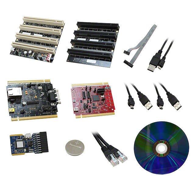
| 内容 | 板,电缆,LCD |
| 商标 | STMicroelectronics |
| 安装类型 | 固定 |
| 封装 | Bulk |
| 工具用于评估 | STM32F407ZG |
| 平台 | IAR KickStart Kit™ |
| 接口类型 | Audio, CAN, Ethernet, UART, UEXT, USB |
| 描述/功能 | For starting development with the STM32F4 series |
| 操作系统 | - |
| 数据总线宽度 | 32 bit |
| 板类型 | 评估平台 |
| 标准包装 | 1 |
| 核心 | ARM Cortex M4 |
| 核心处理器 | ARM® Cortex®-M4 |
| 特色产品 | http://www.digikey.com/product-highlights/cn/zh/stmicroelectronics-stm32/1369 |
| 用于 | STM32F4 |
| 类型 | MCU 32-位 |
| 系列 | STM3240G-SK/IAR |
| 配套使用产品/相关产品 | STM32F407 |


- 商务部:美国ITC正式对集成电路等产品启动337调查
- 曝三星4nm工艺存在良率问题 高通将骁龙8 Gen1或转产台积电
- 太阳诱电将投资9.5亿元在常州建新厂生产MLCC 预计2023年完工
- 英特尔发布欧洲新工厂建设计划 深化IDM 2.0 战略
- 台积电先进制程称霸业界 有大客户加持明年业绩稳了
- 达到5530亿美元!SIA预计今年全球半导体销售额将创下新高
- 英特尔拟将自动驾驶子公司Mobileye上市 估值或超500亿美元
- 三星加码芯片和SET,合并消费电子和移动部门,撤换高东真等 CEO
- 三星电子宣布重大人事变动 还合并消费电子和移动部门
- 海关总署:前11个月进口集成电路产品价值2.52万亿元 增长14.8%
PDF Datasheet 数据手册内容提取
STM32F405xx STM32F407xx ARM Cortex-M4 32b MCU+FPU, 210DMIPS, up to 1MB Flash/192+4KB RAM, USB OTG HS/FS, Ethernet, 17 TIMs, 3 ADCs, 15 comm. interfaces & camera Datasheet - production data Features • Core: ARM® 32-bit Cortex®-M4 CPU with FPU, (cid:38)(cid:34)(cid:39)(cid:33) Adaptive real-time accelerator (ART Accelerator™) allowing 0-wait state execution from Flash memory, frequency up to 168 MHz, memory protection unit, 210 DMIPS/ LQFP64 (10 × 10 mm) WLCSP90 UFBGA176 1.25 DMIPS/MHz (Dhrystone 2.1), and DSP LQFP100 (14 × 14 mm) (4.223x3.969mm) (10 × 10 mm) instructions LQFP144 (20 × 20 mm) LQFP176 (24 × 24 mm) • Memories • Up to 1 Mbyte of Flash memory • Up to 17 timers: up to twelve 16-bit and two 32- • Up to 192+4 Kbytes of SRAM including 64- bit timers up to 168 MHz, each with up to 4 Kbyte of CCM (core coupled memory) data IC/OC/PWM or pulse counter and quadrature RAM (incremental) encoder input • Flexible static memory controller supporting • Debug mode Compact Flash, SRAM, PSRAM, NOR and – Serial wire debug (SWD) & JTAG NAND memories interfaces • LCD parallel interface, 8080/6800 modes – Cortex-M4 Embedded Trace Macrocell™ • Clock, reset and supply management • Up to 140 I/O ports with interrupt capability – 1.8 V to 3.6 V application supply and I/Os – Up to 136 fast I/Os up to 84 MHz – POR, PDR, PVD and BOR – Up to 138 5 V-tolerant I/Os – 4-to-26 MHz crystal oscillator • Up to 15 communication interfaces – Internal 16 MHz factory-trimmed RC (1% – Up to 3 × I2C interfaces (SMBus/PMBus) accuracy) – Up to 4 USARTs/2 UARTs (10.5 Mbit/s, ISO – 32 kHz oscillator for RTC with calibration 7816 interface, LIN, IrDA, modem control) – Internal 32 kHz RC with calibration – Up to 3 SPIs (42 Mbits/s), 2 with muxed • Low-power operation full-duplex I2S to achieve audio class accuracy via internal audio PLL or external – Sleep, Stop and Standby modes clock – V supply for RTC, 20×32 bit backup BAT – 2 × CAN interfaces (2.0B Active) registers + optional 4 KB backup SRAM – SDIO interface • 3×12-bit, 2.4 MSPS A/D converters: up to 24 • Advanced connectivity channels and 7.2 MSPS in triple interleaved mode – USB 2.0 full-speed device/host/OTG controller with on-chip PHY • 2×12-bit D/A converters – USB 2.0 high-speed/full-speed • General-purpose DMA: 16-stream DMA device/host/OTG controller with dedicated controller with FIFOs and burst support DMA, on-chip full-speed PHY and ULPI – 10/100 Ethernet MAC with dedicated DMA: supports IEEE 1588v2 hardware, MII/RMII September 2016 DocID022152 Rev 8 1/202 This is information on a product in full production. www.st.com
STM32F405xx, STM32F407xx • 8- to 14-bit parallel camera interface up to • 96-bit unique ID 54 Mbytes/s • RTC: subsecond accuracy, hardware calendar • True random number generator • CRC calculation unit Table 1. Device summary Reference Part number STM32F405xx STM32F405RG, STM32F405VG, STM32F405ZG, STM32F405OG, STM32F405OE STM32F407VG, STM32F407IG, STM32F407ZG, STM32F407xx STM32F407VE, STM32F407ZE, STM32F407IE 2/202 DocID022152 Rev 8
STM32F405xx, STM32F407xx Contents Contents 1 Introduction . . . . . . . . . . . . . . . . . . . . . . . . . . . . . . . . . . . . . . . . . . . . . . . 12 2 Description . . . . . . . . . . . . . . . . . . . . . . . . . . . . . . . . . . . . . . . . . . . . . . . . 13 2.1 Full compatibility throughout the family . . . . . . . . . . . . . . . . . . . . . . . . . . 16 2.2 Device overview . . . . . . . . . . . . . . . . . . . . . . . . . . . . . . . . . . . . . . . . . . . . 19 2.2.1 ARM® Cortex®-M4 core with FPU and embedded Flash and SRAM . . 20 2.2.2 Adaptive real-time memory accelerator (ART Accelerator™) . . . . . . . . 20 2.2.3 Memory protection unit . . . . . . . . . . . . . . . . . . . . . . . . . . . . . . . . . . . . . 20 2.2.4 Embedded Flash memory . . . . . . . . . . . . . . . . . . . . . . . . . . . . . . . . . . . 20 2.2.5 CRC (cyclic redundancy check) calculation unit . . . . . . . . . . . . . . . . . . 21 2.2.6 Embedded SRAM . . . . . . . . . . . . . . . . . . . . . . . . . . . . . . . . . . . . . . . . . 21 2.2.7 Multi-AHB bus matrix . . . . . . . . . . . . . . . . . . . . . . . . . . . . . . . . . . . . . . . 21 2.2.8 DMA controller (DMA) . . . . . . . . . . . . . . . . . . . . . . . . . . . . . . . . . . . . . . 22 2.2.9 Flexible static memory controller (FSMC) . . . . . . . . . . . . . . . . . . . . . . . 23 2.2.10 Nested vectored interrupt controller (NVIC) . . . . . . . . . . . . . . . . . . . . . . 23 2.2.11 External interrupt/event controller (EXTI) . . . . . . . . . . . . . . . . . . . . . . . 23 2.2.12 Clocks and startup . . . . . . . . . . . . . . . . . . . . . . . . . . . . . . . . . . . . . . . . . 23 2.2.13 Boot modes . . . . . . . . . . . . . . . . . . . . . . . . . . . . . . . . . . . . . . . . . . . . . . 24 2.2.14 Power supply schemes . . . . . . . . . . . . . . . . . . . . . . . . . . . . . . . . . . . . . 24 2.2.15 Power supply supervisor . . . . . . . . . . . . . . . . . . . . . . . . . . . . . . . . . . . . 24 2.2.16 Voltage regulator . . . . . . . . . . . . . . . . . . . . . . . . . . . . . . . . . . . . . . . . . . 26 2.2.17 Regulator ON/OFF and internal reset ON/OFF availability . . . . . . . . . . 29 2.2.18 Real-time clock (RTC), backup SRAM and backup registers . . . . . . . . 29 2.2.19 Low-power modes . . . . . . . . . . . . . . . . . . . . . . . . . . . . . . . . . . . . . . . . . 30 2.2.20 V operation . . . . . . . . . . . . . . . . . . . . . . . . . . . . . . . . . . . . . . . . . . . . 31 BAT 2.2.21 Timers and watchdogs . . . . . . . . . . . . . . . . . . . . . . . . . . . . . . . . . . . . . . 31 2.2.22 Inter-integrated circuit interface (I²C) . . . . . . . . . . . . . . . . . . . . . . . . . . 34 2.2.23 Universal synchronous/asynchronous receiver transmitters (USART) . 34 2.2.24 Serial peripheral interface (SPI) . . . . . . . . . . . . . . . . . . . . . . . . . . . . . . . 35 2.2.25 Inter-integrated sound (I2S) . . . . . . . . . . . . . . . . . . . . . . . . . . . . . . . . . . 35 2.2.26 Audio PLL (PLLI2S) . . . . . . . . . . . . . . . . . . . . . . . . . . . . . . . . . . . . . . . . 36 2.2.27 Secure digital input/output interface (SDIO) . . . . . . . . . . . . . . . . . . . . . 36 2.2.28 Ethernet MAC interface with dedicated DMA and IEEE 1588 support . 36 2.2.29 Controller area network (bxCAN) . . . . . . . . . . . . . . . . . . . . . . . . . . . . . . 37 DocID022152 Rev 8 3/202
Contents STM32F405xx, STM32F407xx 2.2.30 Universal serial bus on-the-go full-speed (OTG_FS) . . . . . . . . . . . . . . . 37 2.2.31 Universal serial bus on-the-go high-speed (OTG_HS) . . . . . . . . . . . . . 38 2.2.32 Digital camera interface (DCMI) . . . . . . . . . . . . . . . . . . . . . . . . . . . . . . 38 2.2.33 Random number generator (RNG) . . . . . . . . . . . . . . . . . . . . . . . . . . . . 38 2.2.34 General-purpose input/outputs (GPIOs) . . . . . . . . . . . . . . . . . . . . . . . . 38 2.2.35 Analog-to-digital converters (ADCs) . . . . . . . . . . . . . . . . . . . . . . . . . . . 39 2.2.36 Temperature sensor . . . . . . . . . . . . . . . . . . . . . . . . . . . . . . . . . . . . . . . . 39 2.2.37 Digital-to-analog converter (DAC) . . . . . . . . . . . . . . . . . . . . . . . . . . . . . 39 2.2.38 Serial wire JTAG debug port (SWJ-DP) . . . . . . . . . . . . . . . . . . . . . . . . . 40 2.2.39 Embedded Trace Macrocell™ . . . . . . . . . . . . . . . . . . . . . . . . . . . . . . . . 40 3 Pinouts and pin description . . . . . . . . . . . . . . . . . . . . . . . . . . . . . . . . . . 41 4 Memory mapping . . . . . . . . . . . . . . . . . . . . . . . . . . . . . . . . . . . . . . . . . . . 71 5 Electrical characteristics . . . . . . . . . . . . . . . . . . . . . . . . . . . . . . . . . . . . 76 5.1 Parameter conditions . . . . . . . . . . . . . . . . . . . . . . . . . . . . . . . . . . . . . . . . 76 5.1.1 Minimum and maximum values . . . . . . . . . . . . . . . . . . . . . . . . . . . . . . . 76 5.1.2 Typical values . . . . . . . . . . . . . . . . . . . . . . . . . . . . . . . . . . . . . . . . . . . . 76 5.1.3 Typical curves . . . . . . . . . . . . . . . . . . . . . . . . . . . . . . . . . . . . . . . . . . . . 76 5.1.4 Loading capacitor . . . . . . . . . . . . . . . . . . . . . . . . . . . . . . . . . . . . . . . . . 76 5.1.5 Pin input voltage . . . . . . . . . . . . . . . . . . . . . . . . . . . . . . . . . . . . . . . . . . 76 5.1.6 Power supply scheme . . . . . . . . . . . . . . . . . . . . . . . . . . . . . . . . . . . . . . 77 5.1.7 Current consumption measurement . . . . . . . . . . . . . . . . . . . . . . . . . . . 78 5.2 Absolute maximum ratings . . . . . . . . . . . . . . . . . . . . . . . . . . . . . . . . . . . . 78 5.3 Operating conditions . . . . . . . . . . . . . . . . . . . . . . . . . . . . . . . . . . . . . . . . 79 5.3.1 General operating conditions . . . . . . . . . . . . . . . . . . . . . . . . . . . . . . . . . 79 5.3.2 VCAP_1/VCAP_2 external capacitor . . . . . . . . . . . . . . . . . . . . . . . . . . . 82 5.3.3 Operating conditions at power-up / power-down (regulator ON) . . . . . . 82 5.3.4 Operating conditions at power-up / power-down (regulator OFF) . . . . . 82 5.3.5 Embedded reset and power control block characteristics . . . . . . . . . . . 83 5.3.6 Supply current characteristics . . . . . . . . . . . . . . . . . . . . . . . . . . . . . . . . 84 5.3.7 Wakeup time from low-power mode . . . . . . . . . . . . . . . . . . . . . . . . . . . 98 5.3.8 External clock source characteristics . . . . . . . . . . . . . . . . . . . . . . . . . . . 99 5.3.9 Internal clock source characteristics . . . . . . . . . . . . . . . . . . . . . . . . . . 103 5.3.10 PLL characteristics . . . . . . . . . . . . . . . . . . . . . . . . . . . . . . . . . . . . . . . 104 5.3.11 PLL spread spectrum clock generation (SSCG) characteristics . . . . . 106 4/202 DocID022152 Rev 8
STM32F405xx, STM32F407xx Contents 5.3.12 Memory characteristics . . . . . . . . . . . . . . . . . . . . . . . . . . . . . . . . . . . . 108 5.3.13 EMC characteristics . . . . . . . . . . . . . . . . . . . . . . . . . . . . . . . . . . . . . . . 110 5.3.14 Absolute maximum ratings (electrical sensitivity) . . . . . . . . . . . . . . . . 112 5.3.15 I/O current injection characteristics . . . . . . . . . . . . . . . . . . . . . . . . . . . 113 5.3.16 I/O port characteristics . . . . . . . . . . . . . . . . . . . . . . . . . . . . . . . . . . . . . 114 5.3.17 NRST pin characteristics . . . . . . . . . . . . . . . . . . . . . . . . . . . . . . . . . . . 118 5.3.18 TIM timer characteristics . . . . . . . . . . . . . . . . . . . . . . . . . . . . . . . . . . . 119 5.3.19 Communications interfaces . . . . . . . . . . . . . . . . . . . . . . . . . . . . . . . . . 121 5.3.20 CAN (controller area network) interface . . . . . . . . . . . . . . . . . . . . . . . 133 5.3.21 12-bit ADC characteristics . . . . . . . . . . . . . . . . . . . . . . . . . . . . . . . . . . 133 5.3.22 Temperature sensor characteristics . . . . . . . . . . . . . . . . . . . . . . . . . . . 138 5.3.23 V monitoring characteristics . . . . . . . . . . . . . . . . . . . . . . . . . . . . . . 139 BAT 5.3.24 Embedded reference voltage . . . . . . . . . . . . . . . . . . . . . . . . . . . . . . . . 139 5.3.25 DAC electrical characteristics . . . . . . . . . . . . . . . . . . . . . . . . . . . . . . . 139 5.3.26 FSMC characteristics . . . . . . . . . . . . . . . . . . . . . . . . . . . . . . . . . . . . . . 142 5.3.27 Camera interface (DCMI) timing specifications . . . . . . . . . . . . . . . . . . 161 5.3.28 SD/SDIO MMC card host interface (SDIO) characteristics . . . . . . . . . 162 5.3.29 RTC characteristics . . . . . . . . . . . . . . . . . . . . . . . . . . . . . . . . . . . . . . . 163 6 Package information . . . . . . . . . . . . . . . . . . . . . . . . . . . . . . . . . . . . . . . 164 6.1 WLCSP90 package information . . . . . . . . . . . . . . . . . . . . . . . . . . . . . . . 164 6.2 LQFP64 package information . . . . . . . . . . . . . . . . . . . . . . . . . . . . . . . . . 167 6.3 LQPF100 package information . . . . . . . . . . . . . . . . . . . . . . . . . . . . . . . . 170 6.4 LQFP144 package information . . . . . . . . . . . . . . . . . . . . . . . . . . . . . . . . 173 6.5 UFBGA176+25 package information . . . . . . . . . . . . . . . . . . . . . . . . . . . 177 6.6 LQFP176 package information . . . . . . . . . . . . . . . . . . . . . . . . . . . . . . . . 180 6.7 Thermal characteristics . . . . . . . . . . . . . . . . . . . . . . . . . . . . . . . . . . . . . 184 7 Part numbering . . . . . . . . . . . . . . . . . . . . . . . . . . . . . . . . . . . . . . . . . . . 185 Appendix A Application block diagrams . . . . . . . . . . . . . . . . . . . . . . . . . . . . . . 186 A.1 USB OTG full speed (FS) interface solutions . . . . . . . . . . . . . . . . . . . . . 186 A.2 USB OTG high speed (HS) interface solutions. . . . . . . . . . . . . . . . . . . . 188 A.3 Ethernet interface solutions. . . . . . . . . . . . . . . . . . . . . . . . . . . . . . . . . . . 189 8 Revision history . . . . . . . . . . . . . . . . . . . . . . . . . . . . . . . . . . . . . . . . . . 191 DocID022152 Rev 8 5/202
List of tables STM32F405xx, STM32F407xx List of tables Table 1. Device summary. . . . . . . . . . . . . . . . . . . . . . . . . . . . . . . . . . . . . . . . . . . . . . . . . . . . . . . . . . 2 Table 2. STM32F405xx and STM32F407xx: features and peripheral counts. . . . . . . . . . . . . . . . . . 14 Table 3. Regulator ON/OFF and internal reset ON/OFF availability. . . . . . . . . . . . . . . . . . . . . . . . . 29 Table 4. Timer feature comparison. . . . . . . . . . . . . . . . . . . . . . . . . . . . . . . . . . . . . . . . . . . . . . . . . . 31 Table 5. USART feature comparison . . . . . . . . . . . . . . . . . . . . . . . . . . . . . . . . . . . . . . . . . . . . . . . . 35 Table 6. Legend/abbreviations used in the pinout table. . . . . . . . . . . . . . . . . . . . . . . . . . . . . . . . . . 46 Table 7. STM32F40xxx pin and ball definitions . . . . . . . . . . . . . . . . . . . . . . . . . . . . . . . . . . . . . . . . 47 Table 8. FSMC pin definition . . . . . . . . . . . . . . . . . . . . . . . . . . . . . . . . . . . . . . . . . . . . . . . . . . . . . . 59 Table 9. Alternate function mapping. . . . . . . . . . . . . . . . . . . . . . . . . . . . . . . . . . . . . . . . . . . . . . . . . 62 Table 10. register boundary addresses. . . . . . . . . . . . . . . . . . . . . . . . . . . . . . . . . . . . . . . . . . . . . . . 72 Table 11. Voltage characteristics . . . . . . . . . . . . . . . . . . . . . . . . . . . . . . . . . . . . . . . . . . . . . . . . . . . . 78 Table 12. Current characteristics . . . . . . . . . . . . . . . . . . . . . . . . . . . . . . . . . . . . . . . . . . . . . . . . . . . . 79 Table 13. Thermal characteristics. . . . . . . . . . . . . . . . . . . . . . . . . . . . . . . . . . . . . . . . . . . . . . . . . . . . 79 Table 14. General operating conditions . . . . . . . . . . . . . . . . . . . . . . . . . . . . . . . . . . . . . . . . . . . . . . . 79 Table 15. Limitations depending on the operating power supply range. . . . . . . . . . . . . . . . . . . . . . . 81 Table 16. VCAP_1/VCAP_2 operating conditions . . . . . . . . . . . . . . . . . . . . . . . . . . . . . . . . . . . . . . . 82 Table 17. Operating conditions at power-up / power-down (regulator ON) . . . . . . . . . . . . . . . . . . . . 82 Table 18. Operating conditions at power-up / power-down (regulator OFF). . . . . . . . . . . . . . . . . . . . 82 Table 19. Embedded reset and power control block characteristics. . . . . . . . . . . . . . . . . . . . . . . . . . 83 Table 20. Typical and maximum current consumption in Run mode, code with data processing running from Flash memory (ART accelerator enabled) or RAM . . . . . . . . . . . . . . . . . . . 85 Table 21. Typical and maximum current consumption in Run mode, code with data processing running from Flash memory (ART accelerator disabled). . . . . . . . . . . . . . . . . . . . . . . . . . 86 Table 22. Typical and maximum current consumption in Sleep mode. . . . . . . . . . . . . . . . . . . . . . . . 89 Table 23. Typical and maximum current consumptions in Stop mode. . . . . . . . . . . . . . . . . . . . . . . . 90 Table 24. Typical and maximum current consumptions in Standby mode . . . . . . . . . . . . . . . . . . . . . 90 Table 25. Typical and maximum current consumptions in V mode. . . . . . . . . . . . . . . . . . . . . . . . 91 BAT Table 26. Typical current consumption in Run mode, code with data processing running from Flash memory, regulator ON (ART accelerator enabled except prefetch), V = 1.8 V. . . . . . . . . . . . . . . . . . . . . . . . . . . . . . . . . . . . . . . . . . . . . . . 93 DD Table 27. Switching output I/O current consumption . . . . . . . . . . . . . . . . . . . . . . . . . . . . . . . . . . . . . 95 Table 28. Peripheral current consumption . . . . . . . . . . . . . . . . . . . . . . . . . . . . . . . . . . . . . . . . . . . . . 96 Table 29. Low-power mode wakeup timings . . . . . . . . . . . . . . . . . . . . . . . . . . . . . . . . . . . . . . . . . . . 99 Table 30. High-speed external user clock characteristics. . . . . . . . . . . . . . . . . . . . . . . . . . . . . . . . . . 99 Table 31. Low-speed external user clock characteristics. . . . . . . . . . . . . . . . . . . . . . . . . . . . . . . . . 100 Table 32. HSE 4-26 MHz oscillator characteristics . . . . . . . . . . . . . . . . . . . . . . . . . . . . . . . . . . . . . 101 Table 33. LSE oscillator characteristics (f = 32.768 kHz) . . . . . . . . . . . . . . . . . . . . . . . . . . . . . . 102 LSE Table 34. HSI oscillator characteristics . . . . . . . . . . . . . . . . . . . . . . . . . . . . . . . . . . . . . . . . . . . . . . 103 Table 35. LSI oscillator characteristics . . . . . . . . . . . . . . . . . . . . . . . . . . . . . . . . . . . . . . . . . . . . . . 103 Table 36. Main PLL characteristics. . . . . . . . . . . . . . . . . . . . . . . . . . . . . . . . . . . . . . . . . . . . . . . . . . 104 Table 37. PLLI2S (audio PLL) characteristics . . . . . . . . . . . . . . . . . . . . . . . . . . . . . . . . . . . . . . . . . 105 Table 38. SSCG parameters constraint . . . . . . . . . . . . . . . . . . . . . . . . . . . . . . . . . . . . . . . . . . . . . . 106 Table 39. Flash memory characteristics. . . . . . . . . . . . . . . . . . . . . . . . . . . . . . . . . . . . . . . . . . . . . . 108 Table 40. Flash memory programming. . . . . . . . . . . . . . . . . . . . . . . . . . . . . . . . . . . . . . . . . . . . . . . 108 Table 41. Flash memory programming with VPP. . . . . . . . . . . . . . . . . . . . . . . . . . . . . . . . . . . . . . . 110 Table 42. Flash memory endurance and data retention. . . . . . . . . . . . . . . . . . . . . . . . . . . . . . . . . . 110 Table 43. EMS characteristics . . . . . . . . . . . . . . . . . . . . . . . . . . . . . . . . . . . . . . . . . . . . . . . . . . . . . 111 Table 44. EMI characteristics. . . . . . . . . . . . . . . . . . . . . . . . . . . . . . . . . . . . . . . . . . . . . . . . . . . . . . 112 6/202 DocID022152 Rev 8
STM32F405xx, STM32F407xx List of tables Table 45. ESD absolute maximum ratings. . . . . . . . . . . . . . . . . . . . . . . . . . . . . . . . . . . . . . . . . . . . 112 Table 46. Electrical sensitivities . . . . . . . . . . . . . . . . . . . . . . . . . . . . . . . . . . . . . . . . . . . . . . . . . . . . 113 Table 47. I/O current injection susceptibility. . . . . . . . . . . . . . . . . . . . . . . . . . . . . . . . . . . . . . . . . . . 114 Table 48. I/O static characteristics . . . . . . . . . . . . . . . . . . . . . . . . . . . . . . . . . . . . . . . . . . . . . . . . . . 114 Table 49. Output voltage characteristics . . . . . . . . . . . . . . . . . . . . . . . . . . . . . . . . . . . . . . . . . . . . . 116 Table 50. I/O AC characteristics. . . . . . . . . . . . . . . . . . . . . . . . . . . . . . . . . . . . . . . . . . . . . . . . . . . . 117 Table 51. NRST pin characteristics . . . . . . . . . . . . . . . . . . . . . . . . . . . . . . . . . . . . . . . . . . . . . . . . . 119 Table 52. Characteristics of TIMx connected to the APB1 domain . . . . . . . . . . . . . . . . . . . . . . . . . 120 Table 53. Characteristics of TIMx connected to the APB2 domain . . . . . . . . . . . . . . . . . . . . . . . . . 121 Table 54. I2C analog filter characteristics. . . . . . . . . . . . . . . . . . . . . . . . . . . . . . . . . . . . . . . . . . . . . 121 Table 55. SPI dynamic characteristics . . . . . . . . . . . . . . . . . . . . . . . . . . . . . . . . . . . . . . . . . . . . . . . 122 Table 56. I2S dynamic characteristics . . . . . . . . . . . . . . . . . . . . . . . . . . . . . . . . . . . . . . . . . . . . . . . 126 Table 57. USB OTG FS startup time . . . . . . . . . . . . . . . . . . . . . . . . . . . . . . . . . . . . . . . . . . . . . . . . 128 Table 58. USB OTG FS DC electrical characteristics. . . . . . . . . . . . . . . . . . . . . . . . . . . . . . . . . . . . 128 Table 59. USB OTG FS electrical characteristics. . . . . . . . . . . . . . . . . . . . . . . . . . . . . . . . . . . . . . . 129 Table 60. USB HS DC electrical characteristics. . . . . . . . . . . . . . . . . . . . . . . . . . . . . . . . . . . . . . . . 129 Table 61. USB HS clock timing parameters. . . . . . . . . . . . . . . . . . . . . . . . . . . . . . . . . . . . . . . . . . . 129 Table 62. ULPI timing. . . . . . . . . . . . . . . . . . . . . . . . . . . . . . . . . . . . . . . . . . . . . . . . . . . . . . . . . . . . 130 Table 63. Ethernet DC electrical characteristics. . . . . . . . . . . . . . . . . . . . . . . . . . . . . . . . . . . . . . . . 131 Table 64. Dynamic characteristics: Eternity MAC signals for SMI . . . . . . . . . . . . . . . . . . . . . . . . . . 131 Table 65. Dynamic characteristics: Ethernet MAC signals for RMII. . . . . . . . . . . . . . . . . . . . . . . . . 132 Table 66. Dynamic characteristics: Ethernet MAC signals for MII . . . . . . . . . . . . . . . . . . . . . . . . . . 133 Table 67. ADC characteristics . . . . . . . . . . . . . . . . . . . . . . . . . . . . . . . . . . . . . . . . . . . . . . . . . . . . . 133 Table 68. ADC accuracy at f = 30 MHz . . . . . . . . . . . . . . . . . . . . . . . . . . . . . . . . . . . . . . . . . . . 135 ADC Table 69. Temperature sensor characteristics. . . . . . . . . . . . . . . . . . . . . . . . . . . . . . . . . . . . . . . . . 138 Table 70. Temperature sensor calibration values. . . . . . . . . . . . . . . . . . . . . . . . . . . . . . . . . . . . . . . 138 Table 71. V monitoring characteristics . . . . . . . . . . . . . . . . . . . . . . . . . . . . . . . . . . . . . . . . . . . . 139 BAT Table 72. Embedded internal reference voltage. . . . . . . . . . . . . . . . . . . . . . . . . . . . . . . . . . . . . . . . 139 Table 73. Internal reference voltage calibration values . . . . . . . . . . . . . . . . . . . . . . . . . . . . . . . . . . 139 Table 74. DAC characteristics . . . . . . . . . . . . . . . . . . . . . . . . . . . . . . . . . . . . . . . . . . . . . . . . . . . . . 139 Table 75. Asynchronous non-multiplexed SRAM/PSRAM/NOR read timings . . . . . . . . . . . . . . . . . 143 Table 76. Asynchronous non-multiplexed SRAM/PSRAM/NOR write timings . . . . . . . . . . . . . . . . . 144 Table 77. Asynchronous multiplexed PSRAM/NOR read timings. . . . . . . . . . . . . . . . . . . . . . . . . . . 145 Table 78. Asynchronous multiplexed PSRAM/NOR write timings . . . . . . . . . . . . . . . . . . . . . . . . . . 146 Table 79. Synchronous multiplexed NOR/PSRAM read timings . . . . . . . . . . . . . . . . . . . . . . . . . . . 148 Table 80. Synchronous multiplexed PSRAM write timings. . . . . . . . . . . . . . . . . . . . . . . . . . . . . . . . 149 Table 81. Synchronous non-multiplexed NOR/PSRAM read timings. . . . . . . . . . . . . . . . . . . . . . . . 151 Table 82. Synchronous non-multiplexed PSRAM write timings . . . . . . . . . . . . . . . . . . . . . . . . . . . . 152 Table 83. Switching characteristics for PC Card/CF read and write cycles in attribute/common space. . . . . . . . . . . . . . . . . . . . . . . . . . . . . . . . . . . . . . . . . . . . . . . . 157 Table 84. Switching characteristics for PC Card/CF read and write cycles in I/O space . . . . . . . . . . . . . . . . . . . . . . . . . . . . . . . . . . . . . . . . . . . . . . . . . . . . . . . . . . . 158 Table 85. Switching characteristics for NAND Flash read cycles. . . . . . . . . . . . . . . . . . . . . . . . . . . 160 Table 86. Switching characteristics for NAND Flash write cycles. . . . . . . . . . . . . . . . . . . . . . . . . . . 161 Table 87. DCMI characteristics. . . . . . . . . . . . . . . . . . . . . . . . . . . . . . . . . . . . . . . . . . . . . . . . . . . . . 161 Table 88. Dynamic characteristics: SD / MMC characteristics. . . . . . . . . . . . . . . . . . . . . . . . . . . . . 163 Table 89. RTC characteristics . . . . . . . . . . . . . . . . . . . . . . . . . . . . . . . . . . . . . . . . . . . . . . . . . . . . . 163 Table 90. WLCSP90 - 4.223 x 3.969 mm, 0.400 mm pitch wafer level chip scale package mechanical data. . . . . . . . . . . . . . . . . . . . . . . . . . . . . . . . . . . . . . . . . . . . . . . . . 165 Table 91. WLCSP90 recommended PCB design rules . . . . . . . . . . . . . . . . . . . . . . . . . . . . . . . . . . 166 Table 92. LQFP64 – 64-pin 10 x 10 mm low-profile quad flat package mechanical data . . . . . . . . . . . . . . . . . . . . . . . . . . . . . . . . . . . . . . . . . . . . . . . . . . . . . . . . 167 DocID022152 Rev 8 7/202
List of tables STM32F405xx, STM32F407xx Table 93. LQPF100 – 100-pin, 14 x 14 mm low-profile quad flat package mechanical data . . . . . . . . . . . . . . . . . . . . . . . . . . . . . . . . . . . . . . . . . . . . . . . . . . . . . . . . 170 Table 94. LQFP144 - 144-pin, 20 x 20 mm low-profile quad flat package mechanical data . . . . . . . . . . . . . . . . . . . . . . . . . . . . . . . . . . . . . . . . . . . . . . . . . . . . . . . . 174 Table 95. UFBGA176+25 ball, 10 × 10 × 0.65 mm pitch, ultra thin fine pitch ball grid array mechanical data. . . . . . . . . . . . . . . . . . . . . . . . . . . . . . . . . . . . . . . . . . . . . 177 Table 96. UFBGA176+2 recommended PCB design rules (0.65 mm pitch BGA) . . . . . . . . . . . . . . 178 Table 97. LQFP176 - 176-pin, 24 x 24 mm low profile quad flat package mechanical data . . . . . . . . . . . . . . . . . . . . . . . . . . . . . . . . . . . . . . . . . . . . . . . . . . . . . . . . 180 Table 98. Package thermal characteristics. . . . . . . . . . . . . . . . . . . . . . . . . . . . . . . . . . . . . . . . . . . . 184 Table 99. Ordering information scheme. . . . . . . . . . . . . . . . . . . . . . . . . . . . . . . . . . . . . . . . . . . . . . 185 Table 100. Document revision history . . . . . . . . . . . . . . . . . . . . . . . . . . . . . . . . . . . . . . . . . . . . . . . . 191 8/202 DocID022152 Rev 8
STM32F405xx, STM32F407xx List of figures List of figures Figure 1. Compatible board design between STM32F10xx/STM32F40xxx for LQFP64. . . . . . . . . . 16 Figure 2. Compatible board design STM32F10xx/STM32F2/STM32F40xxx for LQFP100 package. . . . . . . . . . . . . . . . . . . . . . . . . . . . . . . . . . . . . . . . . . . . . . . . . . . . . 17 Figure 3. Compatible board design between STM32F10xx/STM32F2/STM32F40xxx for LQFP144 package. . . . . . . . . . . . . . . . . . . . . . . . . . . . . . . . . . . . . . . . . . . . . . . . . . . . . 17 Figure 4. Compatible board design between STM32F2 and STM32F40xxx for LQFP176 and BGA176 packages . . . . . . . . . . . . . . . . . . . . . . . . . . . . . . . . . . . . . . . . 18 Figure 5. STM32F40xxx block diagram. . . . . . . . . . . . . . . . . . . . . . . . . . . . . . . . . . . . . . . . . . . . . . . 19 Figure 6. Multi-AHB matrix. . . . . . . . . . . . . . . . . . . . . . . . . . . . . . . . . . . . . . . . . . . . . . . . . . . . . . . . . 22 Figure 7. Power supply supervisor interconnection with internal reset OFF . . . . . . . . . . . . . . . . . . . 25 Figure 8. PDR_ON and NRST control with internal reset OFF . . . . . . . . . . . . . . . . . . . . . . . . . . . . . 26 Figure 9. Regulator OFF . . . . . . . . . . . . . . . . . . . . . . . . . . . . . . . . . . . . . . . . . . . . . . . . . . . . . . . . . . 27 Figure 10. Startup in regulator OFF mode: slow V slope DD - power-down reset risen after V /V stabilization. . . . . . . . . . . . . . . . . . . . . . . . 28 CAP_1 CAP_2 Figure 11. Startup in regulator OFF mode: fast V slope DD - power-down reset risen before V /V stabilization . . . . . . . . . . . . . . . . . . . . . . 29 CAP_1 CAP_2 Figure 12. STM32F40xxx LQFP64 pinout. . . . . . . . . . . . . . . . . . . . . . . . . . . . . . . . . . . . . . . . . . . . . . 41 Figure 13. STM32F40xxx LQFP100 pinout. . . . . . . . . . . . . . . . . . . . . . . . . . . . . . . . . . . . . . . . . . . . . 42 Figure 14. STM32F40xxx LQFP144 pinout. . . . . . . . . . . . . . . . . . . . . . . . . . . . . . . . . . . . . . . . . . . . . 43 Figure 15. STM32F40xxx LQFP176 pinout. . . . . . . . . . . . . . . . . . . . . . . . . . . . . . . . . . . . . . . . . . . . . 44 Figure 16. STM32F40xxx UFBGA176 ballout . . . . . . . . . . . . . . . . . . . . . . . . . . . . . . . . . . . . . . . . . . . 45 Figure 17. STM32F40xxx WLCSP90 ballout. . . . . . . . . . . . . . . . . . . . . . . . . . . . . . . . . . . . . . . . . . . . 46 Figure 18. STM32F40xxx memory map. . . . . . . . . . . . . . . . . . . . . . . . . . . . . . . . . . . . . . . . . . . . . . . . 71 Figure 19. Pin loading conditions. . . . . . . . . . . . . . . . . . . . . . . . . . . . . . . . . . . . . . . . . . . . . . . . . . . . . 76 Figure 20. Pin input voltage. . . . . . . . . . . . . . . . . . . . . . . . . . . . . . . . . . . . . . . . . . . . . . . . . . . . . . . . . 76 Figure 21. Power supply scheme . . . . . . . . . . . . . . . . . . . . . . . . . . . . . . . . . . . . . . . . . . . . . . . . . . . . 77 Figure 22. Current consumption measurement scheme . . . . . . . . . . . . . . . . . . . . . . . . . . . . . . . . . . . 78 Figure 23. External capacitor C . . . . . . . . . . . . . . . . . . . . . . . . . . . . . . . . . . . . . . . . . . . . . . . . . . . 82 EXT Figure 24. Typical current consumption versus temperature, Run mode, code with data processing running from Flash (ART accelerator ON) or RAM, and peripherals OFF . . . . 87 Figure 25. Typical current consumption versus temperature, Run mode, code with data processing running from Flash (ART accelerator ON) or RAM, and peripherals ON. . . . . 87 Figure 26. Typical current consumption versus temperature, Run mode, code with data processing running from Flash (ART accelerator OFF) or RAM, and peripherals OFF . . . 88 Figure 27. Typical current consumption versus temperature, Run mode, code with data processing running from Flash (ART accelerator OFF) or RAM, and peripherals ON . . . . 88 Figure 28. Typical V current consumption (LSE and RTC ON/backup RAM OFF) . . . . . . . . . . . . 91 BAT Figure 29. Typical V current consumption (LSE and RTC ON/backup RAM ON) . . . . . . . . . . . . . 92 BAT Figure 30. High-speed external clock source AC timing diagram . . . . . . . . . . . . . . . . . . . . . . . . . . . 100 Figure 31. Low-speed external clock source AC timing diagram. . . . . . . . . . . . . . . . . . . . . . . . . . . . 101 Figure 32. Typical application with an 8 MHz crystal. . . . . . . . . . . . . . . . . . . . . . . . . . . . . . . . . . . . . 102 Figure 33. Typical application with a 32.768 kHz crystal. . . . . . . . . . . . . . . . . . . . . . . . . . . . . . . . . . 103 Figure 34. ACC versus temperature . . . . . . . . . . . . . . . . . . . . . . . . . . . . . . . . . . . . . . . . . . . . . . . 104 LSI Figure 35. PLL output clock waveforms in center spread mode . . . . . . . . . . . . . . . . . . . . . . . . . . . . 107 Figure 36. PLL output clock waveforms in down spread mode. . . . . . . . . . . . . . . . . . . . . . . . . . . . . 108 Figure 37. I/O AC characteristics definition . . . . . . . . . . . . . . . . . . . . . . . . . . . . . . . . . . . . . . . . . . . . 118 Figure 38. Recommended NRST pin protection . . . . . . . . . . . . . . . . . . . . . . . . . . . . . . . . . . . . . . . . 119 Figure 39. SPI timing diagram - slave mode and CPHA = 0 . . . . . . . . . . . . . . . . . . . . . . . . . . . . . . . 124 DocID022152 Rev 8 9/202
List of figures STM32F405xx, STM32F407xx Figure 40. SPI timing diagram - slave mode and CPHA = 1 . . . . . . . . . . . . . . . . . . . . . . . . . . . . . . . 124 Figure 41. SPI timing diagram - master mode. . . . . . . . . . . . . . . . . . . . . . . . . . . . . . . . . . . . . . . . . . 125 Figure 42. I2S slave timing diagram (Philips protocol) . . . . . . . . . . . . . . . . . . . . . . . . . . . . . . . . . . . 127 Figure 43. I2S master timing diagram (Philips protocol)(1). . . . . . . . . . . . . . . . . . . . . . . . . . . . . . . . . 127 Figure 44. USB OTG FS timings: definition of data signal rise and fall time . . . . . . . . . . . . . . . . . . . 129 Figure 45. ULPI timing diagram. . . . . . . . . . . . . . . . . . . . . . . . . . . . . . . . . . . . . . . . . . . . . . . . . . . . . 130 Figure 46. Ethernet SMI timing diagram . . . . . . . . . . . . . . . . . . . . . . . . . . . . . . . . . . . . . . . . . . . . . . 131 Figure 47. Ethernet RMII timing diagram. . . . . . . . . . . . . . . . . . . . . . . . . . . . . . . . . . . . . . . . . . . . . . 132 Figure 48. Ethernet MII timing diagram . . . . . . . . . . . . . . . . . . . . . . . . . . . . . . . . . . . . . . . . . . . . . . . 132 Figure 49. ADC accuracy characteristics. . . . . . . . . . . . . . . . . . . . . . . . . . . . . . . . . . . . . . . . . . . . . . 136 Figure 50. Typical connection diagram using the ADC . . . . . . . . . . . . . . . . . . . . . . . . . . . . . . . . . . . 136 Figure 51. Power supply and reference decoupling (V not connected to V ). . . . . . . . . . . . . 137 REF+ DDA Figure 52. Power supply and reference decoupling (V connected to V ). . . . . . . . . . . . . . . . 138 REF+ DDA Figure 53. 12-bit buffered /non-buffered DAC . . . . . . . . . . . . . . . . . . . . . . . . . . . . . . . . . . . . . . . . . . 142 Figure 54. Asynchronous non-multiplexed SRAM/PSRAM/NOR read waveforms . . . . . . . . . . . . . . 143 Figure 55. Asynchronous non-multiplexed SRAM/PSRAM/NOR write waveforms . . . . . . . . . . . . . . 144 Figure 56. Asynchronous multiplexed PSRAM/NOR read waveforms. . . . . . . . . . . . . . . . . . . . . . . . 145 Figure 57. Asynchronous multiplexed PSRAM/NOR write waveforms . . . . . . . . . . . . . . . . . . . . . . . 146 Figure 58. Synchronous multiplexed NOR/PSRAM read timings . . . . . . . . . . . . . . . . . . . . . . . . . . . 147 Figure 59. Synchronous multiplexed PSRAM write timings. . . . . . . . . . . . . . . . . . . . . . . . . . . . . . . . 149 Figure 60. Synchronous non-multiplexed NOR/PSRAM read timings. . . . . . . . . . . . . . . . . . . . . . . . 150 Figure 61. Synchronous non-multiplexed PSRAM write timings . . . . . . . . . . . . . . . . . . . . . . . . . . . . 152 Figure 62. PC Card/CompactFlash controller waveforms for common memory read access. . . . . . 153 Figure 63. PC Card/CompactFlash controller waveforms for common memory write access. . . . . . 154 Figure 64. PC Card/CompactFlash controller waveforms for attribute memory read access. . . . . . . . . . . . . . . . . . . . . . . . . . . . . . . . . . . . . . . . . . . . . . . . . . . . . . . . . . . . . . . . 155 Figure 65. PC Card/CompactFlash controller waveforms for attribute memory write access. . . . . . . . . . . . . . . . . . . . . . . . . . . . . . . . . . . . . . . . . . . . . . . . . . . . . . . . . . . . . . . . 156 Figure 66. PC Card/CompactFlash controller waveforms for I/O space read access . . . . . . . . . . . . 156 Figure 67. PC Card/CompactFlash controller waveforms for I/O space write access. . . . . . . . . . . . 157 Figure 68. NAND controller waveforms for read access . . . . . . . . . . . . . . . . . . . . . . . . . . . . . . . . . . 159 Figure 69. NAND controller waveforms for write access . . . . . . . . . . . . . . . . . . . . . . . . . . . . . . . . . . 159 Figure 70. NAND controller waveforms for common memory read access. . . . . . . . . . . . . . . . . . . . 160 Figure 71. NAND controller waveforms for common memory write access. . . . . . . . . . . . . . . . . . . . 160 Figure 72. DCMI timing diagram . . . . . . . . . . . . . . . . . . . . . . . . . . . . . . . . . . . . . . . . . . . . . . . . . . . . 161 Figure 73. SDIO high-speed mode . . . . . . . . . . . . . . . . . . . . . . . . . . . . . . . . . . . . . . . . . . . . . . . . . . 162 Figure 74. SD default mode. . . . . . . . . . . . . . . . . . . . . . . . . . . . . . . . . . . . . . . . . . . . . . . . . . . . . . . . 163 Figure 75. WLCSP90 - 4.223 x 3.969 mm, 0.400 mm pitch wafer level chip scale package outline. . . . . . . . . . . . . . . . . . . . . . . . . . . . . . . . . . . . . . . . . . . . . . . . . . . . . . . . . 164 Figure 76. WLCSP90 - 4.223 x 3.969 mm, 0.400 mm pitch wafer level chip scale recommended footprint. . . . . . . . . . . . . . . . . . . . . . . . . . . . . . . . . . . . . . . . . . . . . . . . . . . 165 Figure 77. WLCSP90 marking example (package top view) . . . . . . . . . . . . . . . . . . . . . . . . . . . . . . . 166 Figure 78. LQFP64 – 64-pin, 10 x 10 mm low-profile quad flat package outline. . . . . . . . . . . . . . . . 167 Figure 79. LQFP64 – 64-pin, 10 x 10 mm low-profile quad flat package recommended footprint. . . . . . . . . . . . . . . . . . . . . . . . . . . . . . . . . . . . . . . . . . . . . . . . . . . 168 Figure 80. LPQF64 marking example (package top view) . . . . . . . . . . . . . . . . . . . . . . . . . . . . . . . . 169 Figure 81. LQFP100 - 100-pin, 14 x 14 mm low-profile quad flat package outline . . . . . . . . . . . . . . 170 Figure 82. LQFP100 - 100-pin, 14 x 14 mm low-profile quad flat recommended footprint. . . . . . . . . . . . . . . . . . . . . . . . . . . . . . . . . . . . . . . . . . . . . . . . . . . 171 Figure 83. LQFP100 marking example (package top view) . . . . . . . . . . . . . . . . . . . . . . . . . . . . . . . 172 Figure 84. LQFP144 - 144-pin, 20 x 20 mm low-profile quad flat package outline . . . . . . . . . . . . . . 173 Figure 85. LQFP144 - 144-pin,20 x 20 mm low-profile quad flat package 10/202 DocID022152 Rev 8
STM32F405xx, STM32F407xx List of figures recommended footprint. . . . . . . . . . . . . . . . . . . . . . . . . . . . . . . . . . . . . . . . . . . . . . . . . . . 175 Figure 86. LQFP144 marking example (package top view) . . . . . . . . . . . . . . . . . . . . . . . . . . . . . . . 176 Figure 87. UFBGA176+25 ball, 10 x 10 mm, 0.65 mm pitch, ultra fine pitch ball grid array package outline . . . . . . . . . . . . . . . . . . . . . . . . . . . . . . . . . . . . . . . . . . . . . 177 Figure 88. UFBGA176+25 - 201-ball, 10 x 10 mm, 0.65 mm pitch, ultra fine pitch ball grid array recommended footprint. . . . . . . . . . . . . . . . . . . . . . . . . . . . . . . . . . . . . . . 178 Figure 89. UFBGA176+25 marking example (package top view) . . . . . . . . . . . . . . . . . . . . . . . . . . . 179 Figure 90. LQFP176 - 176-pin, 24 x 24 mm low profile quad flat package outline . . . . . . . . . . . . . . 180 Figure 91. LQFP176 - 176-pin, 24 x 24 mm low profile quad flat recommended footprint. . . . . . . . . 182 Figure 92. LQFP176 marking example (package top view) . . . . . . . . . . . . . . . . . . . . . . . . . . . . . . . 183 Figure 93. USB controller configured as peripheral-only and used in Full speed mode. . . . . . . . . . . . . . . . . . . . . . . . . . . . . . . . . . . . . . . . . . . . . . . . . . . . . . 186 Figure 94. USB controller configured as host-only and used in full speed mode. . . . . . . . . . . . . . . . 186 Figure 95. USB controller configured in dual mode and used in full speed mode. . . . . . . . . . . . . . . 187 Figure 96. USB controller configured as peripheral, host, or dual-mode and used in high speed mode. . . . . . . . . . . . . . . . . . . . . . . . . . . . . . . . . . . . . . . . . . . . . . 188 Figure 97. MII mode using a 25 MHz crystal. . . . . . . . . . . . . . . . . . . . . . . . . . . . . . . . . . . . . . . . . . . 189 Figure 98. RMII with a 50 MHz oscillator. . . . . . . . . . . . . . . . . . . . . . . . . . . . . . . . . . . . . . . . . . . . . . 189 Figure 99. RMII with a 25 MHz crystal and PHY with PLL. . . . . . . . . . . . . . . . . . . . . . . . . . . . . . . . . 190 DocID022152 Rev 8 11/202
Introduction STM32F405xx, STM32F407xx 1 Introduction This datasheet provides the description of the STM32F405xx and STM32F407xx lines of microcontrollers. For more details on the whole STMicroelectronics STM32™ family, please refer to Section 2.1: Full compatibility throughout the family. The STM32F405xx and STM32F407xx datasheet should be read in conjunction with the STM32F4xx reference manual which is available from the STMicroelectronics website www.st.com. For information on the Cortex®-M4 core, please refer to the Cortex®-M4 programming manual (PM0214) available from www.st.com. 12/202 DocID022152 Rev 8
STM32F405xx, STM32F407xx Description 2 Description The STM32F405xx and STM32F407xx family is based on the high-performance ARM® Cortex®-M4 32-bit RISC core operating at a frequency of up to 168 MHz. The Cortex-M4 core features a Floating point unit (FPU) single precision which supports all ARM single- precision data-processing instructions and data types. It also implements a full set of DSP instructions and a memory protection unit (MPU) which enhances application security. The STM32F405xx and STM32F407xx family incorporates high-speed embedded memories (Flash memory up to 1 Mbyte, up to 192 Kbytes of SRAM), up to 4 Kbytes of backup SRAM, and an extensive range of enhanced I/Os and peripherals connected to two APB buses, three AHB buses and a 32-bit multi-AHB bus matrix. All devices offer three 12-bit ADCs, two DACs, a low-power RTC, twelve general-purpose 16-bit timers including two PWM timers for motor control, two general-purpose 32-bit timers. a true random number generator (RNG). They also feature standard and advanced communication interfaces. • Up to three I2Cs • Three SPIs, two I2Ss full duplex. To achieve audio class accuracy, the I2S peripherals can be clocked via a dedicated internal audio PLL or via an external clock to allow synchronization. • Four USARTs plus two UARTs • An USB OTG full-speed and a USB OTG high-speed with full-speed capability (with the ULPI), • Two CANs • An SDIO/MMC interface • Ethernet and the camera interface available on STM32F407xx devices only. New advanced peripherals include an SDIO, an enhanced flexible static memory control (FSMC) interface (for devices offered in packages of 100 pins and more), a camera interface for CMOS sensors. Refer to Table 2: STM32F405xx and STM32F407xx: features and peripheral counts for the list of peripherals available on each part number. The STM32F405xx and STM32F407xx family operates in the –40 to +105 °C temperature range from a 1.8 to 3.6 V power supply. The supply voltage can drop to 1.7 V when the device operates in the 0 to 70 °C temperature range using an external power supply supervisor: refer to Section : Internal reset OFF. A comprehensive set of power-saving mode allows the design of low-power applications. The STM32F405xx and STM32F407xx family offers devices in various packages ranging from 64 pins to 176 pins. The set of included peripherals changes with the device chosen. These features make the STM32F405xx and STM32F407xx microcontroller family suitable for a wide range of applications: • Motor drive and application control • Medical equipment • Industrial applications: PLC, inverters, circuit breakers • Printers, and scanners • Alarm systems, video intercom, and HVAC • Home audio appliances DocID022152 Rev 8 13/202
Figure 5 shows the general block diagram of the device family. S T M 3 2 Table 2. STM32F405xx and STM32F407xx: features and peripheral counts F 4 0 Peripherals STM32F405RG STM32F405OG STM32F405VG STM32F405ZG STM32F405OE STM32F407Vx STM32F407Zx STM32F407Ix 5 x x Flash memory in , S 1024 512 512 1024 512 1024 512 1024 Kbytes T M 3 SRAM in System 192(112+16+64) 2 F Kbytes Backup 4 40 7 x FSMC memory No Yes(1) x controller Ethernet No Yes General- 10 D purpose o c ID Advanced 2 0 -control 2 2 15 Timers Basic 2 2 R IWDG Yes e v 8 WWDG Yes RTC Yes Random number Yes generator D e s c r 14 ip /20 tio 2 n
1 Table 2. STM32F405xx and STM32F407xx: features and peripheral counts (continued) D 5/2 es 0 Peripherals STM32F405RG STM32F405OG STM32F405VG STM32F405ZG STM32F405OE STM32F407Vx STM32F407Zx STM32F407Ix c 2 r ip SPI / I2S 3/2 (full duplex)(2) t io I2C 3 n USART/ 4/2 UART Communi USB cation Yes OTG FS interfaces USB Yes OTG HS CAN 2 SDIO Yes D Camera interface No Yes o c ID GPIOs 51 72 82 114 72 82 114 140 0 22 12-bit ADC 3 1 52 Number of channels 16 13 16 24 13 16 24 24 R ev 12-bit DAC Yes 8 Number of channels 2 Maximum CPU 168 MHz frequency Operating voltage 1.8 to 3.6 V(3) S Operating Ambient temperatures: –40 to +85 °C /–40 to +105 °C T M temperatures Junction temperature: –40 to + 125 °C 3 2 F UFBGA176 4 Package LQFP64 WLCSP90 LQFP100 LQFP144 WLCSP90 LQFP100 LQFP144 0 LQFP176 5 x x 1. For the LQFP100 and WLCSP90 packages, only FSMC Bank1 or Bank2 are available. Bank1 can only support a multiplexed NOR/PSRAM memory using the NE1 Chip , S Select. Bank2 can only support a 16- or 8-bit NAND Flash memory using the NCE2 Chip Select. The interrupt line cannot be used since Port G is not available in this T package. M 3 2. The SPI2 and SPI3 interfaces give the flexibility to work in an exclusive way in either the SPI mode or the I2S audio mode. 2 F 3. V /V minimum value of 1.7 V is obtained when the device operates in reduced temperature range, and with the use of an external power supply supervisor (refer to 4 DD DDA 0 Section : Internal reset OFF). 7 x x
Description STM32F405xx, STM32F407xx 2.1 Full compatibility throughout the family The STM32F405xx and STM32F407xx are part of the STM32F4 family. They are fully pin- to-pin, software and feature compatible with the STM32F2xx devices, allowing the user to try different memory densities, peripherals, and performances (FPU, higher frequency) for a greater degree of freedom during the development cycle. The STM32F405xx and STM32F407xx devices maintain a close compatibility with the whole STM32F10xxx family. All functional pins are pin-to-pin compatible. The STM32F405xx and STM32F407xx, however, are not drop-in replacements for the STM32F10xxx devices: the two families do not have the same power scheme, and so their power pins are different. Nonetheless, transition from the STM32F10xxx to the STM32F40xxx family remains simple as only a few pins are impacted. Figure 4, Figure 3, Figure 2, and Figure 1 give compatible board designs between the STM32F40xxx, STM32F2, and STM32F10xxx families. Figure 1. Compatible board design between STM32F10xx/STM32F40xxx for LQFP64 (cid:54)(cid:51)(cid:51) (cid:20)(cid:24) (cid:54)(cid:51)(cid:51) (cid:19)(cid:19) (cid:20)(cid:25) (cid:20)(cid:23) (cid:19)(cid:18) (cid:19)(cid:17) (cid:54)(cid:51)(cid:51) (cid:54)(cid:51)(cid:51) (cid:16)(cid:0)(cid:55)(cid:0)(cid:82)(cid:69)(cid:83)(cid:73)(cid:83)(cid:84)(cid:79)(cid:82)(cid:0)(cid:79)(cid:82)(cid:0)(cid:83)(cid:79)(cid:76)(cid:68)(cid:69)(cid:82)(cid:73)(cid:78)(cid:71)(cid:0)(cid:66)(cid:82)(cid:73)(cid:68)(cid:71)(cid:69) (cid:80)(cid:82)(cid:69)(cid:83)(cid:69)(cid:78)(cid:84)(cid:0)(cid:70)(cid:79)(cid:82)(cid:0)(cid:84)(cid:72)(cid:69)(cid:0)(cid:51)(cid:52)(cid:45)(cid:19)(cid:18)(cid:38)(cid:17)(cid:16)(cid:88)(cid:88) (cid:67)(cid:79)(cid:78)(cid:70)(cid:73)(cid:71)(cid:85)(cid:82)(cid:65)(cid:84)(cid:73)(cid:79)(cid:78)(cid:12)(cid:0)(cid:78)(cid:79)(cid:84)(cid:0)(cid:80)(cid:82)(cid:69)(cid:83)(cid:69)(cid:78)(cid:84)(cid:0)(cid:73)(cid:78)(cid:0)(cid:84)(cid:72)(cid:69) (cid:51)(cid:52)(cid:45)(cid:19)(cid:18)(cid:38)(cid:20)(cid:88)(cid:88)(cid:0)(cid:67)(cid:79)(cid:78)(cid:70)(cid:73)(cid:71)(cid:85)(cid:82)(cid:65)(cid:84)(cid:73)(cid:79)(cid:78)(cid:0) (cid:22)(cid:20) (cid:17)(cid:23) (cid:17) (cid:17)(cid:22) (cid:65)(cid:73)(cid:17)(cid:24)(cid:20)(cid:24)(cid:25) 16/202 DocID022152 Rev 8
STM32F405xx, STM32F407xx Description Figure 2. Compatible board design STM32F10xx/STM32F2/STM32F40xxx for LQFP100 package (cid:26)(cid:24) (cid:57)(cid:54)(cid:54) (cid:24)(cid:20) (cid:26)(cid:25) (cid:26)(cid:22) (cid:24)(cid:19) (cid:23)(cid:28) (cid:57)(cid:54)(cid:54) (cid:57)(cid:54)(cid:54) (cid:19)(cid:3)(cid:159)(cid:3)(cid:85)(cid:72)(cid:86)(cid:76)(cid:86)(cid:87)(cid:82)(cid:85)(cid:3)(cid:82)(cid:85)(cid:3)(cid:86)(cid:82)(cid:79)(cid:71)(cid:72)(cid:85)(cid:76)(cid:81)(cid:74)(cid:3)(cid:69)(cid:85)(cid:76)(cid:71)(cid:74)(cid:72) (cid:83)(cid:85)(cid:72)(cid:86)(cid:72)(cid:81)(cid:87)(cid:3)(cid:73)(cid:82)(cid:85)(cid:3)(cid:87)(cid:75)(cid:72)(cid:3)(cid:54)(cid:55)(cid:48)(cid:22)(cid:21)(cid:41)(cid:20)(cid:19)(cid:91)(cid:91)(cid:91)(cid:3) (cid:28)(cid:28)(cid:3)(cid:11)(cid:57)(cid:54)(cid:54)(cid:12) (cid:70)(cid:82)(cid:81)(cid:73)(cid:76)(cid:74)(cid:88)(cid:85)(cid:68)(cid:87)(cid:76)(cid:82)(cid:81)(cid:15)(cid:3)(cid:81)(cid:82)(cid:87)(cid:3)(cid:83)(cid:85)(cid:72)(cid:86)(cid:72)(cid:81)(cid:87)(cid:3)(cid:76)(cid:81)(cid:3)(cid:87)(cid:75)(cid:72) (cid:20)(cid:19)(cid:19) (cid:20)(cid:28) (cid:21)(cid:19) (cid:21)(cid:25) (cid:54)(cid:55)(cid:48)(cid:22)(cid:21)(cid:41)(cid:23)(cid:91)(cid:91)(cid:3)(cid:70)(cid:82)(cid:81)(cid:73)(cid:76)(cid:74)(cid:88)(cid:85)(cid:68)(cid:87)(cid:76)(cid:82)(cid:81)(cid:3)(cid:3) (cid:20) (cid:21)(cid:24) (cid:57)(cid:54)(cid:54) (cid:57)(cid:54)(cid:54) (cid:57)(cid:54)(cid:54)(cid:3)(cid:73)(cid:82)(cid:85)(cid:3)(cid:54)(cid:55)(cid:48)(cid:22)(cid:21)(cid:41)(cid:20)(cid:19)(cid:91)(cid:91) (cid:55)(cid:90)(cid:82)(cid:3)(cid:19)(cid:3)(cid:159)(cid:3)(cid:85)(cid:72)(cid:86)(cid:76)(cid:86)(cid:87)(cid:82)(cid:85)(cid:86)(cid:3)(cid:70)(cid:82)(cid:81)(cid:81)(cid:72)(cid:70)(cid:87)(cid:72)(cid:71)(cid:3)(cid:87)(cid:82)(cid:29)(cid:3)(cid:3) (cid:16)(cid:3)(cid:57)(cid:54)(cid:54)(cid:3)(cid:73)(cid:82)(cid:85)(cid:3)(cid:87)(cid:75)(cid:72)(cid:3)(cid:54)(cid:55)(cid:48)(cid:22)(cid:21)(cid:41)(cid:20)(cid:19)(cid:91)(cid:91) (cid:57)(cid:39)(cid:39)(cid:57)(cid:54)(cid:54) (cid:57)(cid:39)(cid:39)(cid:3)(cid:73)(cid:82)(cid:85)(cid:3)(cid:54)(cid:55)(cid:48)(cid:22)(cid:21)(cid:41)(cid:23)(cid:91)(cid:91) (cid:16)(cid:3)(cid:57)(cid:54)(cid:54)(cid:3)(cid:73)(cid:82)(cid:85)(cid:3)(cid:87)(cid:75)(cid:72)(cid:3)(cid:54)(cid:55)(cid:48)(cid:22)(cid:21)(cid:41)(cid:23)(cid:91)(cid:91) (cid:16)(cid:3)(cid:57)(cid:54)(cid:54)(cid:3)(cid:82)(cid:85)(cid:3)(cid:49)(cid:38)(cid:3)(cid:73)(cid:82)(cid:85)(cid:3)(cid:87)(cid:75)(cid:72)(cid:3)(cid:54)(cid:55)(cid:48)(cid:22)(cid:21)(cid:41)(cid:21)(cid:91)(cid:91) (cid:68)(cid:76)(cid:20)(cid:27)(cid:23)(cid:27)(cid:27)(cid:71) Figure 3. Compatible board design between STM32F10xx/STM32F2/STM32F40xxx for LQFP144 package (cid:19)(cid:3)(cid:159)(cid:3)(cid:85)(cid:72)(cid:86)(cid:76)(cid:86)(cid:87)(cid:82)(cid:85)(cid:3)(cid:82)(cid:85)(cid:3)(cid:86)(cid:82)(cid:79)(cid:71)(cid:72)(cid:85)(cid:76)(cid:81)(cid:74)(cid:3)(cid:69)(cid:85)(cid:76)(cid:71)(cid:74)(cid:72) (cid:83)(cid:85)(cid:72)(cid:86)(cid:72)(cid:81)(cid:87)(cid:3)(cid:73)(cid:82)(cid:85)(cid:3)(cid:87)(cid:75)(cid:72)(cid:3)(cid:54)(cid:55)(cid:48)(cid:22)(cid:21)(cid:41)(cid:20)(cid:19)(cid:91)(cid:91) (cid:20)(cid:19)(cid:27) (cid:57)(cid:54)(cid:54) (cid:26)(cid:22) (cid:70)(cid:82)(cid:81)(cid:73)(cid:76)(cid:74)(cid:88)(cid:85)(cid:68)(cid:87)(cid:76)(cid:82)(cid:81)(cid:15)(cid:3)(cid:81)(cid:82)(cid:87)(cid:3)(cid:83)(cid:85)(cid:72)(cid:86)(cid:72)(cid:81)(cid:87)(cid:3)(cid:76)(cid:81)(cid:3)(cid:87)(cid:75)(cid:72)(cid:3) (cid:54)(cid:55)(cid:48)(cid:22)(cid:21)(cid:41)(cid:23)(cid:91)(cid:91)(cid:3)(cid:70)(cid:82)(cid:81)(cid:73)(cid:76)(cid:74)(cid:88)(cid:85)(cid:68)(cid:87)(cid:76)(cid:82)(cid:81)(cid:3)(cid:3) (cid:20)(cid:19)(cid:25) (cid:20)(cid:19)(cid:28) (cid:26)(cid:21) (cid:26)(cid:20) (cid:57) (cid:54)(cid:54) (cid:49)(cid:82)(cid:87)(cid:3)(cid:83)(cid:82)(cid:83)(cid:88)(cid:79)(cid:68)(cid:87)(cid:72)(cid:71)(cid:3)(cid:90)(cid:75)(cid:72)(cid:81)(cid:3)(cid:19)(cid:3)(cid:159)(cid:3) (cid:57) (cid:54)(cid:54) (cid:85)(cid:72)(cid:86)(cid:76)(cid:86)(cid:87)(cid:82)(cid:85)(cid:3)(cid:82)(cid:85)(cid:3)(cid:86)(cid:82)(cid:79)(cid:71)(cid:72)(cid:85)(cid:76)(cid:81)(cid:74)(cid:3) (cid:69)(cid:85)(cid:76)(cid:71)(cid:74)(cid:72)(cid:3)(cid:83)(cid:85)(cid:72)(cid:86)(cid:72)(cid:81)(cid:87)(cid:3)(cid:3) (cid:54)(cid:76)(cid:74)(cid:81)(cid:68)(cid:79)(cid:3)(cid:73)(cid:85)(cid:82)(cid:80)(cid:3) (cid:72)(cid:91)(cid:87)(cid:72)(cid:85)(cid:81)(cid:68)(cid:79)(cid:3)(cid:83)(cid:82)(cid:90)(cid:72)(cid:85)(cid:3) (cid:20)(cid:23)(cid:22)(cid:3)(cid:11)(cid:51)(cid:39)(cid:53)(cid:66)(cid:50)(cid:49)(cid:12) (cid:86)(cid:88)(cid:83)(cid:83)(cid:79)(cid:92)(cid:3) (cid:86)(cid:88)(cid:83)(cid:72)(cid:85)(cid:89)(cid:76)(cid:86)(cid:82)(cid:85) (cid:20)(cid:23)(cid:23) (cid:22)(cid:19) (cid:22)(cid:20) (cid:22)(cid:26) (cid:20) (cid:22)(cid:25) (cid:57) (cid:54)(cid:54) (cid:57) (cid:57) (cid:39)(cid:39) (cid:54)(cid:54) (cid:49)(cid:82)(cid:87)(cid:3)(cid:83)(cid:82)(cid:83)(cid:88)(cid:79)(cid:68)(cid:87)(cid:72)(cid:71)(cid:3)(cid:73)(cid:82)(cid:85)(cid:3)(cid:54)(cid:55)(cid:48)(cid:22)(cid:21)(cid:41)(cid:20)(cid:19)(cid:91)(cid:91)(cid:3) (cid:55)(cid:90)(cid:82)(cid:3)(cid:19)(cid:3)(cid:159)(cid:3)(cid:3)(cid:85)(cid:72)(cid:86)(cid:76)(cid:86)(cid:87)(cid:82)(cid:85)(cid:86)(cid:3)(cid:70)(cid:82)(cid:81)(cid:81)(cid:72)(cid:70)(cid:87)(cid:72)(cid:71)(cid:3)(cid:87)(cid:82)(cid:29)(cid:3) (cid:57) (cid:3)(cid:73)(cid:82)(cid:85)(cid:3)(cid:54)(cid:55)(cid:48)(cid:22)(cid:21)(cid:41)(cid:20)(cid:19)(cid:91)(cid:91) (cid:16)(cid:3)(cid:57) (cid:3)(cid:73)(cid:82)(cid:85)(cid:3)(cid:87)(cid:75)(cid:72)(cid:3)(cid:54)(cid:55)(cid:48)(cid:22)(cid:21)(cid:41)(cid:20)(cid:19)(cid:91)(cid:91) (cid:54)(cid:54)(cid:3) (cid:16)(cid:3)(cid:57)(cid:54)(cid:54)(cid:15)(cid:3)(cid:57) (cid:3)(cid:82)(cid:85)(cid:3)(cid:49)(cid:38)(cid:3)(cid:73)(cid:82)(cid:85)(cid:3)(cid:87)(cid:75)(cid:72)(cid:3)(cid:54)(cid:55)(cid:48)(cid:22)(cid:21)(cid:41)(cid:21)(cid:91)(cid:91) (cid:57)(cid:39)(cid:39) (cid:57)(cid:54)(cid:54) (cid:57)(cid:39)(cid:39)(cid:3)(cid:73)(cid:82)(cid:85)(cid:3)(cid:54)(cid:55)(cid:48)(cid:22)(cid:21)(cid:41)(cid:23)(cid:91)(cid:91) (cid:54)(cid:54) (cid:39)(cid:39) (cid:16)(cid:3)(cid:57) (cid:3)(cid:82)(cid:85)(cid:3)(cid:86)(cid:76)(cid:74)(cid:81)(cid:68)(cid:79)(cid:3)(cid:73)(cid:85)(cid:82)(cid:80)(cid:3)(cid:72)(cid:91)(cid:87)(cid:72)(cid:85)(cid:81)(cid:68)(cid:79)(cid:3)(cid:83)(cid:82)(cid:90)(cid:72)(cid:85)(cid:3)(cid:86)(cid:88)(cid:83)(cid:83)(cid:79)(cid:92)(cid:3)(cid:86)(cid:88)(cid:83)(cid:72)(cid:85)(cid:89)(cid:76)(cid:86)(cid:82)(cid:85)(cid:3)(cid:73)(cid:82)(cid:85)(cid:3)(cid:87)(cid:75)(cid:72)(cid:3)(cid:54)(cid:55)(cid:48)(cid:22)(cid:21)(cid:41)(cid:23)(cid:91)(cid:91) (cid:39)(cid:39) (cid:68)(cid:76)(cid:20)(cid:27)(cid:23)(cid:27)(cid:26)(cid:71) DocID022152 Rev 8 17/202
Description STM32F405xx, STM32F407xx Figure 4. Compatible board design between STM32F2 and STM32F40xxx for LQFP176 and BGA176 packages (cid:20)(cid:22)(cid:21) (cid:27)(cid:28) (cid:20)(cid:22)(cid:22) (cid:27)(cid:27) (cid:54)(cid:76)(cid:74)(cid:81)(cid:68)(cid:79)(cid:3)(cid:73)(cid:85)(cid:82)(cid:80)(cid:3)(cid:72)(cid:91)(cid:87)(cid:72)(cid:85)(cid:81)(cid:68)(cid:79)(cid:3) (cid:83)(cid:82)(cid:90)(cid:72)(cid:85)(cid:3)(cid:86)(cid:88)(cid:83)(cid:83)(cid:79)(cid:92)(cid:3) (cid:20)(cid:26)(cid:20)(cid:3)(cid:11)(cid:51)(cid:39)(cid:53)(cid:66)(cid:50)(cid:49)(cid:12) (cid:86)(cid:88)(cid:83)(cid:72)(cid:85)(cid:89)(cid:76)(cid:86)(cid:82)(cid:85) (cid:20)(cid:26)(cid:25) (cid:23)(cid:24) (cid:20) (cid:23)(cid:23) (cid:57) (cid:57) (cid:39)(cid:39) (cid:54)(cid:54) (cid:55)(cid:90)(cid:82)(cid:3)(cid:19)(cid:3)(cid:159)(cid:3)(cid:3)(cid:85)(cid:72)(cid:86)(cid:76)(cid:86)(cid:87)(cid:82)(cid:85)(cid:86)(cid:3)(cid:70)(cid:82)(cid:81)(cid:81)(cid:72)(cid:70)(cid:87)(cid:72)(cid:71)(cid:3)(cid:87)(cid:82)(cid:29)(cid:3)(cid:3)(cid:3)(cid:3) (cid:16)(cid:3)(cid:57) (cid:15)(cid:3)(cid:57) (cid:3)(cid:82)(cid:85)(cid:3)(cid:49)(cid:38)(cid:3)(cid:73)(cid:82)(cid:85)(cid:3)(cid:87)(cid:75)(cid:72)(cid:3)(cid:54)(cid:55)(cid:48)(cid:22)(cid:21)(cid:41)(cid:21)(cid:91)(cid:91) (cid:54)(cid:54) (cid:39)(cid:39) (cid:16)(cid:3)(cid:57) (cid:3)(cid:82)(cid:85)(cid:3)(cid:86)(cid:76)(cid:74)(cid:81)(cid:68)(cid:79)(cid:3)(cid:73)(cid:85)(cid:82)(cid:80)(cid:3)(cid:72)(cid:91)(cid:87)(cid:72)(cid:85)(cid:81)(cid:68)(cid:79)(cid:3)(cid:83)(cid:82)(cid:90)(cid:72)(cid:85)(cid:3)(cid:86)(cid:88)(cid:83)(cid:83)(cid:79)(cid:92)(cid:3)(cid:86)(cid:88)(cid:83)(cid:72)(cid:85)(cid:89)(cid:76)(cid:86)(cid:82)(cid:85)(cid:3)(cid:73)(cid:82)(cid:85)(cid:3)(cid:87)(cid:75)(cid:72)(cid:3)(cid:54)(cid:55)(cid:48)(cid:22)(cid:21)(cid:41)(cid:23)(cid:91)(cid:91) (cid:39)(cid:39) (cid:48)(cid:54)(cid:20)(cid:28)(cid:28)(cid:20)(cid:28)(cid:57)(cid:22) 18/202 DocID022152 Rev 8
STM32F405xx, STM32F407xx Description 2.2 Device overview Figure 5. STM32F40xxx block diagram (cid:38)(cid:38)(cid:48)(cid:3)(cid:71)(cid:68)(cid:87)(cid:68)(cid:3)(cid:53)(cid:36)(cid:48)(cid:3)(cid:25)(cid:23)(cid:3)(cid:46)(cid:37) (cid:40)(cid:91)(cid:87)(cid:72)(cid:85)(cid:81)(cid:68)(cid:79)(cid:3)(cid:80)(cid:72)(cid:80)(cid:82)(cid:85)(cid:92) (cid:38)(cid:47)(cid:46)(cid:15)(cid:3)(cid:49)(cid:40)(cid:3)(cid:62)(cid:22)(cid:29)(cid:19)(cid:64)(cid:15)(cid:3)(cid:36)(cid:62)(cid:21)(cid:22)(cid:29)(cid:19)(cid:64)(cid:15) (cid:49)(cid:45)(cid:55)(cid:53)(cid:54)(cid:55)(cid:15)(cid:3)(cid:45)(cid:55)(cid:39)(cid:44)(cid:15) (cid:70)(cid:82)(cid:81)(cid:87)(cid:85)(cid:82)(cid:79)(cid:79)(cid:72)(cid:85)(cid:3)(cid:11)(cid:41)(cid:54)(cid:48)(cid:38)(cid:12) (cid:39)(cid:62)(cid:22)(cid:20)(cid:29)(cid:19)(cid:64)(cid:15)(cid:3)(cid:50)(cid:40)(cid:49)(cid:15)(cid:3)(cid:58)(cid:40)(cid:49)(cid:15) (cid:45)(cid:55)(cid:38)(cid:46)(cid:18)(cid:54)(cid:58)(cid:38)(cid:47)(cid:46) (cid:45)(cid:55)(cid:36)(cid:42)(cid:3)(cid:9)(cid:3)(cid:54)(cid:58) (cid:48)(cid:51)(cid:56) (cid:36)(cid:43)(cid:37)(cid:22) (cid:54)(cid:53)(cid:36)(cid:48)(cid:15)(cid:3)(cid:51)(cid:54)(cid:53)(cid:36)(cid:48)(cid:15)(cid:3)(cid:49)(cid:50)(cid:53)(cid:3)(cid:41)(cid:79)(cid:68)(cid:86)(cid:75)(cid:15) (cid:49)(cid:37)(cid:47)(cid:62)(cid:22)(cid:29)(cid:19)(cid:64)(cid:15)(cid:3)(cid:49)(cid:47)(cid:15)(cid:3)(cid:49)(cid:53)(cid:40)(cid:42)(cid:15) (cid:45)(cid:55)(cid:39)(cid:50)(cid:18)(cid:54)(cid:58)(cid:39)(cid:15)(cid:3)(cid:45)(cid:55)(cid:39)(cid:50) (cid:40)(cid:55)(cid:48) (cid:49)(cid:57)(cid:44)(cid:38) (cid:51)(cid:38)(cid:3)(cid:38)(cid:68)(cid:85)(cid:71)(cid:3)(cid:11)(cid:36)(cid:55)(cid:36)(cid:12)(cid:15)(cid:3)(cid:49)(cid:36)(cid:49)(cid:39)(cid:3)(cid:41)(cid:79)(cid:68)(cid:86)(cid:75) (cid:49)(cid:58)(cid:36)(cid:44)(cid:55)(cid:18)(cid:44)(cid:50)(cid:53)(cid:39)(cid:60)(cid:15)(cid:3)(cid:38)(cid:39) (cid:55)(cid:53)(cid:36)(cid:38)(cid:40)(cid:38)(cid:47)(cid:46) (cid:49)(cid:44)(cid:50)(cid:53)(cid:39)(cid:15)(cid:3)(cid:44)(cid:50)(cid:58)(cid:53)(cid:15)(cid:3)(cid:44)(cid:49)(cid:55)(cid:62)(cid:21)(cid:29)(cid:22)(cid:64) (cid:55)(cid:53)(cid:36)(cid:38)(cid:40)(cid:39)(cid:62)(cid:22)(cid:29)(cid:19)(cid:64) (cid:36)(cid:53)(cid:48)(cid:3)(cid:38)(cid:82)(cid:85)(cid:87)(cid:72)(cid:91)(cid:16)(cid:48)(cid:23)(cid:3)(cid:3) (cid:39)(cid:16)(cid:37)(cid:56)(cid:54) (cid:44)(cid:49)(cid:55)(cid:49)(cid:15)(cid:3)(cid:49)(cid:44)(cid:44)(cid:54)(cid:20)(cid:25)(cid:3)(cid:68)(cid:86)(cid:3)(cid:36)(cid:41) (cid:20)(cid:25)(cid:27)(cid:3)(cid:48)(cid:43)(cid:93) (cid:44)(cid:16)(cid:37)(cid:56)(cid:54) (cid:56)(cid:47)(cid:51)(cid:44)(cid:29)(cid:38)(cid:46)(cid:15)(cid:3)(cid:39)(cid:62)(cid:26)(cid:29)(cid:19)(cid:48)(cid:64)(cid:15)(cid:3)(cid:44)(cid:44)(cid:39)(cid:44)(cid:39)(cid:3)(cid:82)(cid:44)(cid:15)(cid:53)(cid:3)(cid:85)(cid:48)(cid:57)(cid:3)(cid:15)(cid:53)(cid:3)(cid:39)(cid:37)(cid:54)(cid:48)(cid:56)(cid:44)(cid:55)(cid:50)(cid:39)(cid:44)(cid:54)(cid:51)(cid:44)(cid:3)(cid:3)(cid:51)(cid:15)(cid:68)(cid:15)(cid:68)(cid:3)(cid:3)(cid:15)(cid:49)(cid:86)(cid:54)(cid:86)(cid:3)(cid:39)(cid:3)(cid:3)(cid:59)(cid:50)(cid:36)(cid:36)(cid:48)(cid:55)(cid:41)(cid:41)(cid:41) (cid:51)(cid:43)(cid:60)(cid:40)(cid:87)(cid:75)(cid:50)(cid:72)(cid:20)(cid:39)(cid:55)(cid:85)(cid:56)(cid:19)(cid:41)(cid:81)(cid:48)(cid:42)(cid:18)(cid:51)(cid:54)(cid:72)(cid:20)(cid:36)(cid:3)(cid:56)(cid:37)(cid:87)(cid:19)(cid:43)(cid:3)(cid:21)(cid:48)(cid:19)(cid:54)(cid:36)(cid:38) (cid:27)(cid:3)(cid:54)(cid:87)(cid:54)(cid:85)(cid:39)(cid:39)(cid:72)(cid:16)(cid:41)(cid:41)(cid:41)(cid:37)(cid:68)(cid:48)(cid:48)(cid:44)(cid:44)(cid:44)(cid:41)(cid:41)(cid:41)(cid:80)(cid:56)(cid:36)(cid:36)(cid:50)(cid:50)(cid:50)(cid:54)(cid:86)(cid:18)(cid:18) (cid:36)(cid:43)(cid:37)(cid:3)(cid:69)(cid:88)(cid:86)(cid:16)(cid:80)(cid:68)(cid:87)(cid:85)(cid:76)(cid:91)(cid:3)(cid:27)(cid:54)(cid:26)(cid:48) (cid:36)(cid:53)(cid:55)(cid:3)(cid:36)(cid:38)(cid:38)(cid:40)(cid:47)(cid:18)(cid:38)(cid:36)(cid:38)(cid:43)(cid:40)(cid:36)(cid:43)(cid:37)(cid:54)(cid:54)(cid:21)(cid:53)(cid:3)(cid:20)(cid:53)(cid:25)(cid:36)(cid:27)(cid:36)(cid:3)(cid:48)(cid:48)(cid:48)(cid:43)(cid:3)(cid:41)(cid:20)(cid:88)(cid:20)(cid:3)(cid:93)(cid:20)(cid:79)(cid:3)(cid:20)(cid:83)(cid:68)(cid:48)(cid:25)(cid:21)(cid:3)(cid:86)(cid:87)(cid:3)(cid:37)(cid:3)(cid:82)(cid:46)(cid:75)(cid:46)(cid:3)(cid:37)(cid:3)(cid:37) (cid:41)(cid:44)(cid:41)(cid:50)(cid:41)(cid:44)(cid:41)(cid:50) (cid:50)(cid:53)(cid:55)(cid:76)(cid:56)(cid:38)(cid:81)(cid:42)(cid:49)(cid:54)(cid:87)(cid:68)(cid:72)(cid:3)(cid:42)(cid:37)(cid:80)(cid:85)(cid:41)(cid:73)(cid:68)(cid:54)(cid:72)(cid:70)(cid:85)(cid:68)(cid:72)(cid:51)(cid:43)(cid:60) (cid:39)(cid:39)(cid:44)(cid:39)(cid:43)(cid:51)(cid:51)(cid:48)(cid:15)(cid:56)(cid:54)(cid:3)(cid:57)(cid:60)(cid:44)(cid:59)(cid:37)(cid:49)(cid:38)(cid:56)(cid:38)(cid:47)(cid:54)(cid:15)(cid:46)(cid:3)(cid:15)(cid:57)(cid:3)(cid:15)(cid:54)(cid:3)(cid:54)(cid:39)(cid:50)(cid:60)(cid:62)(cid:41)(cid:20)(cid:49)(cid:22)(cid:38)(cid:29)(cid:19)(cid:64) (cid:39)(cid:48)(cid:36)(cid:20) (cid:27)(cid:3)(cid:54)(cid:87)(cid:85)(cid:72)(cid:41)(cid:68)(cid:44)(cid:41)(cid:80)(cid:50)(cid:86) (cid:36)(cid:43)(cid:37)(cid:20)(cid:3)(cid:20)(cid:25)(cid:27)(cid:3)(cid:48)(cid:43)(cid:93) (cid:57)(cid:39)(cid:39) (cid:51)(cid:82)(cid:90)(cid:72)(cid:85)(cid:3)(cid:80)(cid:68)(cid:81)(cid:68)(cid:74)(cid:80)(cid:87) (cid:57)(cid:82)(cid:79)(cid:87)(cid:68)(cid:74)(cid:72) (cid:57)(cid:39)(cid:39)(cid:3)(cid:32)(cid:3)(cid:20)(cid:17)(cid:27)(cid:3)(cid:87)(cid:82)(cid:3)(cid:22)(cid:17)(cid:25)(cid:3)(cid:57) (cid:22)(cid:17)(cid:85)(cid:22)(cid:72)(cid:3)(cid:74)(cid:87)(cid:82)(cid:88)(cid:3)(cid:79)(cid:20)(cid:68)(cid:17)(cid:87)(cid:21)(cid:82)(cid:3)(cid:85)(cid:57) (cid:57)(cid:54)(cid:54) (cid:57)(cid:38)(cid:36)(cid:51)(cid:20)(cid:15)(cid:3)(cid:57)(cid:38)(cid:51)(cid:36)(cid:21) (cid:35)(cid:57)(cid:39)(cid:39)(cid:36) (cid:35)(cid:57)(cid:39)(cid:39) (cid:51)(cid:50)(cid:53)(cid:3)(cid:3) (cid:54)(cid:88)(cid:83)(cid:83)(cid:79)(cid:92) (cid:51)(cid:36)(cid:62)(cid:20)(cid:24)(cid:29)(cid:19)(cid:64) (cid:42)(cid:51)(cid:44)(cid:50)(cid:3)(cid:51)(cid:50)(cid:53)(cid:55)(cid:3)(cid:36) (cid:53)(cid:38) (cid:43)(cid:54) (cid:85)(cid:72)(cid:86)(cid:72)(cid:87) (cid:86)(cid:88)(cid:83)(cid:72)(cid:85)(cid:89)(cid:76)(cid:86)(cid:76)(cid:82)(cid:81) (cid:51)(cid:37)(cid:62)(cid:20)(cid:24)(cid:29)(cid:19)(cid:64) (cid:42)(cid:51)(cid:44)(cid:50)(cid:3)(cid:51)(cid:50)(cid:53)(cid:55)(cid:3)(cid:37) (cid:53)(cid:38) (cid:47)(cid:54) (cid:44)(cid:81)(cid:87) (cid:51)(cid:50)(cid:37)(cid:53)(cid:50)(cid:18)(cid:51)(cid:53)(cid:39)(cid:53) (cid:57)(cid:39)(cid:39)(cid:36)(cid:15)(cid:3)(cid:57)(cid:54)(cid:54)(cid:36) (cid:51)(cid:47)(cid:47)(cid:20)(cid:9)(cid:21) (cid:49)(cid:53)(cid:54)(cid:55) (cid:51)(cid:57)(cid:39) (cid:51)(cid:38)(cid:62)(cid:20)(cid:24)(cid:29)(cid:19)(cid:64) (cid:42)(cid:51)(cid:44)(cid:50)(cid:3)(cid:51)(cid:50)(cid:53)(cid:55)(cid:3)(cid:38) (cid:35)(cid:57)(cid:39)(cid:39)(cid:36) (cid:35)(cid:57)(cid:39)(cid:39) (cid:51)(cid:39)(cid:62)(cid:20)(cid:24)(cid:29)(cid:19)(cid:64) (cid:42)(cid:51)(cid:44)(cid:50)(cid:3)(cid:51)(cid:50)(cid:53)(cid:55)(cid:3)(cid:39) (cid:59)(cid:55)(cid:36)(cid:47)(cid:3)(cid:50)(cid:54)(cid:38) (cid:50)(cid:54)(cid:38)(cid:66)(cid:44)(cid:49) (cid:23)(cid:16)(cid:3)(cid:20)(cid:25)(cid:48)(cid:43)(cid:93) (cid:50)(cid:54)(cid:38)(cid:66)(cid:50)(cid:56)(cid:55) (cid:51)(cid:40)(cid:62)(cid:20)(cid:24)(cid:29)(cid:19)(cid:64) (cid:42)(cid:51)(cid:44)(cid:50)(cid:3)(cid:51)(cid:50)(cid:53)(cid:55)(cid:3)(cid:40) (cid:53)(cid:72)(cid:86)(cid:72)(cid:87)(cid:3)(cid:9) (cid:44)(cid:58)(cid:39)(cid:42) (cid:48)(cid:36)(cid:70)(cid:79)(cid:49)(cid:82)(cid:70)(cid:78)(cid:36)(cid:42)(cid:55) (cid:51)(cid:41)(cid:62)(cid:20)(cid:24)(cid:29)(cid:19)(cid:64) (cid:42)(cid:51)(cid:44)(cid:50)(cid:3)(cid:51)(cid:50)(cid:53)(cid:55)(cid:3)(cid:41) (cid:70)(cid:82)(cid:81)(cid:87)(cid:85)(cid:82)(cid:79) (cid:51)(cid:58)(cid:53) (cid:57)(cid:37)(cid:36)(cid:55)(cid:3)(cid:32)(cid:3)(cid:20)(cid:17)(cid:25)(cid:24)(cid:3)(cid:87)(cid:82)(cid:3)(cid:22)(cid:17)(cid:25)(cid:3)(cid:57) (cid:51)(cid:42)(cid:62)(cid:20)(cid:24)(cid:29)(cid:19)(cid:64) (cid:76)(cid:81)(cid:87)(cid:72)(cid:85)(cid:73)(cid:68)(cid:70)(cid:72) (cid:51)(cid:43)(cid:62)(cid:20)(cid:24)(cid:29)(cid:19)(cid:64) (cid:42)(cid:42)(cid:51)(cid:51)(cid:44)(cid:44)(cid:50)(cid:50)(cid:3)(cid:3)(cid:51)(cid:51)(cid:50)(cid:50)(cid:53)(cid:53)(cid:55)(cid:55)(cid:3)(cid:3)(cid:42)(cid:43) (cid:41)(cid:38)(cid:47)(cid:46) (cid:43)(cid:38)(cid:47)(cid:46)(cid:91) (cid:51)(cid:38)(cid:47)(cid:46)(cid:91) (cid:47)(cid:54) (cid:53)(cid:59)(cid:55)(cid:55)(cid:35)(cid:36)(cid:38)(cid:47)(cid:57)(cid:3)(cid:22)(cid:37)(cid:36)(cid:21)(cid:55)(cid:3)(cid:78)(cid:43)(cid:93) (cid:50)(cid:50)(cid:54)(cid:54)(cid:38)(cid:38)(cid:22)(cid:22)(cid:21)(cid:21)(cid:66)(cid:66)(cid:44)(cid:50)(cid:49)(cid:56)(cid:55) (cid:51)(cid:44)(cid:62)(cid:20)(cid:20)(cid:29)(cid:19)(cid:64) (cid:42)(cid:51)(cid:44)(cid:50)(cid:3)(cid:51)(cid:50)(cid:53)(cid:55)(cid:3)(cid:44) (cid:36)(cid:58)(cid:56) (cid:53)(cid:55)(cid:38)(cid:66)(cid:36)(cid:41)(cid:20) (cid:37)(cid:68)(cid:70)(cid:78)(cid:88)(cid:83)(cid:3)(cid:85)(cid:72)(cid:74)(cid:76)(cid:86)(cid:87)(cid:72)(cid:85) (cid:53)(cid:55)(cid:38)(cid:66)(cid:36)(cid:41)(cid:20) (cid:47)(cid:54) (cid:23)(cid:3)(cid:46)(cid:37)(cid:3)(cid:37)(cid:46)(cid:51)(cid:54)(cid:53)(cid:36)(cid:48) (cid:55)(cid:44)(cid:48)(cid:21) (cid:22)(cid:21)(cid:69) (cid:23)(cid:3)(cid:70)(cid:75)(cid:68)(cid:81)(cid:81)(cid:72)(cid:79)(cid:86)(cid:15)(cid:3)(cid:40)(cid:55)(cid:53)(cid:3)(cid:68)(cid:86)(cid:3)(cid:36)(cid:41) (cid:55)(cid:44)(cid:48)(cid:22) (cid:20)(cid:25)(cid:69) (cid:23)(cid:3)(cid:70)(cid:75)(cid:68)(cid:81)(cid:81)(cid:72)(cid:79)(cid:86)(cid:15)(cid:3)(cid:40)(cid:55)(cid:53)(cid:3)(cid:68)(cid:86)(cid:3)(cid:36)(cid:41) (cid:20)(cid:23)(cid:19)(cid:3)(cid:36)(cid:41) (cid:40)(cid:59)(cid:55)(cid:3)(cid:44)(cid:55)(cid:17)(cid:3)(cid:58)(cid:46)(cid:56)(cid:51) (cid:39)(cid:48)(cid:36)(cid:21) (cid:39)(cid:48)(cid:36)(cid:20) (cid:55)(cid:44)(cid:48)(cid:23) (cid:20)(cid:25)(cid:69) (cid:23)(cid:3)(cid:70)(cid:75)(cid:68)(cid:81)(cid:81)(cid:72)(cid:79)(cid:86)(cid:15)(cid:3)(cid:40)(cid:55)(cid:53)(cid:3)(cid:68)(cid:86)(cid:3)(cid:36)(cid:41) (cid:38)(cid:48)(cid:39)(cid:15)(cid:3)(cid:38)(cid:46)(cid:3)(cid:39)(cid:68)(cid:86)(cid:62)(cid:26)(cid:3)(cid:36)(cid:29)(cid:19)(cid:41)(cid:64) (cid:54)(cid:39)(cid:44)(cid:50)(cid:3)(cid:18)(cid:3)(cid:48)(cid:48)(cid:38) (cid:41)(cid:44)(cid:41)(cid:50) (cid:36)(cid:43)(cid:37)(cid:18)(cid:36)(cid:51)(cid:37)(cid:21) (cid:36)(cid:43)(cid:37)(cid:18)(cid:36)(cid:51)(cid:37)(cid:20) (cid:55)(cid:55)(cid:44)(cid:48)(cid:44)(cid:48)(cid:20)(cid:24)(cid:21) (cid:20)(cid:22)(cid:25)(cid:21)(cid:69)(cid:69) (cid:21)(cid:23)(cid:3)(cid:3)(cid:70)(cid:70)(cid:75)(cid:75)(cid:68)(cid:68)(cid:81)(cid:81)(cid:81)(cid:81)(cid:72)(cid:72)(cid:79)(cid:79)(cid:86)(cid:86)(cid:3)(cid:68)(cid:86)(cid:3)(cid:36)(cid:41) (cid:23)(cid:3)(cid:70)(cid:82)(cid:80)(cid:83)(cid:79)(cid:17)(cid:3)(cid:70)(cid:75)(cid:68)(cid:81)(cid:81)(cid:72)(cid:79)(cid:86)(cid:3)(cid:11)(cid:55)(cid:44)(cid:48)(cid:20)(cid:66)(cid:38)(cid:43)(cid:20)(cid:62)(cid:20)(cid:29)(cid:23)(cid:64)(cid:49)(cid:15) (cid:23)(cid:3)(cid:70)(cid:75)(cid:68)(cid:81)(cid:81)(cid:72)(cid:79)(cid:86)(cid:3)(cid:11)(cid:55)(cid:44)(cid:48)(cid:20)(cid:66)(cid:38)(cid:43)(cid:20)(cid:62)(cid:20)(cid:29)(cid:23)(cid:64)(cid:40)(cid:55)(cid:53)(cid:15) (cid:55)(cid:44)(cid:48)(cid:20)(cid:3)(cid:18)(cid:3)(cid:51)(cid:58)(cid:48) (cid:20)(cid:25)(cid:69) (cid:55)(cid:44)(cid:48)(cid:20)(cid:22) (cid:20)(cid:25)(cid:69) (cid:20)(cid:3)(cid:70)(cid:75)(cid:68)(cid:81)(cid:81)(cid:72)(cid:79)(cid:3)(cid:68)(cid:86)(cid:3)(cid:36)(cid:41) (cid:37)(cid:46)(cid:44)(cid:49)(cid:3)(cid:68)(cid:86)(cid:3)(cid:36)(cid:41) (cid:23)(cid:3)(cid:70)(cid:82)(cid:80)(cid:83)(cid:79)(cid:17)(cid:3)(cid:70)(cid:75)(cid:68)(cid:81)(cid:81)(cid:72)(cid:79)(cid:86)(cid:3)(cid:11)(cid:55)(cid:44)(cid:48)(cid:20)(cid:66)(cid:38)(cid:43)(cid:20)(cid:62)(cid:20)(cid:29)(cid:23)(cid:64)(cid:49)(cid:15) (cid:55)(cid:44)(cid:48)(cid:20)(cid:23) (cid:20)(cid:25)(cid:69) (cid:20)(cid:3)(cid:70)(cid:75)(cid:68)(cid:81)(cid:81)(cid:72)(cid:79)(cid:3)(cid:68)(cid:86)(cid:3)(cid:36)(cid:41) (cid:23)(cid:3)(cid:70)(cid:75)(cid:68)(cid:81)(cid:81)(cid:72)(cid:79)(cid:86)(cid:3)(cid:11)(cid:55)(cid:44)(cid:48)(cid:20)(cid:66)(cid:38)(cid:43)(cid:20)(cid:62)(cid:20)(cid:29)(cid:23)(cid:64)(cid:40)(cid:55)(cid:53)(cid:15) (cid:55)(cid:44)(cid:48)(cid:27)(cid:3)(cid:18)(cid:3)(cid:51)(cid:58)(cid:48) (cid:20)(cid:25)(cid:69) (cid:37)(cid:46)(cid:44)(cid:49)(cid:3)(cid:68)(cid:86)(cid:3)(cid:36)(cid:41) (cid:56)(cid:54)(cid:36)(cid:53)(cid:55)(cid:21) (cid:86)(cid:80)(cid:70)(cid:68)(cid:85)(cid:71) (cid:53)(cid:59)(cid:15)(cid:3)(cid:55)(cid:59)(cid:3)(cid:68)(cid:86)(cid:3)(cid:36)(cid:41) (cid:76)(cid:85)(cid:39)(cid:36) (cid:38)(cid:55)(cid:54)(cid:15)(cid:3)(cid:53)(cid:55)(cid:54)(cid:3)(cid:68)(cid:86)(cid:3)(cid:36)(cid:41) (cid:21)(cid:3)(cid:70)(cid:75)(cid:68)(cid:81)(cid:81)(cid:72)(cid:79)(cid:86)(cid:3)(cid:68)(cid:86)(cid:3)(cid:36)(cid:41) (cid:55)(cid:44)(cid:48)(cid:28) (cid:20)(cid:25)(cid:69) (cid:43)(cid:93) (cid:56)(cid:54)(cid:36)(cid:53)(cid:55)(cid:22) (cid:86)(cid:80)(cid:70)(cid:68)(cid:85)(cid:71) (cid:53)(cid:59)(cid:15)(cid:3)(cid:55)(cid:59)(cid:3)(cid:68)(cid:86)(cid:3)(cid:36)(cid:41) (cid:38)(cid:38)(cid:20)(cid:20)(cid:55)(cid:55)(cid:3)(cid:3)(cid:70)(cid:70)(cid:54)(cid:54)(cid:48)(cid:75)(cid:75)(cid:53)(cid:53)(cid:15)(cid:15)(cid:68)(cid:68)(cid:3)(cid:3)(cid:50)(cid:53)(cid:53)(cid:81)(cid:81)(cid:59)(cid:59)(cid:54)(cid:81)(cid:81)(cid:55)(cid:55)(cid:15)(cid:15)(cid:3)(cid:3)(cid:72)(cid:72)(cid:44)(cid:54)(cid:54)(cid:55)(cid:55)(cid:15)(cid:79)(cid:79)(cid:3)(cid:59)(cid:59)(cid:3)(cid:3)(cid:3)(cid:3)(cid:48)(cid:68)(cid:68)(cid:68)(cid:68)(cid:15)(cid:15)(cid:86)(cid:86)(cid:86)(cid:86)(cid:44)(cid:3)(cid:3)(cid:54)(cid:38)(cid:38)(cid:3)(cid:3)(cid:3)(cid:3)(cid:36)(cid:36)(cid:36)(cid:36)(cid:50)(cid:46)(cid:46)(cid:41)(cid:41)(cid:41)(cid:41)(cid:15)(cid:15)(cid:15) (cid:86)(cid:76)(cid:76)(cid:86)(cid:85)(cid:85)(cid:80)(cid:80)(cid:39)(cid:39)(cid:36)(cid:36)(cid:70)(cid:70)(cid:68)(cid:68)(cid:85)(cid:85)(cid:71)(cid:71) (cid:56)(cid:56)(cid:55)(cid:55)(cid:54)(cid:54)(cid:54)(cid:44)(cid:44)(cid:36)(cid:36)(cid:48)(cid:48)(cid:51)(cid:53)(cid:53)(cid:44)(cid:20)(cid:20)(cid:20)(cid:20)(cid:55)(cid:55)(cid:19)(cid:20)(cid:25) (cid:20)(cid:20)(cid:25)(cid:25)(cid:69)(cid:69) (cid:36)(cid:51)(cid:37)(cid:21)(cid:3)(cid:27)(cid:23)(cid:3)(cid:48)(cid:43)(cid:93) (cid:58)(cid:55)(cid:58)(cid:44)(cid:48)(cid:39)(cid:25)(cid:42) (cid:20)(cid:25)(cid:69) (cid:36)(cid:51)(cid:37)(cid:20)(cid:22)(cid:19)(cid:48)(cid:36)(cid:51)(cid:37)(cid:20)(cid:23)(cid:21)(cid:3)(cid:3)(cid:48)(cid:43)(cid:93)(cid:3)(cid:11)(cid:80)(cid:68)(cid:91)(cid:12) (cid:54)(cid:54)(cid:56)(cid:56)(cid:51)(cid:51)(cid:36)(cid:36)(cid:21)(cid:22)(cid:18)(cid:53)(cid:53)(cid:18)(cid:44)(cid:44)(cid:21)(cid:21)(cid:55)(cid:55)(cid:54)(cid:54)(cid:23)(cid:24)(cid:21)(cid:22) (cid:76)(cid:85)(cid:39)(cid:36) (cid:48)(cid:49)(cid:53)(cid:53)(cid:38)(cid:48)(cid:49)(cid:54)(cid:59)(cid:59)(cid:55)(cid:54)(cid:50)(cid:50)(cid:54)(cid:54)(cid:15)(cid:15)(cid:54)(cid:54)(cid:54)(cid:3)(cid:3)(cid:55)(cid:55)(cid:15)(cid:18)(cid:18)(cid:44)(cid:3)(cid:44)(cid:58)(cid:58)(cid:59)(cid:59)(cid:18)(cid:53)(cid:18)(cid:54)(cid:54)(cid:3)(cid:3)(cid:55)(cid:54)(cid:54)(cid:68)(cid:68)(cid:39)(cid:39)(cid:54)(cid:15)(cid:15)(cid:86)(cid:86)(cid:15)(cid:3)(cid:15)(cid:3)(cid:3)(cid:48)(cid:3)(cid:48)(cid:3)(cid:3)(cid:3)(cid:36)(cid:36)(cid:48)(cid:48)(cid:68)(cid:38)(cid:38)(cid:86)(cid:41)(cid:41)(cid:44)(cid:44)(cid:3)(cid:54)(cid:54)(cid:46)(cid:46)(cid:36)(cid:50)(cid:50)(cid:3)(cid:3)(cid:41)(cid:68)(cid:68)(cid:18)(cid:18)(cid:86)(cid:86)(cid:54)(cid:54)(cid:3)(cid:3)(cid:36)(cid:36)(cid:39)(cid:39)(cid:41)(cid:41)(cid:66)(cid:66)(cid:72)(cid:72)(cid:91)(cid:91)(cid:87)(cid:87)(cid:15)(cid:15)(cid:3)(cid:3)(cid:54)(cid:54)(cid:38)(cid:38)(cid:46)(cid:46)(cid:18)(cid:18)(cid:38)(cid:38)(cid:46)(cid:46) (cid:54)(cid:38)(cid:46)(cid:15)(cid:3)(cid:49)(cid:54)(cid:54)(cid:3)(cid:68)(cid:86)(cid:3)(cid:36)(cid:41) (cid:55)(cid:44)(cid:48)(cid:26) (cid:20)(cid:25)(cid:69) (cid:44)(cid:21)(cid:38)(cid:20)(cid:18)(cid:54)(cid:48)(cid:37)(cid:56)(cid:54) (cid:54)(cid:38)(cid:47)(cid:15)(cid:3)(cid:54)(cid:39)(cid:36)(cid:15)(cid:3)(cid:54)(cid:48)(cid:37)(cid:36)(cid:3)(cid:68)(cid:86)(cid:3)(cid:36)(cid:41) (cid:35)(cid:57)(cid:39)(cid:39)(cid:36) (cid:57)(cid:39)(cid:39)(cid:53)(cid:40)(cid:41)(cid:66)(cid:36)(cid:39)(cid:38) (cid:55)(cid:72)(cid:80)(cid:83)(cid:72)(cid:85)(cid:68)(cid:87)(cid:88)(cid:85)(cid:72)(cid:3)(cid:86)(cid:72)(cid:81)(cid:86)(cid:82)(cid:85) (cid:35)(cid:57)(cid:39)(cid:39)(cid:36) (cid:44)(cid:21)(cid:38)(cid:21)(cid:18)(cid:54)(cid:48)(cid:37)(cid:56)(cid:54) (cid:54)(cid:38)(cid:47)(cid:15)(cid:3)(cid:54)(cid:39)(cid:36)(cid:15)(cid:3)(cid:54)(cid:48)(cid:37)(cid:36)(cid:3)(cid:68)(cid:86)(cid:3)(cid:36)(cid:41) (cid:27)(cid:3)(cid:68)(cid:81)(cid:68)(cid:79)(cid:82)(cid:74)(cid:3)(cid:76)(cid:81)(cid:87)(cid:83)(cid:82)(cid:88)(cid:3)(cid:87)(cid:87)(cid:75)(cid:86)(cid:72)(cid:3)(cid:70)(cid:3)(cid:22)(cid:82)(cid:3)(cid:80)(cid:36)(cid:39)(cid:80)(cid:38)(cid:82)(cid:86)(cid:81) (cid:36)(cid:39)(cid:38)(cid:20) (cid:39)(cid:36)(cid:38)(cid:20) (cid:44)(cid:21)(cid:38)(cid:22)(cid:18)(cid:54)(cid:48)(cid:37)(cid:56)(cid:54) (cid:54)(cid:38)(cid:47)(cid:15)(cid:3)(cid:54)(cid:39)(cid:36)(cid:15)(cid:3)(cid:54)(cid:48)(cid:37)(cid:36)(cid:3)(cid:68)(cid:86)(cid:3)(cid:36)(cid:41) (cid:44)(cid:55)(cid:41) (cid:27)(cid:3)(cid:68)(cid:81)(cid:68)(cid:79)(cid:82)(cid:74)(cid:87)(cid:3)(cid:82)(cid:76)(cid:81)(cid:3)(cid:87)(cid:83)(cid:75)(cid:88)(cid:72)(cid:87)(cid:3)(cid:86)(cid:36)(cid:3)(cid:39)(cid:70)(cid:82)(cid:38)(cid:80)(cid:20)(cid:80)(cid:3)(cid:9)(cid:82)(cid:3)(cid:21)(cid:81) (cid:36)(cid:39)(cid:38)(cid:21) (cid:44)(cid:41) (cid:39)(cid:36)(cid:38)(cid:21) (cid:69)(cid:91)(cid:38)(cid:36)(cid:49)(cid:20) (cid:41)(cid:50) (cid:55)(cid:59)(cid:15)(cid:3)(cid:53)(cid:59) (cid:27)(cid:3)(cid:68)(cid:81)(cid:68)(cid:79)(cid:82)(cid:74)(cid:3)(cid:76)(cid:81)(cid:83)(cid:88)(cid:87)(cid:86)(cid:3)(cid:73)(cid:82)(cid:85)(cid:3)(cid:36)(cid:39)(cid:38)(cid:22) (cid:36)(cid:39)(cid:38)(cid:22) (cid:69)(cid:91)(cid:38)(cid:36)(cid:49)(cid:21) (cid:41)(cid:44) (cid:55)(cid:59)(cid:15)(cid:3)(cid:53)(cid:59) (cid:39)(cid:36)(cid:38)(cid:20)(cid:66)(cid:50)(cid:56)(cid:55) (cid:39)(cid:36)(cid:38)(cid:21)(cid:66)(cid:50)(cid:56)(cid:55) (cid:68)(cid:86)(cid:3)(cid:36)(cid:41) (cid:68)(cid:86)(cid:3)(cid:36)(cid:41) (cid:48)(cid:54)(cid:20)(cid:28)(cid:28)(cid:21)(cid:19)(cid:57)(cid:22) 1. The camera interface and ethernet are available only on STM32F407xx devices. DocID022152 Rev 8 19/202
Description STM32F405xx, STM32F407xx 2.2.1 ARM® Cortex®-M4 core with FPU and embedded Flash and SRAM The ARM Cortex-M4 processor with FPU is the latest generation of ARM processors for embedded systems. It was developed to provide a low-cost platform that meets the needs of MCU implementation, with a reduced pin count and low-power consumption, while delivering outstanding computational performance and an advanced response to interrupts. The ARM Cortex-M4 32-bit RISC processor with FPU features exceptional code-efficiency, delivering the high-performance expected from an ARM core in the memory size usually associated with 8- and 16-bit devices. The processor supports a set of DSP instructions which allow efficient signal processing and complex algorithm execution. Its single precision FPU (floating point unit) speeds up software development by using metalanguage development tools, while avoiding saturation. The STM32F405xx and STM32F407xx family is compatible with all ARM tools and software. Figure 5 shows the general block diagram of the STM32F40xxx family. Note: Cortex-M4 with FPU is binary compatible with Cortex-M3. 2.2.2 Adaptive real-time memory accelerator (ART Accelerator™) The ART Accelerator™ is a memory accelerator which is optimized for STM32 industry- standard ARM® Cortex®-M4 with FPU processors. It balances the inherent performance advantage of the ARM Cortex-M4 with FPU over Flash memory technologies, which normally requires the processor to wait for the Flash memory at higher frequencies. To release the processor full 210 DMIPS performance at this frequency, the accelerator implements an instruction prefetch queue and branch cache, which increases program execution speed from the 128-bit Flash memory. Based on CoreMark benchmark, the performance achieved thanks to the ART accelerator is equivalent to 0 wait state program execution from Flash memory at a CPU frequency up to 168 MHz. 2.2.3 Memory protection unit The memory protection unit (MPU) is used to manage the CPU accesses to memory to prevent one task to accidentally corrupt the memory or resources used by any other active task. This memory area is organized into up to 8 protected areas that can in turn be divided up into 8 subareas. The protection area sizes are between 32 bytes and the whole 4 gigabytes of addressable memory. The MPU is especially helpful for applications where some critical or certified code has to be protected against the misbehavior of other tasks. It is usually managed by an RTOS (real- time operating system). If a program accesses a memory location that is prohibited by the MPU, the RTOS can detect it and take action. In an RTOS environment, the kernel can dynamically update the MPU area setting, based on the process to be executed. The MPU is optional and can be bypassed for applications that do not need it. 2.2.4 Embedded Flash memory The STM32F40xxx devices embed a Flash memory of 512 Kbytes or 1 Mbytes available for storing programs and data. 20/202 DocID022152 Rev 8
STM32F405xx, STM32F407xx Description 2.2.5 CRC (cyclic redundancy check) calculation unit The CRC (cyclic redundancy check) calculation unit is used to get a CRC code from a 32-bit data word and a fixed generator polynomial. Among other applications, CRC-based techniques are used to verify data transmission or storage integrity. In the scope of the EN/IEC 60335-1 standard, they offer a means of verifying the Flash memory integrity. The CRC calculation unit helps compute a software signature during runtime, to be compared with a reference signature generated at link-time and stored at a given memory location. 2.2.6 Embedded SRAM All STM32F40xxx products embed: • Up to 192 Kbytes of system SRAM including 64 Kbytes of CCM (core coupled memory) data RAM RAM memory is accessed (read/write) at CPU clock speed with 0 wait states. • 4 Kbytes of backup SRAM This area is accessible only from the CPU. Its content is protected against possible unwanted write accesses, and is retained in Standby or VBAT mode. 2.2.7 Multi-AHB bus matrix The 32-bit multi-AHB bus matrix interconnects all the masters (CPU, DMAs, Ethernet, USB HS) and the slaves (Flash memory, RAM, FSMC, AHB and APB peripherals) and ensures a seamless and efficient operation even when several high-speed peripherals work simultaneously. DocID022152 Rev 8 21/202
Description STM32F405xx, STM32F407xx Figure 6. Multi-AHB matrix (cid:22)(cid:20)(cid:13)(cid:43)(cid:66)(cid:89)(cid:84)(cid:69) (cid:33)(cid:50)(cid:45) (cid:39)(cid:48) (cid:39)(cid:48) (cid:45)(cid:33)(cid:35) (cid:53)(cid:51)(cid:34)(cid:0)(cid:47)(cid:52)(cid:39) (cid:35)(cid:35)(cid:45)(cid:0)(cid:68)(cid:65)(cid:84)(cid:65)(cid:0)(cid:50)(cid:33)(cid:45)(cid:0) (cid:35)(cid:79)(cid:82)(cid:84)(cid:69)(cid:88)(cid:13)(cid:45)(cid:20) (cid:36)(cid:45)(cid:33)(cid:17) (cid:36)(cid:45)(cid:33)(cid:18) (cid:37)(cid:84)(cid:72)(cid:69)(cid:82)(cid:78)(cid:69)(cid:84) (cid:40)(cid:51) (cid:45) (cid:45) (cid:41)(cid:13)(cid:66)(cid:85)(cid:83) (cid:36)(cid:13)(cid:66)(cid:85)(cid:83) (cid:51)(cid:13)(cid:66)(cid:85)(cid:83) (cid:36)(cid:45)(cid:33)(cid:63)(cid:48)(cid:41) (cid:63)(cid:45)(cid:37)(cid:45)(cid:17) (cid:63)(cid:45)(cid:37)(cid:45)(cid:18) (cid:45)(cid:33)(cid:63)(cid:48)(cid:18) (cid:50)(cid:46)(cid:37)(cid:52)(cid:63) (cid:34)(cid:63)(cid:40)(cid:51)(cid:63) (cid:33) (cid:33) (cid:36) (cid:37) (cid:51) (cid:45) (cid:45) (cid:40) (cid:53) (cid:36) (cid:36) (cid:52) (cid:37) (cid:41)(cid:35)(cid:47)(cid:36)(cid:37) (cid:44) (cid:37) (cid:38)(cid:76)(cid:65)(cid:83)(cid:72) (cid:35) (cid:36)(cid:35)(cid:47)(cid:36)(cid:37) (cid:35) (cid:77)(cid:69)(cid:77)(cid:79)(cid:82)(cid:89) (cid:33) (cid:51)(cid:50)(cid:33)(cid:45)(cid:17)(cid:0) (cid:17)(cid:17)(cid:18)(cid:0)(cid:43)(cid:66)(cid:89)(cid:84)(cid:69) (cid:51)(cid:50)(cid:33)(cid:45)(cid:18) (cid:17)(cid:22)(cid:0)(cid:43)(cid:66)(cid:89)(cid:84)(cid:69) (cid:33)(cid:40)(cid:34)(cid:17) (cid:80)(cid:69)(cid:82)(cid:73)(cid:80)(cid:72)(cid:69)(cid:82)(cid:65)(cid:76)(cid:83) (cid:33)(cid:48)(cid:34)(cid:17) (cid:33)(cid:40)(cid:34)(cid:18) (cid:80)(cid:69)(cid:82)(cid:73)(cid:80)(cid:72)(cid:69)(cid:82)(cid:65)(cid:76)(cid:83) (cid:33)(cid:48)(cid:34)(cid:18) (cid:38)(cid:51)(cid:45)(cid:35) (cid:51)(cid:84)(cid:65)(cid:84)(cid:73)(cid:67)(cid:0)(cid:45)(cid:69)(cid:77)(cid:35)(cid:84)(cid:76) (cid:34)(cid:85)(cid:83)(cid:0)(cid:77)(cid:65)(cid:84)(cid:82)(cid:73)(cid:88)(cid:13)(cid:51) (cid:65)(cid:73)(cid:17)(cid:24)(cid:20)(cid:25)(cid:16)(cid:68) 2.2.8 DMA controller (DMA) The devices feature two general-purpose dual-port DMAs (DMA1 and DMA2) with 8 streams each. They are able to manage memory-to-memory, peripheral-to-memory and memory-to-peripheral transfers. They feature dedicated FIFOs for APB/AHB peripherals, support burst transfer and are designed to provide the maximum peripheral bandwidth (AHB/APB). The two DMA controllers support circular buffer management, so that no specific code is needed when the controller reaches the end of the buffer. The two DMA controllers also have a double buffering feature, which automates the use and switching of two memory buffers without requiring any special code. Each stream is connected to dedicated hardware DMA requests, with support for software trigger on each stream. Configuration is made by software and transfer sizes between source and destination are independent. The DMA can be used with the main peripherals: • SPI and I2S • I2C • USART • General-purpose, basic and advanced-control timers TIMx • DAC • SDIO • Camera interface (DCMI) • ADC. 22/202 DocID022152 Rev 8
STM32F405xx, STM32F407xx Description 2.2.9 Flexible static memory controller (FSMC) The FSMC is embedded in the STM32F405xx and STM32F407xx family. It has four Chip Select outputs supporting the following modes: PCCard/Compact Flash, SRAM, PSRAM, NOR Flash and NAND Flash. Functionality overview: • Write FIFO • Maximum FSMC_CLK frequency for synchronous accesses is 60 MHz. LCD parallel interface The FSMC can be configured to interface seamlessly with most graphic LCD controllers. It supports the Intel 8080 and Motorola 6800 modes, and is flexible enough to adapt to specific LCD interfaces. This LCD parallel interface capability makes it easy to build cost- effective graphic applications using LCD modules with embedded controllers or high performance solutions using external controllers with dedicated acceleration. 2.2.10 Nested vectored interrupt controller (NVIC) The STM32F405xx and STM32F407xx embed a nested vectored interrupt controller able to manage 16 priority levels, and handle up to 82 maskable interrupt channels plus the 16 interrupt lines of the Cortex®-M4 with FPU core. • Closely coupled NVIC gives low-latency interrupt processing • Interrupt entry vector table address passed directly to the core • Allows early processing of interrupts • Processing of late arriving, higher-priority interrupts • Support tail chaining • Processor state automatically saved • Interrupt entry restored on interrupt exit with no instruction overhead This hardware block provides flexible interrupt management features with minimum interrupt latency. 2.2.11 External interrupt/event controller (EXTI) The external interrupt/event controller consists of 23 edge-detector lines used to generate interrupt/event requests. Each line can be independently configured to select the trigger event (rising edge, falling edge, both) and can be masked independently. A pending register maintains the status of the interrupt requests. The EXTI can detect an external line with a pulse width shorter than the Internal APB2 clock period. Up to 140 GPIOs can be connected to the 16 external interrupt lines. 2.2.12 Clocks and startup On reset the 16 MHz internal RC oscillator is selected as the default CPU clock. The 16 MHz internal RC oscillator is factory-trimmed to offer 1% accuracy over the full temperature range. The application can then select as system clock either the RC oscillator or an external 4-26 MHz clock source. This clock can be monitored for failure. If a failure is detected, the system automatically switches back to the internal RC oscillator and a software interrupt is generated (if enabled). This clock source is input to a PLL thus allowing to increase the frequency up to 168 MHz. Similarly, full interrupt management of the PLL DocID022152 Rev 8 23/202
Description STM32F405xx, STM32F407xx clock entry is available when necessary (for example if an indirectly used external oscillator fails). Several prescalers allow the configuration of the three AHB buses, the high-speed APB (APB2) and the low-speed APB (APB1) domains. The maximum frequency of the three AHB buses is 168 MHz while the maximum frequency of the high-speed APB domains is 84 MHz. The maximum allowed frequency of the low-speed APB domain is 42 MHz. The devices embed a dedicated PLL (PLLI2S) which allows to achieve audio class performance. In this case, the I2S master clock can generate all standard sampling frequencies from 8 kHz to 192 kHz. 2.2.13 Boot modes At startup, boot pins are used to select one out of three boot options: • Boot from user Flash • Boot from system memory • Boot from embedded SRAM The boot loader is located in system memory. It is used to reprogram the Flash memory by using USART1 (PA9/PA10), USART3 (PC10/PC11 or PB10/PB11), CAN2 (PB5/PB13), USB OTG FS in Device mode (PA11/PA12) through DFU (device firmware upgrade). 2.2.14 Power supply schemes • V = 1.8 to 3.6 V: external power supply for I/Os and the internal regulator (when DD enabled), provided externally through V pins. DD • V , V = 1.8 to 3.6 V: external analog power supplies for ADC, DAC, Reset SSA DDA blocks, RCs and PLL. V and V must be connected to V and V , respectively. DDA SSA DD SS • V = 1.65 to 3.6 V: power supply for RTC, external clock 32 kHz oscillator and BAT backup registers (through power switch) when V is not present. DD Refer to Figure 21: Power supply scheme for more details. Note: V /V minimum value of 1.7 V is obtained when the device operates in reduced DD DDA temperature range, and with the use of an external power supply supervisor (refer to Section : Internal reset OFF). Refer to Table 2 in order to identify the packages supporting this option. 2.2.15 Power supply supervisor Internal reset ON On packages embedding the PDR_ON pin, the power supply supervisor is enabled by holding PDR_ON high. On all other packages, the power supply supervisor is always enabled. The device has an integrated power-on reset (POR) / power-down reset (PDR) circuitry coupled with a Brownout reset (BOR) circuitry. At power-on, POR/PDR is always active and ensures proper operation starting from 1.8 V. After the 1.8 V POR threshold level is reached, the option byte loading process starts, either to confirm or modify default BOR threshold levels, or to disable BOR permanently. Three BOR thresholds are available through option bytes. The device remains in reset mode when V is below a specified DD threshold, V or V , without the need for an external reset circuit. POR/PDR BOR 24/202 DocID022152 Rev 8
STM32F405xx, STM32F407xx Description The device also features an embedded programmable voltage detector (PVD) that monitors the V /V power supply and compares it to the V threshold. An interrupt can be DD DDA PVD generated when V /V drops below the V threshold and/or when V /V is DD DDA PVD DD DDA higher than the V threshold. The interrupt service routine can then generate a warning PVD message and/or put the MCU into a safe state. The PVD is enabled by software. Internal reset OFF This feature is available only on packages featuring the PDR_ON pin. The internal power-on reset (POR) / power-down reset (PDR) circuitry is disabled with the PDR_ON pin. An external power supply supervisor should monitor V and should maintain the device in DD reset mode as long as V is below a specified threshold. PDR_ON should be connected to DD this external power supply supervisor. Refer to Figure 7: Power supply supervisor interconnection with internal reset OFF. Figure 7. Power supply supervisor interconnection with internal reset OFF (cid:57) (cid:39)(cid:39) (cid:40)(cid:91)(cid:87)(cid:72)(cid:85)(cid:81)(cid:68)(cid:79)(cid:3)(cid:57) (cid:3)(cid:83)(cid:82)(cid:90)(cid:72)(cid:85)(cid:3)(cid:86)(cid:88)(cid:83)(cid:83)(cid:79)(cid:92)(cid:3)(cid:86)(cid:88)(cid:83)(cid:72)(cid:85)(cid:89)(cid:76)(cid:86)(cid:82)(cid:85) (cid:39)(cid:39) (cid:40)(cid:91)(cid:87)(cid:17)(cid:3)(cid:85)(cid:72)(cid:86)(cid:72)(cid:87)(cid:3)(cid:70)(cid:82)(cid:81)(cid:87)(cid:85)(cid:82)(cid:79)(cid:79)(cid:72)(cid:85)(cid:3)(cid:68)(cid:70)(cid:87)(cid:76)(cid:89)(cid:72)(cid:3)(cid:90)(cid:75)(cid:72)(cid:81) (cid:57) (cid:3)(cid:31)(cid:3)(cid:20)(cid:17)(cid:26)(cid:3)(cid:57)(cid:3)(cid:3) (cid:39)(cid:39) (cid:51)(cid:39)(cid:53)(cid:66)(cid:50)(cid:49) (cid:36)(cid:83)(cid:83)(cid:79)(cid:76)(cid:70)(cid:68)(cid:87)(cid:76)(cid:82)(cid:81)(cid:3)(cid:85)(cid:72)(cid:86)(cid:72)(cid:87) (cid:49)(cid:53)(cid:54)(cid:55) (cid:86)(cid:76)(cid:74)(cid:81)(cid:68)(cid:79)(cid:3)(cid:11)(cid:82)(cid:83)(cid:87)(cid:76)(cid:82)(cid:81)(cid:68)(cid:79)(cid:12) (cid:57) (cid:39)(cid:39) (cid:48)(cid:54)(cid:22)(cid:20)(cid:22)(cid:27)(cid:22)(cid:57)(cid:22) 1. PDR = 1.7 V for reduce temperature range; PDR = 1.8 V for all temperature range. The V specified threshold, below which the device must be maintained under reset, is DD 1.8 V (see Figure 7). This supply voltage can drop to 1.7 V when the device operates in the 0 to 70 °C temperature range. A comprehensive set of power-saving mode allows to design low-power applications. When the internal reset is OFF, the following integrated features are no more supported: • The integrated power-on reset (POR) / power-down reset (PDR) circuitry is disabled • The brownout reset (BOR) circuitry is disabled • The embedded programmable voltage detector (PVD) is disabled • V functionality is no more available and V pin should be connected to V BAT BAT DD All packages, except for the LQFP64 and LQFP100, allow to disable the internal reset through the PDR_ON signal. DocID022152 Rev 8 25/202
Description STM32F405xx, STM32F407xx Figure 8. PDR_ON and NRST control with internal reset OFF (cid:57)(cid:39)(cid:39) (cid:51)(cid:39)(cid:53)(cid:3)(cid:32)(cid:3)(cid:20)(cid:17)(cid:26)(cid:3)(cid:57)(cid:3)(cid:3) (cid:87)(cid:76)(cid:80)(cid:72) (cid:53)(cid:72)(cid:86)(cid:72)(cid:87)(cid:3)(cid:69)(cid:92)(cid:3)(cid:82)(cid:87)(cid:75)(cid:72)(cid:85)(cid:3)(cid:86)(cid:82)(cid:88)(cid:85)(cid:70)(cid:72)(cid:3)(cid:87)(cid:75)(cid:68)(cid:81)(cid:3) (cid:83)(cid:82)(cid:90)(cid:72)(cid:85)(cid:3)(cid:86)(cid:88)(cid:83)(cid:83)(cid:79)(cid:92)(cid:3)(cid:86)(cid:88)(cid:83)(cid:72)(cid:85)(cid:89)(cid:76)(cid:86)(cid:82)(cid:85)(cid:3)(cid:3) (cid:49)(cid:53)(cid:54)(cid:55) (cid:51)(cid:39)(cid:53)(cid:66)(cid:50)(cid:49) (cid:51)(cid:39)(cid:53)(cid:66)(cid:50)(cid:49) (cid:87)(cid:76)(cid:80)(cid:72) (cid:48)(cid:54)(cid:20)(cid:28)(cid:19)(cid:19)(cid:28)(cid:57)(cid:25) 1. PDR = 1.7 V for reduce temperature range; PDR = 1.8 V for all temperature range. 2.2.16 Voltage regulator The regulator has four operating modes: • Regulator ON – Main regulator mode (MR) – Low-power regulator (LPR) – Power-down • Regulator OFF Regulator ON On packages embedding the BYPASS_REG pin, the regulator is enabled by holding BYPASS_REG low. On all other packages, the regulator is always enabled. There are three power modes configured by software when regulator is ON: • MR is used in the nominal regulation mode (With different voltage scaling in Run) In Main regulator mode (MR mode), different voltage scaling are provided to reach the best compromise between maximum frequency and dynamic power consumption. Refer to Table 14: General operating conditions. • LPR is used in the Stop modes The LP regulator mode is configured by software when entering Stop mode. • Power-down is used in Standby mode. The Power-down mode is activated only when entering in Standby mode. The regulator output is in high impedance and the kernel circuitry is powered down, inducing zero consumption. The contents of the registers and SRAM are lost) 26/202 DocID022152 Rev 8
STM32F405xx, STM32F407xx Description Two external ceramic capacitors should be connected on V & V pin. Refer to CAP_1 CAP_2 Figure 21: Power supply scheme and Figure 16: VCAP_1/VCAP_2 operating conditions. All packages have regulator ON feature. Regulator OFF This feature is available only on packages featuring the BYPASS_REG pin. The regulator is disabled by holding BYPASS_REG high. The regulator OFF mode allows to supply externally a V voltage source through V and V pins. 12 CAP_1 CAP_2 Since the internal voltage scaling is not manage internally, the external voltage value must be aligned with the targeted maximum frequency. Refer to Table 14: General operating conditions. The two 2.2 µF ceramic capacitors should be replaced by two 100 nF decoupling capacitors. Refer to Figure 21: Power supply scheme When the regulator is OFF, there is no more internal monitoring on V . An external power 12 supply supervisor should be used to monitor the V of the logic power domain. PA0 pin 12 should be used for this purpose, and act as power-on reset on V power domain. 12 In regulator OFF mode the following features are no more supported: • PA0 cannot be used as a GPIO pin since it allows to reset a part of the V logic power 12 domain which is not reset by the NRST pin. • As long as PA0 is kept low, the debug mode cannot be used under power-on reset. As a consequence, PA0 and NRST pins must be managed separately if the debug connection under reset or pre-reset is required. • The standby mode is not available Figure 9. Regulator OFF (cid:57) (cid:20)(cid:21) (cid:40)(cid:91)(cid:87)(cid:72)(cid:85)(cid:81)(cid:68)(cid:79)(cid:3)(cid:57) (cid:3)(cid:83)(cid:82)(cid:90)(cid:72)(cid:85)(cid:3) (cid:38)(cid:36)(cid:51)(cid:66)(cid:20)(cid:18)(cid:21) (cid:4)(cid:393)(cid:393)(cid:367)(cid:349)(cid:272)(cid:258)(cid:410)(cid:349)(cid:381)(cid:374)(cid:3)(cid:396)(cid:286)(cid:400)(cid:286)(cid:410)(cid:3) (cid:86)(cid:88)(cid:83)(cid:83)(cid:79)(cid:92)(cid:3)(cid:86)(cid:88)(cid:83)(cid:72)(cid:85)(cid:89)(cid:76)(cid:86)(cid:82)(cid:85) (cid:400)(cid:349)(cid:336)(cid:374)(cid:258)(cid:367)(cid:3)(cid:894)(cid:381)(cid:393)(cid:410)(cid:349)(cid:381)(cid:374)(cid:258)(cid:367)(cid:895) (cid:40)(cid:91)(cid:87)(cid:17)(cid:3)(cid:85)(cid:72)(cid:86)(cid:72)(cid:87)(cid:3)(cid:70)(cid:82)(cid:81)(cid:87)(cid:85)(cid:82)(cid:79)(cid:79)(cid:72)(cid:85)(cid:3)(cid:68)(cid:70)(cid:87)(cid:76)(cid:89)(cid:72)(cid:3) (cid:90)(cid:75)(cid:72)(cid:81)(cid:3)(cid:57) (cid:3)(cid:31)(cid:3)(cid:48)(cid:76)(cid:81)(cid:3)(cid:57) (cid:38)(cid:36)(cid:51)(cid:66)(cid:20)(cid:18)(cid:21) (cid:20)(cid:21) (cid:57) (cid:39)(cid:39) (cid:51)(cid:36)(cid:19) (cid:49)(cid:53)(cid:54)(cid:55) (cid:57) (cid:39)(cid:39) (cid:37)(cid:60)(cid:51)(cid:36)(cid:54)(cid:54)(cid:66)(cid:53)(cid:40)(cid:42) (cid:57) (cid:20)(cid:21) (cid:57) (cid:38)(cid:36)(cid:51)(cid:66)(cid:20) (cid:57) (cid:38)(cid:36)(cid:51)(cid:66)(cid:21) (cid:258)(cid:349)(cid:1005)(cid:1012)(cid:1008)(cid:1013)(cid:1012)(cid:115)(cid:1008) DocID022152 Rev 8 27/202
Description STM32F405xx, STM32F407xx The following conditions must be respected: • V should always be higher than V and V to avoid current injection DD CAP_1 CAP_2 between power domains. • If the time for V and V to reach V minimum value is faster than the time for CAP_1 CAP_2 12 V to reach 1.8 V, then PA0 should be kept low to cover both conditions: until V DD CAP_1 and V reach V minimum value and until V reaches 1.8 V (see Figure 10). CAP_2 12 DD • Otherwise, if the time for V and V to reach V minimum valueis slower CAP_1 CAP_2 12 than the time for V to reach 1.8 V, then PA0 could be asserted low externally (see DD Figure 11). • If V and V go below V minimum value and V is higher than 1.8 V, then CAP_1 CAP_2 12 DD a reset must be asserted on PA0 pin. Note: The minimum value of V depends on the maximum frequency targeted in the application 12 (see Table 14: General operating conditions). Figure 10. Startup in regulator OFF mode: slow V slope DD - power-down reset risen after V /V stabilization CAP_1 CAP_2 (cid:57) (cid:39)(cid:39) (cid:51)(cid:39)(cid:53)(cid:3)(cid:32)(cid:3)(cid:20)(cid:17)(cid:26)(cid:3)(cid:57)(cid:3)(cid:82)(cid:85)(cid:3)(cid:20)(cid:17)(cid:27)(cid:3)(cid:57)(cid:3)(cid:11)(cid:21)(cid:12) (cid:57) (cid:18)(cid:57) (cid:38)(cid:36)(cid:51)(cid:66)(cid:20) (cid:38)(cid:36)(cid:51)(cid:66)(cid:21) (cid:57) (cid:20)(cid:21) (cid:48)(cid:76)(cid:81)(cid:3)(cid:57) (cid:20)(cid:21) (cid:87)(cid:76)(cid:80)(cid:72) (cid:49)(cid:53)(cid:54)(cid:55) (cid:87)(cid:76)(cid:80)(cid:72) (cid:68)(cid:76)(cid:20)(cid:27)(cid:23)(cid:28)(cid:20)(cid:72) 1. This figure is valid both whatever the internal reset mode (ON or OFF). 2. PDR = 1.7 V for reduced temperature range; PDR = 1.8 V for all temperature ranges. 28/202 DocID022152 Rev 8
STM32F405xx, STM32F407xx Description Figure 11. Startup in regulator OFF mode: fast V slope DD - power-down reset risen before V /V stabilization CAP_1 CAP_2 (cid:57) (cid:39)(cid:39) (cid:51)(cid:39)(cid:53)(cid:3)(cid:32)(cid:3)(cid:20)(cid:17)(cid:26)(cid:3)(cid:57)(cid:3)(cid:82)(cid:85)(cid:3)(cid:20)(cid:17)(cid:27)(cid:3)(cid:57)(cid:3)(cid:11)(cid:21)(cid:12) (cid:57) (cid:18)(cid:57) (cid:38)(cid:36)(cid:51)(cid:66)(cid:20) (cid:38)(cid:36)(cid:51)(cid:66)(cid:21) (cid:57) (cid:20)(cid:21) (cid:48)(cid:76)(cid:81)(cid:3)(cid:57) (cid:20)(cid:21) (cid:87)(cid:76)(cid:80)(cid:72) (cid:49)(cid:53)(cid:54)(cid:55) (cid:51)(cid:36)(cid:19)(cid:3)(cid:68)(cid:86)(cid:86)(cid:72)(cid:85)(cid:87)(cid:72)(cid:71)(cid:3)(cid:72)(cid:91)(cid:87)(cid:72)(cid:85)(cid:81)(cid:68)(cid:79)(cid:79)(cid:92)(cid:3)(cid:3) (cid:87)(cid:76)(cid:80)(cid:72) (cid:68)(cid:76)(cid:20)(cid:27)(cid:23)(cid:28)(cid:21)(cid:71) 1. This figure is valid both whatever the internal reset mode (ON or OFF). 2. PDR = 1.7 V for a reduced temperature range; PDR = 1.8 V for all temperature ranges. 2.2.17 Regulator ON/OFF and internal reset ON/OFF availability Table 3. Regulator ON/OFF and internal reset ON/OFF availability Internal reset Regulator ON Regulator OFF Internal reset ON OFF LQFP64 Yes No LQFP100 Yes No LQFP144 Yes Yes PDR_ON WLCSP90 Yes Yes PDR_ON set to connected to an UFBGA176 BYPASS_REG set BYPASS_REG set V external power DD LQFP176 to VSS to VDD supply supervisor 2.2.18 Real-time clock (RTC), backup SRAM and backup registers The backup domain of the STM32F405xx and STM32F407xx includes: • The real-time clock (RTC) • 4 Kbytes of backup SRAM • 20 backup registers The real-time clock (RTC) is an independent BCD timer/counter. Dedicated registers contain the second, minute, hour (in 12/24 hour), week day, date, month, year, in BCD (binary- coded decimal) format. Correction for 28, 29 (leap year), 30, and 31 day of the month are performed automatically. The RTC provides a programmable alarm and programmable periodic interrupts with wakeup from Stop and Standby modes. The sub-seconds value is also available in binary format. It is clocked by a 32.768 kHz external crystal, resonator or oscillator, the internal low-power RC oscillator or the high-speed external clock divided by 128. The internal low-speed RC DocID022152 Rev 8 29/202
Description STM32F405xx, STM32F407xx has a typical frequency of 32 kHz. The RTC can be calibrated using an external 512 Hz output to compensate for any natural quartz deviation. Two alarm registers are used to generate an alarm at a specific time and calendar fields can be independently masked for alarm comparison. To generate a periodic interrupt, a 16-bit programmable binary auto-reload downcounter with programmable resolution is available and allows automatic wakeup and periodic alarms from every 120 µs to every 36 hours. A 20-bit prescaler is used for the time base clock. It is by default configured to generate a time base of 1 second from a clock at 32.768 kHz. The 4-Kbyte backup SRAM is an EEPROM-like memory area. It can be used to store data which need to be retained in V and standby mode. This memory area is disabled by BAT default to minimize power consumption (see Section 2.2.19: Low-power modes). It can be enabled by software. The backup registers are 32-bit registers used to store 80 bytes of user application data when V power is not present. Backup registers are not reset by a system, a power reset, DD or when the device wakes up from the Standby mode (see Section 2.2.19: Low-power modes). Additional 32-bit registers contain the programmable alarm subseconds, seconds, minutes, hours, day, and date. Like backup SRAM, the RTC and backup registers are supplied through a switch that is powered either from the V supply when present or from the V pin. DD BAT 2.2.19 Low-power modes The STM32F405xx and STM32F407xx support three low-power modes to achieve the best compromise between low-power consumption, short startup time and available wakeup sources: • Sleep mode In Sleep mode, only the CPU is stopped. All peripherals continue to operate and can wake up the CPU when an interrupt/event occurs. • Stop mode The Stop mode achieves the lowest power consumption while retaining the contents of SRAM and registers. All clocks in the V domain are stopped, the PLL, the HSI RC 12 and the HSE crystal oscillators are disabled. The voltage regulator can also be put either in normal or in low-power mode. The device can be woken up from the Stop mode by any of the EXTI line (the EXTI line source can be one of the 16 external lines, the PVD output, the RTC alarm / wakeup / tamper / time stamp events, the USB OTG FS/HS wakeup or the Ethernet wakeup). • Standby mode The Standby mode is used to achieve the lowest power consumption. The internal voltage regulator is switched off so that the entire V domain is powered off. The PLL, 12 the HSI RC and the HSE crystal oscillators are also switched off. After entering 30/202 DocID022152 Rev 8
STM32F405xx, STM32F407xx Description Standby mode, the SRAM and register contents are lost except for registers in the backup domain and the backup SRAM when selected. The device exits the Standby mode when an external reset (NRST pin), an IWDG reset, a rising edge on the WKUP pin, or an RTC alarm / wakeup / tamper /time stamp event occurs. The standby mode is not supported when the embedded voltage regulator is bypassed and the V domain is controlled by an external power. 12 2.2.20 V operation BAT The V pin allows to power the device V domain from an external battery, an external BAT BAT supercapacitor, or from V when no external battery and an external supercapacitor are DD present. V operation is activated when V is not present. BAT DD The V pin supplies the RTC, the backup registers and the backup SRAM. BAT Note: When the microcontroller is supplied from V , external interrupts and RTC alarm/events BAT do not exit it from V operation. BAT When PDR_ON pin is not connected to V (internal reset OFF), the V functionality is no DD BAT more available and V pin should be connected to V . BAT DD 2.2.21 Timers and watchdogs The STM32F405xx and STM32F407xx devices include two advanced-control timers, eight general-purpose timers, two basic timers and two watchdog timers. All timer counters can be frozen in debug mode. Table 4 compares the features of the advanced-control, general-purpose and basic timers. Table 4. Timer feature comparison Max Max DMA Capture/ Timer Counter Counter Prescaler Complemen- interface timer Timer request compare type resolution type factor tary output clock clock generation channels (MHz) (MHz) Up, Any integer Advanced TIM1, 16-bit Down, between 1 Yes 4 Yes 84 168 -control TIM8 Up/down and 65536 DocID022152 Rev 8 31/202
Description STM32F405xx, STM32F407xx Table 4. Timer feature comparison (continued) Max Max DMA Capture/ Timer Counter Counter Prescaler Complemen- interface timer Timer request compare type resolution type factor tary output clock clock generation channels (MHz) (MHz) Up, Any integer TIM2, 32-bit Down, between 1 Yes 4 No 42 84 TIM5 Up/down and 65536 Up, Any integer TIM3, 16-bit Down, between 1 Yes 4 No 42 84 TIM4 Up/down and 65536 Any integer TIM9 16-bit Up between 1 No 2 No 84 168 and 65536 General purpose TIM10 Any integer , 16-bit Up between 1 No 1 No 84 168 TIM11 and 65536 Any integer TIM12 16-bit Up between 1 No 2 No 42 84 and 65536 TIM13 Any integer , 16-bit Up between 1 No 1 No 42 84 TIM14 and 65536 Any integer TIM6, Basic 16-bit Up between 1 Yes 0 No 42 84 TIM7 and 65536 Advanced-control timers (TIM1, TIM8) The advanced-control timers (TIM1, TIM8) can be seen as three-phase PWM generators multiplexed on 6 channels. They have complementary PWM outputs with programmable inserted dead times. They can also be considered as complete general-purpose timers. Their 4 independent channels can be used for: • Input capture • Output compare • PWM generation (edge- or center-aligned modes) • One-pulse mode output If configured as standard 16-bit timers, they have the same features as the general-purpose TIMx timers. If configured as 16-bit PWM generators, they have full modulation capability (0- 100%). The advanced-control timer can work together with the TIMx timers via the Timer Link feature for synchronization or event chaining. TIM1 and TIM8 support independent DMA request generation. 32/202 DocID022152 Rev 8
STM32F405xx, STM32F407xx Description General-purpose timers (TIMx) There are ten synchronizable general-purpose timers embedded in the STM32F40xxx devices (see Table 4 for differences). • TIM2, TIM3, TIM4, TIM5 The STM32F40xxx include 4 full-featured general-purpose timers: TIM2, TIM5, TIM3, and TIM4.The TIM2 and TIM5 timers are based on a 32-bit auto-reload up/downcounter and a 16-bit prescaler. The TIM3 and TIM4 timers are based on a 16- bit auto-reload up/downcounter and a 16-bit prescaler. They all feature 4 independent channels for input capture/output compare, PWM or one-pulse mode output. This gives up to 16 input capture/output compare/PWMs on the largest packages. The TIM2, TIM3, TIM4, TIM5 general-purpose timers can work together, or with the other general-purpose timers and the advanced-control timers TIM1 and TIM8 via the Timer Link feature for synchronization or event chaining. Any of these general-purpose timers can be used to generate PWM outputs. TIM2, TIM3, TIM4, TIM5 all have independent DMA request generation. They are capable of handling quadrature (incremental) encoder signals and the digital outputs from 1 to 4 hall-effect sensors. • TIM9, TIM10, TIM11, TIM12, TIM13, and TIM14 These timers are based on a 16-bit auto-reload upcounter and a 16-bit prescaler. TIM10, TIM11, TIM13, and TIM14 feature one independent channel, whereas TIM9 and TIM12 have two independent channels for input capture/output compare, PWM or one-pulse mode output. They can be synchronized with the TIM2, TIM3, TIM4, TIM5 full-featured general-purpose timers. They can also be used as simple time bases. Basic timers TIM6 and TIM7 These timers are mainly used for DAC trigger and waveform generation. They can also be used as a generic 16-bit time base. TIM6 and TIM7 support independent DMA request generation. Independent watchdog The independent watchdog is based on a 12-bit downcounter and 8-bit prescaler. It is clocked from an independent 32 kHz internal RC and as it operates independently from the main clock, it can operate in Stop and Standby modes. It can be used either as a watchdog to reset the device when a problem occurs, or as a free-running timer for application timeout management. It is hardware- or software-configurable through the option bytes. Window watchdog The window watchdog is based on a 7-bit downcounter that can be set as free-running. It can be used as a watchdog to reset the device when a problem occurs. It is clocked from the main clock. It has an early warning interrupt capability and the counter can be frozen in debug mode. DocID022152 Rev 8 33/202
Description STM32F405xx, STM32F407xx SysTick timer This timer is dedicated to real-time operating systems, but could also be used as a standard downcounter. It features: • A 24-bit downcounter • Autoreload capability • Maskable system interrupt generation when the counter reaches 0 • Programmable clock source. 2.2.22 Inter-integrated circuit interface (I²C) Up to three I²C bus interfaces can operate in multimaster and slave modes. They can support the Standard-mode (up to 100 kHz) and Fast-mode (up to 400 kHz). They support the 7/10-bit addressing mode and the 7-bit dual addressing mode (as slave). A hardware CRC generation/verification is embedded. They can be served by DMA and they support SMBus 2.0/PMBus. 2.2.23 Universal synchronous/asynchronous receiver transmitters (USART) The STM32F405xx and STM32F407xx embed four universal synchronous/asynchronous receiver transmitters (USART1, USART2, USART3 and USART6) and two universal asynchronous receiver transmitters (UART4 and UART5). These six interfaces provide asynchronous communication, IrDA SIR ENDEC support, multiprocessor communication mode, single-wire half-duplex communication mode and have LIN Master/Slave capability. The USART1 and USART6 interfaces are able to communicate at speeds of up to 10.5 Mbit/s. The other available interfaces communicate at up to 5.25 Mbit/s. USART1, USART2, USART3 and USART6 also provide hardware management of the CTS and RTS signals, Smart Card mode (ISO 7816 compliant) and SPI-like communication capability. All interfaces can be served by the DMA controller. 34/202 DocID022152 Rev 8
STM32F405xx, STM32F407xx Description Table 5. USART feature comparison Max. baud rate Max. baud rate Modem USART Standard SPI Smartcard in Mbit/s in Mbit/s APB (RTS/ LIN irDA name features master (ISO 7816) (oversampling (oversampling mapping CTS) by 16) by 8) APB2 USART1 X X X X X X 5.25 10.5 (max. 84 MHz) APB1 USART2 X X X X X X 2.62 5.25 (max. 42 MHz) APB1 USART3 X X X X X X 2.62 5.25 (max. 42 MHz) APB1 UART4 X - X - X - 2.62 5.25 (max. 42 MHz) APB1 UART5 X - X - X - 2.62 5.25 (max. 42 MHz) APB2 USART6 X X X X X X 5.25 10.5 (max. 84 MHz) 2.2.24 Serial peripheral interface (SPI) The STM32F40xxx feature up to three SPIs in slave and master modes in full-duplex and simplex communication modes. SPI1 can communicate at up to 42 Mbits/s, SPI2 and SPI3 can communicate at up to 21 Mbit/s. The 3-bit prescaler gives 8 master mode frequencies and the frame is configurable to 8 bits or 16 bits. The hardware CRC generation/verification supports basic SD Card/MMC modes. All SPIs can be served by the DMA controller. The SPI interface can be configured to operate in TI mode for communications in master mode and slave mode. 2.2.25 Inter-integrated sound (I2S) Two standard I2S interfaces (multiplexed with SPI2 and SPI3) are available. They can be operated in master or slave mode, in full duplex and half-duplex communication modes, and can be configured to operate with a 16-/32-bit resolution as an input or output channel. Audio sampling frequencies from 8 kHz up to 192 kHz are supported. When either or both of the I2S interfaces is/are configured in master mode, the master clock can be output to the external DAC/CODEC at 256 times the sampling frequency. All I2Sx can be served by the DMA controller. DocID022152 Rev 8 35/202
Description STM32F405xx, STM32F407xx 2.2.26 Audio PLL (PLLI2S) The devices feature an additional dedicated PLL for audio I2S application. It allows to achieve error-free I2S sampling clock accuracy without compromising on the CPU performance, while using USB peripherals. The PLLI2S configuration can be modified to manage an I2S sample rate change without disabling the main PLL (PLL) used for CPU, USB and Ethernet interfaces. The audio PLL can be programmed with very low error to obtain sampling rates ranging from 8 KHz to 192 KHz. In addition to the audio PLL, a master clock input pin can be used to synchronize the I2S flow with an external PLL (or Codec output). 2.2.27 Secure digital input/output interface (SDIO) An SD/SDIO/MMC host interface is available, that supports MultiMediaCard System Specification Version 4.2 in three different databus modes: 1-bit (default), 4-bit and 8-bit. The interface allows data transfer at up to 48 MHz, and is compliant with the SD Memory Card Specification Version 2.0. The SDIO Card Specification Version 2.0 is also supported with two different databus modes: 1-bit (default) and 4-bit. The current version supports only one SD/SDIO/MMC4.2 card at any one time and a stack of MMC4.1 or previous. In addition to SD/SDIO/MMC, this interface is fully compliant with the CE-ATA digital protocol Rev1.1. 2.2.28 Ethernet MAC interface with dedicated DMA and IEEE 1588 support Peripheral available only on the STM32F407xx devices. The STM32F407xx devices provide an IEEE-802.3-2002-compliant media access controller (MAC) for ethernet LAN communications through an industry-standard medium- independent interface (MII) or a reduced medium-independent interface (RMII). The STM32F407xx requires an external physical interface device (PHY) to connect to the physical LAN bus (twisted-pair, fiber, etc.). the PHY is connected to the STM32F407xx MII port using 17 signals for MII or 9 signals for RMII, and can be clocked using the 25 MHz (MII) from the STM32F407xx. 36/202 DocID022152 Rev 8
STM32F405xx, STM32F407xx Description The STM32F407xx includes the following features: • Supports 10 and 100 Mbit/s rates • Dedicated DMA controller allowing high-speed transfers between the dedicated SRAM and the descriptors (see the STM32F40xxx/41xxx reference manual for details) • Tagged MAC frame support (VLAN support) • Half-duplex (CSMA/CD) and full-duplex operation • MAC control sublayer (control frames) support • 32-bit CRC generation and removal • Several address filtering modes for physical and multicast address (multicast and group addresses) • 32-bit status code for each transmitted or received frame • Internal FIFOs to buffer transmit and receive frames. The transmit FIFO and the receive FIFO are both 2 Kbytes. • Supports hardware PTP (precision time protocol) in accordance with IEEE 1588 2008 (PTP V2) with the time stamp comparator connected to the TIM2 input • Triggers interrupt when system time becomes greater than target time 2.2.29 Controller area network (bxCAN) The two CANs are compliant with the 2.0A and B (active) specifications with a bitrate up to 1 Mbit/s. They can receive and transmit standard frames with 11-bit identifiers as well as extended frames with 29-bit identifiers. Each CAN has three transmit mailboxes, two receive FIFOS with 3 stages and 28 shared scalable filter banks (all of them can be used even if one CAN is used). 256 bytes of SRAM are allocated for each CAN. 2.2.30 Universal serial bus on-the-go full-speed (OTG_FS) The STM32F405xx and STM32F407xx embed an USB OTG full-speed device/host/OTG peripheral with integrated transceivers. The USB OTG FS peripheral is compliant with the USB 2.0 specification and with the OTG 1.0 specification. It has software-configurable endpoint setting and supports suspend/resume. The USB OTG full-speed controller requires a dedicated 48 MHz clock that is generated by a PLL connected to the HSE oscillator. The major features are: • Combined Rx and Tx FIFO size of 320 × 35 bits with dynamic FIFO sizing • Supports the session request protocol (SRP) and host negotiation protocol (HNP) • 4 bidirectional endpoints • 8 host channels with periodic OUT support • HNP/SNP/IP inside (no need for any external resistor) • For OTG/Host modes, a power switch is needed in case bus-powered devices are connected DocID022152 Rev 8 37/202
Description STM32F405xx, STM32F407xx 2.2.31 Universal serial bus on-the-go high-speed (OTG_HS) The STM32F405xx and STM32F407xx devices embed a USB OTG high-speed (up to 480 Mb/s) device/host/OTG peripheral. The USB OTG HS supports both full-speed and high-speed operations. It integrates the transceivers for full-speed operation (12 MB/s) and features a UTMI low-pin interface (ULPI) for high-speed operation (480 MB/s). When using the USB OTG HS in HS mode, an external PHY device connected to the ULPI is required. The USB OTG HS peripheral is compliant with the USB 2.0 specification and with the OTG 1.0 specification. It has software-configurable endpoint setting and supports suspend/resume. The USB OTG full-speed controller requires a dedicated 48 MHz clock that is generated by a PLL connected to the HSE oscillator. The major features are: • Combined Rx and Tx FIFO size of 1 Kbit × 35 with dynamic FIFO sizing • Supports the session request protocol (SRP) and host negotiation protocol (HNP) • 6 bidirectional endpoints • 12 host channels with periodic OUT support • Internal FS OTG PHY support • External HS or HS OTG operation supporting ULPI in SDR mode. The OTG PHY is connected to the microcontroller ULPI port through 12 signals. It can be clocked using the 60 MHz output. • Internal USB DMA • HNP/SNP/IP inside (no need for any external resistor) • for OTG/Host modes, a power switch is needed in case bus-powered devices are connected 2.2.32 Digital camera interface (DCMI) The camera interface is not available in STM32F405xx devices. STM32F407xx products embed a camera interface that can connect with camera modules and CMOS sensors through an 8-bit to 14-bit parallel interface, to receive video data. The camera interface can sustain a data transfer rate up to 54 Mbyte/s at 54 MHz. It features: • Programmable polarity for the input pixel clock and synchronization signals • Parallel data communication can be 8-, 10-, 12- or 14-bit • Supports 8-bit progressive video monochrome or raw bayer format, YCbCr 4:2:2 progressive video, RGB 565 progressive video or compressed data (like JPEG) • Supports continuous mode or snapshot (a single frame) mode • Capability to automatically crop the image 2.2.33 Random number generator (RNG) All STM32F405xx and STM32F407xx products embed an RNG that delivers 32-bit random numbers generated by an integrated analog circuit. 2.2.34 General-purpose input/outputs (GPIOs) Each of the GPIO pins can be configured by software as output (push-pull or open-drain, with or without pull-up or pull-down), as input (floating, with or without pull-up or pull-down) or as peripheral alternate function. Most of the GPIO pins are shared with digital or analog 38/202 DocID022152 Rev 8
STM32F405xx, STM32F407xx Description alternate functions. All GPIOs are high-current-capable and have speed selection to better manage internal noise, power consumption and electromagnetic emission. The I/O configuration can be locked if needed by following a specific sequence in order to avoid spurious writing to the I/Os registers. Fast I/O handling allowing maximum I/O toggling up to 84 MHz. 2.2.35 Analog-to-digital converters (ADCs) Three 12-bit analog-to-digital converters are embedded and each ADC shares up to 16 external channels, performing conversions in the single-shot or scan mode. In scan mode, automatic conversion is performed on a selected group of analog inputs. Additional logic functions embedded in the ADC interface allow: • Simultaneous sample and hold • Interleaved sample and hold The ADC can be served by the DMA controller. An analog watchdog feature allows very precise monitoring of the converted voltage of one, some or all selected channels. An interrupt is generated when the converted voltage is outside the programmed thresholds. To synchronize A/D conversion and timers, the ADCs could be triggered by any of TIM1, TIM2, TIM3, TIM4, TIM5, or TIM8 timer. 2.2.36 Temperature sensor The temperature sensor has to generate a voltage that varies linearly with temperature. The conversion range is between 1.8 V and 3.6 V. The temperature sensor is internally connected to the ADC1_IN16 input channel which is used to convert the sensor output voltage into a digital value. As the offset of the temperature sensor varies from chip to chip due to process variation, the internal temperature sensor is mainly suitable for applications that detect temperature changes instead of absolute temperatures. If an accurate temperature reading is needed, then an external temperature sensor part should be used. 2.2.37 Digital-to-analog converter (DAC) The two 12-bit buffered DAC channels can be used to convert two digital signals into two analog voltage signal outputs. This dual digital Interface supports the following features: • two DAC converters: one for each output channel • 8-bit or 12-bit monotonic output • left or right data alignment in 12-bit mode • synchronized update capability • noise-wave generation • triangular-wave generation • dual DAC channel independent or simultaneous conversions • DMA capability for each channel • external triggers for conversion • input voltage reference V REF+ DocID022152 Rev 8 39/202
Description STM32F405xx, STM32F407xx Eight DAC trigger inputs are used in the device. The DAC channels are triggered through the timer update outputs that are also connected to different DMA streams. 2.2.38 Serial wire JTAG debug port (SWJ-DP) The ARM SWJ-DP interface is embedded, and is a combined JTAG and serial wire debug port that enables either a serial wire debug or a JTAG probe to be connected to the target. Debug is performed using 2 pins only instead of 5 required by the JTAG (JTAG pins could be re-use as GPIO with alternate function): the JTAG TMS and TCK pins are shared with SWDIO and SWCLK, respectively, and a specific sequence on the TMS pin is used to switch between JTAG-DP and SW-DP. 2.2.39 Embedded Trace Macrocell™ The ARM Embedded Trace Macrocell provides a greater visibility of the instruction and data flow inside the CPU core by streaming compressed data at a very high rate from the STM32F40xxx through a small number of ETM pins to an external hardware trace port analyser (TPA) device. The TPA is connected to a host computer using USB, Ethernet, or any other high-speed channel. Real-time instruction and data flow activity can be recorded and then formatted for display on the host computer that runs the debugger software. TPA hardware is commercially available from common development tool vendors. The Embedded Trace Macrocell operates with third party debugger software tools. 40/202 DocID022152 Rev 8
STM32F405xx, STM32F407xx Pinouts and pin description 3 Pinouts and pin description Figure 12. STM32F40xxx LQFP64 pinout (cid:36)(cid:36)(cid:51)(cid:51)(cid:0)(cid:0)(cid:34)(cid:25)(cid:0)(cid:0)(cid:34)(cid:24)(cid:0)(cid:0)(cid:47)(cid:47)(cid:52)(cid:16)(cid:0)(cid:0)(cid:34)(cid:23)(cid:0)(cid:0)(cid:34)(cid:22)(cid:0)(cid:0)(cid:34)(cid:21)(cid:0)(cid:0)(cid:34)(cid:20)(cid:0)(cid:0)(cid:34)(cid:19)(cid:0)(cid:0)(cid:36)(cid:18)(cid:0)(cid:0)(cid:35)(cid:17)(cid:18)(cid:0)(cid:0)(cid:35)(cid:17)(cid:17)(cid:0)(cid:0)(cid:35)(cid:17)(cid:16)(cid:0)(cid:0)(cid:33)(cid:17)(cid:21)(cid:0)(cid:0)(cid:33)(cid:17)(cid:20)(cid:0) (cid:54)(cid:54)(cid:48)(cid:48)(cid:34)(cid:48)(cid:48)(cid:48)(cid:48)(cid:48)(cid:48)(cid:48)(cid:48)(cid:48)(cid:48)(cid:48) (cid:25)(cid:23)(cid:25)(cid:22)(cid:25)(cid:21)(cid:25)(cid:20)(cid:25)(cid:19)(cid:24)(cid:28)(cid:24)(cid:27)(cid:24)(cid:26)(cid:24)(cid:25)(cid:24)(cid:24)(cid:24)(cid:23)(cid:24)(cid:22)(cid:24)(cid:21)(cid:24)(cid:20)(cid:24)(cid:19)(cid:23)(cid:28) (cid:54)(cid:34)(cid:33)(cid:52) (cid:20) (cid:23)(cid:27) (cid:54)(cid:36)(cid:36) (cid:0)(cid:0) (cid:48)(cid:35)(cid:17)(cid:19) (cid:21) (cid:23)(cid:26) (cid:54)(cid:35)(cid:33)(cid:48)(cid:63)(cid:18) (cid:48)(cid:35)(cid:17)(cid:20) (cid:22) (cid:3)(cid:23)(cid:25) (cid:48)(cid:33)(cid:17)(cid:19)(cid:0)(cid:0) (cid:48)(cid:35)(cid:17)(cid:21) (cid:23) (cid:3)(cid:23)(cid:24) (cid:48)(cid:33)(cid:17)(cid:18)(cid:0)(cid:0) (cid:48)(cid:40)(cid:16) (cid:24) (cid:3)(cid:23)(cid:23) (cid:48)(cid:33)(cid:17)(cid:17)(cid:0)(cid:0) (cid:48)(cid:40)(cid:17) (cid:25)(cid:3) (cid:3)(cid:23)(cid:22) (cid:48)(cid:33)(cid:17)(cid:16)(cid:0)(cid:0) (cid:46)(cid:50)(cid:51)(cid:52) (cid:26)(cid:3) (cid:23)(cid:21) (cid:48)(cid:33)(cid:25)(cid:0)(cid:0) (cid:48)(cid:35)(cid:16) (cid:27)(cid:3) (cid:23)(cid:20) (cid:48)(cid:33)(cid:24)(cid:0)(cid:0) (cid:48)(cid:35)(cid:17) (cid:28)(cid:3) (cid:44)(cid:49)(cid:38)(cid:48)(cid:22)(cid:20) (cid:23)(cid:19) (cid:48)(cid:35)(cid:25)(cid:0)(cid:0) (cid:48)(cid:35)(cid:18) (cid:20)(cid:19) (cid:22)(cid:28) (cid:48)(cid:35)(cid:24)(cid:0)(cid:0) (cid:48)(cid:35)(cid:19) (cid:20)(cid:20)(cid:3) (cid:22)(cid:27) (cid:48)(cid:35)(cid:23)(cid:0)(cid:0) (cid:54)(cid:51)(cid:51)(cid:33) (cid:20)(cid:21)(cid:3) (cid:22)(cid:26) (cid:48)(cid:35)(cid:22)(cid:0)(cid:0) (cid:54)(cid:36)(cid:36)(cid:33) (cid:20)(cid:22) (cid:22)(cid:25) (cid:48)(cid:34)(cid:17)(cid:21)(cid:0)(cid:0) (cid:48)(cid:33)(cid:16)(cid:63)(cid:55)(cid:43)(cid:53)(cid:48) (cid:20)(cid:23) (cid:22)(cid:24) (cid:48)(cid:34)(cid:17)(cid:20)(cid:0)(cid:0) (cid:48)(cid:33)(cid:17) (cid:20)(cid:24) (cid:22)(cid:23) (cid:48)(cid:34)(cid:17)(cid:19)(cid:0)(cid:0) (cid:48)(cid:33)(cid:18) (cid:20)(cid:25) (cid:22)(cid:22) (cid:48)(cid:34)(cid:17)(cid:18)(cid:0) (cid:20)(cid:26)(cid:20)(cid:27)(cid:20)(cid:28)(cid:21)(cid:19)(cid:21)(cid:20)(cid:21)(cid:21)(cid:21)(cid:22)(cid:21)(cid:23)(cid:21)(cid:24)(cid:21)(cid:25)(cid:21)(cid:26)(cid:21)(cid:27)(cid:21)(cid:28)(cid:22)(cid:19)(cid:22)(cid:20)(cid:22)(cid:21) (cid:48)(cid:33)(cid:19)(cid:54)(cid:51)(cid:51)(cid:54)(cid:36)(cid:36)(cid:48)(cid:33)(cid:20)(cid:48)(cid:33)(cid:21)(cid:48)(cid:33)(cid:22)(cid:48)(cid:33)(cid:23)(cid:48)(cid:35)(cid:20)(cid:48)(cid:35)(cid:21)(cid:48)(cid:34)(cid:16)(cid:48)(cid:34)(cid:17)(cid:48)(cid:34)(cid:18)(cid:48)(cid:34)(cid:17)(cid:16)(cid:48)(cid:34)(cid:17)(cid:17)(cid:33)(cid:48)(cid:63)(cid:17)(cid:54)(cid:36)(cid:36) (cid:35) (cid:54) (cid:65)(cid:73)(cid:17)(cid:24)(cid:20)(cid:25)(cid:19)(cid:66) 1. The above figure shows the package top view. DocID022152 Rev 8 41/202
Pinouts and pin description STM32F405xx, STM32F407xx Figure 13. STM32F40xxx LQFP100 pinout (cid:36)(cid:36)(cid:51)(cid:51)(cid:37)(cid:17)(cid:0)(cid:0)(cid:37)(cid:16)(cid:0)(cid:0)(cid:34)(cid:25)(cid:0)(cid:0)(cid:34)(cid:24)(cid:0)(cid:0)(cid:47)(cid:47)(cid:52)(cid:16)(cid:0)(cid:0)(cid:34)(cid:23)(cid:0)(cid:0)(cid:34)(cid:22)(cid:0)(cid:0)(cid:34)(cid:21)(cid:0)(cid:0)(cid:34)(cid:20)(cid:0)(cid:0)(cid:34)(cid:19)(cid:0)(cid:0)(cid:36)(cid:23)(cid:0)(cid:0)(cid:36)(cid:22)(cid:0)(cid:0)(cid:36)(cid:21)(cid:0)(cid:0)(cid:36)(cid:20)(cid:0)(cid:0)(cid:36)(cid:19)(cid:0)(cid:0)(cid:36)(cid:18)(cid:0)(cid:0)(cid:36)(cid:17)(cid:0)(cid:0)(cid:36)(cid:16)(cid:0)(cid:0)(cid:35)(cid:17)(cid:18)(cid:0)(cid:0)(cid:35)(cid:17)(cid:17)(cid:0)(cid:0)(cid:35)(cid:17)(cid:16)(cid:0)(cid:0)(cid:33)(cid:17)(cid:21)(cid:0)(cid:0)(cid:33)(cid:17)(cid:20)(cid:0) (cid:54)(cid:54)(cid:48)(cid:48)(cid:48)(cid:48)(cid:34)(cid:48)(cid:48)(cid:48)(cid:48)(cid:48)(cid:48)(cid:48)(cid:48)(cid:48)(cid:48)(cid:48)(cid:48)(cid:48)(cid:48)(cid:48)(cid:48)(cid:48)(cid:48) (cid:16) (cid:16)(cid:25)(cid:24)(cid:23)(cid:22)(cid:21)(cid:20)(cid:19)(cid:18)(cid:17)(cid:16)(cid:25)(cid:24)(cid:23)(cid:22)(cid:21)(cid:20)(cid:19)(cid:18)(cid:17)(cid:16)(cid:25)(cid:24)(cid:23)(cid:22) (cid:17)(cid:25)(cid:25)(cid:25)(cid:25)(cid:25)(cid:25)(cid:25)(cid:25)(cid:25)(cid:25)(cid:24)(cid:24)(cid:24)(cid:24)(cid:24)(cid:24)(cid:24)(cid:24)(cid:24)(cid:24)(cid:23)(cid:23)(cid:23)(cid:23) (cid:48)(cid:37)(cid:18) (cid:17) (cid:23)(cid:21) (cid:54)(cid:36)(cid:36) (cid:48)(cid:37)(cid:19) (cid:18) (cid:23)(cid:20) (cid:54)(cid:51)(cid:51) (cid:48)(cid:37)(cid:20) (cid:19) (cid:23)(cid:19) (cid:54)(cid:35)(cid:33)(cid:48)(cid:63)(cid:18)(cid:0)(cid:0) (cid:48)(cid:37)(cid:21) (cid:20) (cid:23)(cid:18) (cid:48)(cid:33)(cid:17)(cid:19)(cid:0)(cid:0)(cid:0) (cid:48)(cid:37)(cid:22) (cid:21) (cid:23)(cid:17) (cid:48)(cid:33)(cid:17)(cid:18)(cid:0)(cid:0)(cid:0) (cid:54)(cid:34)(cid:33)(cid:52) (cid:22) (cid:23)(cid:16) (cid:48)(cid:33)(cid:0)(cid:17)(cid:17)(cid:0)(cid:0) (cid:48)(cid:35)(cid:17)(cid:19) (cid:23) (cid:22)(cid:25) (cid:48)(cid:33)(cid:17)(cid:16)(cid:0)(cid:0)(cid:0) (cid:48)(cid:35)(cid:17)(cid:20) (cid:24) (cid:22)(cid:24) (cid:48)(cid:33)(cid:25)(cid:0) (cid:0) (cid:48)(cid:35)(cid:17)(cid:21) (cid:25) (cid:22)(cid:23) (cid:48)(cid:33)(cid:24)(cid:0)(cid:0)(cid:0) (cid:54)(cid:51)(cid:51) (cid:17)(cid:16) (cid:22)(cid:22) (cid:48)(cid:35)(cid:25)(cid:0)(cid:0) (cid:54)(cid:36)(cid:36) (cid:17)(cid:17) (cid:22)(cid:21) (cid:48)(cid:35)(cid:24)(cid:0)(cid:0) (cid:48)(cid:40)(cid:16) (cid:17)(cid:18) (cid:22)(cid:20) (cid:48)(cid:35)(cid:23)(cid:0)(cid:0) (cid:48)(cid:40)(cid:17) (cid:17)(cid:19) (cid:44)(cid:49)(cid:38)(cid:48)(cid:17)(cid:16)(cid:16) (cid:22)(cid:19) (cid:48)(cid:35)(cid:22)(cid:0)(cid:0) (cid:46)(cid:50)(cid:51)(cid:52) (cid:17)(cid:20) (cid:22)(cid:18) (cid:48)(cid:36)(cid:17)(cid:21)(cid:0)(cid:0) (cid:48)(cid:35)(cid:16) (cid:17)(cid:21) (cid:22)(cid:17) (cid:48)(cid:36)(cid:17)(cid:20)(cid:0)(cid:0) (cid:48)(cid:35)(cid:17) (cid:17)(cid:22) (cid:22)(cid:16) (cid:48)(cid:36)(cid:17)(cid:19)(cid:0)(cid:0) (cid:48)(cid:35)(cid:18) (cid:17)(cid:23) (cid:21)(cid:25) (cid:48)(cid:36)(cid:17)(cid:18)(cid:0)(cid:0) (cid:48)(cid:35)(cid:19) (cid:17)(cid:24) (cid:21)(cid:24) (cid:48)(cid:36)(cid:17)(cid:17)(cid:0)(cid:0) (cid:54)(cid:36)(cid:36) (cid:17)(cid:25) (cid:21)(cid:23) (cid:48)(cid:36)(cid:17)(cid:16)(cid:0)(cid:0) (cid:54)(cid:51)(cid:51)(cid:33) (cid:18)(cid:16) (cid:21)(cid:22) (cid:48)(cid:36)(cid:25)(cid:0)(cid:0) (cid:54)(cid:50)(cid:37)(cid:38)(cid:11) (cid:18)(cid:17) (cid:21)(cid:21) (cid:48)(cid:36)(cid:24)(cid:0)(cid:0) (cid:54)(cid:36)(cid:36)(cid:33) (cid:18)(cid:18) (cid:21)(cid:20) (cid:48)(cid:34)(cid:17)(cid:21)(cid:0)(cid:0) (cid:48)(cid:33)(cid:16) (cid:18)(cid:19) (cid:21)(cid:19) (cid:48)(cid:34)(cid:17)(cid:20)(cid:0)(cid:0) (cid:48)(cid:33)(cid:17) (cid:18)(cid:20) (cid:21)(cid:18) (cid:48)(cid:34)(cid:17)(cid:19)(cid:0)(cid:0) (cid:48)(cid:33)(cid:18) (cid:18)(cid:21) (cid:21)(cid:17) (cid:48)(cid:34)(cid:17)(cid:18)(cid:0)(cid:0) (cid:22)(cid:23)(cid:24)(cid:25)(cid:16)(cid:17)(cid:18)(cid:19)(cid:20)(cid:21)(cid:22)(cid:23)(cid:24)(cid:25)(cid:16)(cid:17)(cid:18)(cid:19)(cid:20)(cid:21)(cid:22)(cid:23)(cid:24)(cid:25)(cid:16) (cid:18)(cid:18)(cid:18)(cid:18)(cid:19)(cid:19)(cid:19)(cid:19)(cid:19)(cid:19)(cid:19)(cid:19)(cid:19)(cid:19)(cid:20)(cid:20)(cid:20)(cid:20)(cid:20)(cid:20)(cid:20)(cid:20)(cid:20)(cid:20)(cid:21) (cid:19)(cid:51)(cid:36)(cid:20)(cid:21)(cid:22)(cid:23)(cid:20)(cid:21)(cid:16)(cid:17)(cid:18)(cid:23)(cid:24)(cid:25)(cid:16)(cid:17)(cid:18)(cid:19)(cid:20)(cid:21)(cid:16)(cid:17)(cid:17)(cid:36) (cid:48)(cid:33)(cid:54)(cid:51)(cid:54)(cid:36)(cid:48)(cid:33)(cid:48)(cid:33)(cid:48)(cid:33)(cid:48)(cid:33)(cid:48)(cid:35)(cid:48)(cid:35)(cid:48)(cid:34)(cid:48)(cid:34)(cid:48)(cid:34)(cid:48)(cid:37)(cid:48)(cid:37)(cid:48)(cid:37)(cid:48)(cid:37)(cid:17)(cid:48)(cid:37)(cid:17)(cid:48)(cid:37)(cid:17)(cid:48)(cid:37)(cid:17)(cid:48)(cid:37)(cid:17)(cid:48)(cid:37)(cid:17)(cid:48)(cid:34)(cid:17)(cid:48)(cid:34)(cid:17)(cid:33)(cid:48)(cid:63)(cid:54)(cid:36) (cid:35) (cid:54) (cid:65)(cid:73)(cid:17)(cid:24)(cid:20)(cid:25)(cid:21)(cid:67) 1. The above figure shows the package top view. 42/202 DocID022152 Rev 8
STM32F405xx, STM32F407xx Pinouts and pin description Figure 14. STM32F40xxx LQFP144 pinout (cid:46) (cid:47) (cid:16) (cid:36)(cid:36)(cid:36)(cid:50)(cid:63)(cid:37)(cid:17)(cid:37)(cid:16)(cid:34)(cid:25)(cid:34)(cid:24)(cid:47)(cid:47)(cid:52)(cid:34)(cid:23)(cid:34)(cid:22)(cid:34)(cid:21)(cid:34)(cid:20)(cid:34)(cid:19)(cid:39)(cid:17)(cid:21) (cid:36)(cid:36)(cid:51)(cid:51)(cid:39)(cid:17)(cid:20)(cid:39)(cid:17)(cid:19)(cid:39)(cid:17)(cid:18)(cid:39)(cid:17)(cid:17)(cid:39)(cid:17)(cid:16)(cid:39)(cid:25)(cid:36)(cid:23)(cid:36)(cid:22) (cid:36)(cid:36)(cid:51)(cid:51)(cid:36)(cid:21)(cid:36)(cid:20)(cid:36)(cid:19)(cid:36)(cid:18)(cid:36)(cid:17)(cid:36)(cid:16)(cid:35)(cid:17)(cid:18)(cid:35)(cid:17)(cid:17)(cid:35)(cid:17)(cid:16)(cid:33)(cid:17)(cid:21)(cid:33)(cid:17)(cid:20) (cid:54)(cid:48)(cid:48)(cid:48)(cid:48)(cid:48)(cid:34)(cid:48)(cid:48)(cid:48)(cid:48)(cid:48)(cid:48)(cid:54)(cid:54)(cid:48)(cid:48)(cid:48)(cid:48)(cid:48)(cid:48)(cid:48)(cid:48)(cid:54)(cid:54)(cid:48)(cid:48)(cid:48)(cid:48)(cid:48)(cid:48)(cid:48)(cid:48)(cid:48)(cid:48)(cid:48) (cid:20)(cid:19)(cid:18)(cid:17)(cid:16)(cid:25)(cid:24)(cid:23)(cid:22)(cid:21)(cid:20)(cid:19)(cid:18)(cid:17)(cid:16)(cid:25)(cid:24)(cid:23)(cid:22)(cid:21)(cid:20)(cid:19)(cid:18)(cid:17)(cid:16)(cid:25)(cid:24)(cid:23)(cid:22)(cid:21)(cid:20)(cid:19)(cid:18)(cid:17)(cid:16)(cid:25) (cid:20)(cid:20)(cid:20)(cid:20)(cid:20)(cid:19)(cid:19)(cid:19)(cid:19)(cid:19)(cid:19)(cid:19)(cid:19)(cid:19)(cid:19)(cid:18)(cid:18)(cid:18)(cid:18)(cid:18)(cid:18)(cid:18)(cid:18)(cid:18)(cid:18)(cid:17)(cid:17)(cid:17)(cid:17)(cid:17)(cid:17)(cid:17)(cid:17)(cid:17)(cid:17)(cid:16) (cid:17)(cid:17)(cid:17)(cid:17)(cid:17)(cid:17)(cid:17)(cid:17)(cid:17)(cid:17)(cid:17)(cid:17)(cid:17)(cid:17)(cid:17)(cid:17)(cid:17)(cid:17)(cid:17)(cid:17)(cid:17)(cid:17)(cid:17)(cid:17)(cid:17)(cid:17)(cid:17)(cid:17)(cid:17)(cid:17)(cid:17)(cid:17)(cid:17)(cid:17)(cid:17)(cid:17) (cid:48)(cid:37)(cid:18) (cid:17) (cid:17)(cid:16)(cid:24) (cid:54) (cid:36)(cid:36) (cid:48)(cid:37)(cid:19) (cid:18) (cid:17)(cid:16)(cid:23) (cid:54) (cid:51)(cid:51) (cid:48)(cid:37)(cid:20) (cid:19) (cid:17)(cid:16)(cid:22) (cid:54) (cid:35)(cid:33)(cid:48)(cid:63)(cid:18) (cid:48)(cid:37)(cid:21) (cid:20) (cid:17)(cid:16)(cid:21) (cid:48)(cid:33)(cid:17)(cid:19) (cid:48)(cid:37)(cid:22) (cid:21) (cid:17)(cid:16)(cid:20) (cid:48)(cid:33)(cid:17)(cid:18) (cid:54)(cid:34)(cid:33)(cid:52) (cid:22) (cid:17)(cid:16)(cid:19) (cid:48)(cid:33)(cid:17)(cid:17) (cid:48)(cid:35)(cid:17)(cid:19) (cid:23) (cid:17)(cid:16)(cid:18) (cid:48)(cid:33)(cid:17)(cid:16) (cid:48)(cid:35)(cid:17)(cid:20) (cid:24) (cid:17)(cid:16)(cid:17) (cid:48)(cid:33)(cid:25) (cid:48)(cid:35)(cid:17)(cid:21) (cid:25) (cid:17)(cid:16)(cid:16) (cid:48)(cid:33)(cid:24) (cid:48)(cid:38)(cid:16) (cid:17)(cid:16) (cid:25)(cid:25) (cid:48)(cid:35)(cid:25) (cid:48)(cid:38)(cid:17) (cid:17)(cid:17) (cid:25)(cid:24) (cid:48)(cid:35)(cid:24) (cid:48)(cid:38)(cid:18) (cid:17)(cid:18) (cid:25)(cid:23) (cid:48)(cid:35)(cid:23) (cid:48)(cid:38)(cid:19) (cid:17)(cid:19) (cid:25)(cid:22) (cid:48)(cid:35)(cid:22) (cid:48)(cid:38)(cid:20) (cid:17)(cid:20) (cid:25)(cid:21) (cid:54) (cid:36)(cid:36) (cid:48)(cid:38)(cid:21) (cid:17)(cid:21) (cid:25)(cid:20) (cid:54) (cid:51)(cid:51) (cid:54)(cid:51)(cid:51) (cid:17)(cid:22) (cid:25)(cid:19) (cid:48)(cid:39)(cid:24) (cid:54)(cid:36)(cid:36) (cid:17)(cid:23) (cid:25)(cid:18) (cid:48)(cid:39)(cid:23) (cid:48)(cid:38)(cid:22) (cid:17)(cid:24) (cid:25)(cid:17) (cid:48)(cid:39)(cid:22) (cid:48)(cid:38)(cid:23) (cid:17)(cid:25) (cid:44)(cid:49)(cid:38)(cid:48)(cid:17)(cid:20)(cid:20) (cid:25)(cid:16) (cid:48)(cid:39)(cid:21) (cid:48)(cid:38)(cid:24) (cid:18)(cid:16) (cid:24)(cid:25) (cid:48)(cid:39)(cid:20) (cid:48)(cid:38)(cid:25) (cid:18)(cid:17) (cid:24)(cid:24) (cid:48)(cid:39)(cid:19) (cid:48)(cid:38)(cid:17)(cid:16) (cid:18)(cid:18) (cid:24)(cid:23) (cid:48)(cid:39)(cid:18) (cid:48)(cid:40)(cid:16) (cid:18)(cid:19) (cid:24)(cid:22) (cid:48)(cid:36)(cid:17)(cid:21) (cid:48)(cid:40)(cid:17) (cid:18)(cid:20) (cid:24)(cid:21) (cid:48)(cid:36)(cid:17)(cid:20) (cid:46)(cid:50)(cid:51)(cid:52) (cid:18)(cid:21) (cid:24)(cid:20) (cid:54) (cid:36)(cid:36) (cid:48)(cid:35)(cid:16) (cid:18)(cid:22) (cid:24)(cid:19) (cid:54) (cid:51)(cid:51) (cid:48)(cid:35)(cid:17) (cid:18)(cid:23) (cid:24)(cid:18) (cid:48)(cid:36)(cid:17)(cid:19) (cid:48)(cid:35)(cid:18) (cid:18)(cid:24) (cid:24)(cid:17) (cid:48)(cid:36)(cid:17)(cid:18) (cid:48)(cid:35)(cid:19) (cid:18)(cid:25) (cid:24)(cid:16) (cid:48)(cid:36)(cid:17)(cid:17) (cid:54)(cid:36)(cid:36) (cid:19)(cid:16) (cid:23)(cid:25) (cid:48)(cid:36)(cid:17)(cid:16) (cid:54)(cid:51)(cid:51)(cid:33) (cid:19)(cid:17) (cid:23)(cid:24) (cid:48)(cid:36)(cid:25) (cid:54)(cid:50)(cid:37)(cid:38)(cid:11) (cid:19)(cid:18) (cid:23)(cid:23) (cid:48)(cid:36)(cid:24) (cid:54)(cid:36)(cid:36)(cid:33) (cid:19)(cid:19) (cid:23)(cid:22) (cid:48)(cid:34)(cid:17)(cid:21) (cid:48)(cid:33)(cid:16) (cid:19)(cid:20) (cid:23)(cid:21) (cid:48)(cid:34)(cid:17)(cid:20) (cid:48)(cid:33)(cid:17) (cid:19)(cid:21) (cid:23)(cid:20) (cid:48)(cid:34)(cid:17)(cid:19) (cid:48)(cid:33)(cid:18) (cid:19)(cid:22) (cid:23)(cid:19) (cid:48)(cid:34)(cid:17)(cid:18) (cid:23)(cid:24)(cid:25)(cid:16)(cid:17)(cid:18)(cid:19)(cid:20)(cid:21)(cid:22)(cid:23)(cid:24)(cid:25)(cid:16)(cid:17)(cid:18)(cid:19)(cid:20)(cid:21)(cid:22)(cid:23)(cid:24)(cid:25)(cid:16)(cid:17)(cid:18)(cid:19)(cid:20)(cid:21)(cid:22)(cid:23)(cid:24)(cid:25)(cid:16)(cid:17)(cid:18) (cid:19)(cid:19)(cid:19)(cid:20)(cid:20)(cid:20)(cid:20)(cid:20)(cid:20)(cid:20)(cid:20)(cid:20)(cid:20)(cid:21)(cid:21)(cid:21)(cid:21)(cid:21)(cid:21)(cid:21)(cid:21)(cid:21)(cid:21)(cid:22)(cid:22)(cid:22)(cid:22)(cid:22)(cid:22)(cid:22)(cid:22)(cid:22)(cid:22)(cid:23)(cid:23)(cid:23) (cid:48)(cid:33)(cid:19)(cid:54)(cid:51)(cid:51)(cid:54)(cid:36)(cid:36)(cid:48)(cid:33)(cid:20)(cid:48)(cid:33)(cid:21)(cid:48)(cid:33)(cid:22)(cid:48)(cid:33)(cid:23)(cid:48)(cid:35)(cid:20)(cid:48)(cid:35)(cid:21)(cid:48)(cid:34)(cid:16)(cid:48)(cid:34)(cid:17)(cid:48)(cid:34)(cid:18)(cid:48)(cid:38)(cid:17)(cid:17)(cid:48)(cid:38)(cid:17)(cid:18)(cid:54)(cid:51)(cid:51)(cid:54)(cid:36)(cid:36)(cid:48)(cid:38)(cid:17)(cid:19)(cid:48)(cid:38)(cid:17)(cid:20)(cid:48)(cid:38)(cid:17)(cid:21)(cid:48)(cid:39)(cid:16)(cid:48)(cid:39)(cid:17)(cid:48)(cid:37)(cid:23)(cid:48)(cid:37)(cid:24)(cid:48)(cid:37)(cid:25)(cid:54)(cid:51)(cid:51)(cid:54)(cid:36)(cid:36)(cid:48)(cid:37)(cid:17)(cid:16)(cid:48)(cid:37)(cid:17)(cid:17)(cid:48)(cid:37)(cid:17)(cid:18)(cid:48)(cid:37)(cid:17)(cid:19)(cid:48)(cid:37)(cid:17)(cid:20)(cid:48)(cid:37)(cid:17)(cid:21)(cid:48)(cid:34)(cid:17)(cid:16)(cid:48)(cid:34)(cid:17)(cid:17) (cid:35)(cid:33)(cid:48)(cid:63)(cid:17)(cid:54)(cid:36)(cid:36) (cid:54) (cid:65)(cid:73)(cid:17)(cid:24)(cid:20)(cid:25)(cid:22)(cid:66) 1. The above figure shows the package top view. DocID022152 Rev 8 43/202
Pinouts and pin description STM32F405xx, STM32F407xx Figure 15. STM32F40xxx LQFP176 pinout (cid:49) (cid:50) (cid:19) (cid:51)(cid:44)(cid:26)(cid:51)(cid:44)(cid:25)(cid:51)(cid:44)(cid:24)(cid:51)(cid:44)(cid:23)(cid:57)(cid:39)(cid:39)(cid:51)(cid:39)(cid:53)(cid:66)(cid:51)(cid:40)(cid:20)(cid:51)(cid:40)(cid:19)(cid:51)(cid:37)(cid:28)(cid:51)(cid:37)(cid:27)(cid:37)(cid:50)(cid:50)(cid:55)(cid:51)(cid:37)(cid:26)(cid:51)(cid:37)(cid:25)(cid:51)(cid:37)(cid:24)(cid:51)(cid:37)(cid:23)(cid:51)(cid:37)(cid:22)(cid:51)(cid:42)(cid:20)(cid:24)(cid:57)(cid:39)(cid:39)(cid:57)(cid:54)(cid:54)(cid:51)(cid:42)(cid:20)(cid:23)(cid:51)(cid:42)(cid:20)(cid:22)(cid:51)(cid:42)(cid:20)(cid:21)(cid:51)(cid:42)(cid:20)(cid:20)(cid:51)(cid:42)(cid:20)(cid:19)(cid:51)(cid:42)(cid:28)(cid:51)(cid:39)(cid:26)(cid:51)(cid:39)(cid:25)(cid:57)(cid:39)(cid:39)(cid:57)(cid:54)(cid:54)(cid:51)(cid:39)(cid:24)(cid:51)(cid:39)(cid:23)(cid:51)(cid:39)(cid:22)(cid:51)(cid:39)(cid:21)(cid:51)(cid:39)(cid:20)(cid:51)(cid:39)(cid:19)(cid:51)(cid:38)(cid:20)(cid:21)(cid:51)(cid:38)(cid:20)(cid:20)(cid:51)(cid:38)(cid:20)(cid:19)(cid:51)(cid:36)(cid:20)(cid:24)(cid:51)(cid:36)(cid:20)(cid:23)(cid:57)(cid:39)(cid:39)(cid:57)(cid:54)(cid:54)(cid:51)(cid:44)(cid:22)(cid:51)(cid:44)(cid:21) (cid:20)(cid:26)(cid:25)(cid:20)(cid:26)(cid:24)(cid:20)(cid:26)(cid:23)(cid:20)(cid:26)(cid:22)(cid:20)(cid:26)(cid:21)(cid:20)(cid:26)(cid:20)(cid:20)(cid:26)(cid:19)(cid:20)(cid:25)(cid:28)(cid:20)(cid:25)(cid:27)(cid:20)(cid:25)(cid:26)(cid:20)(cid:25)(cid:25)(cid:20)(cid:25)(cid:24)(cid:20)(cid:25)(cid:23)(cid:20)(cid:25)(cid:22)(cid:20)(cid:25)(cid:21)(cid:20)(cid:25)(cid:20)(cid:20)(cid:25)(cid:19)(cid:20)(cid:24)(cid:28)(cid:20)(cid:24)(cid:27)(cid:20)(cid:24)(cid:26)(cid:20)(cid:24)(cid:25)(cid:20)(cid:24)(cid:24)(cid:20)(cid:24)(cid:23)(cid:20)(cid:24)(cid:22)(cid:20)(cid:24)(cid:21)(cid:20)(cid:24)(cid:20)(cid:20)(cid:24)(cid:19)(cid:20)(cid:23)(cid:28)(cid:20)(cid:23)(cid:27)(cid:20)(cid:23)(cid:26)(cid:20)(cid:23)(cid:25)(cid:20)(cid:23)(cid:24)(cid:20)(cid:23)(cid:23)(cid:20)(cid:23)(cid:22)(cid:20)(cid:23)(cid:21)(cid:20)(cid:23)(cid:20)(cid:20)(cid:23)(cid:19)(cid:20)(cid:22)(cid:28)(cid:20)(cid:22)(cid:27)(cid:20)(cid:22)(cid:26)(cid:20)(cid:22)(cid:25)(cid:20)(cid:22)(cid:24)(cid:20)(cid:22)(cid:23)(cid:20)(cid:22)(cid:22) (cid:51)(cid:40)(cid:21) (cid:20) (cid:20)(cid:22)(cid:21) (cid:51)(cid:44)(cid:20) (cid:51)(cid:40)(cid:22) (cid:21) (cid:20)(cid:22)(cid:20) (cid:51)(cid:44)(cid:19) (cid:51)(cid:40)(cid:23) (cid:22) (cid:20)(cid:22)(cid:19) (cid:51)(cid:43)(cid:20)(cid:24) (cid:51)(cid:40)(cid:24) (cid:23) (cid:20)(cid:21)(cid:28) (cid:51)(cid:43)(cid:20)(cid:23) (cid:51)(cid:40)(cid:25) (cid:24) (cid:20)(cid:21)(cid:27) (cid:51)(cid:43)(cid:20)(cid:22) (cid:57)(cid:37)(cid:36)(cid:55) (cid:25) (cid:20)(cid:21)(cid:26) (cid:57)(cid:39)(cid:39) (cid:51)(cid:44)(cid:27) (cid:26) (cid:20)(cid:21)(cid:25) (cid:57)(cid:54)(cid:54) (cid:51)(cid:38)(cid:20)(cid:22) (cid:27) (cid:20)(cid:21)(cid:24) (cid:57)(cid:38)(cid:36)(cid:51)(cid:66)(cid:21) (cid:51)(cid:38)(cid:20)(cid:23) (cid:28) (cid:20)(cid:21)(cid:23) (cid:51)(cid:36)(cid:20)(cid:22) (cid:51)(cid:38)(cid:20)(cid:24) (cid:20)(cid:19) (cid:20)(cid:21)(cid:22) (cid:51)(cid:36)(cid:20)(cid:21) (cid:51)(cid:44)(cid:28) (cid:20)(cid:20) (cid:20)(cid:21)(cid:21) (cid:51)(cid:36)(cid:20)(cid:20) (cid:51)(cid:44)(cid:20)(cid:19) (cid:20)(cid:21) (cid:20)(cid:21)(cid:20) (cid:51)(cid:36)(cid:20)(cid:19) (cid:51)(cid:44)(cid:20)(cid:20) (cid:20)(cid:22) (cid:20)(cid:21)(cid:19) (cid:51)(cid:36)(cid:28) (cid:57)(cid:54)(cid:54) (cid:20)(cid:23) (cid:20)(cid:20)(cid:28) (cid:51)(cid:36)(cid:27) (cid:57)(cid:39)(cid:39) (cid:20)(cid:24) (cid:20)(cid:20)(cid:27) (cid:51)(cid:38)(cid:28) (cid:51)(cid:41)(cid:19) (cid:20)(cid:25) (cid:20)(cid:20)(cid:26) (cid:51)(cid:38)(cid:27) (cid:51)(cid:41)(cid:20) (cid:20)(cid:26) (cid:20)(cid:20)(cid:25) (cid:51)(cid:38)(cid:26) (cid:51)(cid:41)(cid:21) (cid:20)(cid:27) (cid:20)(cid:20)(cid:24) (cid:51)(cid:38)(cid:25) (cid:51)(cid:41)(cid:22) (cid:20)(cid:28) (cid:20)(cid:20)(cid:23) (cid:57)(cid:39)(cid:39) (cid:51)(cid:41)(cid:23) (cid:21)(cid:19) (cid:20)(cid:20)(cid:22) (cid:57)(cid:54)(cid:54) (cid:51)(cid:41)(cid:24) (cid:21)(cid:20) (cid:20)(cid:20)(cid:21) (cid:51)(cid:42)(cid:27) (cid:57)(cid:54)(cid:54) (cid:21)(cid:21) (cid:47)(cid:52)(cid:41)(cid:51)(cid:20)(cid:26)(cid:25) (cid:20)(cid:20)(cid:20) (cid:51)(cid:42)(cid:26) (cid:57)(cid:39)(cid:39) (cid:21)(cid:22) (cid:20)(cid:20)(cid:19) (cid:51)(cid:42)(cid:25) (cid:51)(cid:41)(cid:25) (cid:21)(cid:23) (cid:20)(cid:19)(cid:28) (cid:51)(cid:42)(cid:24) (cid:51)(cid:41)(cid:26) (cid:21)(cid:24) (cid:20)(cid:19)(cid:27) (cid:51)(cid:42)(cid:23) (cid:51)(cid:41)(cid:27) (cid:21)(cid:25) (cid:20)(cid:19)(cid:26) (cid:51)(cid:42)(cid:22) (cid:51)(cid:41)(cid:28) (cid:21)(cid:26) (cid:20)(cid:19)(cid:25) (cid:51)(cid:42)(cid:21) (cid:51)(cid:41)(cid:20)(cid:19) (cid:21)(cid:27) (cid:20)(cid:19)(cid:24) (cid:51)(cid:39)(cid:20)(cid:24) (cid:51)(cid:43)(cid:19) (cid:21)(cid:28) (cid:20)(cid:19)(cid:23) (cid:51)(cid:39)(cid:20)(cid:23) (cid:51)(cid:43)(cid:20) (cid:22)(cid:19) (cid:20)(cid:19)(cid:57)(cid:22) (cid:57)(cid:39)(cid:39) (cid:49)(cid:53)(cid:54)(cid:55) (cid:22)(cid:20) (cid:20)(cid:19)(cid:57)(cid:21) (cid:57)(cid:54)(cid:54) (cid:51)(cid:38)(cid:19) (cid:22)(cid:21) (cid:20)(cid:19)(cid:20) (cid:51)(cid:39)(cid:20)(cid:22) (cid:51)(cid:38)(cid:20) (cid:22)(cid:22) (cid:20)(cid:19)(cid:19) (cid:51)(cid:39)(cid:20)(cid:21) (cid:51)(cid:38)(cid:21) (cid:22)(cid:23) (cid:28)(cid:28) (cid:51)(cid:39)(cid:20)(cid:20) (cid:51)(cid:38)(cid:22) (cid:22)(cid:24) (cid:28)(cid:27) (cid:51)(cid:39)(cid:20)(cid:19) (cid:57)(cid:39)(cid:39) (cid:22)(cid:25) (cid:28)(cid:26) (cid:51)(cid:39)(cid:28) (cid:57)(cid:54)(cid:54)(cid:36) (cid:22)(cid:26) (cid:28)(cid:25) (cid:51)(cid:39)(cid:27) (cid:57)(cid:53)(cid:40)(cid:41)(cid:14) (cid:22)(cid:27) (cid:28)(cid:24) (cid:51)(cid:37)(cid:20)(cid:24) (cid:57)(cid:39)(cid:39)(cid:36) (cid:22)(cid:28) (cid:28)(cid:23) (cid:51)(cid:37)(cid:20)(cid:23) (cid:51)(cid:36)(cid:19) (cid:23)(cid:19) (cid:28)(cid:22) (cid:51)(cid:37)(cid:20)(cid:22) (cid:51)(cid:36)(cid:20) (cid:23)(cid:20) (cid:28)(cid:21) (cid:51)(cid:37)(cid:20)(cid:21) (cid:51)(cid:36)(cid:21) (cid:23)(cid:21) (cid:28)(cid:20) (cid:57)(cid:39)(cid:39) (cid:51)(cid:43)(cid:21) (cid:23)(cid:22) (cid:28)(cid:19) (cid:57)(cid:54)(cid:54) (cid:51)(cid:43)(cid:22) (cid:23)(cid:23) (cid:27)(cid:28) (cid:51)(cid:43)(cid:20)(cid:21) (cid:24)(cid:25)(cid:26)(cid:27)(cid:28)(cid:19)(cid:20)(cid:21)(cid:22)(cid:23)(cid:24)(cid:25)(cid:26)(cid:27)(cid:28)(cid:19)(cid:20)(cid:21)(cid:22)(cid:23)(cid:24)(cid:25)(cid:26)(cid:27)(cid:28)(cid:19)(cid:20)(cid:21)(cid:22)(cid:23)(cid:24)(cid:25)(cid:26)(cid:27)(cid:28)(cid:19)(cid:20)(cid:21)(cid:22)(cid:23)(cid:24)(cid:25)(cid:26)(cid:27) (cid:23)(cid:23)(cid:23)(cid:23)(cid:23)(cid:24)(cid:24)(cid:24)(cid:24)(cid:24)(cid:24)(cid:24)(cid:24)(cid:24)(cid:24)(cid:25)(cid:25)(cid:25)(cid:25)(cid:25)(cid:25)(cid:25)(cid:25)(cid:25)(cid:25)(cid:26)(cid:26)(cid:26)(cid:26)(cid:26)(cid:26)(cid:26)(cid:26)(cid:26)(cid:26)(cid:27)(cid:27)(cid:27)(cid:27)(cid:27)(cid:27)(cid:27)(cid:27)(cid:27) (cid:51)(cid:43)(cid:23)(cid:51)(cid:43)(cid:24)(cid:51)(cid:36)(cid:22)(cid:66)(cid:53)(cid:40)(cid:42)(cid:57)(cid:39)(cid:39)(cid:51)(cid:36)(cid:23)(cid:51)(cid:36)(cid:24)(cid:51)(cid:36)(cid:25)(cid:51)(cid:36)(cid:26)(cid:51)(cid:38)(cid:23)(cid:51)(cid:38)(cid:24)(cid:51)(cid:37)(cid:19)(cid:51)(cid:37)(cid:20)(cid:51)(cid:37)(cid:21)(cid:51)(cid:41)(cid:20)(cid:20)(cid:51)(cid:41)(cid:20)(cid:21)(cid:57)(cid:54)(cid:54)(cid:57)(cid:39)(cid:39)(cid:51)(cid:41)(cid:20)(cid:22)(cid:51)(cid:41)(cid:20)(cid:23)(cid:51)(cid:41)(cid:20)(cid:24)(cid:51)(cid:42)(cid:19)(cid:51)(cid:42)(cid:20)(cid:51)(cid:40)(cid:26)(cid:51)(cid:40)(cid:27)(cid:51)(cid:40)(cid:28)(cid:57)(cid:54)(cid:54)(cid:57)(cid:39)(cid:39)(cid:51)(cid:40)(cid:20)(cid:19)(cid:51)(cid:40)(cid:20)(cid:20)(cid:51)(cid:40)(cid:20)(cid:21)(cid:51)(cid:40)(cid:20)(cid:22)(cid:51)(cid:40)(cid:20)(cid:23)(cid:51)(cid:40)(cid:20)(cid:24)(cid:51)(cid:37)(cid:20)(cid:19)(cid:51)(cid:37)(cid:20)(cid:20)(cid:57)(cid:38)(cid:36)(cid:51)(cid:66)(cid:20)(cid:57)(cid:39)(cid:39)(cid:51)(cid:43)(cid:25)(cid:51)(cid:43)(cid:26)(cid:51)(cid:43)(cid:27)(cid:51)(cid:43)(cid:28)(cid:51)(cid:43)(cid:20)(cid:19)(cid:51)(cid:43)(cid:20)(cid:20) (cid:54) (cid:54) (cid:36) (cid:51) (cid:60) (cid:37) (cid:48)(cid:54)(cid:20)(cid:28)(cid:28)(cid:20)(cid:25)(cid:57)(cid:23) 1. The above figure shows the package top view. 44/202 DocID022152 Rev 8
STM32F405xx, STM32F407xx Pinouts and pin description Figure 16. STM32F40xxx UFBGA176 ballout (cid:17) (cid:18) (cid:19)(cid:19) (cid:20) (cid:21) (cid:22) (cid:23) (cid:24) (cid:25) (cid:17)(cid:16) (cid:17)(cid:17) (cid:17)(cid:18) (cid:17)(cid:19) (cid:17)(cid:20) (cid:17)(cid:21) (cid:33) (cid:48)(cid:37)(cid:19) (cid:48)(cid:37)(cid:18) (cid:48)(cid:37)(cid:17) (cid:48)(cid:37)(cid:16) (cid:48)(cid:34)(cid:24) (cid:48)(cid:34)(cid:21) (cid:48)(cid:39)(cid:17)(cid:20) (cid:48)(cid:39)(cid:17)(cid:19) (cid:48)(cid:34)(cid:20) (cid:48)(cid:34)(cid:19) (cid:48)(cid:36)(cid:23) (cid:48)(cid:35)(cid:17)(cid:18) (cid:48)(cid:33)(cid:17)(cid:21) (cid:48)(cid:33)(cid:17)(cid:20) (cid:48)(cid:33)(cid:17)(cid:19) (cid:34) (cid:48)(cid:37)(cid:20) (cid:48)(cid:37)(cid:21) (cid:48)(cid:37)(cid:22) (cid:48)(cid:34)(cid:25) (cid:48)(cid:34)(cid:23) (cid:48)(cid:34)(cid:22) (cid:48)(cid:39)(cid:17)(cid:21) (cid:48)(cid:39)(cid:17)(cid:18) (cid:48)(cid:39)(cid:17)(cid:17) (cid:48)(cid:39)(cid:17)(cid:16) (cid:48)(cid:36)(cid:22) (cid:48)(cid:36)(cid:16) (cid:48)(cid:35)(cid:17)(cid:17) (cid:48)(cid:35)(cid:17)(cid:16) (cid:48)(cid:33)(cid:17)(cid:18) (cid:35) (cid:54)(cid:34)(cid:33)(cid:52) (cid:48)(cid:41)(cid:23) (cid:48)(cid:41)(cid:22) (cid:48)(cid:41)(cid:21) (cid:54)(cid:36)(cid:36) (cid:48)(cid:36)(cid:50)(cid:63)(cid:47)(cid:46) (cid:54)(cid:36)(cid:36) (cid:54)(cid:36)(cid:36) (cid:54)(cid:36)(cid:36) (cid:48)(cid:39)(cid:25) (cid:48)(cid:36)(cid:21) (cid:48)(cid:36)(cid:17) (cid:48)(cid:41)(cid:19) (cid:48)(cid:41)(cid:18) (cid:48)(cid:33)(cid:17)(cid:17) (cid:36) (cid:48)(cid:35)(cid:17)(cid:19) (cid:48)(cid:41)(cid:24) (cid:48)(cid:41)(cid:25) (cid:48)(cid:41)(cid:20) (cid:54)(cid:51)(cid:51) (cid:34)(cid:47)(cid:47)(cid:52)(cid:16) (cid:54)(cid:51)(cid:51) (cid:54)(cid:51)(cid:51) (cid:54)(cid:51)(cid:51) (cid:48)(cid:36)(cid:20) (cid:48)(cid:36)(cid:19) (cid:48)(cid:36)(cid:18) (cid:48)(cid:40)(cid:17)(cid:21) (cid:48)(cid:41)(cid:17) (cid:48)(cid:33)(cid:17)(cid:16) (cid:37) (cid:48)(cid:35)(cid:17)(cid:20) (cid:48)(cid:38)(cid:16) (cid:48)(cid:41)(cid:17)(cid:16) (cid:48)(cid:41)(cid:17)(cid:17) (cid:48)(cid:40)(cid:17)(cid:19) (cid:48)(cid:40)(cid:17)(cid:20) (cid:48)(cid:41)(cid:16) (cid:48)(cid:33)(cid:25) (cid:38) (cid:48)(cid:35)(cid:17)(cid:21) (cid:54)(cid:51)(cid:51) (cid:54)(cid:36)(cid:36) (cid:48)(cid:40)(cid:18) (cid:54)(cid:51)(cid:51) (cid:54)(cid:51)(cid:51) (cid:54)(cid:51)(cid:51) (cid:54)(cid:51)(cid:51) (cid:54)(cid:51)(cid:51) (cid:54)(cid:51)(cid:51) (cid:54)(cid:35)(cid:33)(cid:48)(cid:63)(cid:18) (cid:48)(cid:35)(cid:25) (cid:48)(cid:33)(cid:24) (cid:39) (cid:48)(cid:40)(cid:16) (cid:54)(cid:51)(cid:51) (cid:54)(cid:36)(cid:36) (cid:48)(cid:40)(cid:19) (cid:54)(cid:51)(cid:51) (cid:54)(cid:51)(cid:51) (cid:54)(cid:51)(cid:51) (cid:54)(cid:51)(cid:51) (cid:54)(cid:51)(cid:51) (cid:54)(cid:51)(cid:51) (cid:54)(cid:36)(cid:36) (cid:48)(cid:35)(cid:24) (cid:48)(cid:35)(cid:23) (cid:40) (cid:48)(cid:40)(cid:17) (cid:48)(cid:38)(cid:18) (cid:48)(cid:38)(cid:17) (cid:48)(cid:40)(cid:20) (cid:54)(cid:51)(cid:51) (cid:54)(cid:51)(cid:51) (cid:54)(cid:51)(cid:51) (cid:54)(cid:51)(cid:51) (cid:54)(cid:51)(cid:51) (cid:54)(cid:51)(cid:51) (cid:54)(cid:36)(cid:36) (cid:48)(cid:39)(cid:24) (cid:48)(cid:35)(cid:22) (cid:42) (cid:46)(cid:50)(cid:51)(cid:52) (cid:48)(cid:38)(cid:19)(cid:0) (cid:48)(cid:38)(cid:20)(cid:0) (cid:48)(cid:40)(cid:21) (cid:54)(cid:51)(cid:51) (cid:54)(cid:51)(cid:51) (cid:54)(cid:51)(cid:51) (cid:54)(cid:51)(cid:51) (cid:54)(cid:51)(cid:51) (cid:54)(cid:36)(cid:36) (cid:54)(cid:36)(cid:36) (cid:48)(cid:39)(cid:23) (cid:48)(cid:39)(cid:22) (cid:43) (cid:48)(cid:38)(cid:23) (cid:48)(cid:38)(cid:22) (cid:48)(cid:38)(cid:21)(cid:0) (cid:54)(cid:36)(cid:36) (cid:54)(cid:51)(cid:51) (cid:54)(cid:51)(cid:51) (cid:54)(cid:51)(cid:51) (cid:54)(cid:51)(cid:51) (cid:54)(cid:51)(cid:51) (cid:48)(cid:40)(cid:17)(cid:18) (cid:48)(cid:39)(cid:21) (cid:48)(cid:39)(cid:20) (cid:48)(cid:39)(cid:19) (cid:44) (cid:48)(cid:38)(cid:17)(cid:16) (cid:48)(cid:38)(cid:25) (cid:48)(cid:38)(cid:24) (cid:34)(cid:57)(cid:48)(cid:33)(cid:51)(cid:51)(cid:63) (cid:48)(cid:40)(cid:17)(cid:17) (cid:48)(cid:40)(cid:17)(cid:16) (cid:48)(cid:36)(cid:17)(cid:21) (cid:48)(cid:39)(cid:18) (cid:50)(cid:37)(cid:39) (cid:45) (cid:54)(cid:51)(cid:51)(cid:33) (cid:48)(cid:35)(cid:16) (cid:48)(cid:35)(cid:17) (cid:48)(cid:35)(cid:18) (cid:48)(cid:35)(cid:19) (cid:48)(cid:34)(cid:18) (cid:48)(cid:39)(cid:17) (cid:54)(cid:51)(cid:51) (cid:54)(cid:51)(cid:51) (cid:54)(cid:35)(cid:33)(cid:48)(cid:63)(cid:17) (cid:48)(cid:40)(cid:22) (cid:48)(cid:40)(cid:24) (cid:48)(cid:40)(cid:25) (cid:48)(cid:36)(cid:17)(cid:20) (cid:48)(cid:36)(cid:17)(cid:19) (cid:46) (cid:54)(cid:50)(cid:37)(cid:38)(cid:13) (cid:48)(cid:33)(cid:17) (cid:48)(cid:33)(cid:16) (cid:48)(cid:33)(cid:20) (cid:48)(cid:35)(cid:20) (cid:48)(cid:38)(cid:17)(cid:19) (cid:48)(cid:39)(cid:16) (cid:54)(cid:36)(cid:36) (cid:54)(cid:36)(cid:36) (cid:54)(cid:36)(cid:36) (cid:48)(cid:37)(cid:17)(cid:19) (cid:48)(cid:40)(cid:23) (cid:48)(cid:36)(cid:17)(cid:18) (cid:48)(cid:36)(cid:17)(cid:17) (cid:48)(cid:36)(cid:17)(cid:16) (cid:48) (cid:54)(cid:50)(cid:37)(cid:38)(cid:11) (cid:48)(cid:33)(cid:18) (cid:48)(cid:33)(cid:22) (cid:48)(cid:33)(cid:21) (cid:48)(cid:35)(cid:21) (cid:48)(cid:38)(cid:17)(cid:18) (cid:48)(cid:38)(cid:17)(cid:21) (cid:48)(cid:37)(cid:24) (cid:48)(cid:37)(cid:25) (cid:48)(cid:37)(cid:17)(cid:17) (cid:48)(cid:37)(cid:17)(cid:20) (cid:48)(cid:34)(cid:17)(cid:18) (cid:48)(cid:34)(cid:17)(cid:19) (cid:48)(cid:36)(cid:25) (cid:48)(cid:36)(cid:24) (cid:50) (cid:54)(cid:36)(cid:36)(cid:33) (cid:48)(cid:33)(cid:19) (cid:48)(cid:33)(cid:23) (cid:48)(cid:34)(cid:17) (cid:48)(cid:34)(cid:16) (cid:48)(cid:38)(cid:17)(cid:17) (cid:48)(cid:38)(cid:17)(cid:20) (cid:48)(cid:37)(cid:23) (cid:48)(cid:37)(cid:17)(cid:16) (cid:48)(cid:37)(cid:17)(cid:18) (cid:48)(cid:37)(cid:17)(cid:21) (cid:48)(cid:34)(cid:17)(cid:16) (cid:48)(cid:34)(cid:17)(cid:17) (cid:48)(cid:34)(cid:17)(cid:20)(cid:0) (cid:48)(cid:34)(cid:17)(cid:21) (cid:65)(cid:73)(cid:17)(cid:24)(cid:20)(cid:25)(cid:23)(cid:66) 1. This figure shows the package top view. DocID022152 Rev 8 45/202
Pinouts and pin description STM32F405xx, STM32F407xx Figure 17. STM32F40xxx WLCSP90 ballout (cid:17)(cid:16) (cid:25) (cid:24) (cid:23) (cid:22) (cid:21) (cid:20) (cid:19) (cid:18) (cid:17) (cid:33) (cid:54)(cid:34)(cid:33)(cid:52) (cid:48)(cid:35)(cid:17)(cid:19) (cid:48)(cid:36)(cid:50)(cid:63)(cid:47)(cid:46) (cid:34)(cid:47)(cid:47)(cid:52)(cid:16) (cid:48)(cid:34)(cid:20) (cid:48)(cid:36)(cid:23) (cid:48)(cid:36)(cid:20) (cid:48)(cid:35)(cid:17)(cid:18) (cid:48)(cid:33)(cid:17)(cid:20) (cid:54)(cid:36)(cid:36) (cid:34) (cid:48)(cid:35)(cid:17)(cid:20) (cid:48)(cid:35)(cid:17)(cid:21) (cid:54)(cid:36)(cid:36) (cid:48)(cid:34)(cid:23) (cid:48)(cid:34)(cid:19) (cid:48)(cid:36)(cid:22) (cid:48)(cid:36)(cid:18) (cid:48)(cid:33)(cid:17)(cid:21) (cid:48)(cid:41)(cid:17) (cid:54)(cid:35)(cid:33)(cid:48)(cid:63)(cid:18) (cid:35) (cid:48)(cid:33)(cid:16) (cid:54)(cid:51)(cid:51) (cid:48)(cid:34)(cid:25) (cid:48)(cid:34)(cid:22) (cid:48)(cid:36)(cid:21) (cid:48)(cid:36)(cid:17) (cid:48)(cid:35)(cid:17)(cid:17) (cid:48)(cid:41)(cid:16) (cid:48)(cid:33)(cid:17)(cid:18) (cid:48)(cid:33)(cid:17)(cid:17) (cid:36) (cid:48)(cid:35)(cid:18) (cid:34)(cid:57)(cid:48)(cid:50)(cid:33)(cid:37)(cid:51)(cid:39)(cid:51)(cid:63) (cid:48)(cid:34)(cid:24) (cid:48)(cid:34)(cid:21) (cid:48)(cid:36)(cid:16) (cid:48)(cid:35)(cid:17)(cid:16) (cid:48)(cid:33)(cid:17)(cid:19) (cid:48)(cid:33)(cid:17)(cid:16) (cid:48)(cid:33)(cid:25) (cid:48)(cid:33)(cid:24) (cid:37) (cid:48)(cid:35)(cid:16) (cid:48)(cid:35)(cid:19) (cid:54)(cid:51)(cid:51) (cid:54)(cid:51)(cid:51) (cid:54)(cid:36)(cid:36) (cid:54)(cid:51)(cid:51) (cid:54)(cid:36)(cid:36) (cid:48)(cid:35)(cid:25) (cid:48)(cid:35)(cid:24) (cid:48)(cid:35)(cid:23) (cid:38) (cid:48)(cid:40)(cid:16) (cid:48)(cid:40)(cid:17) (cid:48)(cid:33)(cid:17) (cid:54)(cid:36)(cid:36) (cid:48)(cid:37)(cid:17)(cid:16) (cid:48)(cid:37)(cid:17)(cid:20) (cid:54)(cid:35)(cid:33)(cid:48)(cid:63)(cid:17) (cid:48)(cid:35)(cid:22) (cid:48)(cid:36)(cid:17)(cid:20)(cid:0) (cid:48)(cid:36)(cid:17)(cid:21) (cid:39) (cid:46)(cid:50)(cid:51)(cid:52) (cid:54)(cid:36)(cid:36)(cid:33) (cid:48)(cid:33)(cid:21) (cid:48)(cid:34)(cid:16) (cid:48)(cid:37)(cid:23) (cid:48)(cid:37)(cid:17)(cid:19) (cid:48)(cid:37)(cid:17)(cid:21) (cid:48)(cid:36)(cid:17)(cid:16) (cid:48)(cid:36)(cid:17)(cid:18) (cid:48)(cid:36)(cid:17)(cid:17) (cid:40) (cid:54)(cid:51)(cid:51)(cid:33) (cid:48)(cid:33)(cid:19) (cid:48)(cid:33)(cid:22) (cid:48)(cid:34)(cid:17) (cid:48)(cid:37)(cid:24) (cid:48)(cid:37)(cid:17)(cid:18) (cid:48)(cid:34)(cid:17)(cid:16) (cid:48)(cid:36)(cid:25) (cid:48)(cid:36)(cid:24) (cid:48)(cid:34)(cid:17)(cid:21) (cid:42) (cid:48)(cid:33)(cid:18) (cid:48)(cid:33)(cid:0)(cid:20) (cid:48)(cid:33)(cid:23) (cid:48)(cid:34)(cid:18) (cid:48)(cid:37)(cid:25) (cid:48)(cid:37)(cid:17)(cid:17) (cid:48)(cid:34)(cid:17)(cid:17) (cid:48)(cid:34)(cid:17)(cid:18) (cid:48)(cid:34)(cid:17)(cid:20) (cid:48)(cid:34)(cid:17)(cid:19) (cid:45)(cid:51)(cid:19)(cid:16)(cid:20)(cid:16)(cid:18)(cid:54)(cid:17) 1. This figure shows the package bump view. Table 6. Legend/abbreviations used in the pinout table Name Abbreviation Definition Unless otherwise specified in brackets below the pin name, the pin function during and after Pin name reset is the same as the actual pin name S Supply pin Pin type I Input only pin I/O Input / output pin FT 5 V tolerant I/O TTa 3.3 V tolerant I/O directly connected to ADC I/O structure B Dedicated BOOT0 pin RST Bidirectional reset pin with embedded weak pull-up resistor Notes Unless otherwise specified by a note, all I/Os are set as floating inputs during and after reset Alternate Functions selected through GPIOx_AFR registers functions Additional Functions directly selected/enabled through peripheral registers functions 46/202 DocID022152 Rev 8
STM32F405xx, STM32F407xx Pinouts and pin description Table 7. STM32F40xxx pin and ball definitions Pin number e r u LQFP64 WLCSP90 LQFP100 LQFP144 UFBGA176 LQFP176 (fuPnriecnts ineotan)m( 1a)efter Pin type I / O struct Notes Alternate functions Afudndcittiioonnasl TRACECLK/ FSMC_A23 / - - 1 1 A2 1 PE2 I/O FT - ETH_MII_TXD3 / - EVENTOUT TRACED0/FSMC_A19 / - - 2 2 A1 2 PE3 I/O FT - - EVENTOUT TRACED1/FSMC_A20 / - - 3 3 B1 3 PE4 I/O FT - - DCMI_D4/ EVENTOUT TRACED2 / FSMC_A21 / - - 4 4 B2 4 PE5 I/O FT - TIM9_CH1 / DCMI_D6 / - EVENTOUT TRACED3 / FSMC_A22 / - - 5 5 B3 5 PE6 I/O FT - TIM9_CH2 / DCMI_D7 / - EVENTOUT 1 A10 6 6 C1 6 V S - - - - BAT RTC_TAMP1, (2)( - - - - D2 7 PI8 I/O FT EVENTOUT RTC_TAMP2, 3) RTC_TS RTC_OUT, (2) 2 A9 7 7 D1 8 PC13 I/O FT EVENTOUT RTC_TAMP1, (3) RTC_TS PC14/OSC32_IN (2)( 3 B10 8 8 E1 9 I/O FT EVENTOUT OSC32_IN(4) 3) (PC14) PC15/ (2)( 4 B9 9 9 F1 10 OSC32_OUT I/O FT EVENTOUT OSC32_OUT(4) 3) (PC15) - - - - D3 11 PI9 I/O FT - CAN1_RX / EVENTOUT - ETH_MII_RX_ER / - - - - E3 12 PI10 I/O FT - - EVENTOUT OTG_HS_ULPI_DIR / - - - - E4 13 PI11 I/O FT - - EVENTOUT - - - - F2 14 V S - - - - SS - - - - F3 15 V S - - - - DD FSMC_A0 / I2C2_SDA / - - - 10 E2 16 PF0 I/O FT - - EVENTOUT DocID022152 Rev 8 47/202
Pinouts and pin description STM32F405xx, STM32F407xx Table 7. STM32F40xxx pin and ball definitions (continued) Pin number e r u LQFP64 WLCSP90 LQFP100 LQFP144 UFBGA176 LQFP176 (fuPnriecnts ineotan)m( 1a)efter Pin type I / O struct Notes Alternate functions Afudndcittiioonnasl FSMC_A1 / I2C2_SCL / - - - 11 H3 17 PF1 I/O FT - - EVENTOUT FSMC_A2 / I2C2_SMBA / - - - 12 H2 18 PF2 I/O FT - - EVENTOUT - - - 13 J2 19 PF3 I/O FT (4) FSMC_A3/EVENTOUT ADC3_IN9 - - - 14 J3 20 PF4 I/O FT (4) FSMC_A4/EVENTOUT ADC3_IN14 - - - 15 K3 21 PF5 I/O FT (4) FSMC_A5/EVENTOUT ADC3_IN15 - C9 10 16 G2 22 V S - - - - SS - B8 11 17 G3 23 V S - - - - DD TIM10_CH1 / - - - 18 K2 24 PF6 I/O FT (4) FSMC_NIORD/ ADC3_IN4 EVENTOUT TIM11_CH1/FSMC_NREG/ - - - 19 K1 25 PF7 I/O FT (4) ADC3_IN5 EVENTOUT TIM13_CH1 / - - - 20 L3 26 PF8 I/O FT (4) FSMC_NIOWR/ ADC3_IN6 EVENTOUT TIM14_CH1 / FSMC_CD/ - - - 21 L2 27 PF9 I/O FT (4) ADC3_IN7 EVENTOUT - - - 22 L1 28 PF10 I/O FT (4) FSMC_INTR/ EVENTOUT ADC3_IN8 PH0/OSC_IN 5 F10 12 23 G1 29 I/O FT - EVENTOUT OSC_IN(4) (PH0) PH1/OSC_OUT 6 F9 13 24 H1 30 I/O FT - EVENTOUT OSC_OUT(4) (PH1) 7 G10 14 25 J1 31 NRST I/O RST - - - OTG_HS_ULPI_STP/ 8 E10 15 26 M2 32 PC0 I/O FT (4) ADC123_IN10 EVENTOUT 9 - 16 27 M3 33 PC1 I/O FT (4) ETH_MDC/ EVENTOUT ADC123_IN11 SPI2_MISO / OTG_HS_ULPI_DIR / 10 D10 17 28 M4 34 PC2 I/O FT (4) ADC123_IN12 ETH_MII_TXD2 /I2S2ext_SD/ EVENTOUT 48/202 DocID022152 Rev 8
STM32F405xx, STM32F407xx Pinouts and pin description Table 7. STM32F40xxx pin and ball definitions (continued) Pin number e r u LQFP64 WLCSP90 LQFP100 LQFP144 UFBGA176 LQFP176 (fuPnriecnts ineotan)m( 1a)efter Pin type I / O struct Notes Alternate functions Afudndcittiioonnasl SPI2_MOSI / I2S2_SD / OTG_HS_ULPI_NXT / 11 E9 18 29 M5 35 PC3 I/O FT (4) ADC123_IN13 ETH_MII_TX_CLK/ EVENTOUT - - 19 30 - 36 V S - - - - DD 12 H10 20 31 M1 37 V S - - - - SSA - - - - N1 - V S - - - - REF– - - 21 32 P1 38 V S - - - - REF+ 13 G9 22 33 R1 39 V S - - - - DDA USART2_CTS/ UART4_TX/ PA0/WKUP ETH_MII_CRS / ADC123_IN0/WKU 14 C10 23 34 N3 40 I/O FT (5) (PA0) TIM2_CH1_ETR/ P(4) TIM5_CH1 / TIM8_ETR/ EVENTOUT USART2_RTS / UART4_RX/ ETH_RMII_REF_CLK / 15 F8 24 35 N2 41 PA1 I/O FT (4) ADC123_IN1 ETH_MII_RX_CLK / TIM5_CH2 / TIM2_CH2/ EVENTOUT USART2_TX/TIM5_CH3 / 16 J10 25 36 P2 42 PA2 I/O FT (4) TIM9_CH1 / TIM2_CH3 / ADC123_IN2 ETH_MDIO/ EVENTOUT - - - - F4 43 PH2 I/O FT - ETH_MII_CRS/EVENTOUT - - - - - G4 44 PH3 I/O FT - ETH_MII_COL/EVENTOUT - I2C2_SCL / - - - - H4 45 PH4 I/O FT - OTG_HS_ULPI_NXT/ - EVENTOUT - - - - J4 46 PH5 I/O FT - I2C2_SDA/ EVENTOUT - USART2_RX/TIM5_CH4 / TIM9_CH2 / TIM2_CH4 / 17 H9 26 37 R2 47 PA3 I/O FT (4) OTG_HS_ULPI_D0 / ADC123_IN3 ETH_MII_COL/ EVENTOUT 18 E5 27 38 - - V S - - - - SS DocID022152 Rev 8 49/202
Pinouts and pin description STM32F405xx, STM32F407xx Table 7. STM32F40xxx pin and ball definitions (continued) Pin number e r u LQFP64 WLCSP90 LQFP100 LQFP144 UFBGA176 LQFP176 (fuPnriecnts ineotan)m( 1a)efter Pin type I / O struct Notes Alternate functions Afudndcittiioonnasl D9 L4 48 BYPASS_REG I FT - - - 19 E4 28 39 K4 49 V S - - - - DD SPI1_NSS / SPI3_NSS / USART2_CK / ADC12_IN4 20 J9 29 40 N4 50 PA4 I/O TTa (4) DCMI_HSYNC / /DAC_OUT1 OTG_HS_SOF/ I2S3_WS/ EVENTOUT SPI1_SCK/ OTG_HS_ULPI_CK / ADC12_IN5/DAC_ 21 G8 30 41 P4 51 PA5 I/O TTa (4) TIM2_CH1_ETR/ OUT2 TIM8_CH1N/ EVENTOUT SPI1_MISO / TIM8_BKIN/TIM13_CH1 / 22 H8 31 42 P3 52 PA6 I/O FT (4) ADC12_IN6 DCMI_PIXCLK / TIM3_CH1 / TIM1_BKIN/ EVENTOUT SPI1_MOSI/ TIM8_CH1N / TIM14_CH1/TIM3_CH2/ ETH_MII_RX_DV / 23 J8 32 43 R3 53 PA7 I/O FT (4) ADC12_IN7 TIM1_CH1N / ETH_RMII_CRS_DV/ EVENTOUT ETH_RMII_RX_D0 / 24 - 33 44 N5 54 PC4 I/O FT (4) ETH_MII_RX_D0/ ADC12_IN14 EVENTOUT ETH_RMII_RX_D1 / 25 - 34 45 P5 55 PC5 I/O FT (4) ETH_MII_RX_D1/ ADC12_IN15 EVENTOUT TIM3_CH3 / TIM8_CH2N/ OTG_HS_ULPI_D1/ 26 G7 35 46 R5 56 PB0 I/O FT (4) ADC12_IN8 ETH_MII_RXD2 / TIM1_CH2N/ EVENTOUT TIM3_CH4 / TIM8_CH3N/ OTG_HS_ULPI_D2/ 27 H7 36 47 R4 57 PB1 I/O FT (4) ADC12_IN9 ETH_MII_RXD3 / TIM1_CH3N/ EVENTOUT PB2/BOOT1 28 J7 37 48 M6 58 I/O FT - EVENTOUT - (PB2) 50/202 DocID022152 Rev 8
STM32F405xx, STM32F407xx Pinouts and pin description Table 7. STM32F40xxx pin and ball definitions (continued) Pin number e r u LQFP64 WLCSP90 LQFP100 LQFP144 UFBGA176 LQFP176 (fuPnriecnts ineotan)m( 1a)efter Pin type I / O struct Notes Alternate functions Afudndcittiioonnasl - - - 49 R6 59 PF11 I/O FT - DCMI_D12/ EVENTOUT - - - - 50 P6 60 PF12 I/O FT - FSMC_A6/ EVENTOUT - - - - 51 M8 61 V S - - - - SS - - - 52 N8 62 V S - - - - DD - - - 53 N6 63 PF13 I/O FT - FSMC_A7/ EVENTOUT - - - - 54 R7 64 PF14 I/O FT - FSMC_A8/ EVENTOUT - - - - 55 P7 65 PF15 I/O FT - FSMC_A9/ EVENTOUT - - - - 56 N7 66 PG0 I/O FT - FSMC_A10/ EVENTOUT - - - - 57 M7 67 PG1 I/O FT - FSMC_A11/ EVENTOUT - FSMC_D4/TIM1_ETR/ - G6 38 58 R8 68 PE7 I/O FT - - EVENTOUT FSMC_D5/ TIM1_CH1N/ - H6 39 59 P8 69 PE8 I/O FT - - EVENTOUT FSMC_D6/TIM1_CH1/ - J6 40 60 P9 70 PE9 I/O FT - - EVENTOUT - - - 61 M9 71 V S - - - - SS - - - 62 N9 72 V S - - - - DD FSMC_D7/TIM1_CH2N/ - F6 41 63 R9 73 PE10 I/O FT - - EVENTOUT FSMC_D8/TIM1_CH2/ - J5 42 64 P10 74 PE11 I/O FT - - EVENTOUT FSMC_D9/TIM1_CH3N/ - H5 43 65 R10 75 PE12 I/O FT - - EVENTOUT FSMC_D10/TIM1_CH3/ - G5 44 66 N11 76 PE13 I/O FT - - EVENTOUT FSMC_D11/TIM1_CH4/ - F5 45 67 P11 77 PE14 I/O FT - - EVENTOUT FSMC_D12/TIM1_BKIN/ - G4 46 68 R11 78 PE15 I/O FT - - EVENTOUT DocID022152 Rev 8 51/202
Pinouts and pin description STM32F405xx, STM32F407xx Table 7. STM32F40xxx pin and ball definitions (continued) Pin number e r u LQFP64 WLCSP90 LQFP100 LQFP144 UFBGA176 LQFP176 (fuPnriecnts ineotan)m( 1a)efter Pin type I / O struct Notes Alternate functions Afudndcittiioonnasl SPI2_SCK / I2S2_CK / I2C2_SCL/ USART3_TX / 29 H4 47 69 R12 79 PB10 I/O FT - OTG_HS_ULPI_D3 / - ETH_MII_RX_ER / TIM2_CH3/ EVENTOUT I2C2_SDA/USART3_RX/ OTG_HS_ULPI_D4 / 30 J4 48 70 R13 80 PB11 I/O FT - ETH_RMII_TX_EN/ - ETH_MII_TX_EN / TIM2_CH4/ EVENTOUT 31 F4 49 71 M10 81 V S - - - CAP_1 32 - 50 72 N10 82 V S - - - DD I2C2_SMBA / TIM12_CH1 / - - - - M11 83 PH6 I/O FT - ETH_MII_RXD2/ - EVENTOUT I2C3_SCL / - - - - N12 84 PH7 I/O FT - ETH_MII_RXD3/ - EVENTOUT I2C3_SDA / - - - - M12 85 PH8 I/O FT - DCMI_HSYNC/ - EVENTOUT I2C3_SMBA / TIM12_CH2/ - - - - M13 86 PH9 I/O FT - - DCMI_D0/ EVENTOUT TIM5_CH1 / DCMI_D1/ - - - - L13 87 PH10 I/O FT - - EVENTOUT TIM5_CH2 / DCMI_D2/ - - - - L12 88 PH11 I/O FT - - EVENTOUT TIM5_CH3 / DCMI_D3/ - - - - K12 89 PH12 I/O FT - - EVENTOUT - - - - H12 90 V S - - - - SS - - - - J12 91 V S - - - - DD 52/202 DocID022152 Rev 8
STM32F405xx, STM32F407xx Pinouts and pin description Table 7. STM32F40xxx pin and ball definitions (continued) Pin number e r u LQFP64 WLCSP90 LQFP100 LQFP144 UFBGA176 LQFP176 (fuPnriecnts ineotan)m( 1a)efter Pin type I / O struct Notes Alternate functions Afudndcittiioonnasl SPI2_NSS / I2S2_WS / I2C2_SMBA/ USART3_CK/ TIM1_BKIN / CAN2_RX / 33 J3 51 73 P12 92 PB12 I/O FT - - OTG_HS_ULPI_D5/ ETH_RMII_TXD0 / ETH_MII_TXD0/ OTG_HS_ID/ EVENTOUT SPI2_SCK / I2S2_CK / USART3_CTS/ TIM1_CH1N /CAN2_TX / 34 J1 52 74 P13 93 PB13 I/O FT - OTG_HS_ULPI_D6 / OTG_HS_VBUS ETH_RMII_TXD1 / ETH_MII_TXD1/ EVENTOUT SPI2_MISO/ TIM1_CH2N / TIM12_CH1 / OTG_HS_DM/ 35 J2 53 75 R14 94 PB14 I/O FT - - USART3_RTS / TIM8_CH2N/I2S2ext_SD/ EVENTOUT SPI2_MOSI / I2S2_SD/ TIM1_CH3N / TIM8_CH3N 36 H1 54 76 R15 95 PB15 I/O FT - RTC_REFIN / TIM12_CH2 / OTG_HS_DP/ EVENTOUT FSMC_D13 / USART3_TX/ - H2 55 77 P15 96 PD8 I/O FT - - EVENTOUT FSMC_D14 / USART3_RX/ - H3 56 78 P14 97 PD9 I/O FT - - EVENTOUT FSMC_D15 / USART3_CK/ - G3 57 79 N15 98 PD10 I/O FT - - EVENTOUT FSMC_CLE / - G1 58 80 N14 99 PD11 I/O FT - FSMC_A16/USART3_CTS/ - EVENTOUT FSMC_ALE/ FSMC_A17/TIM4_CH1 / - G2 59 81 N13 100 PD12 I/O FT - - USART3_RTS/ EVENTOUT DocID022152 Rev 8 53/202
Pinouts and pin description STM32F405xx, STM32F407xx Table 7. STM32F40xxx pin and ball definitions (continued) Pin number e r u LQFP64 WLCSP90 LQFP100 LQFP144 UFBGA176 LQFP176 (fuPnriecnts ineotan)m( 1a)efter Pin type I / O struct Notes Alternate functions Afudndcittiioonnasl FSMC_A18/TIM4_CH2/ - - 60 82 M15 101 PD13 I/O FT - - EVENTOUT - - - 83 - 102 V S - - - SS - - - 84 J13 103 V S - - - DD FSMC_D0/TIM4_CH3/ - F2 61 85 M14 104 PD14 I/O FT - - EVENTOUT/ EVENTOUT FSMC_D1/TIM4_CH4/ - F1 62 86 L14 105 PD15 I/O FT - - EVENTOUT - - - 87 L15 106 PG2 I/O FT - FSMC_A12/ EVENTOUT - - - - 88 K15 107 PG3 I/O FT - FSMC_A13/ EVENTOUT - - - - 89 K14 108 PG4 I/O FT - FSMC_A14/ EVENTOUT - - - - 90 K13 109 PG5 I/O FT - FSMC_A15/ EVENTOUT - - - - 91 J15 110 PG6 I/O FT - FSMC_INT2/ EVENTOUT - FSMC_INT3 /USART6_CK/ - - - 92 J14 111 PG7 I/O FT - - EVENTOUT USART6_RTS / - - - 93 H14 112 PG8 I/O FT - ETH_PPS_OUT/ - EVENTOUT - - - 94 G12 113 V S - - - SS - - - 95 H13 114 V S - - - DD I2S2_MCK / TIM8_CH1/SDIO_D6 / 37 F3 63 96 H15 115 PC6 I/O FT - USART6_TX / - DCMI_D0/TIM3_CH1/ EVENTOUT I2S3_MCK / TIM8_CH2/SDIO_D7 / 38 E1 64 97 G15 116 PC7 I/O FT - USART6_RX / - DCMI_D1/TIM3_CH2/ EVENTOUT TIM8_CH3/SDIO_D0 39 E2 65 98 G14 117 PC8 I/O FT - /TIM3_CH3/ USART6_CK / - DCMI_D2/ EVENTOUT 54/202 DocID022152 Rev 8
STM32F405xx, STM32F407xx Pinouts and pin description Table 7. STM32F40xxx pin and ball definitions (continued) Pin number e r u LQFP64 WLCSP90 LQFP100 LQFP144 UFBGA176 LQFP176 (fuPnriecnts ineotan)m( 1a)efter Pin type I / O struct Notes Alternate functions Afudndcittiioonnasl I2S_CKIN/ MCO2 / TIM8_CH4/SDIO_D1 / 40 E3 66 99 F14 118 PC9 I/O FT - - /I2C3_SDA / DCMI_D3 / TIM3_CH4/ EVENTOUT MCO1 / USART1_CK/ TIM1_CH1/ I2C3_SCL/ 41 D1 67 100 F15 119 PA8 I/O FT - - OTG_FS_SOF/ EVENTOUT USART1_TX/ TIM1_CH2 / 42 D2 68 101 E15 120 PA9 I/O FT - I2C3_SMBA / DCMI_D0/ OTG_FS_VBUS EVENTOUT USART1_RX/ TIM1_CH3/ 43 D3 69 102 D15 121 PA10 I/O FT - OTG_FS_ID/DCMI_D1/ - EVENTOUT USART1_CTS / CAN1_RX 44 C1 70 103 C15 122 PA11 I/O FT - / TIM1_CH4 / - OTG_FS_DM/ EVENTOUT USART1_RTS / CAN1_TX/ 45 C2 71 104 B15 123 PA12 I/O FT - TIM1_ETR/ OTG_FS_DP/ - EVENTOUT PA13 46 D4 72 105 A15 124 I/O FT - JTMS-SWDIO/ EVENTOUT - (JTMS-SWDIO) 47 B1 73 106 F13 125 V S - - - - CAP_2 - E7 74 107 F12 126 V S - - - - SS 48 E6 75 108 G13 127 V S - - - - DD TIM8_CH1N / CAN1_TX/ - - - - E12 128 PH13 I/O FT - - EVENTOUT TIM8_CH2N / DCMI_D4/ - - - - E13 129 PH14 I/O FT - - EVENTOUT TIM8_CH3N / DCMI_D11/ - - - - D13 130 PH15 I/O FT - - EVENTOUT TIM5_CH4 / SPI2_NSS / - C3 - - E14 131 PI0 I/O FT - I2S2_WS / DCMI_D13/ - EVENTOUT SPI2_SCK / I2S2_CK / - B2 - - D14 132 PI1 I/O FT - - DCMI_D8/ EVENTOUT DocID022152 Rev 8 55/202
Pinouts and pin description STM32F405xx, STM32F407xx Table 7. STM32F40xxx pin and ball definitions (continued) Pin number e r u LQFP64 WLCSP90 LQFP100 LQFP144 UFBGA176 LQFP176 (fuPnriecnts ineotan)m( 1a)efter Pin type I / O struct Notes Alternate functions Afudndcittiioonnasl TIM8_CH4 /SPI2_MISO / - - - - C14 133 PI2 I/O FT - DCMI_D9 / I2S2ext_SD/ - EVENTOUT TIM8_ETR / SPI2_MOSI / - - - - C13 134 PI3 I/O FT I2S2_SD / DCMI_D10/ - EVENTOUT - - - - D9 135 V S - - - - SS - - - - C9 136 V S - - - - DD PA14 49 A2 76 109 A14 137 I/O FT - JTCK-SWCLK/ EVENTOUT - (JTCK/SWCLK) JTDI/ SPI3_NSS/ PA15 50 B3 77 110 A13 138 I/O FT - I2S3_WS/TIM2_CH1_ETR - (JTDI) / SPI1_NSS / EVENTOUT SPI3_SCK / I2S3_CK/ UART4_TX/SDIO_D2 / 51 D5 78 111 B14 139 PC10 I/O FT - - DCMI_D8 / USART3_TX/ EVENTOUT UART4_RX/ SPI3_MISO / SDIO_D3 / 52 C4 79 112 B13 140 PC11 I/O FT - - DCMI_D4/USART3_RX / I2S3ext_SD/ EVENTOUT UART5_TX/SDIO_CK / DCMI_D9 / SPI3_MOSI 53 A3 80 113 A12 141 PC12 I/O FT - - /I2S3_SD / USART3_CK/ EVENTOUT FSMC_D2/CAN1_RX/ - D6 81 114 B12 142 PD0 I/O FT - - EVENTOUT FSMC_D3 / CAN1_TX/ - C5 82 115 C12 143 PD1 I/O FT - - EVENTOUT TIM3_ETR/UART5_RX/ 54 B4 83 116 D12 144 PD2 I/O FT - SDIO_CMD / DCMI_D11/ - EVENTOUT FSMC_CLK/ - - 84 117 D11 145 PD3 I/O FT - USART2_CTS/ - EVENTOUT 56/202 DocID022152 Rev 8
STM32F405xx, STM32F407xx Pinouts and pin description Table 7. STM32F40xxx pin and ball definitions (continued) Pin number e r u LQFP64 WLCSP90 LQFP100 LQFP144 UFBGA176 LQFP176 (fuPnriecnts ineotan)m( 1a)efter Pin type I / O struct Notes Alternate functions Afudndcittiioonnasl FSMC_NOE/ - A4 85 118 D10 146 PD4 I/O FT - USART2_RTS/ - EVENTOUT FSMC_NWE/USART2_TX/ - C6 86 119 C11 147 PD5 I/O FT - - EVENTOUT - - - 120 D8 148 V S - - - - SS - - - 121 C8 149 V S - - - - DD FSMC_NWAIT/ - B5 87 122 B11 150 PD6 I/O FT - - USART2_RX/ EVENTOUT USART2_CK/FSMC_NE1/ - A5 88 123 A11 151 PD7 I/O FT - - FSMC_NCE2/ EVENTOUT USART6_RX / - - - 124 C10 152 PG9 I/O FT - FSMC_NE2/FSMC_NCE3/ - EVENTOUT FSMC_NCE4_1/ - - - 125 B10 153 PG10 I/O FT - - FSMC_NE3/ EVENTOUT FSMC_NCE4_2 / ETH_MII_TX_EN/ - - - 126 B9 154 PG11 I/O FT - - ETH _RMII_TX_EN/ EVENTOUT FSMC_NE4 / - - - 127 B8 155 PG12 I/O FT - USART6_RTS/ - EVENTOUT FSMC_A24 / USART6_CTS - - - 128 A8 156 PG13 I/O FT - /ETH_MII_TXD0/ - ETH_RMII_TXD0/ EVENTOUT FSMC_A25 / USART6_TX /ETH_MII_TXD1/ - - - 129 A7 157 PG14 I/O FT - - ETH_RMII_TXD1/ EVENTOUT - E8 - 130 D7 158 V S - - - - SS - F7 - 131 C7 159 V S - - - - DD USART6_CTS / - - - 132 B7 160 PG15 I/O FT - - DCMI_D13/ EVENTOUT DocID022152 Rev 8 57/202
Pinouts and pin description STM32F405xx, STM32F407xx Table 7. STM32F40xxx pin and ball definitions (continued) Pin number e r u LQFP64 WLCSP90 LQFP100 LQFP144 UFBGA176 LQFP176 (fuPnriecnts ineotan)m( 1a)efter Pin type I / O struct Notes Alternate functions Afudndcittiioonnasl JTDO/ TRACESWO/ PB3 SPI3_SCK / I2S3_CK / 55 B6 89 133 A10 161 (JTDO/ I/O FT - - TIM2_CH2 / SPI1_SCK/ TRACESWO) EVENTOUT NJTRST/ SPI3_MISO / PB4 56 A6 90 134 A9 162 I/O FT - TIM3_CH1 / SPI1_MISO / - (NJTRST) I2S3ext_SD/ EVENTOUT I2C1_SMBA/ CAN2_RX / OTG_HS_ULPI_D7 / ETH_PPS_OUT/TIM3_CH2 57 D7 91 135 A6 163 PB5 I/O FT - - / SPI1_MOSI/ SPI3_MOSI / DCMI_D10 / I2S3_SD/ EVENTOUT I2C1_SCL/ TIM4_CH1 / CAN2_TX / 58 C7 92 136 B6 164 PB6 I/O FT - - DCMI_D5/USART1_TX/ EVENTOUT I2C1_SDA / FSMC_NL / DCMI_VSYNC / 59 B7 93 137 B5 165 PB7 I/O FT - - USART1_RX/ TIM4_CH2/ EVENTOUT 60 A7 94 138 D6 166 BOOT0 I B - - V PP TIM4_CH3/SDIO_D4/ TIM10_CH1 / DCMI_D6 / 61 D8 95 139 A5 167 PB8 I/O FT - ETH_MII_TXD3 / - I2C1_SCL/ CAN1_RX/ EVENTOUT SPI2_NSS/ I2S2_WS / TIM4_CH4/ TIM11_CH1/ 62 C8 96 140 B4 168 PB9 I/O FT - SDIO_D5 / DCMI_D7 / - I2C1_SDA / CAN1_TX/ EVENTOUT TIM4_ETR / FSMC_NBL0 / - - 97 141 A4 169 PE0 I/O FT - - DCMI_D2/ EVENTOUT FSMC_NBL1 / DCMI_D3/ - - 98 142 A3 170 PE1 I/O FT - - EVENTOUT 63 - 99 - D5 - V S - - - - SS 58/202 DocID022152 Rev 8
STM32F405xx, STM32F407xx Pinouts and pin description Table 7. STM32F40xxx pin and ball definitions (continued) Pin number e r u LQFP64 WLCSP90 LQFP100 LQFP144 UFBGA176 LQFP176 (fuPnriecnts ineotan)m( 1a)efter Pin type I / O struct Notes Alternate functions Afudndcittiioonnasl - A8 - 143 C6 171 PDR_ON I FT - - - 10 64 A1 144 C5 172 V S - - - - 0 DD TIM8_BKIN / DCMI_D5/ - - - - D4 173 PI4 I/O FT - - EVENTOUT TIM8_CH1 / - - - - C4 174 PI5 I/O FT - DCMI_VSYNC/ - EVENTOUT TIM8_CH2 / DCMI_D6/ - - - - C3 175 PI6 I/O FT - - EVENTOUT TIM8_CH3 / DCMI_D7/ - - - - C2 176 PI7 I/O FT - - EVENTOUT 1. Function availability depends on the chosen device. 2. PC13, PC14, PC15 and PI8 are supplied through the power switch. Since the switch only sinks a limited amount of current (3 mA), the use of GPIOs PC13 to PC15 and PI8 in output mode is limited: - The speed should not exceed 2 MHz with a maximum load of 30 pF. - These I/Os must not be used as a current source (e.g. to drive an LED). 3. Main function after the first backup domain power-up. Later on, it depends on the contents of the RTC registers even after reset (because these registers are not reset by the main reset). For details on how to manage these I/Os, refer to the RTC register description sections in the STM32F4xx reference manual, available from the STMicroelectronics website: www.st.com. 4. FT = 5 V tolerant except when in analog mode or oscillator mode (for PC14, PC15, PH0 and PH1). 5. If the device is delivered in an UFBGA176 or WLCSP90 and the BYPASS_REG pin is set to VDD (Regulator off/internal reset ON mode), then PA0 is used as an internal Reset (active low). Table 8. FSMC pin definition FSMC WLCSP90 Pins(1) LQFP100(2) NOR/PSRAM/ (2) CF NOR/PSRAM Mux NAND 16 bit SRAM PE2 - A23 A23 - Yes - PE3 - A19 A19 - Yes - PE4 - A20 A20 - Yes - PE5 - A21 A21 - Yes - PE6 - A22 A22 - Yes - PF0 A0 A0 - - - - DocID022152 Rev 8 59/202
Pinouts and pin description STM32F405xx, STM32F407xx Table 8. FSMC pin definition (continued) FSMC WLCSP90 Pins(1) LQFP100(2) NOR/PSRAM/ (2) CF NOR/PSRAM Mux NAND 16 bit SRAM PF1 A1 A1 - - - - PF2 A2 A2 - - - - PF3 A3 A3 - - - - PF4 A4 A4 - - - - PF5 A5 A5 - - - - PF6 NIORD - - - - - PF7 NREG - - - - - PF8 NIOWR - - - - - PF9 CD - - - - - PF10 INTR - - - - - PF12 A6 A6 - - - - PF13 A7 A7 - - - - PF14 A8 A8 - - - - PF15 A9 A9 - - - - PG0 A10 A10 - - - - PG1 A11 - - - - PE7 D4 D4 DA4 D4 Yes Yes PE8 D5 D5 DA5 D5 Yes Yes PE9 D6 D6 DA6 D6 Yes Yes PE10 D7 D7 DA7 D7 Yes Yes PE11 D8 D8 DA8 D8 Yes Yes PE12 D9 D9 DA9 D9 Yes Yes PE13 D10 D10 DA10 D10 Yes Yes PE14 D11 D11 DA11 D11 Yes Yes PE15 D12 D12 DA12 D12 Yes Yes PD8 D13 D13 DA13 D13 Yes Yes PD9 D14 D14 DA14 D14 Yes Yes PD10 D15 D15 DA15 D15 Yes Yes PD11 - A16 A16 CLE Yes Yes PD12 - A17 A17 ALE Yes Yes PD13 - A18 A18 - Yes - PD14 D0 D0 DA0 D0 Yes Yes PD15 D1 D1 DA1 D1 Yes Yes 60/202 DocID022152 Rev 8
STM32F405xx, STM32F407xx Pinouts and pin description Table 8. FSMC pin definition (continued) FSMC WLCSP90 Pins(1) LQFP100(2) NOR/PSRAM/ (2) CF NOR/PSRAM Mux NAND 16 bit SRAM PG2 - A12 - - - - PG3 - A13 - - - - PG4 - A14 - - - - PG5 - A15 - - - - PG6 - - - INT2 - - PG7 - - - INT3 - - PD0 D2 D2 DA2 D2 Yes Yes PD1 D3 D3 DA3 D3 Yes Yes PD3 - CLK CLK - Yes - PD4 NOE NOE NOE NOE Yes Yes PD5 NWE NWE NWE NWE Yes Yes PD6 NWAIT NWAIT NWAIT NWAIT Yes Yes PD7 - NE1 NE1 NCE2 Yes Yes PG9 - NE2 NE2 NCE3 - - PG10 NCE4_1 NE3 NE3 - - - PG11 NCE4_2 - - - - - PG12 - NE4 NE4 - - - PG13 - A24 A24 - - - PG14 - A25 A25 - - - PB7 - NADV NADV - Yes Yes PE0 - NBL0 NBL0 - Yes - PE1 - NBL1 NBL1 - Yes - 1. Full FSMC features are available on LQFP144, LQFP176, and UFBGA176. The features available on smaller packages are given in the dedicated package column. 2. Ports F and G are not available in devices delivered in 100-pin packages. DocID022152 Rev 8 61/202
S Table 9. Alternate function mapping T M 3 AF0 AF1 AF2 AF3 AF4 AF5 AF6 AF7 AF8 AF9 AF10 AF11 AF12 AF13 2 F 4 Port SPI1/SPI2/ CAN1/2 AF14 AF15 0 TIM8/9/10 SPI3/I2Sext USART1/2/3/ UART4/5/ OTG_FS/ FSMC/SDIO 5 SYS TIM1/2 TIM3/4/5 /11 I2C1/2/3 I2S2/I2S2e /I2S3 I2S3ext USART6 TIM12/13/ OTG_HS ETH /OTG_FS DCMI x xt 14 x , S PA0 - TIME2_TCRH 1_ TIM 5_CH1 TIM8_ETR - - - USART2_CTS UART4_TX - - ETH_MII_CRS - - - EVENTOUT TM ETH_MII 32 PA1 - TIM2_CH2 TIM5_CH2 - - - - USART2_RTS UART4_RX - - _RX_CLK - - - EVENTOUT F ETH_RMII__REF 4 _CLK 0 7 PA2 - TIM2_CH3 TIM5_CH3 TIM9_CH1 - - - USART2_TX - - - ETH_MDIO - - - EVENTOUT x x PA3 - TIM2_CH4 TIM5_CH4 TIM9_CH2 - - - USART2_RX - - OTG_HDS0_ ULPI_ ETH _MII_COL - - - EVENTOUT PA4 - - - - - SPI1_NSS SI2PSI33__NWSSS USART2_CK - - - - OTG_HS_SOF HDSCYMNI_C - EVENTOUT PA5 - TIME2_TCRH 1_ - TIM8_CH1N - SPI1_SCK - - - - OTG_HCSK_ ULPI_ - - - - EVENTOUT D o PA6 - TIM1_BKIN TIM3_CH1 TIM8_BKIN - SPI1_MISO - - - TIM13_CH1 - - - DCMI_PIXCK - EVENTOUT c ID ETH_MII _RX_DV 0 Port A PA7 - TIM1_CH1N TIM3_CH2 TIM8_CH1N - SPI1_MOSI - - - TIM14_CH1 - ETH_RMII - - - EVENTOUT 22 _CRS_DV 1 5 PA8 MCO1 TIM1_CH1 - - I2C3_SCL - - USART1_CK - - OTG_FS_SOF - - - - EVENTOUT 2 Re PA9 - TIM1_CH2 - - SI2MCB3A_ - - USART1_TX - - - - - DCMI_D0 - EVENTOUT v 8 PA10 - TIM1_CH3 - - - - - USART1_RX - - OTG_FS_ID - - DCMI_D1 - EVENTOUT PA11 - TIM1_CH4 - - - - - USART1_CTS - CAN1_RX OTG_FS_DM - - - - EVENTOUT PA12 - TIM1_ETR - - - - - USART1_RTS - CAN1_TX OTG_FS_DP - - - - EVENTOUT PA13 SJWTMDSIO- - - - - - - - - - - - - - - EVENTOUT PA14 SJWTCCKL-K - - - - - - - - - - - - - - EVENTOUT P in PA15 JTDI TTIIMM 22__ECTHR1 - - - SPI1_NSS SIP2SI33__NWSSS/ - - - - - - - - EVENTOUT ou t s a n d p in d e s c r 62 ip /20 tio 2 n
6 Table 9. Alternate function mapping (continued) P 3/2 in 0 AF0 AF1 AF2 AF3 AF4 AF5 AF6 AF7 AF8 AF9 AF10 AF11 AF12 AF13 o 2 u t Port TIM8/9/10 SPI1/SPI2/ SPI3/I2Sext USART1/2/3/ UART4/5/ CAN1/2 OTG_FS/ FSMC/SDIO AF14 AF15 s a SYS TIM1/2 TIM3/4/5 /11 I2C1/2/3 I2S2/I2S2e /I2S3 I2S3ext USART6 TIM12/13/ OTG_HS ETH /OTG_FS DCMI n xt 14 d p PB0 - TIM1_CH2N TIM3_CH3 TIM8_CH2N - - - - - - OTG_HDS1_ ULPI_ ETH _MII_RXD2 - - - EVENTOUT in d PB1 - TIM1_CH3N TIM3_CH4 TIM8_CH3N - - - - - OTG_HDS2_ ULPI_ ETH _MII_RXD3 - - - EVENTOUT es c r PB2 - - - - - - - - - - - - - - - EVENTOUT ip t PB3 TJRTWADCOOE /S TIM2_CH2 - - - SPI1_SCK SI2PSI33__SCCKK - - - - - - - - EVENTOUT ion PB4 NJTRST - TIM3_CH1 - SPI1_MISO SPI3_MISO I2S3ext_SD - - - - - - - EVENTOUT PB5 - - TIM3_CH2 I2C1A_SMB SPI1_MOSI SIP2IS33__MSODS I - CAN2_RX OTG_HDS7_ ULPI_ ETH _PPS_OUT - DCMI_D10 - EVENTOUT PB6 - - TIM4_CH1 I2C1_SCL - - USART1_TX - CAN2_TX - - - DCMI_D5 - EVENTOUT Do PB7 - - TIM4_CH2 I2C1_SDA - - USART1_RX - - - - FSMC_NL DCMI_CV SYN - EVENTOUT cID Port B PB8 - - TIM4_CH3 TIM10_CH1 I2C1_SCL - - - - CAN1_RX - ETH _MII_TXD3 SDIO_D4 DCMI_D6 - EVENTOUT 0 2 SPI2_NSS 2 PB9 - - TIM4_CH4 TIM11_CH1 I2C1_SDA I2S2_WS - - - CAN1_TX - - SDIO_D5 DCMI_D7 - EVENTOUT 1 5 2 R PB10 - TIM2_CH3 - - I2C2_SCL SI2PSI22__SCCKK - USART3_TX - - OTG_HDS3_ ULPI_ ETH_ MII_RX_ER - - - EVENTOUT e v 8 PB11 - TIM2_CH4 - - I2C2_SDA - - USART3_RX - - OTG_HDS4_ ULPI_ ET_HR M_MIEI_ITIT_HXT _XE_NEN - - - EVENTOUT PB12 - TIM1_BKIN - - SI2MCB2A_ SI2PSI22__NWSSS - USART3_CK - CAN2_RX OTG_HDS5_ ULPI_ EETTHH _ _RMMIII_I_TTXXDD00 OTG_HS_ID - - EVENTOUT PB13 - TIM1_CH1N - - - SI2PSI22__SCCKK - USART3_CTS - CAN2_TX OTG_HDS6_ ULPI_ EETTHH _ _RMMIII_I_TTXXDD11 - - - EVENTOUT PB14 - TIM1_CH2N - TIM8_CH2N - SPI2_MISO I2S2ext_SD USART3_RTS - TIM12_CH1 - - OTG_HS_DM - - EVENTOUT S T PB15 RRETFCI_N TIM1_CH3N - TIM8_CH3N - SIP2IS22__MSODSI - - - TIM12_CH2 - - OTG_HS_DP - - EVENTOUT M3 2 F 4 0 5 x x , S T M 3 2 F 4 0 7 x x
Table 9. Alternate function mapping (continued) S T M AF0 AF1 AF2 AF3 AF4 AF5 AF6 AF7 AF8 AF9 AF10 AF11 AF12 AF13 3 2 Port TIM8/9/10 SPI1/SPI2/ SPI3/I2Sext USART1/2/3/ UART4/5/ CAN1/2 OTG_FS/ FSMC/SDIO AF14 AF15 F4 SYS TIM1/2 TIM3/4/5 /11 I2C1/2/3 I2S2/I2S2e /I2S3 I2S3ext USART6 TIM12/13/ OTG_HS ETH /OTG_FS DCMI 0 xt 14 5 x x PC0 - - - - - - - - - - OTG_HSTSP_U LPI_ - - - - EVENTOUT , S T PC1 - - - - - - - - - - - ETH_MDC - - - EVENTOUT M 3 PC2 - - - - - SPI2_MISO I2S2ext_SD - - - OTG_HDSIR_ ULPI_ ETH _MII_TXD2 - - - EVENTOUT 2F 4 PC3 - - - - - SIP2IS22__MSODSI - - - - OTG_HNXS_TU LPI_ _MII_ETTXH_ CLK - - - EVENTOUT 07 x x PC4 - - - - - - - - - - - EETTHH__RMMIII_I_RRXXDD00 - - - EVENTOUT PC5 - - - - - - - - - - - EETTHH _ _RMMIII_I_RRXXDD11 - - - EVENTOUT PC6 - - TIM3_CH1 TIM8_CH1 I2S2_MCK - USART6_TX - - - SDIO_D6 DCMI_D0 - EVENTOUT D Port C PC7 - - TIM3_CH2 TIM8_CH2 - - I2S3_MCK - USART6_RX - - - SDIO_D7 DCMI_D1 - EVENTOUT o c PC8 - - TIM3_CH3 TIM8_CH3 - - - - USART6_CK - - - SDIO_D0 DCMI_D2 - EVENTOUT ID 0 PC9 MCO2 - TIM3_CH4 TIM8_CH4 I2C3_SDA I2S_CKIN - - - - - - SDIO_D1 DCMI_D3 - EVENTOUT 2 215 PC10 - - - - - - SIP2IS33__SCCKK/ USART3_TX/ UART4_TX - - - SDIO_D2 DCMI_D8 - EVENTOUT 2 R PC11 - - - - - I2S3ext_SD SPI3_MISO/ USART3_RX UART4_RX - - - SDIO_D3 DCMI_D4 - EVENTOUT e v 8 PC12 - - - - - - SIP2IS33__MSODS I USART3_CK UART5_TX - - - SDIO_CK DCMI_D9 - EVENTOUT PC13 - - - - - - - - - - - - - - - EVENTOUT PC14 - - - - - - - - - - - - - - - EVENTOUT PC15 - - - - - - - - - - - - - - - EVENTOUT P in o u t s a n d p in d e s c r 64 ip /20 tio 2 n
6 Table 9. Alternate function mapping (continued) P 5/2 in 0 AF0 AF1 AF2 AF3 AF4 AF5 AF6 AF7 AF8 AF9 AF10 AF11 AF12 AF13 o 2 u t Port TIM8/9/10 SPI1/SPI2/ SPI3/I2Sext USART1/2/3/ UART4/5/ CAN1/2 OTG_FS/ FSMC/SDIO AF14 AF15 s a SYS TIM1/2 TIM3/4/5 /11 I2C1/2/3 I2S2/I2S2e /I2S3 I2S3ext USART6 TIM12/13/ OTG_HS ETH /OTG_FS DCMI n xt 14 d p PD0 - - - - - - - - - CAN1_RX - - FSMC_D2 - - EVENTOUT in PD1 - - - - - - - - - CAN1_TX - - FSMC_D3 - - EVENTOUT d e s PD2 - - TIM3_ETR - - - - - UART5_RX - - - SDIO_CMD DCMI_D11 - EVENTOUT c r PD3 - - - - - - - USART2_CTS - - - - FSMC_CLK - - EVENTOUT ip t PD4 - - - - - - - USART2_RTS - - - - FSMC_NOE - - EVENTOUT io n PD5 - - - - - - - USART2_TX - - - - FSMC_NWE - - EVENTOUT PD6 - - - - - - - USART2_RX - - - - FSMC_NWAIT - - EVENTOUT PD7 - - - - - - - USART2_CK - - - - FFSSMMCC__NNCEE12/ - - EVENTOUT Port D PD8 - - - - - - - USART3_TX - - - - FSMC_D13 - - EVENTOUT D PD9 - - - - - - - USART3_RX - - - - FSMC_D14 - - EVENTOUT o cID PD10 - - - - - - - USART3_CK - - - - FSMC_D15 - - EVENTOUT 0 PD11 - - - - - - - USART3_CTS - - - - FSMC_A16 - - EVENTOUT 2 2 1 PD12 - - TIM4_CH1 - - - - USART3_RTS - - - - FSMC_A17 - - EVENTOUT 5 2 R PD13 - - TIM4_CH2 - - - - - - - - - FSMC_A18 - - EVENTOUT e PD14 - - TIM4_CH3 - - - - - - - - - FSMC_D0 - - EVENTOUT v 8 PD15 - - TIM4_CH4 - - - - - - - - - FSMC_D1 - - EVENTOUT S T M 3 2 F 4 0 5 x x , S T M 3 2 F 4 0 7 x x
Table 9. Alternate function mapping (continued) S T M AF0 AF1 AF2 AF3 AF4 AF5 AF6 AF7 AF8 AF9 AF10 AF11 AF12 AF13 3 2 Port TIM8/9/10 SPI1/SPI2/ SPI3/I2Sext USART1/2/3/ UART4/5/ CAN1/2 OTG_FS/ FSMC/SDIO AF14 AF15 F4 SYS TIM1/2 TIM3/4/5 /11 I2C1/2/3 I2S2/I2S2e /I2S3 I2S3ext USART6 TIM12/13/ OTG_HS ETH /OTG_FS DCMI 0 xt 14 5 x x PE0 - - TIM4_ETR - - - - - - - - - FSMC_NBL0 DCMI_D2 - EVENTOUT , S PE1 - - - - - - - - - - - - FSMC_NBL1 DCMI_D3 - EVENTOUT T M PE2 TRAKC ECL - - - - - - - - - - ETH _MII_TXD3 FSMC_A23 - - EVENTOUT 32 F PE3 TRACED0 - - - - - - - - - - - FSMC_A19 - - EVENTOUT 4 0 7 PE4 TRACED1 - - - - - - - - - - - FSMC_A20 DCMI_D4 - EVENTOUT x x PE5 TRACED2 - - TIM9_CH1 - - - - - - - - FSMC_A21 DCMI_D6 - EVENTOUT PE6 TRACED3 - - TIM9_CH2 - - - - - - - - FSMC_A22 DCMI_D7 - EVENTOUT PE7 - TIM1_ETR - - - - - - - - - - FSMC_D4 - - EVENTOUT Port E PE8 - TIM1_CH1N - - - - - - - - - - FSMC_D5 - - EVENTOUT D PE9 - TIM1_CH1 - - - - - - - - - - FSMC_D6 - - EVENTOUT o cID PE10 - TIM1_CH2N - - - - - - - - - - FSMC_D7 - - EVENTOUT 0 PE11 - TIM1_CH2 - - - - - - - - - - FSMC_D8 - - EVENTOUT 2 2 1 PE12 - TIM1_CH3N - - - - - - - - - - FSMC_D9 - - EVENTOUT 5 2 R PE13 - TIM1_CH3 - - - - - - - - - - FSMC_D10 - - EVENTOUT e PE14 - TIM1_CH4 - - - - - - - - - - FSMC_D11 - - EVENTOUT v 8 PE15 - TIM1_BKIN - - - - - - - - - - FSMC_D12 - - EVENTOUT P in o u t s a n d p in d e s c r 66 ip /20 tio 2 n
6 Table 9. Alternate function mapping (continued) P 7/2 in 0 AF0 AF1 AF2 AF3 AF4 AF5 AF6 AF7 AF8 AF9 AF10 AF11 AF12 AF13 o 2 u t Port TIM8/9/10 SPI1/SPI2/ SPI3/I2Sext USART1/2/3/ UART4/5/ CAN1/2 OTG_FS/ FSMC/SDIO AF14 AF15 s a SYS TIM1/2 TIM3/4/5 /11 I2C1/2/3 I2S2/I2S2e /I2S3 I2S3ext USART6 TIM12/13/ OTG_HS ETH /OTG_FS DCMI n xt 14 d p PF0 - - - - I2C2_SDA - - - - - - - FSMC_A0 - - EVENTOUT in PF1 - - - - I2C2_SCL - - - - - - - FSMC_A1 - - EVENTOUT d e PF2 - - - - SI2MCB2A_ - - - - - - - FSMC_A2 - - EVENTOUT scr ip PF3 - - - - - - - - - - - - FSMC_A3 - - EVENTOUT t io PF4 - - - - - - - - - - - - FSMC_A4 - - EVENTOUT n PF5 - - - - - - - - - - - - FSMC_A5 - - EVENTOUT PF6 - - - TIM10_CH1 - - - - - - - - FSMC_NIORD - - EVENTOUT PF7 - - - TIM11_CH1 - - - - - - - - FSMC_NREG - - EVENTOUT Port F PF8 - - - - - - - - - TIM13_CH1 - - NFSIOMWCR_ - - EVENTOUT D o PF9 - - - - - - - - - TIM14_CH1 - - FSMC_CD - - EVENTOUT c ID PF10 - - - - - - - - - - - - FSMC_INTR - - EVENTOUT 0 2 PF11 - - - - - - - - - - - - DCMI_D12 - EVENTOUT 2 1 5 PF12 - - - - - - - - - - - - FSMC_A6 - - EVENTOUT 2 R PF13 - - - - - - - - - - - - FSMC_A7 - - EVENTOUT e v 8 PF14 - - - - - - - - - - - - FSMC_A8 - - EVENTOUT PF15 - - - - - - - - - - - - FSMC_A9 - - EVENTOUT S T M 3 2 F 4 0 5 x x , S T M 3 2 F 4 0 7 x x
Table 9. Alternate function mapping (continued) S T M AF0 AF1 AF2 AF3 AF4 AF5 AF6 AF7 AF8 AF9 AF10 AF11 AF12 AF13 3 2 Port TIM8/9/10 SPI1/SPI2/ SPI3/I2Sext USART1/2/3/ UART4/5/ CAN1/2 OTG_FS/ FSMC/SDIO AF14 AF15 F4 SYS TIM1/2 TIM3/4/5 /11 I2C1/2/3 I2S2/I2S2e /I2S3 I2S3ext USART6 TIM12/13/ OTG_HS ETH /OTG_FS DCMI 0 xt 14 5 x x PG0 - - - - - - - - - - - - FSMC_A10 - - EVENTOUT , S PG1 - - - - - - - - - - - - FSMC_A11 - - EVENTOUT T M PG2 - - - - - - - - - - - - FSMC_A12 - - EVENTOUT 3 2 PG3 - - - - - - - - - - - - FSMC_A13 - - EVENTOUT F 4 PG4 - - - - - - - - - - - - FSMC_A14 - - EVENTOUT 07 x PG5 - - - - - - - - - - - - FSMC_A15 - - EVENTOUT x PG6 - - - - - - - - - - - - FSMC_INT2 - - EVENTOUT PG7 - - - - - - - - USART6_CK - - - FSMC_INT3 - - EVENTOUT PG8 - - - - - - - - USRATRST 6_ - - ETH _PPS_OUT - - - EVENTOUT Do Port G PG9 - - - - - - - - USART6_RX - - - FFSSMMCC__NNCEE23/ - - EVENTOUT c ID FSMC_ 0 PG10 - - - - - - - - - - - - NCE4_1/ - - EVENTOUT 2 FSMC_NE3 2 1 52 R PG11 - - - - - - - - - - - ETEHT _THMX _I_IR_ETMNXII__EN FSMC_2N CE4_ - - EVENTOUT e v 8 PG12 - - - - - - - - USRATRST 6_ - - - FSMC_NE4 - - EVENTOUT ETH _MII_TXD0 PG13 - - - - - - - - UART6_CTS - - FSMC_A24 - - EVENTOUT ETH _RMII_TXD0 PG14 - - - - - - - - USART6_TX - - EETTHH _ _RMMIIII__TTXXDD11 FSMC_A25 - - EVENTOUT PG15 - - - - - - - - USCATRST 6_ - - - - DCMI_D13 - EVENTOUT P in o u t s a n d p in d e s c r 68 ip /20 tio 2 n
6 Table 9. Alternate function mapping (continued) P 9/2 in 0 AF0 AF1 AF2 AF3 AF4 AF5 AF6 AF7 AF8 AF9 AF10 AF11 AF12 AF13 o 2 u t Port TIM8/9/10 SPI1/SPI2/ SPI3/I2Sext USART1/2/3/ UART4/5/ CAN1/2 OTG_FS/ FSMC/SDIO AF14 AF15 s a SYS TIM1/2 TIM3/4/5 /11 I2C1/2/3 I2S2/I2S2e /I2S3 I2S3ext USART6 TIM12/13/ OTG_HS ETH /OTG_FS DCMI n xt 14 d p PH0 - - - - - - - - - - - - - - - EVENTOUT in PH1 - - - - - - - - - - - - - - - EVENTOUT d e PH2 - - - - - - - - - - - ETH _MII_CRS - - - EVENTOUT sc r PH3 - - - - - - - - - - - ETH _MII_COL - - - EVENTOUT ip t PH4 - - - - I2C2_SCL - - - - - OTG_HNXS_TU LPI_ - - - - EVENTOUT ion PH5 - - - - I2C2_SDA - - - - - - - - - - EVENTOUT PH6 - - - - SI2MCB2A_ - - - - TIM12_CH1 - ETH _MII_RXD2 - - - EVENTOUT PH7 - - - - I2C3_SCL - - - - - - ETH _MII_RXD3 - - - EVENTOUT Port H D PH8 - - - - I2C3_SDA - - - - - - - - HDSCYMNI_C - EVENTOUT o cID PH9 - - - - SI2MCB3A_ - - - - TIM12_CH2 - - - DCMI_D0 - EVENTOUT 0 2 PH10 - - TIM5_CH1 - - - - - - - - - - DCMI_D1 - EVENTOUT 2 1 5 PH11 - - TIM5_CH2 - - - - - - - - - - DCMI_D2 - EVENTOUT 2 R PH12 - - TIM5_CH3 - - - - - - - - - - DCMI_D3 - EVENTOUT e v PH13 - - - TIM8_CH1N - - - - - CAN1_TX - - - - - EVENTOUT 8 PH14 - - - TIM8_CH2N - - - - - - - - - DCMI_D4 - EVENTOUT PH15 - - - TIM8_CH3N - - - - - - - - - DCMI_D11 - EVENTOUT S T M 3 2 F 4 0 5 x x , S T M 3 2 F 4 0 7 x x
Table 9. Alternate function mapping (continued) S T M AF0 AF1 AF2 AF3 AF4 AF5 AF6 AF7 AF8 AF9 AF10 AF11 AF12 AF13 3 2 Port TIM8/9/10 SPI1/SPI2/ SPI3/I2Sext USART1/2/3/ UART4/5/ CAN1/2 OTG_FS/ FSMC/SDIO AF14 AF15 F4 SYS TIM1/2 TIM3/4/5 /11 I2C1/2/3 I2S2/I2S2e /I2S3 I2S3ext USART6 TIM12/13/ OTG_HS ETH /OTG_FS DCMI 0 xt 14 5 x x PI0 - - TIM5_CH4 - - SI2PSI22__NWSSS - - - - - - - DCMI_D13 - EVENTOUT , S T PI1 - - - - - SI2PSI22__SCCKK - - - - - - - DCMI_D8 - EVENTOUT M3 2 PI2 - - - TIM8_CH4 - SPI2_MISO I2S2ext_SD - - - - - - DCMI_D9 - EVENTOUT F 4 PI3 - - - TIM8_ETR - SIP2IS22__MSODS I - - - - - - - DCMI_D10 - EVENTOUT 07 x x PI4 - - - TIM8_BKIN - - - - - - - - - DCMI_D5 - EVENTOUT Port I PI5 - - - TIM8_CH1 - - - - - - - - - VDSCYMNI_C - EVENTOUT PI6 - - - TIM8_CH2 - - - - - - - - - DCMI_D6 - EVENTOUT PI7 - - - TIM8_CH3 - - - - - - - - - DCMI_D7 - EVENTOUT D o PI8 - - - - - - - - - - - - - - - EVENTOUT c ID PI9 - - - - - - - - - CAN1_RX - - - - - EVENTOUT 0 2 PI10 - - - - - - - - - - - ETH _MII_RX_ER - - - EVENTOUT 2 1 52 PI11 - - - - - - - - - - OTG_HDSIR_ ULPI_ - - - - EVENTOUT R e v 8 P in o u t s a n d p in d e s c r 70 ip /20 tio 2 n
STM32F405xx, STM32F407xx Memory mapping 4 Memory mapping The memory map is shown in Figure 18. Figure 18. STM32F40xxx memory map (cid:50)(cid:69)(cid:83)(cid:69)(cid:82)(cid:86)(cid:69)(cid:68) (cid:16)(cid:88)(cid:37)(cid:16)(cid:17)(cid:16)(cid:0)(cid:16)(cid:16)(cid:16)(cid:16)(cid:0)(cid:13)(cid:0)(cid:16)(cid:88)(cid:38)(cid:38)(cid:38)(cid:38)(cid:0)(cid:38)(cid:38)(cid:38)(cid:38) (cid:35)(cid:47)(cid:50)(cid:52)(cid:37)(cid:56)(cid:13)(cid:45)(cid:20)(cid:0)(cid:73)(cid:78)(cid:84)(cid:69)(cid:82)(cid:78)(cid:65)(cid:76)(cid:0)(cid:80)(cid:69)(cid:82)(cid:73)(cid:80)(cid:72)(cid:69)(cid:82)(cid:65)(cid:76)(cid:83) (cid:16)(cid:88)(cid:37)(cid:16)(cid:16)(cid:16)(cid:0)(cid:16)(cid:16)(cid:16)(cid:16)(cid:0)(cid:13)(cid:0)(cid:16)(cid:88)(cid:37)(cid:16)(cid:16)(cid:38)(cid:0)(cid:38)(cid:38)(cid:38)(cid:38) (cid:50)(cid:69)(cid:83)(cid:69)(cid:82)(cid:86)(cid:69)(cid:68) (cid:16)(cid:88)(cid:33)(cid:16)(cid:16)(cid:16)(cid:0)(cid:17)(cid:16)(cid:16)(cid:16)(cid:0)(cid:13)(cid:0)(cid:16)(cid:88)(cid:36)(cid:38)(cid:38)(cid:38)(cid:0)(cid:38)(cid:38)(cid:38)(cid:38) (cid:16)(cid:88)(cid:33)(cid:16)(cid:16)(cid:16)(cid:0)(cid:16)(cid:38)(cid:38)(cid:38) (cid:33)(cid:40)(cid:34)(cid:19) (cid:16)(cid:88)(cid:22)(cid:16)(cid:16)(cid:16)(cid:0)(cid:16)(cid:16)(cid:16)(cid:16) (cid:50)(cid:69)(cid:83)(cid:69)(cid:82)(cid:86)(cid:69)(cid:68) (cid:16)(cid:88)(cid:21)(cid:16)(cid:16)(cid:22)(cid:0)(cid:16)(cid:35)(cid:16)(cid:16)(cid:0)(cid:13)(cid:0)(cid:16)(cid:88)(cid:21)(cid:38)(cid:38)(cid:38)(cid:0)(cid:38)(cid:38)(cid:38)(cid:38) (cid:16)(cid:88)(cid:21)(cid:16)(cid:16)(cid:22)(cid:0)(cid:16)(cid:34)(cid:38)(cid:38) (cid:33)(cid:40)(cid:34)(cid:18) (cid:16)(cid:88)(cid:38)(cid:38)(cid:38)(cid:38)(cid:0)(cid:38)(cid:38)(cid:38)(cid:38) (cid:21)(cid:17)(cid:18)(cid:13)(cid:45)(cid:66)(cid:89)(cid:84)(cid:69) (cid:0)(cid:66)(cid:76)(cid:79)(cid:67)(cid:75)(cid:0)(cid:23) (cid:35)(cid:79)(cid:82)(cid:84)(cid:69)(cid:88)(cid:13)(cid:45)(cid:20)(cid:103)(cid:83) (cid:16)(cid:88)(cid:21)(cid:16)(cid:16)(cid:16)(cid:0)(cid:16)(cid:16)(cid:16)(cid:16) (cid:50)(cid:69)(cid:83)(cid:69)(cid:82)(cid:86)(cid:69)(cid:68) (cid:16)(cid:88)(cid:20)(cid:16)(cid:16)(cid:24)(cid:0)(cid:16)(cid:16)(cid:16)(cid:16)(cid:0)(cid:13)(cid:0)(cid:16)(cid:88)(cid:20)(cid:38)(cid:38)(cid:38)(cid:0)(cid:38)(cid:38)(cid:38)(cid:38) (cid:73)(cid:78)(cid:84)(cid:69)(cid:82)(cid:78)(cid:65)(cid:76) (cid:16)(cid:88)(cid:20)(cid:16)(cid:16)(cid:23)(cid:0)(cid:38)(cid:38)(cid:38)(cid:38) (cid:16)(cid:88)(cid:37)(cid:16)(cid:16)(cid:16)(cid:0)(cid:16)(cid:16)(cid:16)(cid:16) (cid:80)(cid:69)(cid:82)(cid:73)(cid:80)(cid:72)(cid:69)(cid:82)(cid:65)(cid:76)(cid:83) (cid:16)(cid:88)(cid:36)(cid:38)(cid:38)(cid:38)(cid:0)(cid:38)(cid:38)(cid:38)(cid:38) (cid:21)(cid:17)(cid:18)(cid:13)(cid:45)(cid:66)(cid:89)(cid:84)(cid:69) (cid:0)(cid:66)(cid:76)(cid:79)(cid:67)(cid:75)(cid:0)(cid:22) (cid:46)(cid:79)(cid:84)(cid:0)(cid:85)(cid:83)(cid:69)(cid:68) (cid:16)(cid:88)(cid:35)(cid:16)(cid:16)(cid:16)(cid:0)(cid:16)(cid:16)(cid:16)(cid:16) (cid:16)(cid:88)(cid:34)(cid:38)(cid:38)(cid:38)(cid:0)(cid:38)(cid:38)(cid:38)(cid:38) (cid:33)(cid:40)(cid:34)(cid:17) (cid:21)(cid:17)(cid:18)(cid:13)(cid:45)(cid:66)(cid:89)(cid:84)(cid:69) (cid:0)(cid:66)(cid:76)(cid:79)(cid:67)(cid:75)(cid:0)(cid:21) (cid:38)(cid:51)(cid:45)(cid:35)(cid:0)(cid:82)(cid:69)(cid:71)(cid:73)(cid:83)(cid:84)(cid:69)(cid:82)(cid:83) (cid:16)(cid:88)(cid:33)(cid:16)(cid:16)(cid:16)(cid:0)(cid:16)(cid:16)(cid:16)(cid:16) (cid:16)(cid:88)(cid:25)(cid:38)(cid:38)(cid:38)(cid:0)(cid:38)(cid:38)(cid:38)(cid:38) (cid:21)(cid:17)(cid:18)(cid:13)(cid:45)(cid:66)(cid:89)(cid:84)(cid:69) (cid:0)(cid:66)(cid:76)(cid:79)(cid:67)(cid:75)(cid:0)(cid:20) (cid:16)(cid:88)(cid:20)(cid:16)(cid:16)(cid:18)(cid:0)(cid:16)(cid:16)(cid:16) (cid:38)(cid:51)(cid:45)(cid:35)(cid:0)(cid:66)(cid:65)(cid:78)(cid:75)(cid:0)(cid:19) (cid:50)(cid:69)(cid:83)(cid:69)(cid:82)(cid:86)(cid:69)(cid:68) (cid:16)(cid:88)(cid:20)(cid:16)(cid:16)(cid:17)(cid:0)(cid:21)(cid:24)(cid:16)(cid:16)(cid:0)(cid:13)(cid:0)(cid:16)(cid:88)(cid:20)(cid:16)(cid:16)(cid:17)(cid:0)(cid:38)(cid:38)(cid:38)(cid:38) (cid:6)(cid:0)(cid:66)(cid:65)(cid:78)(cid:75)(cid:20) (cid:16)(cid:88)(cid:20)(cid:16)(cid:16)(cid:17)(cid:0)(cid:21)(cid:23)(cid:38)(cid:38) (cid:16)(cid:88)(cid:24)(cid:16)(cid:16)(cid:16)(cid:0)(cid:16)(cid:16)(cid:16)(cid:16) (cid:16)(cid:88)(cid:23)(cid:38)(cid:38)(cid:38)(cid:0)(cid:38)(cid:38)(cid:38)(cid:38) (cid:21)(cid:17)(cid:18)(cid:13)(cid:45)(cid:66)(cid:89)(cid:84)(cid:69) (cid:0)(cid:66)(cid:76)(cid:79)(cid:67)(cid:75)(cid:0)(cid:19) (cid:38)(cid:51)(cid:45)(cid:35)(cid:0)(cid:66)(cid:65)(cid:78)(cid:75)(cid:17) (cid:6)(cid:0)(cid:66)(cid:65)(cid:78)(cid:75)(cid:18) (cid:16)(cid:88)(cid:22)(cid:16)(cid:16)(cid:16)(cid:0)(cid:16)(cid:16)(cid:16)(cid:16) (cid:16)(cid:88)(cid:21)(cid:38)(cid:38)(cid:38)(cid:0)(cid:38)(cid:38)(cid:38)(cid:38) (cid:21)(cid:17)(cid:18)(cid:13)(cid:45)(cid:66)(cid:89)(cid:84)(cid:69) (cid:33)(cid:48)(cid:34)(cid:18) (cid:0)(cid:66)(cid:76)(cid:79)(cid:67)(cid:75)(cid:0)(cid:18) (cid:48)(cid:69)(cid:82)(cid:73)(cid:80)(cid:72)(cid:69)(cid:82)(cid:65)(cid:76)(cid:83) (cid:16)(cid:88)(cid:20)(cid:16)(cid:16)(cid:16)(cid:0)(cid:16)(cid:16)(cid:16)(cid:16) (cid:16)(cid:88)(cid:19)(cid:38)(cid:38)(cid:38)(cid:0)(cid:38)(cid:38)(cid:38)(cid:38) (cid:21)(cid:17)(cid:18)(cid:13)(cid:45)(cid:66)(cid:89)(cid:84)(cid:69) (cid:0)(cid:66)(cid:76)(cid:79)(cid:67)(cid:75)(cid:0)(cid:17) (cid:51)(cid:50)(cid:33)(cid:45) (cid:50)(cid:69)(cid:83)(cid:69)(cid:82)(cid:86)(cid:69)(cid:68) (cid:16)(cid:88)(cid:18)(cid:16)(cid:16)(cid:18)(cid:0)(cid:16)(cid:16)(cid:16)(cid:16)(cid:0)(cid:13)(cid:0)(cid:16)(cid:88)(cid:19)(cid:38)(cid:38)(cid:38)(cid:0)(cid:38)(cid:38)(cid:38)(cid:38) (cid:16)(cid:88)(cid:20)(cid:16)(cid:16)(cid:17)(cid:0)(cid:16)(cid:16)(cid:16)(cid:16) (cid:16)(cid:16)(cid:88)(cid:88)(cid:17)(cid:18)(cid:38)(cid:16)(cid:38)(cid:16)(cid:38)(cid:16)(cid:0)(cid:0)(cid:38)(cid:16)(cid:38)(cid:16)(cid:38)(cid:16)(cid:38)(cid:16) (cid:51)(cid:50)(cid:33)(cid:45)(cid:0)(cid:8)(cid:17)(cid:22)(cid:0)(cid:43)(cid:34)(cid:0)(cid:65)(cid:76)(cid:73)(cid:65)(cid:83)(cid:69)(cid:68) (cid:16)(cid:88)(cid:18)(cid:16)(cid:16)(cid:17)(cid:0)(cid:35)(cid:16)(cid:16)(cid:16)(cid:0)(cid:13)(cid:0)(cid:16)(cid:88)(cid:18)(cid:16)(cid:16)(cid:17)(cid:0)(cid:38)(cid:38)(cid:38)(cid:38) (cid:50)(cid:69)(cid:83)(cid:69)(cid:82)(cid:86)(cid:69)(cid:68) (cid:16)(cid:88)(cid:20)(cid:16)(cid:16)(cid:16)(cid:0)(cid:23)(cid:24)(cid:16)(cid:16)(cid:0)(cid:13)(cid:0)(cid:16)(cid:88)(cid:20)(cid:16)(cid:16)(cid:16)(cid:0)(cid:38)(cid:38)(cid:38)(cid:38) (cid:66)(cid:89)(cid:0)(cid:66)(cid:73)(cid:84)(cid:13)(cid:66)(cid:65)(cid:78)(cid:68)(cid:73)(cid:78)(cid:71)(cid:9) (cid:16)(cid:88)(cid:20)(cid:16)(cid:16)(cid:16)(cid:0)(cid:23)(cid:38)(cid:38)(cid:38) (cid:21)(cid:17)(cid:18)(cid:13)(cid:45)(cid:66)(cid:89)(cid:84)(cid:69) (cid:0)(cid:66)(cid:76)(cid:79)(cid:67)(cid:75)(cid:0)(cid:16) (cid:51)(cid:50)(cid:33)(cid:45)(cid:0)(cid:8)(cid:17)(cid:17)(cid:18)(cid:0)(cid:43)(cid:34)(cid:0)(cid:65)(cid:76)(cid:73)(cid:65)(cid:83)(cid:69)(cid:68) (cid:16)(cid:88)(cid:18)(cid:16)(cid:16)(cid:16)(cid:0)(cid:16)(cid:16)(cid:16)(cid:16)(cid:0)(cid:13)(cid:0)(cid:16)(cid:88)(cid:18)(cid:16)(cid:16)(cid:17)(cid:0)(cid:34)(cid:38)(cid:38)(cid:38) (cid:35)(cid:79)(cid:68)(cid:69) (cid:66)(cid:89)(cid:0)(cid:66)(cid:73)(cid:84)(cid:13)(cid:66)(cid:65)(cid:78)(cid:68)(cid:73)(cid:78)(cid:71)(cid:9) (cid:16)(cid:88)(cid:16)(cid:16)(cid:16)(cid:16)(cid:0)(cid:16)(cid:16)(cid:16)(cid:16) (cid:50)(cid:69)(cid:83)(cid:69)(cid:82)(cid:86)(cid:69)(cid:68) (cid:16)(cid:88)(cid:17)(cid:38)(cid:38)(cid:38)(cid:0)(cid:35)(cid:16)(cid:16)(cid:24)(cid:0)(cid:13)(cid:0)(cid:16)(cid:88)(cid:17)(cid:38)(cid:38)(cid:38)(cid:0)(cid:38)(cid:38)(cid:38)(cid:38) (cid:47)(cid:80)(cid:84)(cid:73)(cid:79)(cid:78)(cid:0)(cid:34)(cid:89)(cid:84)(cid:69)(cid:83) (cid:16)(cid:88)(cid:17)(cid:38)(cid:38)(cid:38)(cid:0)(cid:35)(cid:16)(cid:16)(cid:16)(cid:0)(cid:13)(cid:0)(cid:16)(cid:88)(cid:17)(cid:38)(cid:38)(cid:38)(cid:0)(cid:35)(cid:16)(cid:16)(cid:23) (cid:50)(cid:69)(cid:83)(cid:69)(cid:82)(cid:86)(cid:69)(cid:68) (cid:16)(cid:88)(cid:17)(cid:38)(cid:38)(cid:38)(cid:0)(cid:23)(cid:33)(cid:17)(cid:16)(cid:0)(cid:13)(cid:0)(cid:16)(cid:88)(cid:17)(cid:38)(cid:38)(cid:38)(cid:0)(cid:23)(cid:38)(cid:38)(cid:38) (cid:51)(cid:89)(cid:83)(cid:84)(cid:69)(cid:77)(cid:0)(cid:77)(cid:69)(cid:77)(cid:79)(cid:82)(cid:89)(cid:0)(cid:11)(cid:0)(cid:47)(cid:52)(cid:48) (cid:16)(cid:88)(cid:17)(cid:38)(cid:38)(cid:38)(cid:0)(cid:16)(cid:16)(cid:16)(cid:16)(cid:0)(cid:13)(cid:0)(cid:16)(cid:88)(cid:17)(cid:38)(cid:38)(cid:38)(cid:0)(cid:23)(cid:33)(cid:16)(cid:38) (cid:50)(cid:69)(cid:83)(cid:69)(cid:82)(cid:86)(cid:69)(cid:68) (cid:16)(cid:88)(cid:17)(cid:16)(cid:16)(cid:17)(cid:0)(cid:16)(cid:16)(cid:16)(cid:16)(cid:0)(cid:13)(cid:0)(cid:16)(cid:88)(cid:17)(cid:38)(cid:38)(cid:37)(cid:0)(cid:38)(cid:38)(cid:38)(cid:38) (cid:35)(cid:35)(cid:45)(cid:0)(cid:68)(cid:65)(cid:84)(cid:65)(cid:0)(cid:50)(cid:33)(cid:45)(cid:0) (cid:33)(cid:48)(cid:34)(cid:17) (cid:16)(cid:88)(cid:17)(cid:16)(cid:16)(cid:16)(cid:0)(cid:16)(cid:16)(cid:16)(cid:16)(cid:0)(cid:13)(cid:0)(cid:16)(cid:88)(cid:17)(cid:16)(cid:16)(cid:16)(cid:0)(cid:38)(cid:38)(cid:38)(cid:38) (cid:8)(cid:22)(cid:20)(cid:0)(cid:43)(cid:34)(cid:0)(cid:68)(cid:65)(cid:84)(cid:65)(cid:0)(cid:51)(cid:50)(cid:33)(cid:45)(cid:9) (cid:50)(cid:69)(cid:83)(cid:69)(cid:82)(cid:86)(cid:69)(cid:68) (cid:16)(cid:88)(cid:16)(cid:24)(cid:17)(cid:16)(cid:0)(cid:16)(cid:16)(cid:16)(cid:16)(cid:0)(cid:13)(cid:0)(cid:16)(cid:88)(cid:16)(cid:38)(cid:38)(cid:38)(cid:0)(cid:38)(cid:38)(cid:38)(cid:38) (cid:38)(cid:76)(cid:65)(cid:83)(cid:72) (cid:16)(cid:88)(cid:16)(cid:24)(cid:16)(cid:16)(cid:0)(cid:16)(cid:16)(cid:16)(cid:16)(cid:0)(cid:13)(cid:0)(cid:16)(cid:88)(cid:16)(cid:24)(cid:16)(cid:38)(cid:0)(cid:38)(cid:38)(cid:38)(cid:38) (cid:50)(cid:69)(cid:83)(cid:69)(cid:82)(cid:86)(cid:69)(cid:68) (cid:16)(cid:88)(cid:16)(cid:16)(cid:17)(cid:16)(cid:0)(cid:16)(cid:16)(cid:16)(cid:16)(cid:0)(cid:13)(cid:0)(cid:16)(cid:88)(cid:16)(cid:23)(cid:38)(cid:38)(cid:0)(cid:38)(cid:38)(cid:38)(cid:38) (cid:33)(cid:76)(cid:73)(cid:65)(cid:83)(cid:69)(cid:68)(cid:0)(cid:84)(cid:79)(cid:0)(cid:38)(cid:76)(cid:65)(cid:83)(cid:72)(cid:12)(cid:0)(cid:83)(cid:89)(cid:83)(cid:84)(cid:69)(cid:77) (cid:77)(cid:69)(cid:77)(cid:79)(cid:82)(cid:89)(cid:0)(cid:79)(cid:82)(cid:0)(cid:51)(cid:50)(cid:33)(cid:45)(cid:0)(cid:68)(cid:69)(cid:80)(cid:69)(cid:78)(cid:68)(cid:73)(cid:78)(cid:71)(cid:16)(cid:88)(cid:16)(cid:16)(cid:16)(cid:16)(cid:0)(cid:16)(cid:16)(cid:16)(cid:16)(cid:0)(cid:13)(cid:0)(cid:16)(cid:88)(cid:16)(cid:16)(cid:16)(cid:38)(cid:0)(cid:38)(cid:38)(cid:38)(cid:38) (cid:79)(cid:78)(cid:0)(cid:84)(cid:72)(cid:69)(cid:0)(cid:34)(cid:47)(cid:47)(cid:52)(cid:0)(cid:80)(cid:73)(cid:78)(cid:83) (cid:16)(cid:88)(cid:20)(cid:16)(cid:16)(cid:16)(cid:0)(cid:16)(cid:16)(cid:16)(cid:16) (cid:65)(cid:73)(cid:17)(cid:24)(cid:21)(cid:17)(cid:19)(cid:70) DocID022152 Rev 8 71/202
Memory mapping STM32F405xx, STM32F407xx Table 10. register boundary addresses Bus Boundary address Peripheral 0xE00F FFFF - 0xFFFF FFFF Reserved Cortex-M4 0xE000 0000 - 0xE00F FFFF Cortex-M4 internal peripherals 0xA000 1000 - 0xDFFF FFFF Reserved 0xA000 0000 - 0xA000 0FFF FSMC control register 0x9000 0000 - 0x9FFF FFFF FSMC bank 4 AHB3 0x8000 0000 - 0x8FFF FFFF FSMC bank 3 0x7000 0000 - 0x7FFF FFFF FSMC bank 2 0x6000 0000 - 0x6FFF FFFF FSMC bank 1 0x5006 0C00- 0x5FFF FFFF Reserved 0x5006 0800 - 0x5006 0BFF RNG AHB2 0x5005 0400 - 0x5006 07FF Reserved 0x5005 0000 - 0x5005 03FF DCMI 0x5004 0000- 0x5004 FFFF Reserved 0x5000 0000 - 0x5003 FFFF USB OTG FS 0x4008 0000- 0x4FFF FFFF Reserved 72/202 DocID022152 Rev 8
STM32F405xx, STM32F407xx Memory mapping Table 10. register boundary addresses (continued) Bus Boundary address Peripheral 0x4004 0000 - 0x4007 FFFF USB OTG HS 0x4002 9400 - 0x4003 FFFF Reserved 0x4002 9000 - 0x4002 93FF 0x4002 8C00 - 0x4002 8FFF 0x4002 8800 - 0x4002 8BFF ETHERNET MAC 0x4002 8400 - 0x4002 87FF 0x4002 8000 - 0x4002 83FF 0x4002 6800 - 0x4002 7FFF Reserved 0x4002 6400 - 0x4002 67FF DMA2 0x4002 6000 - 0x4002 63FF DMA1 0x4002 5000 - 0x4002 5FFF Reserved 0x4002 4000 - 0x4002 4FFF BKPSRAM 0x4002 3C00 - 0x4002 3FFF Flash interface register AHB1 0x4002 3800 - 0x4002 3BFF RCC 0x4002 3400 - 0x4002 37FF Reserved 0x4002 3000 - 0x4002 33FF CRC 0x4002 2400 - 0x4002 2FFF Reserved 0x4002 2000 - 0x4002 23FF GPIOI 0x4002 1C00 - 0x4002 1FFF GPIOH 0x4002 1800 - 0x4002 1BFF GPIOG 0x4002 1400 - 0x4002 17FF GPIOF 0x4002 1000 - 0x4002 13FF GPIOE 0x4002 0C00 - 0x4002 0FFF GPIOD 0x4002 0800 - 0x4002 0BFF GPIOC 0x4002 0400 - 0x4002 07FF GPIOB 0x4002 0000 - 0x4002 03FF GPIOA 0x4001 5800- 0x4001 FFFF Reserved DocID022152 Rev 8 73/202
Memory mapping STM32F405xx, STM32F407xx Table 10. register boundary addresses (continued) Bus Boundary address Peripheral 0x4001 4C00 - 0x4001 57FF Reserved 0x4001 4800 - 0x4001 4BFF TIM11 0x4001 4400 - 0x4001 47FF TIM10 0x4001 4000 - 0x4001 43FF TIM9 0x4001 3C00 - 0x4001 3FFF EXTI 0x4001 3800 - 0x4001 3BFF SYSCFG 0x4001 3400 - 0x4001 37FF Reserved 0x4001 3000 - 0x4001 33FF SPI1 APB2 0x4001 2C00 - 0x4001 2FFF SDIO 0x4001 2400 - 0x4001 2BFF Reserved 0x4001 2000 - 0x4001 23FF ADC1 - ADC2 - ADC3 0x4001 1800 - 0x4001 1FFF Reserved 0x4001 1400 - 0x4001 17FF USART6 0x4001 1000 - 0x4001 13FF USART1 0x4001 0800 - 0x4001 0FFF Reserved 0x4001 0400 - 0x4001 07FF TIM8 0x4001 0000 - 0x4001 03FF TIM1 0x4000 7800- 0x4000 FFFF Reserved 74/202 DocID022152 Rev 8
STM32F405xx, STM32F407xx Memory mapping Table 10. register boundary addresses (continued) Bus Boundary address Peripheral 0x4000 7800 - 0x4000 7FFF Reserved 0x4000 7400 - 0x4000 77FF DAC 0x4000 7000 - 0x4000 73FF PWR 0x4000 6C00 - 0x4000 6FFF Reserved 0x4000 6800 - 0x4000 6BFF CAN2 0x4000 6400 - 0x4000 67FF CAN1 0x4000 6000 - 0x4000 63FF Reserved 0x4000 5C00 - 0x4000 5FFF I2C3 0x4000 5800 - 0x4000 5BFF I2C2 0x4000 5400 - 0x4000 57FF I2C1 0x4000 5000 - 0x4000 53FF UART5 0x4000 4C00 - 0x4000 4FFF UART4 0x4000 4800 - 0x4000 4BFF USART3 0x4000 4400 - 0x4000 47FF USART2 0x4000 4000 - 0x4000 43FF I2S3ext APB1 0x4000 3C00 - 0x4000 3FFF SPI3 / I2S3 0x4000 3800 - 0x4000 3BFF SPI2 / I2S2 0x4000 3400 - 0x4000 37FF I2S2ext 0x4000 3000 - 0x4000 33FF IWDG 0x4000 2C00 - 0x4000 2FFF WWDG 0x4000 2800 - 0x4000 2BFF RTC & BKP Registers 0x4000 2400 - 0x4000 27FF Reserved 0x4000 2000 - 0x4000 23FF TIM14 0x4000 1C00 - 0x4000 1FFF TIM13 0x4000 1800 - 0x4000 1BFF TIM12 0x4000 1400 - 0x4000 17FF TIM7 0x4000 1000 - 0x4000 13FF TIM6 0x4000 0C00 - 0x4000 0FFF TIM5 0x4000 0800 - 0x4000 0BFF TIM4 0x4000 0400 - 0x4000 07FF TIM3 0x4000 0000 - 0x4000 03FF TIM2 DocID022152 Rev 8 75/202
Electrical characteristics STM32F405xx, STM32F407xx 5 Electrical characteristics 5.1 Parameter conditions Unless otherwise specified, all voltages are referenced to V . SS 5.1.1 Minimum and maximum values Unless otherwise specified the minimum and maximum values are guaranteed in the worst conditions of ambient temperature, supply voltage and frequencies by tests in production on 100% of the devices with an ambient temperature at T = 25 °C and T = T max (given by A A A the selected temperature range). Data based on characterization results, design simulation and/or technology characteristics are indicated in the table footnotes and are not tested in production. Based on characterization, the minimum and maximum values refer to sample tests and represent the mean value plus or minus three times the standard deviation (mean±3Σ). 5.1.2 Typical values Unless otherwise specified, typical data are based on T = 25 °C, V = 3.3 V (for the A DD 1.8 V ≤ V ≤ 3.6 V voltage range). They are given only as design guidelines and are not DD tested. Typical ADC accuracy values are determined by characterization of a batch of samples from a standard diffusion lot over the full temperature range, where 95% of the devices have an error less than or equal to the value indicated (mean±2Σ). 5.1.3 Typical curves Unless otherwise specified, all typical curves are given only as design guidelines and are not tested. 5.1.4 Loading capacitor The loading conditions used for pin parameter measurement are shown in Figure 19. 5.1.5 Pin input voltage The input voltage measurement on a pin of the device is described in Figure 20. Figure 19. Pin loading conditions Figure 20. Pin input voltage (cid:51)(cid:52)(cid:45)(cid:19)(cid:18)(cid:38)(cid:0)(cid:80)(cid:73)(cid:78) (cid:51)(cid:52)(cid:45)(cid:19)(cid:18)(cid:38)(cid:0)(cid:80)(cid:73)(cid:78) (cid:35)(cid:0)(cid:29)(cid:0)(cid:21)(cid:16)(cid:0)(cid:80)(cid:38) (cid:47)(cid:51)(cid:35)(cid:63)(cid:47)(cid:53)(cid:52)(cid:0)(cid:8)(cid:40)(cid:73)(cid:13)(cid:58)(cid:0)(cid:87)(cid:72)(cid:69)(cid:78)(cid:0) (cid:54)(cid:41)(cid:46) (cid:47)(cid:51)(cid:35)(cid:63)(cid:47)(cid:53)(cid:52)(cid:0)(cid:8)(cid:40)(cid:73)(cid:13)(cid:58)(cid:0)(cid:87)(cid:72)(cid:69)(cid:78)(cid:0) (cid:0)(cid:0)(cid:0)(cid:0)(cid:0)(cid:0)(cid:0)(cid:0)(cid:0)(cid:0)(cid:0)(cid:0)(cid:0)(cid:0)(cid:0)(cid:0)(cid:0)(cid:0)(cid:0)(cid:0)(cid:85)(cid:83)(cid:73)(cid:78)(cid:71)(cid:0)(cid:40)(cid:51)(cid:37)(cid:0)(cid:79)(cid:82)(cid:0)(cid:44)(cid:51)(cid:37)(cid:9) (cid:0)(cid:0)(cid:0)(cid:0)(cid:0)(cid:0)(cid:85)(cid:83)(cid:73)(cid:78)(cid:71)(cid:0)(cid:40)(cid:51)(cid:37)(cid:0)(cid:79)(cid:82)(cid:0)(cid:44)(cid:51)(cid:37)(cid:9) (cid:45)(cid:51)(cid:17)(cid:25)(cid:16)(cid:17)(cid:16)(cid:54)(cid:17) (cid:45)(cid:51)(cid:17)(cid:25)(cid:16)(cid:17)(cid:17)(cid:54)(cid:17) 76/202 DocID022152 Rev 8
STM32F405xx, STM32F407xx Electrical characteristics 5.1.6 Power supply scheme Figure 21. Power supply scheme (cid:57)(cid:37)(cid:36)(cid:55) (cid:37)(cid:68)(cid:70)(cid:78)(cid:88)(cid:83)(cid:3)(cid:70)(cid:76)(cid:85)(cid:70)(cid:88)(cid:76)(cid:87)(cid:85)(cid:92) (cid:57)(cid:37)(cid:36)(cid:55)(cid:3)(cid:32) (cid:51)(cid:82)(cid:90)(cid:72)(cid:85)(cid:3) (cid:11)(cid:50)(cid:54)(cid:38)(cid:22)(cid:21)(cid:46)(cid:15)(cid:53)(cid:55)(cid:38)(cid:15) (cid:20)(cid:17)(cid:25)(cid:24)(cid:3)(cid:87)(cid:82)(cid:3)(cid:22)(cid:17)(cid:25)(cid:57) (cid:86)(cid:90)(cid:76)(cid:87)(cid:70)(cid:75) (cid:58)(cid:68)(cid:78)(cid:72)(cid:88)(cid:83)(cid:3)(cid:79)(cid:82)(cid:74)(cid:76)(cid:70) (cid:37)(cid:68)(cid:70)(cid:78)(cid:88)(cid:83)(cid:3)(cid:85)(cid:72)(cid:74)(cid:76)(cid:86)(cid:87)(cid:72)(cid:85)(cid:86)(cid:15) (cid:69)(cid:68)(cid:70)(cid:78)(cid:88)(cid:83)(cid:3)(cid:53)(cid:36)(cid:48)(cid:12) (cid:50)(cid:56)(cid:55) (cid:72)(cid:85) (cid:75)(cid:76)(cid:73)(cid:87) (cid:44)(cid:50) (cid:42)(cid:51)(cid:44)(cid:50)(cid:86) (cid:44)(cid:49) (cid:89)(cid:72)(cid:79)(cid:3)(cid:86) (cid:47)(cid:82)(cid:74)(cid:76)(cid:70) (cid:72) (cid:47) (cid:57)(cid:38)(cid:36)(cid:51)(cid:66)(cid:20) (cid:46)(cid:72)(cid:85)(cid:81)(cid:72)(cid:79)(cid:3)(cid:79)(cid:82)(cid:74)(cid:76)(cid:70)(cid:3) (cid:21)(cid:3)(cid:238)(cid:3)(cid:21)(cid:17)(cid:21)(cid:3)(cid:151)(cid:41) (cid:57)(cid:38)(cid:36)(cid:51)(cid:66)(cid:21) (cid:11)(cid:38)(cid:51)(cid:56)(cid:15)(cid:3)(cid:71)(cid:76)(cid:74)(cid:76)(cid:87)(cid:68)(cid:79)(cid:3) (cid:9)(cid:3)(cid:53)(cid:36)(cid:48)(cid:12)(cid:3)(cid:3) (cid:57)(cid:39)(cid:39) (cid:57)(cid:39)(cid:39) (cid:20)(cid:18)(cid:21)(cid:18)(cid:17)(cid:17)(cid:17)(cid:20)(cid:23)(cid:18)(cid:20)(cid:24) (cid:57)(cid:82)(cid:79)(cid:87)(cid:68)(cid:74)(cid:72)(cid:3) (cid:20)(cid:24)(cid:3)(cid:238)(cid:3)(cid:20)(cid:19)(cid:19)(cid:3)(cid:81)(cid:41) (cid:57)(cid:54)(cid:54) (cid:85)(cid:72)(cid:74)(cid:88)(cid:79)(cid:68)(cid:87)(cid:82)(cid:85) (cid:14)(cid:3)(cid:20)(cid:3)(cid:238)(cid:3)(cid:23)(cid:17)(cid:26)(cid:3)(cid:151)(cid:41) (cid:20)(cid:18)(cid:21)(cid:18)(cid:17)(cid:17)(cid:17)(cid:20)(cid:23)(cid:18)(cid:20)(cid:24) (cid:41)(cid:79)(cid:68)(cid:86)(cid:75)(cid:3)(cid:80)(cid:72)(cid:80)(cid:82)(cid:85)(cid:92) (cid:37)(cid:60)(cid:51)(cid:36)(cid:54)(cid:54)(cid:66)(cid:53)(cid:40)(cid:42) (cid:53)(cid:72)(cid:86)(cid:72)(cid:87)(cid:3) (cid:51)(cid:39)(cid:53)(cid:66)(cid:50)(cid:49) (cid:70)(cid:82)(cid:81)(cid:87)(cid:85)(cid:82)(cid:79)(cid:79)(cid:72)(cid:85) (cid:57)(cid:39)(cid:39) (cid:57)(cid:39)(cid:39)(cid:36) (cid:57)(cid:53)(cid:40)(cid:41) (cid:57)(cid:53)(cid:40)(cid:41)(cid:14) (cid:36)(cid:81)(cid:68)(cid:79)(cid:82)(cid:74)(cid:29) (cid:20)(cid:19)(cid:19)(cid:3)(cid:81)(cid:41) (cid:20)(cid:19)(cid:19)(cid:3)(cid:81)(cid:41) (cid:57)(cid:53)(cid:40)(cid:41)(cid:16) (cid:36)(cid:39)(cid:38) (cid:53)(cid:38)(cid:86)(cid:15)(cid:3) (cid:14)(cid:3)(cid:20)(cid:3)(cid:151)(cid:41) (cid:14)(cid:3)(cid:20)(cid:3)(cid:151)(cid:41) (cid:51)(cid:47)(cid:47)(cid:15)(cid:17)(cid:17) (cid:57)(cid:54)(cid:54)(cid:36) (cid:48)(cid:54)(cid:20)(cid:28)(cid:28)(cid:20)(cid:20)(cid:57)(cid:21) 1. Each power supply pair must be decoupled with filtering ceramic capacitors as shown above. These capacitors must be placed as close as possible to, or below, the appropriate pins on the underside of the PCB to ensure the good functionality of the device. 2. To connect BYPASS_REG and PDR_ON pins, refer to Section 2.2.16: Voltage regulator and Table 2.2.15: Power supply supervisor. 3. The two 2.2 µF ceramic capacitors should be replaced by two 100 nF decoupling capacitors when the voltage regulator is OFF. 4. The 4.7 µF ceramic capacitor must be connected to one of the V pin. DD 5. V =V and V =V . DDA DD SSA SS DocID022152 Rev 8 77/202
Electrical characteristics STM32F405xx, STM32F407xx 5.1.7 Current consumption measurement Figure 22. Current consumption measurement scheme (cid:44)(cid:39)(cid:39)(cid:66)(cid:57)(cid:37)(cid:36)(cid:55) (cid:57)(cid:37)(cid:36)(cid:55) (cid:44)(cid:39)(cid:39) (cid:57)(cid:39)(cid:39) (cid:57)(cid:39)(cid:39)(cid:36) (cid:68)(cid:76)(cid:20)(cid:23)(cid:20)(cid:21)(cid:25) 5.2 Absolute maximum ratings Stresses above the absolute maximum ratings listed in Table 11: Voltage characteristics, Table 12: Current characteristics, and Table 13: Thermal characteristics may cause permanent damage to the device. These are stress ratings only and functional operation of the device at these conditions is not implied. Exposure to maximum rating conditions for extended periods may affect device reliability. Device mission profile (application conditions) is compliant with JEDEC JESD47 Qualification Standard, extended mission profiles are available on demand. Table 11. Voltage characteristics Symbol Ratings Min Max Unit V –V External main supply voltage (including V ,V )(1) –0.3 4.0 DD SS DDA DD Input voltage on five-volt tolerant pin(2) V –0.3 V +4 V SS DD V IN Input voltage on any other pin V –0.3 4.0 SS |ΔV | Variations between different V power pins - 50 DDx DD mV Variations between all the different ground pins |V − V | - 50 SSX SS including VREF− see Section 5.3.14: Absolute maximum V Electrostatic discharge voltage (human body model) ESD(HBM) ratings (electrical sensitivity) 1. All main power (V , V ) and ground (V , V ) pins must always be connected to the external power DD DDA SS SSA supply, in the permitted range. 2. V maximum value must always be respected. Refer to Table 12 for the values of the maximum allowed IN injected current. 78/202 DocID022152 Rev 8
STM32F405xx, STM32F407xx Electrical characteristics Table 12. Current characteristics Symbol Ratings Max. Unit I Total current into V power lines (source)(1) 240 VDD DD I Total current out of V ground lines (sink)(1) 240 VSS SS Output current sunk by any I/O and control pin 25 I IO Output current source by any I/Os and control pin 25 mA Injected current on five-volt tolerant I/O(3) –5/+0 I (2) INJ(PIN) Injected current on any other pin(4) ±5 ΣI (4) Total injected current (sum of all I/O and control pins)(5) ±25 INJ(PIN) 1. All main power (V , V ) and ground (V , V ) pins must always be connected to the external power DD DDA SS SSA supply, in the permitted range. 2. Negative injection disturbs the analog performance of the device. See note in Section 5.3.21: 12-bit ADC characteristics. 3. Positive injection is not possible on these I/Os. A negative injection is induced by V <V . I must IN SS INJ(PIN) never be exceeded. Refer to Table 11 for the values of the maximum allowed input voltage. 4. A positive injection is induced by V >V while a negative injection is induced by V <V . I must IN DD IN SS INJ(PIN) never be exceeded. Refer to Table 11 for the values of the maximum allowed input voltage. 5. When several inputs are submitted to a current injection, the maximum ΣIINJ(PIN) is the absolute sum of the positive and negative injected currents (instantaneous values). Table 13. Thermal characteristics Symbol Ratings Value Unit T Storage temperature range –65 to +150 °C STG T Maximum junction temperature 125 °C J 5.3 Operating conditions 5.3.1 General operating conditions Table 14. General operating conditions Symbol Parameter Conditions Min Typ Max Unit VOS bit in PWR_CR register = 0(1) 0 - 144 f Internal AHB clock frequency HCLK VOS bit in PWR_CR register= 1 0 - 168 MHz f Internal APB1 clock frequency - 0 - 42 PCLK1 f Internal APB2 clock frequency - 0 - 84 PCLK2 V Standard operating voltage - 1.8(2) - 3.6 V DD Analog operating voltage 1.8(2) - 2.4 (ADC limited to 1.2 M samples) Must be the same potential as V (3)(4) V DDA Analog operating voltage VDD(5) 2.4 - 3.6 (ADC limited to 1.4 M samples) V Backup operating voltage - 1.65 - 3.6 V BAT DocID022152 Rev 8 79/202
Electrical characteristics STM32F405xx, STM32F407xx Table 14. General operating conditions (continued) Symbol Parameter Conditions Min Typ Max Unit VOS bit in PWR_CR register = 0(1) Regulator ON: 1.08 1.14 1.20 V Max frequency 144MHz 1.2 V internal voltage on VOS bit in PWR_CR register= 1 VCAP_1/VCAP_2 pins 1.20 1.26 1.32 V Max frequency 168MHz V 12 Regulator OFF: Max frequency 144MHz 1.10 1.14 1.20 V 1.2 V external voltage must be supplied from external regulator Max frequency 168MHz 1.20 1.26 1.30 V on V /V pins CAP_1 CAP_2 Input voltage on RST and FT 2 V ≤ VDD ≤ 3.6 V –0.3 - 5.5 pins(6) V ≤ 2 V –0.3 - 5.2 DD VIN Input voltage on TTa pins - –0.3 - VDDA+ V 0.3 Input voltage on B pin - - - 5.5 LQFP64 - - 435 LQFP100 - - 465 Power dissipation at TA = 85 °C LQFP144 - - 500 P for suffix 6 or T = 105 °C for mW D A suffix 7(7) LQFP176 - - 526 UFBGA176 - - 513 WLCSP90 - - 543 Ambient temperature for 6 suffix Maximum power dissipation –40 - 85 °C version Low-power dissipation(8) –40 - 105 TA Ambient temperature for 7 suffix Maximum power dissipation –40 - 105 °C version Low-power dissipation(8) –40 - 125 6 suffix version –40 - 105 TJ Junction temperature range °C 7 suffix version –40 - 125 1. The average expected gain in power consumption when VOS = 0 compared to VOS = 1 is around 10% for the whole temperature range, when the system clock frequency is between 30 and 144 MHz. 2. V /V minimum value of 1.7 V is obtained when the device operates in reduced temperature range, and with the use of DD DDA an external power supply supervisor (refer to Section : Internal reset OFF). 3. When the ADC is used, refer to Table 67: ADC characteristics. 4. If V pin is present, it must respect the following condition: V -V < 1.2 V. REF+ DDA REF+ 5. It is recommended to power V and V from the same source. A maximum difference of 300 mV between V and DD DDA DD V can be tolerated during power-up and power-down operation. DDA 6. To sustain a voltage higher than V +0.3, the internal pull-up and pull-down resistors must be disabled. DD 7. If T is lower, higher P values are allowed as long as T does not exceed T . A D J Jmax 8. In low-power dissipation state, T can be extended to this range as long as T does not exceed T . A J Jmax 80/202 DocID022152 Rev 8
STM32F405xx, STM32F407xx Electrical characteristics Table 15. Limitations depending on the operating power supply range Maximum Maximum Flash Flash memory access Operating memory frequency Possible Clock output power ADC access Flash with wait I/O operation Frequency on supply operation frequency states(1) (2) I/O pins memory range with no wait operations state (f ) Flashmax – Degraded 8-bit erase Conversion speed V =1.8 to 160 MHz with 7 and program DD time up to 20 MHz(4) performance up to 30 MHz 2.1 V(3) wait states operations 1.2 Msps – No I/O only compensation – Degraded Conversion speed 16-bit erase V = 2.1 to 168 MHz with 7 DD time up to 22 MHz performance up to 30 MHz and program 2.4 V wait states 1.2 Msps – No I/O operations compensation – Degraded speed Conversion 16-bit erase V = 2.4 to 168 MHz with 6 performance DD time up to 24 MHz up to 48 MHz and program 2.7 V wait states – I/O 2.4 Msps operations compensation works – up to 60 MHz – Full-speed when V = Conversion operation DD 32-bit erase V = 2.7 to 168 MHz with 5 3.0 to 3.6 V 3.D6D V(5) time up to 30 MHz wait states – I/O – up to and program 2.4 Msps compensation operations 48 MHz works when V = DD 2.7 to 3.0 V 1. It applies only when code executed from Flash memory access, when code executed from RAM, no wait state is required. 2. Thanks to the ART accelerator and the 128-bit Flash memory, the number of wait states given here does not impact the execution speed from Flash memory since the ART accelerator allows to achieve a performance equivalent to 0 wait state program execution. 3. V /VDDA minimum value of 1.7 V is obtained when the device operates in reduced temperature range, and with the use DD of an external power supply supervisor (refer to Section : Internal reset OFF). 4. Prefetch is not available. Refer to AN3430 application note for details on how to adjust performance and power. 5. The voltage range for OTG USB FS can drop down to 2.7 V. However it is degraded between 2.7 and 3 V. DocID022152 Rev 8 81/202
Electrical characteristics STM32F405xx, STM32F407xx 5.3.2 V /V external capacitor CAP_1 CAP_2 Stabilization for the main regulator is achieved by connecting an external capacitor C to EXT the V /V pins. C is specified in Table 16. CAP_1 CAP_2 EXT Figure 23. External capacitor C EXT (cid:38) (cid:40)(cid:54)(cid:53) (cid:53)(cid:3)(cid:47)(cid:72)(cid:68)(cid:78) (cid:48)(cid:54)(cid:20)(cid:28)(cid:19)(cid:23)(cid:23)(cid:57)(cid:21) 1. Legend: ESR is the equivalent series resistance. Table 16. V /V operating conditions(1) CAP_1 CAP_2 Symbol Parameter Conditions CEXT Capacitance of external capacitor 2.2 µF ESR ESR of external capacitor < 2 Ω 1. When bypassing the voltage regulator, the two 2.2 µF V capacitors are not required and should be CAP replaced by two 100 nF decoupling capacitors. 5.3.3 Operating conditions at power-up / power-down (regulator ON) Subject to general operating conditions for T . A Table 17. Operating conditions at power-up / power-down (regulator ON) Symbol Parameter Min Max Unit V rise time rate 20 ∞ DD t µs/V VDD V fall time rate 20 ∞ DD 5.3.4 Operating conditions at power-up / power-down (regulator OFF) Subject to general operating conditions for T . A Table 18. Operating conditions at power-up / power-down (regulator OFF)(1) Symbol Parameter Conditions Min Max Unit V rise time rate Power-up 20 ∞ DD t VDD V fall time rate Power-down 20 ∞ DD VCAP_1 and VCAP_2 rise time Power-up 20 ∞ µs/V rate t VCAP V and V fall time CAP_1 CAP_2 Power-down 20 ∞ rate 1. To reset the internal logic at power-down, a reset must be applied on pin PA0 when V reach below DD minimum value of V . 12 82/202 DocID022152 Rev 8
STM32F405xx, STM32F407xx Electrical characteristics 5.3.5 Embedded reset and power control block characteristics The parameters given in Table 19 are derived from tests performed under ambient temperature and V supply voltage conditions summarized in Table 14. DD Table 19. Embedded reset and power control block characteristics Symbol Parameter Conditions Min Typ Max Unit PLS[2:0]=000 (rising 2.09 2.14 2.19 V edge) PLS[2:0]=000 (falling 1.98 2.04 2.08 V edge) PLS[2:0]=001 (rising 2.23 2.30 2.37 V edge) PLS[2:0]=001 (falling 2.13 2.19 2.25 V edge) PLS[2:0]=010 (rising 2.39 2.45 2.51 V edge) PLS[2:0]=010 (falling 2.29 2.35 2.39 V edge) PLS[2:0]=011 (rising edge) 2.54 2.60 2.65 V PLS[2:0]=011 (falling V Programmable voltage edge) 2.44 2.51 2.56 V PVD detector level selection PLS[2:0]=100 (rising 2.70 2.76 2.82 V edge) PLS[2:0]=100 (falling 2.59 2.66 2.71 V edge) PLS[2:0]=101 (rising 2.86 2.93 2.99 V edge) PLS[2:0]=101 (falling 2.65 2.84 2.92 V edge) PLS[2:0]=110 (rising edge) 2.96 3.03 3.10 V PLS[2:0]=110 (falling 2.85 2.93 2.99 V edge) PLS[2:0]=111 (rising edge) 3.07 3.14 3.21 V PLS[2:0]=111 (falling 2.95 3.03 3.09 V edge) V (1) PVD hysteresis - - 100 - mV PVDhyst Power-on/power-down Falling edge 1.60 1.68 1.76 V V POR/PDR reset threshold Rising edge 1.64 1.72 1.80 V V (1) PDR hysteresis - - 40 - mV PDRhyst Brownout level 1 Falling edge 2.13 2.19 2.24 V V BOR1 threshold Rising edge 2.23 2.29 2.33 V DocID022152 Rev 8 83/202
Electrical characteristics STM32F405xx, STM32F407xx Table 19. Embedded reset and power control block characteristics (continued) Symbol Parameter Conditions Min Typ Max Unit Brownout level 2 Falling edge 2.44 2.50 2.56 V V BOR2 threshold Rising edge 2.53 2.59 2.63 V Brownout level 3 Falling edge 2.75 2.83 2.88 V V BOR3 threshold Rising edge 2.85 2.92 2.97 V V (1) BOR hysteresis - - 100 - mV BORhyst T (1)(2) Reset temporization - 0.5 1.5 3.0 ms RSTTEMPO InRush current on voltage regulator I (1) - - 160 200 mA RUSH power-on (POR or wakeup from Standby) InRush energy on voltage regulator V = 1.8 V, T = 105 °C, E (1) DD A - - 5.4 µC RUSH power-on (POR or I = 171 mA for 31 µs RUSH wakeup from Standby) 1. Guaranteed by design. 2. The reset temporization is measured from the power-on (POR reset or wakeup from V ) to the instant BAT when first instruction is read by the user application code. 5.3.6 Supply current characteristics The current consumption is a function of several parameters and factors such as the operating voltage, ambient temperature, I/O pin loading, device software configuration, operating frequencies, I/O pin switching rate, program location in memory and executed binary code. The current consumption is measured as described in Figure 22: Current consumption measurement scheme. All Run mode current consumption measurements given in this section are performed using a CoreMark-compliant code. Typical and maximum current consumption The MCU is placed under the following conditions: • At startup, all I/O pins are configured as analog inputs by firmware. • All peripherals are disabled except if it is explicitly mentioned. • The Flash memory access time is adjusted to f frequency (0 wait state from 0 to HCLK 30 MHz, 1 wait state from 30 to 60 MHz, 2 wait states from 60 to 90 MHz, 3 wait states from 90 to 120 MHz, 4 wait states from 120 to 150 MHz, and 5 wait states from 150 to 168 MHz). • When the peripherals are enabled HCLK is the system clock, f = f /4, and PCLK1 HCLK f = f /2, except is explicitly mentioned. PCLK2 HCLK • The maximum values are obtained for V = 3.6 V and maximum ambient temperature DD (T ), and the typical values for T = 25 °C and V = 3.3 V unless otherwise specified. A A DD 84/202 DocID022152 Rev 8
STM32F405xx, STM32F407xx Electrical characteristics Table 20. T y pical and maximum current consumption in Run mode, code with data processing running from Flash memory (ART accelerator enabled) or RAM (1) Typ Max(2) Symbol Parameter Conditions f Unit HCLK T = T = T = A A A 25 °C 85 °C 105 °C 168 MHz 87 102 109 144 MHz 67 80 86 120 MHz 56 69 75 90 MHz 44 56 62 60 MHz 30 42 49 External clock(3), all 30 MHz 16 28 35 peripherals enabled(4)(5) 25 MHz 12 24 31 16 MHz(6) 9 20 28 8 MHz 5 17 24 4 MHz 3 15 22 2 MHz 2 14 21 Supply current in I mA DD Run mode 168 MHz 40 54 61 144 MHz 31 43 50 120 MHz 26 38 45 90 MHz 20 32 39 60 MHz 14 26 33 External clock(3), all 30 MHz 8 20 27 peripherals disabled(4)(5) 25 MHz 6 18 25 16 MHz(6) 5 16 24 8 MHz 3 15 22 4 MHz 2 14 21 2 MHz 2 14 21 1. Code and data processing running from SRAM1 using boot pins. 2. Guaranteed by characterization, tested in production at V max and f max with peripherals enabled. DD HCLK 3. External clock is 4 MHz and PLL is on when f > 25 MHz. HCLK 4. When the ADC is ON (ADON bit set in the ADC_CR2 register), add an additional power consumption of 1.6 mA per ADC for the analog part. 5. When analog peripheral blocks such as ADCs, DACs, HSE, LSE, HSI, or LSI are ON, an additional power consumption should be considered. 6. In this case HCLK = system clock/2. DocID022152 Rev 8 85/202
Electrical characteristics STM32F405xx, STM32F407xx Table 21. Typical and maximum current consumption in Run mode, code with data processing running from Flash memory (ART accelerator disabled) Typ Max(1) Symbol Parameter Conditions f Unit HCLK T = 25 °C T = 85 °C T = 105 °C A A A 168 MHz 93 109 117 144 MHz 76 89 96 120 MHz 67 79 86 90 MHz 53 65 73 60 MHz 37 49 56 External clock(2), all peripherals 30 MHz 20 32 39 enabled(3)(4) 25 MHz 16 27 35 16 MHz 11 23 30 8 MHz 6 18 25 4 MHz 4 16 23 Supply current 2 MHz 3 15 22 I mA DD in Run mode 168 MHz 46 61 69 144 MHz 40 52 60 120 MHz 37 48 56 90 MHz 30 42 50 60 MHz 22 33 41 External clock(2), all peripherals 30 MHz 12 24 31 disabled(3)(4) 25 MHz 10 21 29 16 MHz 7 19 26 8 MHz 4 16 23 4 MHz 3 15 22 2 MHz 2 14 21 1. Guaranteed by characterization, tested in production at V max and f max with peripherals enabled. DD HCLK 2. External clock is 4 MHz and PLL is on when f > 25 MHz. HCLK 3. When analog peripheral blocks such as (ADCs, DACs, HSE, LSE, HSI,LSI) are on, an additional power consumption should be considered. 4. When the ADC is ON (ADON bit set in the ADC_CR2 register), add an additional power consumption of 1.6 mA per ADC for the analog part. 86/202 DocID022152 Rev 8
STM32F405xx, STM32F407xx Electrical characteristics Figure 24. Typical current consumption versus temperature, Run mode, code with data processing running from Flash (ART accelerator ON) or RAM, and peripherals OFF (cid:21)(cid:16) (cid:20)(cid:21) (cid:20)(cid:16) (cid:19)(cid:21) (cid:33)(cid:9)(cid:19)(cid:16) (cid:13)(cid:20)(cid:21)(cid:0)(cid:160)(cid:35) (cid:77) (cid:16)(cid:0)(cid:160)(cid:35) (cid:8)(cid:53)(cid:46)(cid:0)(cid:18)(cid:21) (cid:36)(cid:0)(cid:50) (cid:18)(cid:21)(cid:0)(cid:160)(cid:35) (cid:36) (cid:41)(cid:18)(cid:16) (cid:21)(cid:21)(cid:0)(cid:160)(cid:35) (cid:24)(cid:21)(cid:0)(cid:160)(cid:35) (cid:17)(cid:21) (cid:17)(cid:16)(cid:21)(cid:0)(cid:160)(cid:35) (cid:17)(cid:16) (cid:21) (cid:16) (cid:16) (cid:18)(cid:16) (cid:20)(cid:16) (cid:22)(cid:16) (cid:24)(cid:16) (cid:17)(cid:16)(cid:16) (cid:17)(cid:18)(cid:16) (cid:17)(cid:20)(cid:16) (cid:17)(cid:22)(cid:16) (cid:17)(cid:24)(cid:16) (cid:35)(cid:48)(cid:53)(cid:0)(cid:38)(cid:82)(cid:69)(cid:81)(cid:85)(cid:69)(cid:78)(cid:67)(cid:89)(cid:0)(cid:8)(cid:45)(cid:40)(cid:90) (cid:45)(cid:51)(cid:17)(cid:25)(cid:25)(cid:23)(cid:20)(cid:54)(cid:17) Figure 25. Typical current consumption versus temperature, Run mode, code with data processing running from Flash (ART accelerator ON) or RAM, and peripherals ON (cid:17)(cid:16)(cid:16) (cid:25)(cid:16) (cid:24)(cid:16) (cid:23)(cid:16) (cid:33)(cid:9) (cid:22)(cid:16) (cid:13)(cid:20)(cid:21)(cid:160)(cid:35) (cid:77) (cid:16)(cid:160)(cid:35) (cid:8)(cid:53)(cid:46)(cid:0) (cid:21)(cid:16) (cid:36)(cid:0)(cid:50) (cid:18)(cid:21)(cid:160)(cid:35) (cid:36) (cid:41) (cid:20)(cid:16) (cid:21)(cid:21)(cid:160)(cid:35) (cid:24)(cid:21)(cid:160)(cid:35) (cid:19)(cid:16) (cid:17)(cid:16)(cid:21)(cid:160)(cid:35) (cid:18)(cid:16) (cid:17)(cid:16) (cid:16) (cid:16) (cid:18)(cid:16) (cid:20)(cid:16) (cid:22)(cid:16) (cid:24)(cid:16) (cid:17)(cid:16)(cid:16) (cid:17)(cid:18)(cid:16) (cid:17)(cid:20)(cid:16) (cid:17)(cid:22)(cid:16) (cid:17)(cid:24)(cid:16) (cid:35)(cid:48)(cid:53)(cid:0)(cid:38)(cid:82)(cid:69)(cid:81)(cid:85)(cid:69)(cid:78)(cid:67)(cid:89)(cid:0)(cid:8)(cid:45)(cid:40)(cid:90) (cid:45)(cid:51)(cid:17)(cid:25)(cid:25)(cid:23)(cid:21)(cid:54)(cid:17) DocID022152 Rev 8 87/202
Electrical characteristics STM32F405xx, STM32F407xx Figure 26. Typical current consumption versus temperature, Run mode, code with data processing running from Flash (ART accelerator OFF) or RAM, and peripherals OFF (cid:22)(cid:16) (cid:21)(cid:16) (cid:20)(cid:16) (cid:13)(cid:20)(cid:21)(cid:160)(cid:35) (cid:33)(cid:9) (cid:77) (cid:16)(cid:160)(cid:35) (cid:8)(cid:53)(cid:46)(cid:0)(cid:19)(cid:16) (cid:36)(cid:0)(cid:50) (cid:18)(cid:21)(cid:160)(cid:35) (cid:36) (cid:41) (cid:21)(cid:21)(cid:160)(cid:35) (cid:18)(cid:16) (cid:24)(cid:21)(cid:160)(cid:35) (cid:17)(cid:16)(cid:21)(cid:160)(cid:35) (cid:17)(cid:16) (cid:16) (cid:16) (cid:18)(cid:16) (cid:20)(cid:16) (cid:22)(cid:16) (cid:24)(cid:16) (cid:17)(cid:16)(cid:16) (cid:17)(cid:18)(cid:16) (cid:17)(cid:20)(cid:16) (cid:17)(cid:22)(cid:16) (cid:17)(cid:24)(cid:16) (cid:35)(cid:48)(cid:53)(cid:0)(cid:38)(cid:82)(cid:69)(cid:81)(cid:85)(cid:69)(cid:78)(cid:67)(cid:89)(cid:0)(cid:8)(cid:45)(cid:40)(cid:90) (cid:45)(cid:51)(cid:17)(cid:25)(cid:25)(cid:23)(cid:22)(cid:54)(cid:17) Figure 27. Typical current consumption versus temperature, Run mode, code with data processing running from Flash (ART accelerator OFF) or RAM, and peripherals ON (cid:17)(cid:18)(cid:16) (cid:17)(cid:16)(cid:16) (cid:24)(cid:16) (cid:13)(cid:20)(cid:21)(cid:160)(cid:35) (cid:33)(cid:9) (cid:77) (cid:16)(cid:160)(cid:35) (cid:8)(cid:53)(cid:46)(cid:0) (cid:22)(cid:16) (cid:36)(cid:0)(cid:50) (cid:18)(cid:21)(cid:160)(cid:35) (cid:36) (cid:41) (cid:21)(cid:21)(cid:160)(cid:35) (cid:20)(cid:16) (cid:24)(cid:21)(cid:160)(cid:35) (cid:17)(cid:16)(cid:21)(cid:160)(cid:35) (cid:18)(cid:16) (cid:16) (cid:16) (cid:18)(cid:16) (cid:20)(cid:16) (cid:22)(cid:16) (cid:24)(cid:16) (cid:17)(cid:16)(cid:16) (cid:17)(cid:18)(cid:16) (cid:17)(cid:20)(cid:16) (cid:17)(cid:22)(cid:16) (cid:17)(cid:24)(cid:16) (cid:35)(cid:48)(cid:53)(cid:0)(cid:38)(cid:82)(cid:69)(cid:81)(cid:85)(cid:69)(cid:78)(cid:67)(cid:89)(cid:0)(cid:8)(cid:45)(cid:40)(cid:90) (cid:45)(cid:51)(cid:17)(cid:25)(cid:25)(cid:23)(cid:23)(cid:54)(cid:17) 88/202 DocID022152 Rev 8
STM32F405xx, STM32F407xx Electrical characteristics Table 22. Typical and maximum current consumption in Sleep mode Typ Max(1) Symbol Parameter Conditions f Unit HCLK T = T = T = A A A 25 °C 85 °C 105 °C 168 MHz 59 77 84 144 MHz 46 61 67 120 MHz 38 53 60 90 MHz 30 44 51 60 MHz 20 34 41 External clock(2), 30 MHz 11 24 31 all peripherals enabled(3) 25 MHz 8 21 28 16 MHz 6 18 25 8 MHz 3 16 23 4 MHz 2 15 22 2 MHz 2 14 21 Supply current in I mA DD Sleep mode 168 MHz 12 27 35 144 MHz 9 22 29 120 MHz 8 20 28 90 MHz 7 19 26 60 MHz 5 17 24 External clock(2), all 30 MHz 3 16 23 peripherals disabled 25 MHz 2 15 22 16 MHz 2 14 21 8 MHz 1 14 21 4 MHz 1 13 21 2 MHz 1 13 21 1. Guaranteed by characterization, tested in production at V max and f max with peripherals enabled. DD HCLK 2. External clock is 4 MHz and PLL is on when f > 25 MHz. HCLK 3. Add an additional power consumption of 1.6 mA per ADC for the analog part. In applications, this consumption occurs only while the ADC is ON (ADON bit is set in the ADC_CR2 register). DocID022152 Rev 8 89/202
Electrical characteristics STM32F405xx, STM32F407xx Table 23. Typical and maximum current consumptions in Stop mode Typ Max Symbol Parameter Conditions Unit T = T = T = T = A A A A 25 °C 25 °C 85 °C 105 °C Flash in Stop mode, low-speed and high- Supply speed internal RC oscillators and high-speed 0.45 1.5 11.00 20.00 current in oscillator OFF (no independent watchdog) Stop mode with main Flash in Deep power-down mode, low-speed regulator in and high-speed internal RC oscillators and 0.40 1.5 11.00 20.00 Run mode high-speed oscillator OFF (no independent watchdog) I mA DD_STOP Supply Flash in Stop mode, low-speed and high- current in speed internal RC oscillators and high-speed 0.31 1.1 8.00 15.00 Stop mode oscillator OFF (no independent watchdog) with main Flash in Deep power-down mode, low-speed regulator in and high-speed internal RC oscillators and Low-power high-speed oscillator OFF (no independent 0.28 1.1 8.00 15.00 mode watchdog) Table 24. Typical and maximum current consumptions in Standby mode Typ Max(1) T = T = T = 25 °C A A Symbol Parameter Conditions A 85 °C 105 °C Unit V = V = V = DD DD DD V = 3.6 V 1.8 V 2.4 V 3.3 V DD Backup SRAM ON, low- 3.0 3.4 4.0 20 36 speed oscillator and RTC ON Backup SRAM OFF, low- Supply current speed oscillator and RTC ON 2.4 2.7 3.3 16 32 I in Standby µA DD_STBY mode Backup SRAM ON, RTC 2.4 2.6 3.0 12.5 24.8 OFF Backup SRAM OFF, RTC 1.7 1.9 2.2 9.8 19.2 OFF 1. Guaranteed by characterization. 90/202 DocID022152 Rev 8
STM32F405xx, STM32F407xx Electrical characteristics Table 25. Typical and maximum current consumptions in V mode BAT Typ Max(1) T = T = T = 25 °C A A A 85 °C 105 °C Symbol Parameter Conditions Unit V V BAT V = BAT = BAT = V = 3.6 V 2.4 V BAT 1.8 V 3.3 V Backup SRAM ON, low-speed 1.29 1.42 1.68 6 11 oscillator and RTC ON Backup IDD_VBA dsuopmpalyin Bosaccikllautpo rS aRnAdM R OTCFF O, lNow-speed 0.62 0.73 0.96 3 5 µA T current Backup SRAM ON, RTC OFF 0.79 0.81 0.86 5 10 Backup SRAM OFF, RTC OFF 0.10 0.10 0.10 2 4 1. Guaranteed by characterization. Figure 28. Typical V current consumption (LSE and RTC ON/backup RAM OFF) BAT (cid:1007)(cid:856)(cid:1009) (cid:1007) (cid:1006)(cid:856)(cid:1009) (cid:4)(cid:895) (cid:1005)(cid:856)(cid:1010)(cid:1009)(cid:115) (cid:1106) (cid:374)(cid:3)(cid:894) (cid:1006) (cid:1005)(cid:856)(cid:1012)(cid:115) (cid:100)(cid:3)(cid:349) (cid:1006)(cid:115) (cid:4) (cid:17) (cid:1006)(cid:856)(cid:1008)(cid:115) (cid:47)(cid:115)(cid:1005)(cid:856)(cid:1009) (cid:1006)(cid:856)(cid:1011)(cid:115) (cid:1007)(cid:115) (cid:1007)(cid:856)(cid:1007)(cid:115) (cid:1005) (cid:1007)(cid:856)(cid:1010)(cid:115) (cid:1004)(cid:856)(cid:1009) (cid:1004) (cid:1004) (cid:1005)(cid:1004) (cid:1006)(cid:1004) (cid:1007)(cid:1004) (cid:1008)(cid:1004) (cid:1009)(cid:1004) (cid:1010)(cid:1004) (cid:1011)(cid:1004) (cid:1012)(cid:1004) (cid:1013)(cid:1004) (cid:1005)(cid:1004)(cid:1004) (cid:100)(cid:286)(cid:373)(cid:393)(cid:286)(cid:396)(cid:258)(cid:410)(cid:437)(cid:396)(cid:286)(cid:3)(cid:349)(cid:374)(cid:3)(cid:894)(cid:931)(cid:18)(cid:895) (cid:45)(cid:51)(cid:17)(cid:25)(cid:25)(cid:25)(cid:16)(cid:54)(cid:17) DocID022152 Rev 8 91/202
Electrical characteristics STM32F405xx, STM32F407xx Figure 29. Typical V current consumption (LSE and RTC ON/backup RAM ON) BAT (cid:1010) (cid:1009) (cid:1008) (cid:4)(cid:895) (cid:1005)(cid:856)(cid:1010)(cid:1009)(cid:115) (cid:1106) (cid:374)(cid:3)(cid:894) (cid:1005)(cid:856)(cid:1012)(cid:115) (cid:4)(cid:100)(cid:3)(cid:349)(cid:1007) (cid:1006)(cid:115) (cid:17) (cid:1006)(cid:856)(cid:1008)(cid:115) (cid:115) (cid:47) (cid:1006)(cid:856)(cid:1011)(cid:115) (cid:1007)(cid:115) (cid:1006) (cid:1007)(cid:856)(cid:1007)(cid:115) (cid:1007)(cid:856)(cid:1010)(cid:115) (cid:1005) (cid:1004) (cid:1004) (cid:1005)(cid:1004) (cid:1006)(cid:1004) (cid:1007)(cid:1004) (cid:1008)(cid:1004) (cid:1009)(cid:1004) (cid:1010)(cid:1004) (cid:1011)(cid:1004) (cid:1012)(cid:1004) (cid:1013)(cid:1004) (cid:1005)(cid:1004)(cid:1004) (cid:100)(cid:286)(cid:373)(cid:393)(cid:286)(cid:396)(cid:258)(cid:410)(cid:437)(cid:396)(cid:286)(cid:3)(cid:349)(cid:374)(cid:3)(cid:894)(cid:931)(cid:18)(cid:895) (cid:45)(cid:51)(cid:17)(cid:25)(cid:25)(cid:25)(cid:17)(cid:54)(cid:17) 92/202 DocID022152 Rev 8
STM32F405xx, STM32F407xx Electrical characteristics Additional current consumption The MCU is placed under the following conditions: • All I/O pins are configured in analog mode. • The Flash memory access time is adjusted to f frequency. HCLK • The voltage scaling is adjusted to f frequency as follows: HCLK – Scale 2 for fHCLK ≤ 144 MHz – Scale 1 for 144 MHz < f ≤ 168 MHz. HCLK • The system clock is HCLK, f = f /4, and f = f /2. PCLK1 HCLK PCLK2 HCLK • The HSE crystal clock frequency is 25 MHz. • T = 25 °C. A Table 26. Typical current consumption in Run mode, code with data processing running from Flash memory, regulator ON (ART accelerator enabled except prefetch), V = 1.8 V(1) DD Typ. at T = Symbol Parameter Conditions f (MHz) A Unit HCLK 25 °C 160 36.2 144 29.3 120 24.7 Supply current in All peripheral IDD 90 19.3 mA Run mode disabled 60 13.4 30 7.7 25 6.0 1. When peripherals are enabled, the power consumption corresponding to the analog part of the peripherals (such as ADC or DAC) is not included. I/O system current consumption The current consumption of the I/O system has two components: static and dynamic. I/O static current consumption All the I/Os used as inputs with pull-up generate current consumption when the pin is externally held low. The value of this current consumption can be simply computed by using the pull-up/pull-down resistors values given in Table 48: I/O static characteristics. For the output pins, any external pull-down or external load must also be considered to estimate the current consumption. Additional I/O current consumption is due to I/Os configured as inputs if an intermediate voltage level is externally applied. This current consumption is caused by the input Schmitt trigger circuits used to discriminate the input value. Unless this specific configuration is required by the application, this supply current consumption can be avoided by configuring these I/Os in analog mode. This is notably the case of ADC input pins which should be configured as analog inputs. Caution: Any floating input pin can also settle to an intermediate voltage level or switch inadvertently, as a result of external electromagnetic noise. To avoid current consumption related to DocID022152 Rev 8 93/202
Electrical characteristics STM32F405xx, STM32F407xx floating pins, they must either be configured in analog mode, or forced internally to a definite digital value. This can be done either by using pull-up/down resistors or by configuring the pins in output mode. I/O dynamic current consumption In addition to the internal peripheral current consumption measured previously (see Table 28: Peripheral current consumption), the I/Os used by an application also contribute to the current consumption. When an I/O pin switches, it uses the current from the MCU supply voltage to supply the I/O pin circuitry and to charge/discharge the capacitive load (internal or external) connected to the pin: I = V × f × C SW DD SW where I is the current sunk by a switching I/O to charge/discharge the capacitive load SW V is the MCU supply voltage DD f is the I/O switching frequency SW C is the total capacitance seen by the I/O pin: C = C + C INT EXT The test pin is configured in push-pull output mode and is toggled by software at a fixed frequency. 94/202 DocID022152 Rev 8
STM32F405xx, STM32F407xx Electrical characteristics Table 27. Switching output I/O current consumption I/O toggling Symbol Parameter Conditions(1) Typ Unit frequency (f ) SW 2 MHz 0.02 8 MHz 0.14 V = 3.3 V(2) DD C = C 25 MHz 0.51 INT 50 MHz 0.86 60 MHz 1.30 2 MHz 0.10 8 MHz 0.38 V = 3.3 V DD C = 0 pF 25 MHz 1.18 EXT C = C + C + C INT EXT S 50 MHz 2.47 60 MHz 2.86 2 MHz 0.17 8 MHz 0.66 V = 3.3 V I/O switching DD I mA DDIO current CEXT = 10 pF 25 MHz 1.70 C = C + C + C INT EXT S 50 MHz 2.65 60 MHz 3.48 2 MHz 0.23 8 MHz 0.95 V = 3.3 V DD C = 22 pF 25 MHz 3.20 EXT C = C + C + C INT EXT S 50 MHz 4.69 60 MHz 8.06 2 MHz 0.30 8 MHz 1.22 V = 3.3 V DD C = 33 pF 25 MHz 3.90 EXT C = C + C + C INT EXT S 50 MHz 8.82 60 MHz -(3) 1. C is the PCB board capacitance including the pad pin. C = 7 pF (estimated value). S S 2. This test is performed by cutting the LQFP package pin (pad removal). 3. At 60 MHz, C maximum load is specified 30 pF. DocID022152 Rev 8 95/202
Electrical characteristics STM32F405xx, STM32F407xx On-chip peripheral current consumption The current consumption of the on-chip peripherals is given in Table 28. The MCU is placed under the following conditions: • At startup, all I/O pins are configured as analog pins by firmware. • All peripherals are disabled unless otherwise mentioned • The code is running from Flash memory and the Flash memory access time is equal to 5 wait states at 168 MHz. • The code is running from Flash memory and the Flash memory access time is equal to 4 wait states at 144 MHz, and the power scale mode is set to 2. • The ART accelerator is ON. • The given value is calculated by measuring the difference of current consumption – with all peripherals clocked off – with one peripheral clocked on (with only the clock applied) • When the peripherals are enabled: HCLK is the system clock, f = f /4, and PCLK1 HCLK f = f /2. PCLK2 HCLK • The typical values are obtained for V = 3.3 V and T = 25 °C, unless otherwise DD A specified. Table 28. Peripheral current consumption I (Typ)(1) DD Peripheral Unit Scale1 Scale2 (up t 168 MHz) (up to 144 MHz) GPIOA 2.70 2.40 GPIOB 2.50 2.22 GPIOC 2.54 2.28 GPIOD 2.55 2.28 GPIOE 2.68 2.40 GPIOF 2.53 2.28 GPIOG 2.51 2.22 GPIOH 2.51 2.22 AHB1 GPIOI 2.50 2.22 µA/MHz (up to 168 MHz) OTG_HS+ULPI 28.33 25.38 CRC 0.41 0.40 BKPSRAM 0.63 0.58 DMA1 37.44 33.58 DMA2 37.69 33.93 ETH_MAC ETH_MAC_TX 20.43 18.39 ETH_MAC_RX ETH_MAC_PTP 96/202 DocID022152 Rev 8
STM32F405xx, STM32F407xx Electrical characteristics Table 28. Peripheral current consumption (continued) I (Typ)(1) DD Peripheral Unit Scale1 Scale2 (up t 168 MHz) (up to 144 MHz) OTG_FS 26.45 26.67 AHB2 DCMI 5.87 5.35 µA/MHz (up to 168 MHz) RNG 1.50 1.67 AHB3 FSMC 12.46 11.31 µA/MHz (up to 168 MHz) Bus matrix(2) 13.10 11.81 µA/MHz TIM2 16.71 16.50 TIM3 12.33 11.94 TIM4 13.45 12.92 TIM5 17.14 16.58 TIM6 2.43 3.06 TIM7 2.43 2.22 TIM12 6.62 6.83 TIM13 5.05 5.47 TIM14 5.26 5.61 PWR 1.00 0.56 USART2 2.69 2.78 USART3 2.74 2.78 APB1 UART4 3.24 3.33 µA/MHz (up to 42 MHz) UART5 2.69 2.78 I2C1 2.67 2.50 I2C2 2.83 2.78 I2C3 2.81 2.78 SPI2 2.43 2.22 SPI3 2.43 2.22 I2S2(3) 2.43 2.22 I2S3(3) 2.26 2.22 CAN1 5.12 5.56 CAN2 4.81 5.28 DAC(4) 1.67 1.67 WWDG 1.00 0.83 DocID022152 Rev 8 97/202
Electrical characteristics STM32F405xx, STM32F407xx Table 28. Peripheral current consumption (continued) I (Typ)(1) DD Peripheral Unit Scale1 Scale2 (up t 168 MHz) (up to 144 MHz) SDIO 7.08 7.92 TIM1 16.79 15.51 TIM8 17.88 16.53 TIM9 7.64 7.28 TIM10 4.89 4.82 TIM11 5.19 4.82 APB2 ADC1(5) 4.67 4.58 µA/MHz (up to 84 MHz) ADC2(5) 4.67 4.58 ADC3(5) 4.43 4.44 SPI1 1.32 1.39 USART1 3.51 3.72 USART6 3.55 3.75 SYSCFG 0.74 0.56 1. When the I/O compensation cell is ON, I typical value increases by 0.22 mA. DD 2. The BusMatrix is automatically active when at least one master is ON. 3. To enable an I2S peripheral, first set the I2SMOD bit and then the I2SE bit in the SPI_I2SCFGR register. 4. When the DAC is ON and EN1/2 bits are set in DAC_CR register, add an additional power consumption of 0.8 mA per DAC channel for the analog part. 5. When the ADC is ON (ADON bit set in the ADC_CR2 register), add an additional power consumption of 1.6 mA per ADC for the analog part. 5.3.7 Wakeup time from low-power mode The wakeup times given in Table 29 is measured on a wakeup phase with a 16 MHz HSI RC oscillator. The clock source used to wake up the device depends from the current operating mode: • Stop or Standby mode: the clock source is the RC oscillator • Sleep mode: the clock source is the clock that was set before entering Sleep mode. All timings are derived from tests performed under ambient temperature and V supply DD voltage conditions summarized in Table 14. 98/202 DocID022152 Rev 8
STM32F405xx, STM32F407xx Electrical characteristics Table 29. Low-power mode wakeup timings Symbol Parameter Min(1) Typ(1) Max(1) Unit CPU t (2) Wakeup from Sleep mode - 5 - clock WUSLEEP cycle Wakeup from Stop mode (regulator in Run mode and - 13 - Flash memory in Stop mode) Wakeup from Stop mode (regulator in low-power mode - 17 40 and Flash memory in Stop mode) t (2) µs WUSTOP Wakeup from Stop mode (regulator in Run mode and - 105 - Flash memory in Deep power-down mode) Wakeup from Stop mode (regulator in low-power mode - 110 - and Flash memory in Deep power-down mode) t (2)(3) Wakeup from Standby mode 260 375 480 µs WUSTDBY 1. Guaranteed by characterization. 2. The wakeup times are measured from the wakeup event to the point in which the application code reads the first instruction. 3. t minimum and maximum values are given at 105 °C and –45 °C, respectively. WUSTDBY 5.3.8 External clock source characteristics High-speed external user clock generated from an external source The characteristics given in Table 30 result from tests performed using an high-speed external clock source, and under ambient temperature and supply voltage conditions summarized in Table 14. Table 30. High-speed external user clock characteristics Symbol Parameter Conditions Min Typ Max Unit External user clock source f 1 - 50 MHz HSE_ext frequency(1) V OSC_IN input pin high level voltage 0.7V - V HSEH DD DD V V OSC_IN input pin low level voltage V - 0.3V HSEL - SS DD t w(HSE) OSC_IN high or low time(1) 5 - - t w(HSE) ns t r(HSE) OSC_IN rise or fall time(1) - - 10 t f(HSE) C OSC_IN input capacitance(1) - - 5 - pF in(HSE) DuCy Duty cycle - 45 - 55 % (HSE) I OSC_IN Input leakage current V ≤ V ≤ V - - ±1 µA L SS IN DD 1. Guaranteed by design. DocID022152 Rev 8 99/202
Electrical characteristics STM32F405xx, STM32F407xx Low-speed external user clock generated from an external source The characteristics given in Table 31 result from tests performed using an low-speed external clock source, and under ambient temperature and supply voltage conditions summarized in Table 14. Table 31. Low-speed external user clock characteristics Symbol Parameter Conditions Min Typ Max Unit User External clock source f - 32.768 1000 kHz LSE_ext frequency(1) OSC32_IN input pin high level V 0.7V - V LSEH voltage DD DD V V OSC32_IN input pin low level voltage - V - 0.3V LSEL SS DD t w(LSE) OSC32_IN high or low time(1) 450 - - t f(LSE) ns t r(LSE) OSC32_IN rise or fall time(1) - - 50 t f(LSE) C OSC32_IN input capacitance(1) - - 5 - pF in(LSE) DuCy Duty cycle - 30 - 70 % (LSE) I OSC32_IN Input leakage current V ≤ V ≤ V - - ±1 µA L SS IN DD 1. Guaranteed by design. Figure 30. High-speed external clock source AC timing diagram (cid:54)(cid:40)(cid:51)(cid:37)(cid:40) (cid:25)(cid:16)(cid:5) (cid:17)(cid:16)(cid:5) (cid:54)(cid:40)(cid:51)(cid:37)(cid:44) (cid:84)(cid:82)(cid:8)(cid:40)(cid:51)(cid:37)(cid:9) (cid:84)(cid:70)(cid:8)(cid:40)(cid:51)(cid:37)(cid:9) (cid:84)(cid:55)(cid:8)(cid:40)(cid:51)(cid:37)(cid:9) (cid:84)(cid:55)(cid:8)(cid:40)(cid:51)(cid:37)(cid:9) (cid:84) (cid:52)(cid:40)(cid:51)(cid:37) (cid:37)(cid:88)(cid:84)(cid:69)(cid:82)(cid:78)(cid:65)(cid:76) (cid:70)(cid:40)(cid:51)(cid:37)(cid:63)(cid:69)(cid:88)(cid:84) (cid:41)(cid:44) (cid:67)(cid:76)(cid:79)(cid:67)(cid:75)(cid:0)(cid:83)(cid:79)(cid:85)(cid:82)(cid:67)(cid:69) (cid:47)(cid:51)(cid:35)(cid:63)(cid:41)(cid:46) (cid:51)(cid:52)(cid:45)(cid:19)(cid:18)(cid:38) (cid:65)(cid:73)(cid:17)(cid:23)(cid:21)(cid:18)(cid:24) 100/202 DocID022152 Rev 8
STM32F405xx, STM32F407xx Electrical characteristics Figure 31. Low-speed external clock source AC timing diagram (cid:57)(cid:47)(cid:54)(cid:40)(cid:43) (cid:28)(cid:19)(cid:8) (cid:20)(cid:19)(cid:8) (cid:57)(cid:47)(cid:54)(cid:40)(cid:47) (cid:87)(cid:85)(cid:11)(cid:47)(cid:54)(cid:40)(cid:12) (cid:87)(cid:73)(cid:11)(cid:47)(cid:54)(cid:40)(cid:12) (cid:87)(cid:58)(cid:11)(cid:47)(cid:54)(cid:40)(cid:12) (cid:87)(cid:58)(cid:11)(cid:47)(cid:54)(cid:40)(cid:12) (cid:87) (cid:55)(cid:47)(cid:54)(cid:40) (cid:40)(cid:91)(cid:87)(cid:72)(cid:85)(cid:81)(cid:68)(cid:79) (cid:73)(cid:47)(cid:54)(cid:40)(cid:66)(cid:72)(cid:91)(cid:87) (cid:50)(cid:54)(cid:38)(cid:22)(cid:21)(cid:66)(cid:44)(cid:49) (cid:44)(cid:47) (cid:70)(cid:79)(cid:82)(cid:70)(cid:78)(cid:3)(cid:86)(cid:82)(cid:88)(cid:85)(cid:70)(cid:72) (cid:54)(cid:55)(cid:48)(cid:22)(cid:21)(cid:41) (cid:68)(cid:76)(cid:20)(cid:26)(cid:24)(cid:21)(cid:28) High-speed external clock generated from a crystal/ceramic resonator The high-speed external (HSE) clock can be supplied with a 4 to 26 MHz crystal/ceramic resonator oscillator. All the information given in this paragraph are based on characterization results obtained with typical external components specified in Table 32. In the application, the resonator and the load capacitors have to be placed as close as possible to the oscillator pins in order to minimize output distortion and startup stabilization time. Refer to the crystal resonator manufacturer for more details on the resonator characteristics (frequency, package, accuracy). Table 32. HSE 4-26 MHz oscillator characteristics (1) Symbol Parameter Conditions Min Typ Max Unit f Oscillator frequency - 4 - 26 MHz OSC_IN R Feedback resistor - - 200 - kΩ F G Oscillator transconductance 5 - - m Startup mA/V G Maximum critical crystal G - - 1 mcritmax m t (2) Startup time V is stabilized - 2 - ms SU(HSE) DD 1. Guaranteed by design. 2. Guaranteed by characterization. t is the startup time measured from the moment it is enabled (by SU(HSE) software) to a stabilized 8 MHz oscillation is reached. This value is measured for a standard crystal resonator and can vary significantly with the crystal manufacturer For C and C , it is recommended to use high-quality external ceramic capacitors in the L1 L2 5 pF to 25 pF range (typ.), designed for high-frequency applications, and selected to match the requirements of the crystal or resonator (see Figure 32). C and C are usually the L1 L2 same size. The crystal manufacturer typically specifies a load capacitance which is the series combination of C and C . PCB and MCU pin capacitance must be included (10 pF L1 L2 can be used as a rough estimate of the combined pin and board capacitance) when sizing C and C . L1 L2 DocID022152 Rev 8 101/202
Electrical characteristics STM32F405xx, STM32F407xx Note: For information on electing the crystal, refer to the application note AN2867 “Oscillator design guide for ST microcontrollers” available from the ST website www.st.com. Figure 32. Typical application with an 8 MHz crystal (cid:53)(cid:72)(cid:86)(cid:82)(cid:81)(cid:68)(cid:87)(cid:82)(cid:85)(cid:3)(cid:90)(cid:76)(cid:87)(cid:75) (cid:76)(cid:81)(cid:87)(cid:72)(cid:74)(cid:85)(cid:68)(cid:87)(cid:72)(cid:71)(cid:3)(cid:70)(cid:68)(cid:83)(cid:68)(cid:70)(cid:76)(cid:87)(cid:82)(cid:85)(cid:86) (cid:38)(cid:47)(cid:20) (cid:50)(cid:54)(cid:38)(cid:66)(cid:44)(cid:49) (cid:73)(cid:43)(cid:54)(cid:40) (cid:37)(cid:76)(cid:68)(cid:86)(cid:3) (cid:27)(cid:3)(cid:48)(cid:43)(cid:93) (cid:53)(cid:41) (cid:70)(cid:82)(cid:81)(cid:87)(cid:85)(cid:82)(cid:79)(cid:79)(cid:72)(cid:71) (cid:85)(cid:72)(cid:86)(cid:82)(cid:81)(cid:68)(cid:87)(cid:82)(cid:85) (cid:74)(cid:68)(cid:76)(cid:81) (cid:38)(cid:47)(cid:21) (cid:53)(cid:40)(cid:59)(cid:55)(cid:11)(cid:20)(cid:12)(cid:3) (cid:50)(cid:54)(cid:38)(cid:66)(cid:50)(cid:56)(cid:55) (cid:54)(cid:55)(cid:48)(cid:22)(cid:21)(cid:41) (cid:68)(cid:76)(cid:20)(cid:26)(cid:24)(cid:22)(cid:19) 1. R value depends on the crystal characteristics. EXT Low-speed external clock generated from a crystal/ceramic resonator The low-speed external (LSE) clock can be supplied with a 32.768 kHz crystal/ceramic resonator oscillator. All the information given in this paragraph are based on characterization results obtained with typical external components specified in Table 33. In the application, the resonator and the load capacitors have to be placed as close as possible to the oscillator pins in order to minimize output distortion and startup stabilization time. Refer to the crystal resonator manufacturer for more details on the resonator characteristics (frequency, package, accuracy). Table 33. LSE oscillator characteristics (f = 32.768 kHz) (1) LSE Symbol Parameter Conditions Min Typ Max Unit f Oscillator frequency - - 32.768 - MHz OSC_IN R Feedback resistor - - 18.4 - MΩ F I LSE current consumption - - - 1 µA DD G Oscillator transconductance 2.8 - - m Startup µA/V G Maximum critical crystal G - - 0.56 mcritmax m t (2) startup time V is stabilized - 2 - s SU(LSE) DD 1. Guaranteed by design. 2. Guaranteed by characterization. t is the startup time measured from the moment it is enabled (by SU(LSE) software) to a stabilized 32.768 kHz oscillation is reached. This value is measured for a standard crystal resonator and it can vary significantly with the crystal manufacturer Note: For information on electing the crystal, refer to the application note AN2867 “Oscillator design guide for ST microcontrollers” available from the ST website www.st.com. 102/202 DocID022152 Rev 8
STM32F405xx, STM32F407xx Electrical characteristics Figure 33. Typical application with a 32.768 kHz crystal (cid:53)(cid:72)(cid:86)(cid:82)(cid:81)(cid:68)(cid:87)(cid:82)(cid:85)(cid:3)(cid:90)(cid:76)(cid:87)(cid:75) (cid:76)(cid:81)(cid:87)(cid:72)(cid:74)(cid:85)(cid:68)(cid:87)(cid:72)(cid:71)(cid:3)(cid:70)(cid:68)(cid:83)(cid:68)(cid:70)(cid:76)(cid:87)(cid:82)(cid:85)(cid:86) (cid:38)(cid:47)(cid:20) (cid:50)(cid:54)(cid:38)(cid:22)(cid:21)(cid:66)(cid:44)(cid:49) (cid:73)(cid:47)(cid:54)(cid:40) (cid:37)(cid:76)(cid:68)(cid:86)(cid:3) (cid:22)(cid:21)(cid:17)(cid:26)(cid:25)(cid:27)(cid:3)(cid:78)(cid:43)(cid:93) (cid:53)(cid:41) (cid:70)(cid:82)(cid:81)(cid:87)(cid:85)(cid:82)(cid:79)(cid:79)(cid:72)(cid:71) (cid:85)(cid:72)(cid:86)(cid:82)(cid:81)(cid:68)(cid:87)(cid:82)(cid:85) (cid:74)(cid:68)(cid:76)(cid:81) (cid:50)(cid:54)(cid:38)(cid:22)(cid:21)(cid:66)(cid:50)(cid:56)(cid:55) (cid:54)(cid:55)(cid:48)(cid:22)(cid:21)(cid:41) (cid:38)(cid:47)(cid:21) (cid:68)(cid:76)(cid:20)(cid:26)(cid:24)(cid:22)(cid:20) 5.3.9 Internal clock source characteristics The parameters given in Table 34 and Table 35 are derived from tests performed under ambient temperature and V supply voltage conditions summarized in Table 14. DD High-speed internal (HSI) RC oscillator Table 34. HSI oscillator characteristics (1) Symbol Parameter Conditions Min Typ Max Unit f Frequency - - 16 - MHz HSI HSI user trimming step(2) - - - 1 % T = –40 to 105 °C(3) –8 - 4.5 % A ACC HSI Accuracy of the HSI oscillator T = –10 to 85 °C(3) –4 - 4 % A T = 25 °C(4) –1 - 1 % A t (2) HSI oscillator startup time - - 2.2 4 µs su(HSI) HSI oscillator power I (2) - - 60 80 µA DD(HSI) consumption 1. V = 3.3 V, T = –40 to 105 °C unless otherwise specified. DD A 2. Guaranteed by design. 3. Guaranteed by characterization. 4. Factory calibrated, parts not soldered. Low-speed internal (LSI) RC oscillator Table 35. LSI oscillator characteristics (1) Symbol Parameter Min Typ Max Unit f (2) Frequency 17 32 47 kHz LSI t (3) LSI oscillator startup time - 15 40 µs su(LSI) I (3) LSI oscillator power consumption - 0.4 0.6 µA DD(LSI) 1. V = 3 V, T = –40 to 105 °C unless otherwise specified. DD A 2. Guaranteed by characterization. 3. Guaranteed by design. DocID022152 Rev 8 103/202
Electrical characteristics STM32F405xx, STM32F407xx Figure 34. ACC versus temperature LSI (cid:21)(cid:16) (cid:77)(cid:65)(cid:88) (cid:20)(cid:16) (cid:65)(cid:86)(cid:71) (cid:77)(cid:73)(cid:78) (cid:19)(cid:16) (cid:5)(cid:9)(cid:0) (cid:18)(cid:16) (cid:78)(cid:0)(cid:8) (cid:79) (cid:69)(cid:86)(cid:73)(cid:65)(cid:84)(cid:73) (cid:17)(cid:16) (cid:68) (cid:68)(cid:0) (cid:90)(cid:69) (cid:16) (cid:65)(cid:76)(cid:73) (cid:77) (cid:79)(cid:82)(cid:13)(cid:17)(cid:16) (cid:46) (cid:13)(cid:18)(cid:16) (cid:13)(cid:19)(cid:16) (cid:13)(cid:20)(cid:16) (cid:13)(cid:20)(cid:21) (cid:13)(cid:19)(cid:21) (cid:13)(cid:18)(cid:21) (cid:13)(cid:17)(cid:21) (cid:13)(cid:21) (cid:21) (cid:17)(cid:21) (cid:18)(cid:21) (cid:19)(cid:21) (cid:20)(cid:21) (cid:21)(cid:21) (cid:22)(cid:21) (cid:23)(cid:21) (cid:24)(cid:21) (cid:25)(cid:21) (cid:17)(cid:16)(cid:21) (cid:52)(cid:69)(cid:77)(cid:80)(cid:69)(cid:82)(cid:65)(cid:84)(cid:85)(cid:82)(cid:69)(cid:0)(cid:8)(cid:160)(cid:35)(cid:9) (cid:45)(cid:51)(cid:17)(cid:25)(cid:16)(cid:17)(cid:19)(cid:54)(cid:17) 5.3.10 PLL characteristics The parameters given in Table 36 and Table 37 are derived from tests performed under temperature and V supply voltage conditions summarized in Table 14. DD Table 36. Main PLL characteristics Symbol Parameter Conditions Min Typ Max Unit f PLL input clock(1) - 0.95(2) 1 2.10 MHz PLL_IN f PLL multiplier output clock - 24 - 168 MHz PLL_OUT 48 MHz PLL multiplier output f - - 48 75 MHz PLL48_OUT clock f PLL VCO output - 100 - 432 MHz VCO_OUT VCO freq = 100 MHz 75 - 200 t PLL lock time µs LOCK VCO freq = 432 MHz 100 - 300 104/202 DocID022152 Rev 8
STM32F405xx, STM32F407xx Electrical characteristics Table 36. Main PLL characteristics (continued) Symbol Parameter Conditions Min Typ Max Unit RMS - 25 - Cycle-to-cycle jitter peak to - ±150 - System clock peak 120 MHz RMS - 15 - Period Jitter peak to - ±200 - Jitter(3) ps peak Main clock output (MCO) for Cycle to cycle at 50 MHz - 32 - RMII Ethernet on 1000 samples Main clock output (MCO) for MII Cycle to cycle at 25 MHz - 40 - Ethernet on 1000 samples Cycle to cycle at 1 MHz Bit Time CAN jitter - 330 - on 1000 samples VCO freq = 100 MHz 0.15 0.40 I (4) PLL power consumption on VDD - mA DD(PLL) VCO freq = 432 MHz 0.45 0.75 PLL power consumption on VCO freq = 100 MHz 0.30 0.40 I (4) - mA DDA(PLL) VDDA VCO freq = 432 MHz 0.55 0.85 1. Take care of using the appropriate division factor M to obtain the specified PLL input clock values. The M factor is shared between PLL and PLLI2S. 2. Guaranteed by design. 3. The use of 2 PLLs in parallel could degraded the Jitter up to +30%. 4. Guaranteed by characterization. Table 37. PLLI2S (audio PLL) characteristics Symbol Parameter Conditions Min Typ Max Unit f PLLI2S input clock(1) - 0.95(2) 1 2.10 MHz PLLI2S_IN f PLLI2S multiplier output clock - - - 216 MHz PLLI2S_OUT f PLLI2S VCO output - 100 - 432 MHz VCO_OUT VCO freq = 100 MHz 75 - 200 t PLLI2S lock time µs LOCK VCO freq = 432 MHz 100 - 300 Cycle to cycle at RMS - 90 - 12.288 MHz on peak 48KHz period, to - ±280 - ps N=432, R=5 peak Master I2S clock jitter Average frequency of Jitter(3) 12.288 MHz - 90 - ps N = 432, R = 5 on 1000 samples Cycle to cycle at 48 KHz WS I2S clock jitter - 400 - ps on 1000 samples DocID022152 Rev 8 105/202
Electrical characteristics STM32F405xx, STM32F407xx Table 37. PLLI2S (audio PLL) characteristics (continued) Symbol Parameter Conditions Min Typ Max Unit PLLI2S power consumption on VCO freq = 100 MHz 0.15 0.40 I (4) - mA DD(PLLI2S) VDD VCO freq = 432 MHz 0.45 0.75 PLLI2S power consumption on VCO freq = 100 MHz 0.30 0.40 I (4) - mA DDA(PLLI2S) VDDA VCO freq = 432 MHz 0.55 0.85 1. Take care of using the appropriate division factor M to have the specified PLL input clock values. 2. Guaranteed by design. 3. Value given with main PLL running. 4. Guaranteed by characterization. 5.3.11 PLL spread spectrum clock generation (SSCG) characteristics The spread spectrum clock generation (SSCG) feature allows to reduce electromagnetic interferences (see Table 44: EMI characteristics). It is available only on the main PLL. Table 38. SSCG parameters constraint Symbol Parameter Min Typ Max(1) Unit f Modulation frequency - - 10 KHz Mod md Peak modulation depth 0.25 - 2 % MODEPER * INCSTEP - - 215−1 - 1. Guaranteed by design. Equation 1 The frequency modulation period (MODEPER) is given by the equation below: MODEPER = round[f ⁄ (4× f )] PLL_IN Mod f and f must be expressed in Hz. PLL_IN Mod As an example: If f = 1 MHz, and f = 1 kHz, the modulation depth (MODEPER) is given by PLL_IN MOD equation 1: MODEPER = round[106⁄ (4× 10³)] = 250 Equation 2 Equation 2 allows to calculate the increment step (INCSTEP): INCSTEP = round[((215–1)× md× PLLN)⁄ (100× 5× MODEPER)] f must be expressed in MHz. VCO_OUT 106/202 DocID022152 Rev 8
STM32F405xx, STM32F407xx Electrical characteristics With a modulation depth (md) = ±2 % (4 % peak to peak), and PLLN = 240 (in MHz): INCSTEP = round[((215–1)× 2× 240)⁄ (100× 5× 250)] = 126md(quantitazed)% An amplitude quantization error may be generated because the linear modulation profile is obtained by taking the quantized values (rounded to the nearest integer) of MODPER and INCSTEP. As a result, the achieved modulation depth is quantized. The percentage quantized modulation depth is given by the following formula: md % = (MODEPER× INCSTEP× 100× 5)⁄ ((215–1)× PLLN) quantized As a result: md % = (250× 126× 100× 5)⁄ ((215–1)× 240) = 2.002%(peak) quantized Figure 35 and Figure 36 show the main PLL output clock waveforms in center spread and down spread modes, where: F0 is f nominal. PLL_OUT T is the modulation period. mode md is the modulation depth. Figure 35. PLL output clock waveforms in center spread mode (cid:38)(cid:82)(cid:69)(cid:81)(cid:85)(cid:69)(cid:78)(cid:67)(cid:89)(cid:0)(cid:8)(cid:48)(cid:44)(cid:44)(cid:63)(cid:47)(cid:53)(cid:52)(cid:9) (cid:77)(cid:68) (cid:38)(cid:16) (cid:77)(cid:68) (cid:52)(cid:73)(cid:77)(cid:69) (cid:84)(cid:77)(cid:79)(cid:68)(cid:69) (cid:18)(cid:88)(cid:84)(cid:77)(cid:79)(cid:68)(cid:69) (cid:65)(cid:73)(cid:17)(cid:23)(cid:18)(cid:25)(cid:17) DocID022152 Rev 8 107/202
Electrical characteristics STM32F405xx, STM32F407xx Figure 36. PLL output clock waveforms in down spread mode (cid:41)(cid:85)(cid:72)(cid:84)(cid:88)(cid:72)(cid:81)(cid:70)(cid:92)(cid:3)(cid:11)(cid:51)(cid:47)(cid:47)(cid:66)(cid:50)(cid:56)(cid:55)(cid:12) (cid:41)(cid:19) (cid:21)(cid:91)(cid:80)(cid:71) (cid:55)(cid:76)(cid:80)(cid:72) (cid:87)(cid:80)(cid:82)(cid:71)(cid:72) (cid:21)(cid:91)(cid:87)(cid:80)(cid:82)(cid:71)(cid:72) (cid:68)(cid:76)(cid:20)(cid:26)(cid:21)(cid:28)(cid:21)(cid:69) 5.3.12 Memory characteristics Flash memory The characteristics are given at T = –40 to 105 °C unless otherwise specified. A The devices are shipped to customers with the Flash memory erased. Table 39. Flash memory characteristics Symbol Parameter Conditions Min Typ Max Unit Write / Erase 8-bit mode, V = 1.8 V - 5 - DD I Supply current Write / Erase 16-bit mode, V = 2.1 V - 8 - mA DD DD Write / Erase 32-bit mode, V = 3.3 V - 12 - DD Table 40. Flash memory programming Symbol Parameter Conditions Min(1) Typ Max(1) Unit Program/erase parallelism t Word programming time - 16 100(2) µs prog (PSIZE) = x 8/16/32 Program/erase parallelism - 400 800 (PSIZE) = x 8 Program/erase parallelism t Sector (16 KB) erase time - 300 600 ms ERASE16KB (PSIZE) = x 16 Program/erase parallelism - 250 500 (PSIZE) = x 32 Program/erase parallelism - 1200 2400 (PSIZE) = x 8 Program/erase parallelism t Sector (64 KB) erase time - 700 1400 ms ERASE64KB (PSIZE) = x 16 Program/erase parallelism - 550 1100 (PSIZE) = x 32 108/202 DocID022152 Rev 8
STM32F405xx, STM32F407xx Electrical characteristics Table 40. Flash memory programming (continued) Symbol Parameter Conditions Min(1) Typ Max(1) Unit Program/erase parallelism - 2 4 (PSIZE) = x 8 Program/erase parallelism t Sector (128 KB) erase time - 1.3 2.6 s ERASE128KB (PSIZE) = x 16 Program/erase parallelism - 1 2 (PSIZE) = x 32 Program/erase parallelism - 16 32 (PSIZE) = x 8 Program/erase parallelism t Mass erase time - 11 22 s ME (PSIZE) = x 16 Program/erase parallelism - 8 16 (PSIZE) = x 32 32-bit program operation 2.7 - 3.6 V V Programming voltage 16-bit program operation 2.1 - 3.6 V prog 8-bit program operation 1.8 - 3.6 V 1. Guaranteed by characterization. 2. The maximum programming time is measured after 100K erase operations. DocID022152 Rev 8 109/202
Electrical characteristics STM32F405xx, STM32F407xx Table 41. Flash memory programming with V PP Symbol Parameter Conditions Min(1) Typ Max(1) Unit t Double word programming - 16 100(2) µs prog tERASE16KB Sector (16 KB) erase time T = 0 to +40 °C - 230 - A t Sector (64 KB) erase time V = 3.3 V - 490 - ms ERASE64KB DD V = 8.5 V t Sector (128 KB) erase time PP - 875 - ERASE128KB t Mass erase time - 6.9 - s ME V Programming voltage - 2.7 - 3.6 V prog V V voltage range - 7 - 9 V PP PP Minimum current sunk on I - 10 - - mA PP the V pin PP Cumulative time during t (3) - - - 1 hour VPP which V is applied PP 1. Guaranteed by design. 2. The maximum programming time is measured after 100K erase operations. 3. V should only be connected during programming/erasing. PP Table 42. Flash memory endurance and data retention Value Symbol Parameter Conditions Unit Min(1) T = –40 to +85 °C (6 suffix versions) N Endurance A 10 kcycles END T = –40 to +105 °C (7 suffix versions) A 1 kcycle(2) at T = 85 °C 30 A t Data retention 1 kcycle(2) at T = 105 °C 10 Years RET A 10 kcycles(2) at T = 55 °C 20 A 1. Guaranteed by characterization. 2. Cycling performed over the whole temperature range. 5.3.13 EMC characteristics Susceptibility tests are performed on a sample basis during device characterization. Functional EMS (electromagnetic susceptibility) While a simple application is executed on the device (toggling 2 LEDs through I/O ports). the device is stressed by two electromagnetic events until a failure occurs. The failure is indicated by the LEDs: • Electrostatic discharge (ESD) (positive and negative) is applied to all device pins until a functional disturbance occurs. This test is compliant with the IEC 61000-4-2 standard. • FTB: A burst of fast transient voltage (positive and negative) is applied to V and V DD SS through a 100 pF capacitor, until a functional disturbance occurs. This test is compliant with the IEC 61000-4-4 standard. 110/202 DocID022152 Rev 8
STM32F405xx, STM32F407xx Electrical characteristics A device reset allows normal operations to be resumed. The test results are given in Table 43. They are based on the EMS levels and classes defined in application note AN1709. Table 43. EMS characteristics Level/ Symbol Parameter Conditions Class V = 3.3 V, LQFP176, T = Voltage limits to be applied on any I/O pin to DD A V +25 °C, f = 168 MHz, conforms 2B FESD induce a functional disturbance HCLK to IEC 61000-4-2 Fast transient voltage burst limits to be V = 3.3 V, LQFP176, T = DD A V applied through 100 pF on V and V +25 °C, f = 168 MHz, conforms 4A EFTB DD SS HCLK pins to induce a functional disturbance to IEC 61000-4-2 Designing hardened software to avoid noise problems EMC characterization and optimization are performed at component level with a typical application environment and simplified MCU software. It should be noted that good EMC performance is highly dependent on the user application and the software in particular. Therefore it is recommended that the user applies EMC software optimization and prequalification tests in relation with the EMC level requested for his application. Software recommendations The software flowchart must include the management of runaway conditions such as: • Corrupted program counter • Unexpected reset • Critical Data corruption (control registers...) Prequalification trials Most of the common failures (unexpected reset and program counter corruption) can be reproduced by manually forcing a low state on the NRST pin or the Oscillator pins for 1 second. To complete these trials, ESD stress can be applied directly on the device, over the range of specification values. When unexpected behavior is detected, the software can be hardened to prevent unrecoverable errors occurring (see application note AN1015). DocID022152 Rev 8 111/202
Electrical characteristics STM32F405xx, STM32F407xx Electromagnetic Interference (EMI) The electromagnetic field emitted by the device are monitored while a simple application, executing EEMBC? code, is running. This emission test is compliant with SAE IEC61967-2 standard which specifies the test board and the pin loading. Table 44. EMI characteristics Max vs. Monitored [f /f ] Symbol Parameter Conditions HSE CPU Unit frequency band 25/168 MHz 0.1 to 30 MHz 32 V = 3.3 V, T = 25 °C, LQFP176 DD A package, conforming to SAE J1752/3 30 to 130 MHz 25 dBµV EEMBC, code running from Flash with 130 MHz to 1GHz 29 ART accelerator enabled SAE EMI Level 4 - S Peak level EMI V = 3.3 V, T = 25 °C, LQFP176 0.1 to 30 MHz 19 DD A package, conforming to SAE J1752/3 30 to 130 MHz 16 dBµV EEMBC, code running from Flash with ART accelerator and PLL spread 130 MHz to 1GHz 18 spectrum enabled SAE EMI level 3.5 - 5.3.14 Absolute maximum ratings (electrical sensitivity) Based on three different tests (ESD, LU) using specific measurement methods, the device is stressed in order to determine its performance in terms of electrical sensitivity. Electrostatic discharge (ESD) Electrostatic discharges (a positive then a negative pulse separated by 1 second) are applied to the pins of each sample according to each pin combination. The sample size depends on the number of supply pins in the device (3 parts × (n+1) supply pins). This test conforms to the JESD22-A114/C101 standard. Table 45. ESD absolute maximum ratings Maximum Symbol Ratings Conditions Class Unit value(1) Electrostatic discharge V voltage (human body T = +25 °C conforming to JESD22-A114 2 2000(2) ESD(HBM) A model) V Electrostatic discharge T = +25 °C conforming to V voltage (charge device A II 500 ESD(CDM) ANSI/ESD STM5.3.1 model) 1. Guaranteed by characterization. 2. On V pin, V is limited to 1000 V. BAT ESD(HBM) 112/202 DocID022152 Rev 8
STM32F405xx, STM32F407xx Electrical characteristics Static latchup Two complementary static tests are required on six parts to assess the latchup performance: • A supply overvoltage is applied to each power supply pin • A current injection is applied to each input, output and configurable I/O pin These tests are compliant with EIA/JESD 78A IC latchup standard. Table 46. Electrical sensitivities Symbol Parameter Conditions Class LU Static latch-up class T = +105 °C conforming to JESD78A II level A A 5.3.15 I/O current injection characteristics As a general rule, current injection to the I/O pins, due to external voltage below V or SS above V (for standard, 3 V-capable I/O pins) should be avoided during normal product DD operation. However, in order to give an indication of the robustness of the microcontroller in cases when abnormal injection accidentally happens, susceptibility tests are performed on a sample basis during device characterization. Functional susceptibilty to I/O current injection While a simple application is executed on the device, the device is stressed by injecting current into the I/O pins programmed in floating input mode. While current is injected into the I/O pin, one at a time, the device is checked for functional failures. The failure is indicated by an out of range parameter: ADC error above a certain limit (>5 LSB TUE), out of conventional limits of induced leakage current on adjacent pins (out of 5 μA/+0 μA range), or other functional failure (for example reset, oscillator frequency deviation). Negative induced leakage current is caused by negative injection and positive induced leakage current by positive injection. The test results are given in Table 47. DocID022152 Rev 8 113/202
Electrical characteristics STM32F405xx, STM32F407xx Table 47. I/O current injection susceptibility Functional susceptibility Symbol Description Unit Negative Positive injection injection Injected current on BOOT0 pin −0 NA Injected current on NRST pin −0 NA Injected current on PE2, PE3, PE4, PE5, PE6, PI8, PC13, PC14, PC15, PI9, PI10, PI11, PF0, PF1, PF2, PF3, PF4, PF5, PF10, PH0/OSC_IN, I (1) −0 NA mA INJ PH1/OSC_OUT, PC0, PC1, PC2, PC3, PB6, PB7, PB8, PB9, PE0, PE1, PI4, PI5, PI6, PI7, PDR_ON, BYPASS_REG Injected current on all FT pins −5 NA Injected current on any other pin −5 +5 1. It is recommended to add a Schottky diode (pin to ground) to analog pins which may potentially inject negative currents. 5.3.16 I/O port characteristics General input/output characteristics Unless otherwise specified, the parameters given in Table 48 are derived from tests performed under the conditions summarized in Table 14. All I/Os are CMOS and TTL compliant. Table 48. I/O static characteristics Symbol Parameter Conditions Min Typ Max Unit FT, TTa and NRST I/O input low - - 0.3VDD-0.04(1) 1.7 V≤ V ≤ 3.6 V level voltage DD - - 0.3V (2) DD 1.75 V≤ V ≤ 3.6 V VIL DD - - BOOT0 I/O input low level -40 °C≤ TA ≤ 105 °C 0.1V -+0.1(1) voltage 1.7 V≤ V ≤ 3.6 V DD DD - - 0 °C≤ T ≤ 105 °C A V FT, TTa and NRST I/O input low 0.45VDD+0.3(1) - - 1.7 V≤ V ≤ 3.6 V level voltage DD 0.7V (2) - - DD 1.75 V≤ V ≤ 3.6 V VIH DD - - BOOT0 I/O input low level -40 °C≤ TA ≤ 105 °C 0.17V +0.7(1) voltage 1.7 V≤ V ≤ 3.6 V DD DD - - 0 °C≤ T ≤ 105 °C A 114/202 DocID022152 Rev 8
STM32F405xx, STM32F407xx Electrical characteristics Table 48. I/O static characteristics (continued) Symbol Parameter Conditions Min Typ Max Unit FT, TTa and NRST I/O input 1.7 V≤ V ≤ 3.6 V 10%V (3) - - hysteresis DD DD 1.75 V≤ V ≤ 3.6 V DD V V HYS -40 °C≤ T ≤ 105 °C A BOOT0 I/O input hysteresis 0.1 - - 1.7 V≤ V ≤ 3.6 V DD 0 °C≤ T ≤ 105 °C A I/O input leakage current (4) V ≤ V ≤ V - - ±1 SS IN DD I µA lkg I/O FT input leakage current (5) V = 5 V - - 3 IN All pins except for PA10 and V = V 30 40 50 PB12 IN SS Weak pull-up (OTG_FS_ID, RPU equivalent OTG_HS_ID) resistor(6) PA10 and PB12 (OTG_FS_ID, - 7 10 14 kΩ OTG_HS_ID) All pins except for Weak pull-down PA10 and VIN = VDD 30 40 50 RPD equivalent PB12 resistor(7) PA10 and - 7 10 14 PB12 I/O pin C (8) - 5 - pF IO capacitance 1. Guaranteed by design. 2. Tested in production. 3. With a minimum of 200 mV. 4. Leakage could be higher than the maximum value, if negative current is injected on adjacent pins.Refer to Table 47: I/O current injection susceptibility 5. To sustain a voltage higher than V + 0.3 V, the internal pull-up/pull-down resistors must be disabled. Leakage could be DD higher than the maximum value, if negative current is injected on adjacent pins. Refer to Table 47: I/O current injection susceptibility. 6. Pull-up and pull-down resistors are designed with a true resistance in series with a switchable PMOS. This PMOS contribution to the series resistance is minimum (~10% order). 7. Pull-up and pull-down resistors are designed with a true resistance in series with a switchable NMOS. This NMOS contribution to the series resistance is minimum (~10% order). 8. Hysteresis voltage between Schmitt trigger switching levels. Guaranteed by characterization. All I/Os are CMOS and TTL compliant (no software configuration required). Their characteristics cover more than the strict CMOS-technology or TTL parameters. DocID022152 Rev 8 115/202
Electrical characteristics STM32F405xx, STM32F407xx Output driving current The GPIOs (general purpose input/outputs) can sink or source up to ±8 mA, and sink or source up to ±20 mA (with a relaxed V /V ) except PC13, PC14 and PC15 which can OL OH sink or source up to ±3mA. When using the PC13 to PC15 GPIOs in output mode, the speed should not exceed 2 MHz with a maximum load of 30 pF. In the user application, the number of I/O pins which can drive current must be limited to respect the absolute maximum rating specified in Section 5.2. In particular: • The sum of the currents sourced by all the I/Os on V plus the maximum Run DD, consumption of the MCU sourced on V cannot exceed the absolute maximum rating DD, I (see Table 12). VDD • The sum of the currents sunk by all the I/Os on V plus the maximum Run SS consumption of the MCU sunk on V cannot exceed the absolute maximum rating SS I (see Table 12). VSS Output voltage levels Unless otherwise specified, the parameters given in Table 49 are derived from tests performed under ambient temperature and V supply voltage conditions summarized in DD Table 14. All I/Os are CMOS and TTL compliant. Table 49. Output voltage characteristics(1) Symbol Parameter Conditions Min Max Unit V (2) Output low level voltage CMOS port - 0.4 OL I = +8 mA V V (3) Output high level voltage IO V –0.4 - OH 2.7 V < V < 3.6 V DD DD V (2) Output low level voltage TTL port - 0.4 OL I =+ 8mA V V (3) Output high level voltage IO 2.4 - OH 2.7 V < V < 3.6 V DD VOL(2)(4) Output low level voltage IIO = +20 mA - 1.3 V VOH(3)(4) Output high level voltage 2.7 V < VDD < 3.6 V VDD–1.3 - VOL(2)(4) Output low level voltage IIO = +6 mA - 0.4 V VOH(3)(4) Output high level voltage 2 V < VDD < 2.7 V VDD–0.4 - 1. PC13, PC14, PC15 and PI8 are supplied through the power switch. Since the switch only sinks a limited amount of current (3 mA), the use of GPIOs PC13 to PC15 and PI8 in output mode is limited: the speed should not exceed 2 MHz with a maximum load of 30 pF and these I/Os must not be used as a current source (e.g. to drive an LED). 2. The I current sunk by the device must always respect the absolute maximum rating specified in Table 12 IO and the sum of I (I/O ports and control pins) must not exceed I . IO VSS 3. The I current sourced by the device must always respect the absolute maximum rating specified in IO Table 12 and the sum of I (I/O ports and control pins) must not exceed I . IO VDD 4. Guaranteed by characterization. 116/202 DocID022152 Rev 8
STM32F405xx, STM32F407xx Electrical characteristics Input/output AC characteristics The definition and values of input/output AC characteristics are given in Figure 37 and Table 50, respectively. Unless otherwise specified, the parameters given in Table 50 are derived from tests performed under the ambient temperature and V supply voltage conditions summarized DD in Table 14. Table 50. I/O AC characteristics(1)(2) OSPEEDRy [1:0] bit Symbol Parameter Conditions Min Typ Max Unit value(1) C = 50 pF, V 2.70 V - - 4 L DD > C = 50 pF, V 1.8 V - - 2 f Maximum frequency(3) L DD > MHz max(IO)out C = 10 pF, V 2.70 V - - 8 L DD > 00 C = 10 pF, V 1.8 V - - 4 L DD > Output high to low level fall t / C = 50 pF, V = 1.8 V to f(IO)out time and output low to high L DD - - 100 ns t 3.6 V r(IO)out level rise time C = 50 pF, V 2.70 V - - 25 L DD > C = 50 pF, V 1.8 V - - 12.5 f Maximum frequency(3) L DD > MHz max(IO)out C = 10 pF, V 2.70 V - - 50(4) L DD > C = 10 pF, V 1.8 V - - 20 L DD > 01 C = 50 pF, V >2.7 V - - 10 L DD tf(IO)out/ Otimuetp aunt dh igohu ttpou lto lwow le tvoe hl ifgahll CL = 50 pF, VDD > 1.8 V - - 20 ns tr(IO)out level rise time CL = 10 pF, VDD > 2.70 V - - 6 C = 10 pF, V 1.8 V - - 10 L DD > C = 40 pF, V 2.70 V - - 50(4) L DD > C = 40 pF, V 1.8 V - - 25 f Maximum frequency(3) L DD > MHz max(IO)out C = 10 pF, V 2.70 V - - 100(4) L DD > C = 10 pF, V 1.8 V - - 50(4) L DD > 10 C = 40 pF, V 2.70 V - - 6 L DD > tf(IO)out/ Otimuetp aunt dh igohu ttpou lto lwow le tvoe hl ifgahll CL = 40 pF, VDD > 1.8 V - - 10 ns tr(IO)out level rise time CL = 10 pF, VDD > 2.70 V - - 4 C = 10 pF, V 1.8 V - - 6 L DD > DocID022152 Rev 8 117/202
Electrical characteristics STM32F405xx, STM32F407xx Table 50. I/O AC characteristics(1)(2) (continued) OSPEEDRy [1:0] bit Symbol Parameter Conditions Min Typ Max Unit value(1) C = 30 pF, V 2.70 V - - 100(4) L DD > C = 30 pF, V 1.8 V - - 50(4) F Maximum frequency(3) L DD > MHz max(IO)out C = 10 pF, V 2.70 V - - 180(4) L DD > C = 10 pF, V 1.8 V - - 100(4) L DD > 11 C = 30 pF, V 2.70 V - - 4 L DD > tf(IO)out/ Otimuetp aunt dh igohu ttpou lto lwow le tvoe hl ifgahll CL = 30 pF, VDD > 1.8 V - - 6 ns tr(IO)out level rise time CL = 10 pF, VDD > 2.70 V - - 2.5 C = 10 pF, V 1.8 V - - 4 L DD > Pulse width of external signals - t detected by the EXTI 10 - - ns EXTIpw controller 1. Guaranteed by characterization. 2. The I/O speed is configured using the OSPEEDRy[1:0] bits. Refer to the STM32F4xx reference manual for a description of the GPIOx_SPEEDR GPIO port output speed register. 3. The maximum frequency is defined in Figure 37. 4. For maximum frequencies above 50 MHz, the compensation cell should be used. Figure 37. I/O AC characteristics definition (cid:28)(cid:19)(cid:8) (cid:20)(cid:19)(cid:8) (cid:24)(cid:19)(cid:8) (cid:24)(cid:19)(cid:8) (cid:20)(cid:19)(cid:8) (cid:28)(cid:19)(cid:8) (cid:40)(cid:59)(cid:55)(cid:40)(cid:53)(cid:49)(cid:36)(cid:47) (cid:87)(cid:85)(cid:11)(cid:44)(cid:50)(cid:12)(cid:82)(cid:88)(cid:87) (cid:87)(cid:73)(cid:11)(cid:44)(cid:50)(cid:12)(cid:82)(cid:88)(cid:87) (cid:50)(cid:56)(cid:55)(cid:51)(cid:56)(cid:55) (cid:50)(cid:49)(cid:3)(cid:38)(cid:47) (cid:55) (cid:48)(cid:68)(cid:91)(cid:76)(cid:80)(cid:88)(cid:80)(cid:3)(cid:73)(cid:85)(cid:72)(cid:84)(cid:88)(cid:72)(cid:81)(cid:70)(cid:92)(cid:3)(cid:76)(cid:86)(cid:3)(cid:68)(cid:70)(cid:75)(cid:76)(cid:72)(cid:89)(cid:72)(cid:71)(cid:3)(cid:76)(cid:73)(cid:3)(cid:11)(cid:87)(cid:85)(cid:3)(cid:14)(cid:3)(cid:87)(cid:73)(cid:12)(cid:3)(cid:148)(cid:3)(cid:11)(cid:21)(cid:18)(cid:22)(cid:12)(cid:55)(cid:3)(cid:68)(cid:81)(cid:71)(cid:3)(cid:76)(cid:73)(cid:3)(cid:87)(cid:75)(cid:72)(cid:3)(cid:71)(cid:88)(cid:87)(cid:92)(cid:3)(cid:70)(cid:92)(cid:70)(cid:79)(cid:72)(cid:3)(cid:76)(cid:86)(cid:3)(cid:11)(cid:23)(cid:24)(cid:16)(cid:24)(cid:24)(cid:8)(cid:12)(cid:3) (cid:90)(cid:75)(cid:72)(cid:81)(cid:3)(cid:79)(cid:82)(cid:68)(cid:71)(cid:72)(cid:71)(cid:3)(cid:69)(cid:92)(cid:3)(cid:38)(cid:47)(cid:3)(cid:86)(cid:83)(cid:72)(cid:70)(cid:76)(cid:73)(cid:76)(cid:72)(cid:71)(cid:3)(cid:76)(cid:81)(cid:3)(cid:87)(cid:75)(cid:72)(cid:3)(cid:87)(cid:68)(cid:69)(cid:79)(cid:72)(cid:3)(cid:179)(cid:3)(cid:44)(cid:18)(cid:50)(cid:3)(cid:36)(cid:38)(cid:3)(cid:70)(cid:75)(cid:68)(cid:85)(cid:68)(cid:70)(cid:87)(cid:72)(cid:85)(cid:76)(cid:86)(cid:87)(cid:76)(cid:70)(cid:86)(cid:180)(cid:17)(cid:3) (cid:3) (cid:68)(cid:76)(cid:20)(cid:23)(cid:20)(cid:22)(cid:20)(cid:71) 118/202 DocID022152 Rev 8
STM32F405xx, STM32F407xx Electrical characteristics 5.3.17 NRST pin characteristics The NRST pin input driver uses CMOS technology. It is connected to a permanent pull-up resistor, R (see Table 48). PU Unless otherwise specified, the parameters given in Table 51 are derived from tests performed under the ambient temperature and V supply voltage conditions summarized DD in Table 14. Table 51. NRST pin characteristics Symbol Parameter Conditions Min Typ Max Unit V (1) NRST Input low level voltage TTL ports - - 0.8 IL(NRST) 2.7 V ≤ V ≤ VIH(NRST)(1) NRST Input high level voltage 3.6 VDD 2 - - V V (1) NRST Input low level voltage CMOS ports - - 0.3V IL(NRST) DD 1.8 V ≤ V ≤ VIH(NRST)(1) NRST Input high level voltage 3.6 VDD 0.7VDD - - NRST Schmitt trigger voltage V - - 200 - mV hys(NRST) hysteresis R Weak pull-up equivalent resistor(2) V = V 30 40 50 kΩ PU IN SS V (1) NRST Input filtered pulse - - 100 ns F(NRST) V (1) NRST Input not filtered pulse V > 2.7 V 300 - - ns NF(NRST) DD Internal T Generated reset pulse duration 20 - - µs NRST_OUT Reset source 1. Guaranteed by design. 2. The pull-up is designed with a true resistance in series with a switchable PMOS. This PMOS contribution to the series resistance must be minimum (~10% order). Figure 38. Recommended NRST pin protection (cid:57)(cid:39)(cid:39) (cid:40)(cid:91)(cid:87)(cid:72)(cid:85)(cid:81)(cid:68)(cid:79) (cid:85)(cid:72)(cid:86)(cid:72)(cid:87)(cid:3)(cid:70)(cid:76)(cid:85)(cid:70)(cid:88)(cid:76)(cid:87)(cid:11)(cid:20)(cid:12) (cid:49)(cid:53)(cid:54)(cid:55)(cid:11)(cid:21)(cid:12) (cid:53)(cid:51)(cid:56) (cid:44)(cid:81)(cid:87)(cid:72)(cid:85)(cid:81)(cid:68)(cid:79)(cid:3)(cid:53)(cid:72)(cid:86)(cid:72)(cid:87) (cid:41)(cid:76)(cid:79)(cid:87)(cid:72)(cid:85) (cid:19)(cid:17)(cid:20)(cid:3)(cid:151)(cid:41) (cid:54)(cid:55)(cid:48)(cid:22)(cid:21)(cid:41) (cid:68)(cid:76)(cid:20)(cid:23)(cid:20)(cid:22)(cid:21)(cid:70) 1. The reset network protects the device against parasitic resets. 2. The user must ensure that the level on the NRST pin can go below the V max level specified in IL(NRST) Table 51. Otherwise the reset is not taken into account by the device. DocID022152 Rev 8 119/202
Electrical characteristics STM32F405xx, STM32F407xx 5.3.18 TIM timer characteristics The parameters given in Table 52 and Table 53 are guaranteed by design. Refer to Section 5.3.16: I/O port characteristics for details on the input/output alternate function characteristics (output compare, input capture, external clock, PWM output). Table 52. Characteristics of TIMx connected to the APB1 domain(1) Symbol Parameter Conditions Min Max Unit AHB/APB1 1 - t TIMxCLK prescaler distinct from 1, fTIMxCLK = 11.9 - ns t Timer resolution time 84 MHz res(TIM) AHB/APB1 1 - t TIMxCLK prescaler = 1, f = 42 MHz 23.8 - ns TIMxCLK Timer external clock 0 fTIMxCLK/2 MHz f EXT frequency on CH1 to CH4 0 42 MHz Res Timer resolution - 16/32 bit TIM 16-bit counter clock 1 65536 t TIMxCLK period when internal clock f = 84 MHz is selected TIMxCLK 0.0119 780 µs t APB1= 42 MHz COUNTER 32-bit counter clock 1 - t TIMxCLK period when internal clock is selected 0.0119 51130563 µs - 65536 × 65536 t TIMxCLK t Maximum possible count MAX_COUNT - 51.1 s 1. TIMx is used as a general term to refer to the TIM2, TIM3, TIM4, TIM5, TIM6, TIM7, and TIM12 timers. 120/202 DocID022152 Rev 8
STM32F405xx, STM32F407xx Electrical characteristics Table 53. Characteristics of TIMx connected to the APB2 domain(1) Symbol Parameter Conditions Min Max Unit AHB/APB2 1 - t TIMxCLK prescaler distinct from 1, fTIMxCLK = 5.95 - ns t Timer resolution time 168 MHz res(TIM) AHB/APB2 1 - t TIMxCLK prescaler = 1, f = 84 MHz 11.9 - ns TIMxCLK Timer external clock 0 f /2 MHz TIMxCLK f frequency on CH1 to EXT CH4 0 84 MHz f = Res Timer resolution TIMxCLK - 16 bit TIM 168 MHz 16-bit counter clock APB2 = 84 MHz t period when internal 1 65536 t COUNTER TIMxCLK clock is selected t Maximum possible count - 32768 t MAX_COUNT TIMxCLK 1. TIMx is used as a general term to refer to the TIM1, TIM8, TIM9, TIM10, and TIM11 timers. 5.3.19 Communications interfaces I2C interface characteristics 2 2 The I C interface meets the timings requirements of the I C-bus specification and user manual rev. 03 for: • Standard-mode (Sm): with a bit rate up to 100 kbit/s • Fast-mode (Fm): with a bit rate up to 400 kbit/s. 2 The I C timings requirements are guaranteed by design when the I2C peripheral is properly configured (refer to RM0090 reference manual). The SDA and SCL I/O requirements are met with the following restrictions: the SDA and SCL I/O pins are not “true” open-drain. When configured as open-drain, the PMOS connected between the I/O pin and V is disabled, but is still present. Refer to DD Section 5.3.16: I/O port characteristics for more details on the I2C I/O characteristics. 2 All I C SDA and SCL I/Os embed an analog filter. Refer to the table below for the analog filter characteristics: Table 54. I2C analog filter characteristics(1) Symbol Parameter Min Max Unit Maximum pulse width of spikes t that are suppressed by the analog 50(2) 260(3) ns AF filter 1. Guaranteed by design. 2. Spikes with widths below t are filtered. AF(min) 3. Spikes with widths above t are not filtered AF(max) DocID022152 Rev 8 121/202
Electrical characteristics STM32F405xx, STM32F407xx SPI interface characteristics Unless otherwise specified, the parameters given in Table 55 for SPI are derived from tests performed under the ambient temperature, f frequency and V supply voltage PCLKx DD conditions summarized in Table 14 with the following configuration: • Output speed is set to OSPEEDRy[1:0] = 10 • Capacitive load C = 30 pF • Measurement points are done at CMOS levels: 0.5 V DD Refer to Section 5.3.16: I/O port characteristics for more details on the input/output alternate function characteristics (NSS, SCK, MOSI, MISO). Table 55. SPI dynamic characteristics(1) Symbol Parameter Conditions Min Typ Max Unit Master mode, SPI1, 42 2.7V < V < 3.6V DD f - - SCK Slave mode, SPI1, 42 2.7V < V < 3.6V DD SPI clock frequency MHz Master mode, SPI1/2/3, 21 1.7V < V < 3.6V DD 1/t - - c(SCK) Slave mode, SPI1/2/3, 21 1.7V < V < 3.6V DD Duty cycle of SPI clock Duty(SCK) Slave mode 30 50 70 % frequency 122/202 DocID022152 Rev 8
STM32F405xx, STM32F407xx Electrical characteristics Table 55. SPI dynamic characteristics(1) (continued) Symbol Parameter Conditions Min Typ Max Unit Master mode, SPI presc = 2, t T -0.5 T T +0.5 w(SCKH) 2.7V < V < 3.6V PCLK PCLK PCLK DD SCK high and low time Master mode, SPI presc = 2, t T -2 T T +2 w(SCKL) 1.7V < V < 3.6V PCLK PCLK PCLK DD t NSS setup time Slave mode, SPI presc = 2 4 x T su(NSS) PCLK - - t NSS hold time Slave mode, SPI presc = 2 2 x T h(NSS) PCLK t Master mode 6.5 - - su(MI) Data input setup time t Slave mode 2.5 - - su(SI) t Master mode 2.5 - - h(MI) Data input hold time t Slave mode 4 - - h(SI) t (2) Data output access time Slave mode, SPI presc = 2 0 - 4 x T a(SO) PCLK Slave mode, SPI1, 0 - 7.5 2.7V < V < 3.6V t (3) Data output disable time DD dis(SO) Slave mode, SPI1/2/3 ns 0 - 16.5 1.7V < V < 3.6V DD Slave mode (after enable edge), - 11 13 SPI1, 2.7V < V < 3.6V DD Slave mode (after enable edge), t - 12 16.5 v(SO) SPI2/3, 2.7V < V < 3.6V DD Data output valid/hold time Slave mode (after enable edge), th(SO) SPI1, 1.7V < V < 3.6V - 15.5 19 DD Slave mode (after enable edge), - 18 20.5 SPI2/3, 1.7V < V < 3.6V DD Master mode (after enable edge), - - 2.5 SPI1, 2.7V < V < 3.6V DD t Data output valid time v(MO) Master mode (after enable edge), - - 4.5 SPI1/2/3, 1.7V < V < 3.6V DD t Data output hold time Master mode (after enable edge) 0 - - h(MO) 1. Guaranteed by characterization. 2. Min time is for the minimum time to drive the output and the max time is for the maximum time to validate the data. 3. Min time is for the minimum time to invalidate the output and the max time is for the maximum time to put the data in Hi-Z. DocID022152 Rev 8 123/202
Electrical characteristics STM32F405xx, STM32F407xx Figure 39. SPI timing diagram - slave mode and CPHA = 0 (cid:49)(cid:54)(cid:54)(cid:3)(cid:76)(cid:81)(cid:83)(cid:88)(cid:87) (cid:87) (cid:87) (cid:70)(cid:11)(cid:54)(cid:38)(cid:46)(cid:12) (cid:75)(cid:11)(cid:49)(cid:54)(cid:54)(cid:12) (cid:87) (cid:87) (cid:87) (cid:86)(cid:88)(cid:11)(cid:49)(cid:54)(cid:54)(cid:12) (cid:90)(cid:11)(cid:54)(cid:38)(cid:46)(cid:43)(cid:12) (cid:85)(cid:11)(cid:54)(cid:38)(cid:46)(cid:12) (cid:38)(cid:51)(cid:43)(cid:36)(cid:32)(cid:19) (cid:88)(cid:87) (cid:38)(cid:51)(cid:50)(cid:47)(cid:32)(cid:19) (cid:83) (cid:81) (cid:46)(cid:3)(cid:76) (cid:38) (cid:38)(cid:51)(cid:43)(cid:36)(cid:32)(cid:19) (cid:54) (cid:38)(cid:51)(cid:50)(cid:47)(cid:32)(cid:20) (cid:87) (cid:87) (cid:87) (cid:87) (cid:87) (cid:87) (cid:68)(cid:11)(cid:54)(cid:50)(cid:12) (cid:90)(cid:11)(cid:54)(cid:38)(cid:46)(cid:47)(cid:12) (cid:89)(cid:11)(cid:54)(cid:50)(cid:12) (cid:75)(cid:11)(cid:54)(cid:50)(cid:12) (cid:73)(cid:11)(cid:54)(cid:38)(cid:46)(cid:12) (cid:71)(cid:76)(cid:86)(cid:11)(cid:54)(cid:50)(cid:12) (cid:48)(cid:44)(cid:54)(cid:50)(cid:3)(cid:82)(cid:88)(cid:87)(cid:83)(cid:88)(cid:87) (cid:41)(cid:76)(cid:85)(cid:86)(cid:87)(cid:3)(cid:69)(cid:76)(cid:87)(cid:3)(cid:50)(cid:56)(cid:55) (cid:49)(cid:72)(cid:91)(cid:87)(cid:3)(cid:69)(cid:76)(cid:87)(cid:86)(cid:3)(cid:50)(cid:56)(cid:55) (cid:47)(cid:68)(cid:86)(cid:87)(cid:3)(cid:69)(cid:76)(cid:87)(cid:3)(cid:50)(cid:56)(cid:55) (cid:87) (cid:75)(cid:11)(cid:54)(cid:44)(cid:12) (cid:87) (cid:86)(cid:88)(cid:11)(cid:54)(cid:44)(cid:12) (cid:48)(cid:50)(cid:54)(cid:44)(cid:3)(cid:76)(cid:81)(cid:83)(cid:88)(cid:87) (cid:41)(cid:76)(cid:85)(cid:86)(cid:87)(cid:3)(cid:69)(cid:76)(cid:87)(cid:3)(cid:44)(cid:49) (cid:49)(cid:72)(cid:91)(cid:87)(cid:3)(cid:69)(cid:76)(cid:87)(cid:86)(cid:3)(cid:44)(cid:49) (cid:47)(cid:68)(cid:86)(cid:87)(cid:3)(cid:69)(cid:76)(cid:87)(cid:3)(cid:44)(cid:49) (cid:48)(cid:54)(cid:89)(cid:23)(cid:20)(cid:25)(cid:24)(cid:27)(cid:57)(cid:20) Figure 40. SPI timing diagram - slave mode and CPHA = 1 (cid:49)(cid:54)(cid:54)(cid:3)(cid:76)(cid:81)(cid:83)(cid:88)(cid:87) (cid:87) (cid:70)(cid:11)(cid:54)(cid:38)(cid:46)(cid:12) (cid:87) (cid:87) (cid:87) (cid:87) (cid:86)(cid:88)(cid:11)(cid:49)(cid:54)(cid:54)(cid:12) (cid:90)(cid:11)(cid:54)(cid:38)(cid:46)(cid:43)(cid:12) (cid:73)(cid:11)(cid:54)(cid:38)(cid:46)(cid:12) (cid:75)(cid:11)(cid:49)(cid:54)(cid:54)(cid:12) (cid:38)(cid:51)(cid:43)(cid:36)(cid:32)(cid:20) (cid:88)(cid:87) (cid:38)(cid:51)(cid:50)(cid:47)(cid:32)(cid:19) (cid:83) (cid:81) (cid:46)(cid:3)(cid:76) (cid:38) (cid:38)(cid:51)(cid:43)(cid:36)(cid:32)(cid:20) (cid:54) (cid:38)(cid:51)(cid:50)(cid:47)(cid:32)(cid:20) (cid:87) (cid:87) (cid:87) (cid:87) (cid:87) (cid:87) (cid:68)(cid:11)(cid:54)(cid:50)(cid:12) (cid:90)(cid:11)(cid:54)(cid:38)(cid:46)(cid:47)(cid:12) (cid:89)(cid:11)(cid:54)(cid:50)(cid:12) (cid:75)(cid:11)(cid:54)(cid:50)(cid:12) (cid:85)(cid:11)(cid:54)(cid:38)(cid:46)(cid:12) (cid:71)(cid:76)(cid:86)(cid:11)(cid:54)(cid:50)(cid:12) (cid:48)(cid:44)(cid:54)(cid:50)(cid:3)(cid:82)(cid:88)(cid:87)(cid:83)(cid:88)(cid:87) (cid:41)(cid:76)(cid:85)(cid:86)(cid:87)(cid:3)(cid:69)(cid:76)(cid:87)(cid:3)(cid:50)(cid:56)(cid:55) (cid:49)(cid:72)(cid:91)(cid:87)(cid:3)(cid:69)(cid:76)(cid:87)(cid:86)(cid:3)(cid:50)(cid:56)(cid:55) (cid:47)(cid:68)(cid:86)(cid:87)(cid:3)(cid:69)(cid:76)(cid:87)(cid:3)(cid:50)(cid:56)(cid:55) (cid:87) (cid:87) (cid:86)(cid:88)(cid:11)(cid:54)(cid:44)(cid:12) (cid:75)(cid:11)(cid:54)(cid:44)(cid:12) (cid:48)(cid:50)(cid:54)(cid:44)(cid:3)(cid:76)(cid:81)(cid:83)(cid:88)(cid:87) (cid:41)(cid:76)(cid:85)(cid:86)(cid:87)(cid:3)(cid:69)(cid:76)(cid:87)(cid:3)(cid:44)(cid:49) (cid:49)(cid:72)(cid:91)(cid:87)(cid:3)(cid:69)(cid:76)(cid:87)(cid:86)(cid:3)(cid:44)(cid:49) (cid:47)(cid:68)(cid:86)(cid:87)(cid:3)(cid:69)(cid:76)(cid:87)(cid:3)(cid:44)(cid:49) (cid:48)(cid:54)(cid:89)(cid:23)(cid:20)(cid:25)(cid:24)(cid:28)(cid:57)(cid:20) 124/202 DocID022152 Rev 8
STM32F405xx, STM32F407xx Electrical characteristics Figure 41. SPI timing diagram - master mode (cid:43)(cid:76)(cid:74)(cid:75) (cid:49)(cid:54)(cid:54)(cid:3)(cid:76)(cid:81)(cid:83)(cid:88)(cid:87) (cid:87)(cid:70)(cid:11)(cid:54)(cid:38)(cid:46)(cid:12) (cid:88)(cid:87) (cid:38)(cid:51)(cid:43)(cid:36)(cid:32)(cid:19) (cid:83) (cid:88)(cid:87) (cid:38)(cid:51)(cid:50)(cid:47)(cid:32)(cid:19) (cid:50) (cid:46)(cid:3) (cid:38)(cid:51)(cid:43)(cid:36)(cid:32)(cid:19) (cid:54)(cid:38) (cid:38)(cid:51)(cid:50)(cid:47)(cid:32)(cid:20) (cid:88)(cid:87) (cid:38)(cid:51)(cid:43)(cid:36)(cid:32)(cid:20) (cid:83) (cid:88)(cid:87) (cid:38)(cid:51)(cid:50)(cid:47)(cid:32)(cid:19) (cid:50) (cid:46)(cid:3) (cid:38)(cid:51)(cid:43)(cid:36)(cid:32)(cid:20) (cid:54)(cid:38) (cid:38)(cid:51)(cid:50)(cid:47)(cid:32)(cid:20) (cid:87)(cid:86)(cid:88)(cid:11)(cid:48)(cid:44)(cid:12) (cid:87)(cid:87)(cid:90)(cid:90)(cid:11)(cid:11)(cid:54)(cid:54)(cid:38)(cid:38)(cid:46)(cid:46)(cid:43)(cid:47)(cid:12)(cid:12) (cid:87)(cid:87)(cid:85)(cid:73)(cid:11)(cid:11)(cid:54)(cid:54)(cid:38)(cid:38)(cid:46)(cid:46)(cid:12)(cid:12) (cid:48)(cid:44)(cid:54)(cid:50) (cid:48)(cid:54)(cid:37)(cid:3)(cid:44)(cid:49) (cid:37)(cid:44)(cid:55)(cid:25)(cid:3)(cid:44)(cid:49) (cid:47)(cid:54)(cid:37)(cid:3)(cid:44)(cid:49) (cid:44)(cid:49)(cid:51)(cid:56)(cid:55) (cid:87)(cid:75)(cid:11)(cid:48)(cid:44)(cid:12) (cid:48)(cid:50)(cid:54)(cid:44) (cid:48)(cid:54)(cid:37)(cid:3)(cid:50)(cid:56)(cid:55) (cid:37)(cid:44)(cid:55)(cid:20)(cid:3)(cid:50)(cid:56)(cid:55) (cid:47)(cid:54)(cid:37)(cid:3)(cid:50)(cid:56)(cid:55) (cid:50)(cid:56)(cid:55)(cid:51)(cid:56)(cid:55) (cid:87)(cid:89)(cid:11)(cid:48)(cid:50)(cid:12) (cid:87)(cid:75)(cid:11)(cid:48)(cid:50)(cid:12) (cid:68)(cid:76)(cid:20)(cid:23)(cid:20)(cid:22)(cid:25)(cid:70) DocID022152 Rev 8 125/202
Electrical characteristics STM32F405xx, STM32F407xx I2S interface characteristics Unless otherwise specified, the parameters given in Table 56 for the i2S interface are derived from tests performed under the ambient temperature, f frequency and V PCLKx DD supply voltage conditions summarized in Table 14, with the following configuration: • Output speed is set to OSPEEDRy[1:0] = 10 • Capacitive load C = 30 pF • Measurement points are done at CMOS levels: 0.5 V DD Refer to Section 5.3.16: I/O port characteristics for more details on the input/output alternate function characteristics (CK, SD, WS). Table 56. I2S dynamic characteristics(1) Symbol Parameter Conditions Min Max Unit 256 x f I2S main clock output - 256 x F (2) MHz MCK 8K S Master data: 32 bits - 64 x F f I2S clock frequency S MHz CK Slave data: 32 bits - 64 x F S D I2S clock frequency duty cycle Slave receiver 30 70 % CK t WS valid time Master mode 0 6 v(WS) t WS hold time Master mode 0 - h(WS) t WS setup time Slave mode 1 - su(WS) t WS hold time Slave mode 0 - h(WS) t Master receiver 7.5 - su(SD_MR) Data input setup time t Slave receiver 2 - su(SD_SR) ns t Master receiver 0 - h(SD_MR) Data input hold time t Slave receiver 0 - h(SD_SR) tv(SD_ST) Slave transmitter (after enable edge) - 27 th(SD_ST) Data output valid time t Master transmitter (after enable edge) - 20 v(SD_MT) t Data output hold time Master transmitter (after enable edge) 2.5 - h(SD_MT) 1. Guaranteed by characterization. 2. The maximum value of 256 x F is 42 MHz (APB1 maximum frequency). S Note: Refer to the I2S section of RM0090 reference manual for more details on the sampling frequency (F ). f , f , and D values reflect only the digital peripheral behavior. The S MCK CK CK value of these parameters might be slightly impacted by the source clock accuracy. D CK depends mainly on the value of ODD bit. The digital contribution leads to a minimum value of I2SDIV / (2 x I2SDIV + ODD) and a maximum value of (I2SDIV + ODD) / (2 x I2SDIV + ODD). F maximum value is supported for each mode/condition. S 126/202 DocID022152 Rev 8
STM32F405xx, STM32F407xx Electrical characteristics Figure 42. I2S slave timing diagram (Philips protocol) (cid:87)(cid:70)(cid:11)(cid:38)(cid:46)(cid:12) (cid:88)(cid:87) (cid:38)(cid:51)(cid:50)(cid:47)(cid:3)(cid:32)(cid:3)(cid:19) (cid:83) (cid:81) (cid:46)(cid:3)(cid:44) (cid:38) (cid:38)(cid:51)(cid:50)(cid:47)(cid:3)(cid:32)(cid:3)(cid:20) (cid:87)(cid:90)(cid:11)(cid:38)(cid:46)(cid:43)(cid:12) (cid:87)(cid:90)(cid:11)(cid:38)(cid:46)(cid:47)(cid:12) (cid:87)(cid:75)(cid:11)(cid:58)(cid:54)(cid:12) (cid:58)(cid:54)(cid:3)(cid:76)(cid:81)(cid:83)(cid:88)(cid:87) (cid:87)(cid:86)(cid:88)(cid:11)(cid:58)(cid:54)(cid:12) (cid:87)(cid:89)(cid:11)(cid:54)(cid:39)(cid:66)(cid:54)(cid:55)(cid:12) (cid:87)(cid:75)(cid:11)(cid:54)(cid:39)(cid:66)(cid:54)(cid:55)(cid:12) (cid:54)(cid:39)(cid:87)(cid:85)(cid:68)(cid:81)(cid:86)(cid:80)(cid:76)(cid:87) (cid:47)(cid:54)(cid:37)(cid:3)(cid:87)(cid:85)(cid:68)(cid:81)(cid:86)(cid:80)(cid:76)(cid:87)(cid:11)(cid:21)(cid:12) (cid:48)(cid:54)(cid:37)(cid:3)(cid:87)(cid:85)(cid:68)(cid:81)(cid:86)(cid:80)(cid:76)(cid:87) (cid:37)(cid:76)(cid:87)(cid:81)(cid:3)(cid:87)(cid:85)(cid:68)(cid:81)(cid:86)(cid:80)(cid:76)(cid:87) (cid:47)(cid:54)(cid:37)(cid:3)(cid:87)(cid:85)(cid:68)(cid:81)(cid:86)(cid:80)(cid:76)(cid:87) (cid:87)(cid:86)(cid:88)(cid:11)(cid:54)(cid:39)(cid:66)(cid:54)(cid:53)(cid:12) (cid:87)(cid:75)(cid:11)(cid:54)(cid:39)(cid:66)(cid:54)(cid:53)(cid:12) (cid:54)(cid:39)(cid:85)(cid:72)(cid:70)(cid:72)(cid:76)(cid:89)(cid:72) (cid:47)(cid:54)(cid:37)(cid:3)(cid:85)(cid:72)(cid:70)(cid:72)(cid:76)(cid:89)(cid:72)(cid:11)(cid:21)(cid:12) (cid:48)(cid:54)(cid:37)(cid:3)(cid:85)(cid:72)(cid:70)(cid:72)(cid:76)(cid:89)(cid:72) (cid:37)(cid:76)(cid:87)(cid:81)(cid:3)(cid:85)(cid:72)(cid:70)(cid:72)(cid:76)(cid:89)(cid:72) (cid:47)(cid:54)(cid:37)(cid:3)(cid:85)(cid:72)(cid:70)(cid:72)(cid:76)(cid:89)(cid:72) (cid:68)(cid:76)(cid:20)(cid:23)(cid:27)(cid:27)(cid:20)(cid:69) 1. LSB transmit/receive of the previously transmitted byte. No LSB transmit/receive is sent before the first byte. Figure 43. I2S master timing diagram (Philips protocol)(1) (cid:84)(cid:70)(cid:8)(cid:35)(cid:43)(cid:9) (cid:84)(cid:82)(cid:8)(cid:35)(cid:43)(cid:9) (cid:84)(cid:67)(cid:8)(cid:35)(cid:43)(cid:9) (cid:85)(cid:84) (cid:35)(cid:48)(cid:47)(cid:44)(cid:0)(cid:29)(cid:0)(cid:16) (cid:80) (cid:85)(cid:84) (cid:79) (cid:84)(cid:87)(cid:8)(cid:35)(cid:43)(cid:40)(cid:9) (cid:43)(cid:0) (cid:35) (cid:35)(cid:48)(cid:47)(cid:44)(cid:0)(cid:29)(cid:0)(cid:17) (cid:84)(cid:86)(cid:8)(cid:55)(cid:51)(cid:9) (cid:84)(cid:87)(cid:8)(cid:35)(cid:43)(cid:44)(cid:9) (cid:84)(cid:72)(cid:8)(cid:55)(cid:51)(cid:9) (cid:55)(cid:51)(cid:0)(cid:79)(cid:85)(cid:84)(cid:80)(cid:85)(cid:84) (cid:84)(cid:86)(cid:8)(cid:51)(cid:36)(cid:63)(cid:45)(cid:52)(cid:9) (cid:84)(cid:72)(cid:8)(cid:51)(cid:36)(cid:63)(cid:45)(cid:52)(cid:9) (cid:51)(cid:36)(cid:84)(cid:82)(cid:65)(cid:78)(cid:83)(cid:77)(cid:73)(cid:84) (cid:44)(cid:51)(cid:34)(cid:0)(cid:84)(cid:82)(cid:65)(cid:78)(cid:83)(cid:77)(cid:73)(cid:84)(cid:8)(cid:18)(cid:9) (cid:45)(cid:51)(cid:34)(cid:0)(cid:84)(cid:82)(cid:65)(cid:78)(cid:83)(cid:77)(cid:73)(cid:84) (cid:34)(cid:73)(cid:84)(cid:78)(cid:0)(cid:84)(cid:82)(cid:65)(cid:78)(cid:83)(cid:77)(cid:73)(cid:84) (cid:44)(cid:51)(cid:34)(cid:0)(cid:84)(cid:82)(cid:65)(cid:78)(cid:83)(cid:77)(cid:73)(cid:84) (cid:84)(cid:83)(cid:85)(cid:8)(cid:51)(cid:36)(cid:63)(cid:45)(cid:50)(cid:9) (cid:84)(cid:72)(cid:8)(cid:51)(cid:36)(cid:63)(cid:45)(cid:50)(cid:9) (cid:51)(cid:36)(cid:82)(cid:69)(cid:67)(cid:69)(cid:73)(cid:86)(cid:69) (cid:44)(cid:51)(cid:34)(cid:0)(cid:82)(cid:69)(cid:67)(cid:69)(cid:73)(cid:86)(cid:69)(cid:8)(cid:18)(cid:9) (cid:45)(cid:51)(cid:34)(cid:0)(cid:82)(cid:69)(cid:67)(cid:69)(cid:73)(cid:86)(cid:69) (cid:34)(cid:73)(cid:84)(cid:78)(cid:0)(cid:82)(cid:69)(cid:67)(cid:69)(cid:73)(cid:86)(cid:69) (cid:44)(cid:51)(cid:34)(cid:0)(cid:82)(cid:69)(cid:67)(cid:69)(cid:73)(cid:86)(cid:69) (cid:65)(cid:73)(cid:17)(cid:20)(cid:24)(cid:24)(cid:20)(cid:66) 1. Guaranteed by characterization. 2. LSB transmit/receive of the previously transmitted byte. No LSB transmit/receive is sent before the first byte. DocID022152 Rev 8 127/202
Electrical characteristics STM32F405xx, STM32F407xx USB OTG FS characteristics This interface is present in both the USB OTG HS and USB OTG FS controllers. Table 57. USB OTG FS startup time Symbol Parameter Max Unit t (1) USB OTG FS transceiver startup time 1 µs STARTUP 1. Guaranteed by design. Table 58. USB OTG FS DC electrical characteristics Symbol Parameter Conditions Min.(1) Typ. Max.(1) Unit USB OTG FS operating V - 3.0(2) - 3.6 V DD voltage I(USB_FS_DP/DM, V (3) Differential input sensitivity 0.2 - - Input DI USB_HS_DP/DM) levels Differential common mode V (3) Includes V range 0.8 - 2.5 V CM range DI Single ended receiver V (3) - 1.3 - 2.0 SE threshold Output VOL Static output level low RL of 1.5 kΩ to 3.6 V(4) - - 0.3 V levels V Static output level high R of 15 kΩ to V (4) 2.8 - 3.6 OH L SS PA11, PA12, PB14, PB15 (USB_FS_DP/DM, 17 21 24 USB_HS_DP/DM) R V = V PD IN DD PA9, PB13 (OTG_FS_VBUS, 0.65 1.1 2.0 OTG_HS_VBUS) kΩ PA12, PB15 (USB_FS_DP, V = V 1.5 1.8 2.1 USB_HS_DP) IN SS R PU PA9, PB13 (OTG_FS_VBUS, V = V 0.25 0.37 0.55 IN SS OTG_HS_VBUS) 1. All the voltages are measured from the local ground potential. 2. The STM32F405xx and STM32F407xx USB OTG FS functionality is ensured down to 2.7 V but not the full USB OTG FS electrical characteristics which are degraded in the 2.7-to-3.0 V V voltage range. DD 3. Guaranteed by design. 4. RL is the load connected on the USB OTG FS drivers 128/202 DocID022152 Rev 8
STM32F405xx, STM32F407xx Electrical characteristics Figure 44. USB OTG FS timings: definition of data signal rise and fall time (cid:38)(cid:85)(cid:82)(cid:86)(cid:86)(cid:3)(cid:82)(cid:89)(cid:72)(cid:85) (cid:83)(cid:82)(cid:76)(cid:81)(cid:87)(cid:86) (cid:39)(cid:76)(cid:73)(cid:73)(cid:72)(cid:85)(cid:72)(cid:81)(cid:87)(cid:76)(cid:68)(cid:79) (cid:71)(cid:68)(cid:87)(cid:68)(cid:3)(cid:79)(cid:76)(cid:81)(cid:72)(cid:86) (cid:57)(cid:38)(cid:53)(cid:54) (cid:57)(cid:54)(cid:54) (cid:87)(cid:73) (cid:87)(cid:85) (cid:68)(cid:76)(cid:20)(cid:23)(cid:20)(cid:22)(cid:26)(cid:69) Table 59. USB OTG FS electrical characteristics(1) Driver characteristics Symbol Parameter Conditions Min Max Unit t Rise time(2) C = 50 pF 4 20 ns r L t Fall time(2) C = 50 pF 4 20 ns f L t Rise/ fall time matching t/t 90 110 % rfm r f V Output signal crossover voltage - 1.3 2.0 V CRS 1. Guaranteed by design. 2. Measured from 10% to 90% of the data signal. For more detailed informations, please refer to USB Specification - Chapter 7 (version 2.0). USB HS characteristics Unless otherwise specified, the parameters given in Table 62 for ULPI are derived from tests performed under the ambient temperature, f frequency summarized in Table 61 HCLK and V supply voltage conditions summarized in Table 60, with the following configuration: DD • Output speed is set to OSPEEDRy[1:0] = 10 • Capacitive load C = 30 pF • Measurement points are done at CMOS levels: 0.5V . DD Refer to Section Section 5.3.16: I/O port characteristics for more details on the input/output characteristics. Table 60. USB HS DC electrical characteristics Symbol Parameter Min.(1) Max.(1) Unit Input level V USB OTG HS operating voltage 2.7 3.6 V DD 1. All the voltages are measured from the local ground potential. Table 61. USB HS clock timing parameters(1) Parameter Symbol Min Nominal Max Unit f value to guarantee proper operation of HCLK - 30 - - MHz USB HS interface Frequency (first transition) 8-bit ±10% F 54 60 66 MHz START_8BIT DocID022152 Rev 8 129/202
Electrical characteristics STM32F405xx, STM32F407xx Table 61. USB HS clock timing parameters(1) Parameter Symbol Min Nominal Max Unit Frequency (steady state) ±500 ppm F 59.97 60 60.03 MHz STEADY Duty cycle (first transition) 8-bit ±10% D 40 50 60 % START_8BIT Duty cycle (steady state) ±500 ppm D 49.975 50 50.025 % STEADY Time to reach the steady state frequency and T - - 1.4 ms duty cycle after the first transition STEADY Clock startup time after the Peripheral TSTART_DEV - - 5.6 ms de-assertion of SuspendM Host T - - - START_HOST PHY preparation time after the first transition T - - - µs of the input clock PREP 1. Guaranteed by design. Table 62. ULPI timing Value(1) Parameter Symbol Unit Min. Max. Control in (ULPI_DIR) setup time - 2.0 t SC Control in (ULPI_NXT) setup time - 1.5 Control in (ULPI_DIR, ULPI_NXT) hold time t 0 - HC Data in setup time t - 2.0 ns SD Data in hold time t 0 - HD Control out (ULPI_STP) setup time and hold time t - 9.2 DC Data out available from clock rising edge t - 10.7 DD 1. V = 2.7 V to 3.6 V and T = –40 to 85 °C. DD A Figure 45. ULPI timing diagram (cid:35)(cid:76)(cid:79)(cid:67)(cid:75) (cid:84)(cid:51)(cid:35) (cid:84)(cid:40)(cid:35) (cid:35)(cid:79)(cid:78)(cid:84)(cid:82)(cid:79)(cid:76)(cid:0)(cid:41)(cid:78) (cid:8)(cid:53)(cid:44)(cid:48)(cid:41)(cid:63)(cid:36)(cid:41)(cid:50)(cid:12) (cid:53)(cid:44)(cid:48)(cid:41)(cid:63)(cid:46)(cid:56)(cid:52)(cid:9) (cid:84)(cid:51)(cid:36) (cid:84)(cid:40)(cid:36) (cid:68)(cid:65)(cid:84)(cid:65)(cid:0)(cid:41)(cid:78) (cid:8)(cid:24)(cid:13)(cid:66)(cid:73)(cid:84)(cid:9) (cid:84)(cid:36)(cid:35) (cid:84)(cid:36)(cid:35) (cid:35)(cid:79)(cid:78)(cid:84)(cid:82)(cid:79)(cid:76)(cid:0)(cid:79)(cid:85)(cid:84) (cid:8)(cid:53)(cid:44)(cid:48)(cid:41)(cid:63)(cid:51)(cid:52)(cid:48)(cid:9) (cid:84)(cid:36)(cid:36) (cid:68)(cid:65)(cid:84)(cid:65)(cid:0)(cid:79)(cid:85)(cid:84) (cid:8)(cid:24)(cid:13)(cid:66)(cid:73)(cid:84)(cid:9) (cid:65)(cid:73)(cid:17)(cid:23)(cid:19)(cid:22)(cid:17)(cid:67) 130/202 DocID022152 Rev 8
STM32F405xx, STM32F407xx Electrical characteristics Ethernet characteristics Unless otherwise specified, the parameters given in Table 64, Table 65 and Table 66 for SMI, RMII and MII are derived from tests performed under the ambient temperature, f HCLK frequency summarized in Table 14 and VDD supply voltage conditions summarized in Table 63, with the following configuration: • Output speed is set to OSPEEDRy[1:0] = 10 • Capacitive load C = 30 pF • Measurement points are done at CMOS levels: 0.5V . DD Refer to Section 5.3.16: I/O port characteristics for more details on the input/output characteristics. Table 63. Ethernet DC electrical characteristics Symbol Parameter Min.(1) Max.(1) Unit Input level V Ethernet operating voltage 2.7 3.6 V DD 1. All the voltages are measured from the local ground potential. Table 64 gives the list of Ethernet MAC signals for the SMI (station management interface) and Figure 46 shows the corresponding timing diagram. Figure 46. Ethernet SMI timing diagram (cid:87)(cid:48)(cid:39)(cid:38) (cid:40)(cid:55)(cid:43)(cid:66)(cid:48)(cid:39)(cid:38) (cid:87)(cid:71)(cid:11)(cid:48)(cid:39)(cid:44)(cid:50)(cid:12) (cid:40)(cid:55)(cid:43)(cid:66)(cid:48)(cid:39)(cid:44)(cid:50)(cid:11)(cid:50)(cid:12) (cid:87)(cid:86)(cid:88)(cid:11)(cid:48)(cid:39)(cid:44)(cid:50)(cid:12) (cid:87)(cid:75)(cid:11)(cid:48)(cid:39)(cid:44)(cid:50)(cid:12) (cid:40)(cid:55)(cid:43)(cid:66)(cid:48)(cid:39)(cid:44)(cid:50)(cid:11)(cid:44)(cid:12) (cid:48)(cid:54)(cid:22)(cid:20)(cid:22)(cid:27)(cid:23)(cid:57)(cid:20) Table 64. Dynamic characteristics: Eternity MAC signals for SMI(1) Symbol Parameter Min Typ Max Unit t MDC cycle time(2.38 MHz) 411 420 425 MDC T Write data valid time 6 10 13 d(MDIO) ns t Read data setup time 12 - - su(MDIO) t Read data hold time 0 - - h(MDIO) 1. Guaranteed by characterization. Table 65 gives the list of Ethernet MAC signals for the RMII and Figure 47 shows the corresponding timing diagram. DocID022152 Rev 8 131/202
Electrical characteristics STM32F405xx, STM32F407xx Figure 47. Ethernet RMII timing diagram (cid:50)(cid:45)(cid:41)(cid:41)(cid:63)(cid:50)(cid:37)(cid:38)(cid:63)(cid:35)(cid:44)(cid:43) (cid:84) (cid:68)(cid:8)(cid:52)(cid:56)(cid:37)(cid:46)(cid:9) (cid:84) (cid:68)(cid:8)(cid:52)(cid:56)(cid:36)(cid:9) (cid:50)(cid:45)(cid:41)(cid:41)(cid:63)(cid:52)(cid:56)(cid:63)(cid:37)(cid:46) (cid:50)(cid:45)(cid:41)(cid:41)(cid:63)(cid:52)(cid:56)(cid:36)(cid:59)(cid:17)(cid:26)(cid:16)(cid:61) (cid:84) (cid:84) (cid:83)(cid:85)(cid:8)(cid:50)(cid:56)(cid:36)(cid:9) (cid:73)(cid:72)(cid:8)(cid:50)(cid:56)(cid:36)(cid:9) (cid:84) (cid:84) (cid:83)(cid:85)(cid:8)(cid:35)(cid:50)(cid:51)(cid:9) (cid:73)(cid:72)(cid:8)(cid:35)(cid:50)(cid:51)(cid:9) (cid:50)(cid:45)(cid:41)(cid:41)(cid:63)(cid:50)(cid:56)(cid:36)(cid:59)(cid:17)(cid:26)(cid:16)(cid:61) (cid:50)(cid:45)(cid:41)(cid:41)(cid:63)(cid:35)(cid:50)(cid:51)(cid:63)(cid:36)(cid:54) (cid:65)(cid:73)(cid:17)(cid:21)(cid:22)(cid:22)(cid:23) Table 65. Dynamic characteristics: Ethernet MAC signals for RMII Symbol Rating Min Typ Max Unit t Receive data setup time 2 - - ns su(RXD) t Receive data hold time 1 - - ns ih(RXD) t Carrier sense set-up time 0.5 - - ns su(CRS) t Carrier sense hold time 2 - - ns ih(CRS) t Transmit enable valid delay time 8 9.5 11 ns d(TXEN) t Transmit data valid delay time 8.5 10 11.5 ns d(TXD) Table 66 gives the list of Ethernet MAC signals for MII and Figure 47 shows the corresponding timing diagram. Figure 48. Ethernet MII timing diagram (cid:45)(cid:41)(cid:41)(cid:63)(cid:50)(cid:56)(cid:63)(cid:35)(cid:44)(cid:43) (cid:84) (cid:84) (cid:83)(cid:85)(cid:8)(cid:50)(cid:56)(cid:36)(cid:9) (cid:73)(cid:72)(cid:8)(cid:50)(cid:56)(cid:36)(cid:9) (cid:84) (cid:84) (cid:83)(cid:85)(cid:8)(cid:37)(cid:50)(cid:9) (cid:73)(cid:72)(cid:8)(cid:37)(cid:50)(cid:9) (cid:84) (cid:84) (cid:83)(cid:85)(cid:8)(cid:36)(cid:54)(cid:9) (cid:73)(cid:72)(cid:8)(cid:36)(cid:54)(cid:9) (cid:45)(cid:41)(cid:41)(cid:63)(cid:50)(cid:56)(cid:36)(cid:59)(cid:19)(cid:26)(cid:16)(cid:61) (cid:45)(cid:41)(cid:41)(cid:63)(cid:50)(cid:56)(cid:63)(cid:36)(cid:54) (cid:45)(cid:41)(cid:41)(cid:63)(cid:50)(cid:56)(cid:63)(cid:37)(cid:50) (cid:45)(cid:41)(cid:41)(cid:63)(cid:52)(cid:56)(cid:63)(cid:35)(cid:44)(cid:43) (cid:84) (cid:68)(cid:8)(cid:52)(cid:56)(cid:37)(cid:46)(cid:9) (cid:84) (cid:68)(cid:8)(cid:52)(cid:56)(cid:36)(cid:9) (cid:45)(cid:41)(cid:41)(cid:63)(cid:52)(cid:56)(cid:63)(cid:37)(cid:46) (cid:45)(cid:41)(cid:41)(cid:63)(cid:52)(cid:56)(cid:36)(cid:59)(cid:19)(cid:26)(cid:16)(cid:61) (cid:65)(cid:73)(cid:17)(cid:21)(cid:22)(cid:22)(cid:24) 132/202 DocID022152 Rev 8
STM32F405xx, STM32F407xx Electrical characteristics Table 66. Dynamic characteristics: Ethernet MAC signals for MII(1) Symbol Parameter Min Typ Max Unit t Receive data setup time 9 - su(RXD) t Receive data hold time 10 - ih(RXD) t Data valid setup time 9 - su(DV) t Data valid hold time 8 - ih(DV) ns t Error setup time 6 - su(ER) t Error hold time 8 - ih(ER) t Transmit enable valid delay time 0 10 14 d(TXEN) t Transmit data valid delay time 0 10 15 d(TXD) 1. Guaranteed by characterization. 5.3.20 CAN (controller area network) interface Refer to Section 5.3.16: I/O port characteristics for more details on the input/output alternate function characteristics (CANTX and CANRX). 5.3.21 12-bit ADC characteristics Unless otherwise specified, the parameters given in Table 67 are derived from tests performed under the ambient temperature, f frequency and V supply voltage PCLK2 DDA conditions summarized in Table 14. Table 67. ADC characteristics Symbol Parameter Conditions Min Typ Max Unit V Power supply - 1.8(1) - 3.6 DDA V Positive reference voltage - 1.8(1)(2)(3) - V V REF+ DDA VREF− Negative reference voltage - - 0 - V = 1.8(1)(3) to DDA 0.6 15 18 MHz f ADC clock frequency 2.4 V ADC V = 2.4 to 3.6 V(3) 0.6 30 36 MHz DDA f = 30 MHz, ADC - - 1764 kHz f (4) External trigger frequency 12-bit resolution TRIG - - - 17 1/f ADC 0 (V or V V Conversion voltage range(5) - SSA REF- - V V AIN tied to ground) REF+ See Equation 1 for R (4) External input impedance - - 50 κΩ AIN details R (4)(6) Sampling switch resistance - - - 6 κΩ ADC Internal sample and hold C (4) - - 4 - pF ADC capacitor DocID022152 Rev 8 133/202
Electrical characteristics STM32F405xx, STM32F407xx Table 67. ADC characteristics (continued) Symbol Parameter Conditions Min Typ Max Unit t (4) Injection trigger conversion fADC = 30 MHz - - 0.100 µs lat latency - - 3(7) 1/f ADC t (4) Regular trigger conversion fADC = 30 MHz - - 0.067 µs latr latency - - 2(7) 1/f ADC f = 30 MHz 0.100 - 16 µs t (4) Sampling time ADC S - 3 - 480 1/f ADC t (4) Power-up time - - 2 3 µs STAB f = 30 MHz ADC 0.50 - 16.40 µs 12-bit resolution f = 30 MHz ADC 0.43 - 16.34 µs 10-bit resolution Total conversion time (including f = 30 MHz tCONV(4) sampling time) 8A-DbCit resolution 0.37 - 16.27 µs f = 30 MHz ADC 0.30 - 16.20 µs 6-bit resolution 9 to 492 (t for sampling +n-bit resolution for successive S 1/f approximation) ADC 12-bit resolution - - 2 Msps Single ADC 12-bit resolution Sampling rate fS(4) (fADC = 30 MHz, and Interleamveo Ddeual ADC - - 3.75 Msps t = 3 ADC cycles) S 12-bit resolution Interleave Triple ADC - - 6 Msps mode ADC V DC current REF I (4) consumption in conversion - - 300 500 µA VREF+ mode ADC V DC current DDA I (4) consumption in conversion - - 1.6 1.8 mA VDDA mode 1. V /V minimum value of 1.7 V is obtained when the device operates in reduced temperature range, and with the use of DD DDA an external power supply supervisor (refer to Section : Internal reset OFF). 2. It is recommended to maintain the voltage difference between V and V below 1.8 V. REF+ DDA 3. V -V < 1.2 V. DDA REF+ 4. Guaranteed by characterization. 5. V is internally connected to V and V is internally connected to V . REF+ DDA REF- SSA 6. R maximum value is given for V =1.8 V, and minimum value for V =3.3 V. ADC DD DD 7. For external triggers, a delay of 1/f must be added to the latency specified in Table 67. PCLK2 134/202 DocID022152 Rev 8
STM32F405xx, STM32F407xx Electrical characteristics Equation 1: R max formula AIN (k–0.5) R = ----------------------------------------------------------------–R AIN f × C × ln(2N+2) ADC ADC ADC The formula above (Equation 1) is used to determine the maximum external impedance allowed for an error below 1/4 of LSB. N = 12 (from 12-bit resolution) and k is the number of sampling periods defined in the ADC_SMPR1 register. a Table 68. ADC accuracy at f = 30 MHz ADC Symbol Parameter Test conditions Typ Max(1) Unit ET Total unadjusted error ±2 ±5 EO Offset error ±1.5 ±2.5 f = 60 MHz, PCLK2 EG Gain error f = 30 MHz, R < 10 kΩ, ±1.5 ±3 LSB ADC AIN V = 1.8(2) to 3.6 V ED Differential linearity error DDA ±1 ±2 EL Integral linearity error ±1.5 ±3 1. Guaranteed by characterization. 2. V /V minimum value of 1.7 V is obtained when the device operates in reduced temperature range, DD DDA and with the use of an external power supply supervisor (refer to Section : Internal reset OFF). Note: ADC accuracy vs. negative injection current: injecting a negative current on any analog input pins should be avoided as this significantly reduces the accuracy of the conversion being performed on another analog input. It is recommended to add a Schottky diode (pin to ground) to analog pins which may potentially inject negative currents. Any positive injection current within the limits specified for I and SI in INJ(PIN) INJ(PIN) Section 5.3.16 does not affect the ADC accuracy. DocID022152 Rev 8 135/202
Electrical characteristics STM32F405xx, STM32F407xx Figure 49. ADC accuracy characteristics (cid:54)(cid:50)(cid:37)(cid:38)(cid:11) (cid:54)(cid:36)(cid:36)(cid:33) (cid:59)(cid:17)(cid:44)(cid:51)(cid:34) (cid:41)(cid:36)(cid:37)(cid:33)(cid:44)(cid:0)(cid:29)(cid:0) (cid:8)(cid:79)(cid:82)(cid:0)(cid:0)(cid:0)(cid:0)(cid:0)(cid:0)(cid:0)(cid:0)(cid:0)(cid:0)(cid:0)(cid:0)(cid:0)(cid:0)(cid:68)(cid:69)(cid:80)(cid:69)(cid:78)(cid:68)(cid:73)(cid:78)(cid:71)(cid:0)(cid:79)(cid:78)(cid:0)(cid:80)(cid:65)(cid:67)(cid:75)(cid:65)(cid:71)(cid:69)(cid:9)(cid:61) (cid:20)(cid:16)(cid:25)(cid:22) (cid:20)(cid:16)(cid:25)(cid:22) (cid:37)(cid:39) (cid:20)(cid:16)(cid:25)(cid:21) (cid:20)(cid:16)(cid:25)(cid:20) (cid:20)(cid:16)(cid:25)(cid:19) (cid:8)(cid:18)(cid:9) (cid:37)(cid:52) (cid:8)(cid:19)(cid:9) (cid:23) (cid:8)(cid:17)(cid:9) (cid:22) (cid:21) (cid:37)(cid:47) (cid:37)(cid:44) (cid:20) (cid:19) (cid:37)(cid:36) (cid:18) (cid:17) (cid:17)(cid:44)(cid:51)(cid:34)(cid:41)(cid:36)(cid:37)(cid:33)(cid:44) (cid:16) (cid:17) (cid:18) (cid:19) (cid:20)(cid:21)(cid:22) (cid:23) (cid:20)(cid:16)(cid:25)(cid:19) (cid:20)(cid:16)(cid:25)(cid:20) (cid:20)(cid:16)(cid:25)(cid:21) (cid:20)(cid:16)(cid:25)(cid:22) (cid:54)(cid:51)(cid:51)(cid:33) (cid:54)(cid:36)(cid:36)(cid:33) (cid:65)(cid:73)(cid:17)(cid:20)(cid:19)(cid:25)(cid:21)(cid:67) 1. See also Table 68. 2. Example of an actual transfer curve. 3. Ideal transfer curve. 4. End point correlation line. 5. E = Total Unadjusted Error: maximum deviation between the actual and the ideal transfer curves. T EO = Offset Error: deviation between the first actual transition and the first ideal one. EG = Gain Error: deviation between the last ideal transition and the last actual one. ED = Differential Linearity Error: maximum deviation between actual steps and the ideal one. EL = Integral Linearity Error: maximum deviation between any actual transition and the end point correlation line. Figure 50. Typical connection diagram using the ADC (cid:57)(cid:39)(cid:39) (cid:54)(cid:55)(cid:48)(cid:22)(cid:21)(cid:41) (cid:54)(cid:68)(cid:80)(cid:83)(cid:79)(cid:72)(cid:3)(cid:68)(cid:81)(cid:71)(cid:3)(cid:75)(cid:82)(cid:79)(cid:71)(cid:3)(cid:36)(cid:39)(cid:38)(cid:3) (cid:57)(cid:55) (cid:70)(cid:82)(cid:81)(cid:89)(cid:72)(cid:85)(cid:87)(cid:72)(cid:85) (cid:19)(cid:17)(cid:25)(cid:3)(cid:57) (cid:53)(cid:36)(cid:44)(cid:49)(cid:11)(cid:20)(cid:12) (cid:36)(cid:44)(cid:49)(cid:91) (cid:53)(cid:36)(cid:39)(cid:38)(cid:11)(cid:20)(cid:12) (cid:20)(cid:21)(cid:16)(cid:69)(cid:76)(cid:87) (cid:70)(cid:82)(cid:81)(cid:89)(cid:72)(cid:85)(cid:87)(cid:72)(cid:85) (cid:57)(cid:55) (cid:57)(cid:36)(cid:44)(cid:49) (cid:38)(cid:83)(cid:68)(cid:85)(cid:68)(cid:86)(cid:76)(cid:87)(cid:76)(cid:70) (cid:19)(cid:17)(cid:25)(cid:3)(cid:57) (cid:38)(cid:36)(cid:39)(cid:38)(cid:11)(cid:20)(cid:12) (cid:44)(cid:47)(cid:147)(cid:20)(cid:3)(cid:151)(cid:36) (cid:68)(cid:76)(cid:20)(cid:26)(cid:24)(cid:22)(cid:23) 1. Refer to Table 67 for the values of R , R and C . AIN ADC ADC 2. C represents the capacitance of the PCB (dependent on soldering and PCB layout quality) plus the parasitic pad capacitance (roughly 5 pF). A high C value downgrades conversion accuracy. To remedy this, parasitic f should be reduced. ADC 136/202 DocID022152 Rev 8
STM32F405xx, STM32F407xx Electrical characteristics General PCB design guidelines Power supply decoupling should be performed as shown in Figure 51 or Figure 52, depending on whether V is connected to V or not. The 10 nF capacitors should be REF+ DDA ceramic (good quality). They should be placed them as close as possible to the chip. Figure 51. Power supply and reference decoupling (V not connected to V ) REF+ DDA (cid:54)(cid:55)(cid:48)(cid:22)(cid:21)(cid:41) (cid:57)(cid:53)(cid:40)(cid:41)(cid:14)(cid:3)(cid:11)(cid:20)(cid:12) (cid:20)(cid:3)(cid:151)(cid:41)(cid:3)(cid:18)(cid:18)(cid:3)(cid:20)(cid:19)(cid:3)(cid:81)(cid:41) (cid:57)(cid:39)(cid:39)(cid:36) (cid:20)(cid:3)(cid:151)(cid:41)(cid:3)(cid:18)(cid:18)(cid:3)(cid:20)(cid:19)(cid:3)(cid:81)(cid:41) (cid:3)(cid:11)(cid:20)(cid:12) (cid:57)(cid:54)(cid:54)(cid:36)(cid:18)(cid:57)(cid:53)(cid:40)(cid:41)(cid:14) (cid:68)(cid:76)(cid:20)(cid:26)(cid:24)(cid:22)(cid:24)(cid:69) 1. V and V inputs are both available on UFBGA176. V is also available on LQFP100, LQFP144, REF+ REF– REF+ and LQFP176. When V and V are not available, they are internally connected to V and V . REF+ REF– DDA SSA DocID022152 Rev 8 137/202
Electrical characteristics STM32F405xx, STM32F407xx Figure 52. Power supply and reference decoupling (V connected to V ) REF+ DDA (cid:54)(cid:55)(cid:48)(cid:22)(cid:21)(cid:41) (cid:57)(cid:53)(cid:40)(cid:41)(cid:14)(cid:18)(cid:57)(cid:39)(cid:39)(cid:36)(cid:11)(cid:20)(cid:12) (cid:20)(cid:3)(cid:151)(cid:41)(cid:3)(cid:18)(cid:18)(cid:3)(cid:20)(cid:19)(cid:3)(cid:81)(cid:41) (cid:57)(cid:53)(cid:40)(cid:41)(cid:16)(cid:18)(cid:57)(cid:54)(cid:54)(cid:36)(cid:11)(cid:20)(cid:12) (cid:68)(cid:76)(cid:20)(cid:26)(cid:24)(cid:22)(cid:25)(cid:70) 1. V and V inputs are both available on UFBGA176. V is also available on LQFP100, LQFP144, REF+ REF– REF+ and LQFP176. When V and V are not available, they are internally connected to V and V . REF+ REF– DDA SSA 5.3.22 Temperature sensor characteristics Table 69. Temperature sensor characteristics Symbol Parameter Min Typ Max Unit T (1) V linearity with temperature - ±1 ±2 °C L SENSE Avg_Slope(1) Average slope - 2.5 mV/°C V (1) Voltage at 25 °C - 0.76 V 25 t (2) Startup time - 6 10 µs START T (2) ADC sampling time when reading the temperature (1 °C accuracy) 10 - - µs S_temp 1. Guaranteed by characterization. 2. Guaranteed by design. Table 70. Temperature sensor calibration values Symbol Parameter Memory address TS_CAL1 TS ADC raw data acquired at temperature of 30 °C, V =3.3 V 0x1FFF 7A2C - 0x1FFF 7A2D DDA TS_CAL2 TS ADC raw data acquired at temperature of 110 °C, V =3.3 V 0x1FFF 7A2E - 0x1FFF 7A2F DDA 138/202 DocID022152 Rev 8
STM32F405xx, STM32F407xx Electrical characteristics 5.3.23 V monitoring characteristics BAT Table 71. V monitoring characteristics BAT Symbol Parameter Min Typ Max Unit R Resistor bridge for V - 50 - KΩ BAT Q Ratio on V measurement - 2 - BAT Er(1) Error on Q –1 - +1 % T (2)(2) ADC sampling time when reading the VBAT 5 - - µs S_vbat 1 mV accuracy 1. Guaranteed by design. 2. Shortest sampling time can be determined in the application by multiple iterations. 5.3.24 Embedded reference voltage The parameters given in Table 72 are derived from tests performed under ambient temperature and V supply voltage conditions summarized in Table 14. DD Table 72. Embedded internal reference voltage Symbol Parameter Conditions Min Typ Max Unit V Internal reference voltage –40 °C < T < +105 °C 1.18 1.21 1.24 V REFINT A ADC sampling time when reading the T (1) - 10 - - µs S_vrefint internal reference voltage Internal reference voltage spread over the V (2) V = 3 V - 3 5 mV RERINT_s temperature range DD T (2) Temperature coefficient - - 30 50 ppm/°C Coeff t (2) Startup time - - 6 10 µs START 1. Shortest sampling time can be determined in the application by multiple iterations. 2. Guaranteed by design. Table 73. Internal reference voltage calibration values Symbol Parameter Memory address V Raw data acquired at temperature of 30 °C, V =3.3 V 0x1FFF 7A2A - 0x1FFF 7A2B REFIN_CAL DDA 5.3.25 DAC electrical characteristics Table 74. DAC characteristics Symbol Parameter Min Typ Max Unit Comments V Analog supply voltage 1.8(1) - 3.6 V DDA V Reference supply voltage 1.8(1) - 3.6 V V ≤ V REF+ REF+ DDA V Ground 0 - 0 V SSA DocID022152 Rev 8 139/202
Electrical characteristics STM32F405xx, STM32F407xx Table 74. DAC characteristics (continued) Symbol Parameter Min Typ Max Unit Comments Resistive load with buffer R (2) 5 - - kΩ LOAD ON When the buffer is OFF, the Impedance output with Minimum resistive load between R (2) - - 15 kΩ O buffer OFF DAC_OUT and V to have a 1% SS accuracy is 1.5 MΩ Maximum capacitive load at C (2) Capacitive load - - 50 pF DAC_OUT pin (when the buffer is LOAD ON). It gives the maximum output DAC_OUT Lower DAC_OUT voltage 0.2 - - V excursion of the DAC. min(2) with buffer ON It corresponds to 12-bit input code (0x0E0) to (0xF1C) at V = REF+ DAC_OUT Higher DAC_OUT voltage 3.6 V and (0x1C7) to (0xE38) at - - V – 0.2 V max(2) with buffer ON DDA V = 1.8 V REF+ DAC_OUT Lower DAC_OUT voltage - 0.5 - mV min(2) with buffer OFF It gives the maximum output DAC_OUT Higher DAC_OUT voltage excursion of the DAC. - - V – 1LSB V max(2) with buffer OFF REF+ With no load, worst code (0x800) - 170 240 at V = 3.6 V in terms of DC REF+ DAC DC VREF current consumption on the inputs I (4) consumption in quiescent µA VREF+ mode (Standby mode) With no load, worst code (0xF1C) - 50 75 at V = 3.6 V in terms of DC REF+ consumption on the inputs With no load, middle code (0x800) - 280 380 µA DAC DC VDDA current on the inputs I (4) consumption in quiescent DDA With no load, worst code (0xF1C) mode(3) - 475 625 µA at V = 3.6 V in terms of DC REF+ consumption on the inputs Given for the DAC in 10-bit Differential non linearity - - ±0.5 LSB configuration. DNL(4) Difference between two consecutive code-1LSB) Given for the DAC in 12-bit - - ±2 LSB configuration. Integral non linearity Given for the DAC in 10-bit - - ±1 LSB (difference between configuration. measured value at Code i INL(4) and the value at Code i on a Given for the DAC in 12-bit line drawn between Code 0 - - ±4 LSB configuration. and last Code 1023) 140/202 DocID022152 Rev 8
STM32F405xx, STM32F407xx Electrical characteristics Table 74. DAC characteristics (continued) Symbol Parameter Min Typ Max Unit Comments Given for the DAC in 12-bit - - ±10 mV Offset error configuration (difference between Given for the DAC in 10-bit at Offset(4) measured value at Code - - ±3 LSB V = 3.6 V (0x800) and the ideal value REF+ = V /2) Given for the DAC in 12-bit at REF+ - - ±12 LSB V = 3.6 V REF+ Gain Given for the DAC in 12-bit Gain error - - ±0.5 % error(4) configuration Settling time (full scale: for a 10-bit input code transition between the lowest and the C ≤ 50 pF, t (4) - 3 6 µs LOAD SETTLING highest input codes when R ≥ 5 kΩ LOAD DAC_OUT reaches final value ±4LSB Total Harmonic Distortion C ≤ 50 pF, THD(4) - - - dB LOAD Buffer ON RLOAD ≥ 5 kΩ Max frequency for a correct Update DAC_OUT change when C ≤ 50 pF, - - 1 MS/s LOAD rate(2) small variation in the input R ≥ 5 kΩ LOAD code (from code i to i+1LSB) Wakeup time from off state CLOAD ≤ 50 pF, RLOAD ≥ 5 kΩ tWAKEUP(4) (Setting the ENx bit in the - 6.5 10 µs input code between lowest and DAC Control register) highest possible ones. Power supply rejection ratio PSRR+ (2) (to V ) (static DC - –67 –40 dB No R , C = 50 pF DDA LOAD LOAD measurement) 1. V /V minimum value of 1.7 V is obtained when the device operates in reduced temperature range, and with the use of DD DDA an external power supply supervisor (refer to Section : Internal reset OFF). 2. Guaranteed by design. 3. The quiescent mode corresponds to a state where the DAC maintains a stable output level to ensure that no dynamic consumption occurs. 4. Guaranteed by characterization. DocID022152 Rev 8 141/202
Electrical characteristics STM32F405xx, STM32F407xx Figure 53. 12-bit buffered /non-buffered DAC (cid:37)(cid:88)(cid:73)(cid:73)(cid:72)(cid:85)(cid:72)(cid:71)(cid:18)(cid:49)(cid:82)(cid:81)(cid:16)(cid:69)(cid:88)(cid:73)(cid:73)(cid:72)(cid:85)(cid:72)(cid:71)(cid:3)(cid:39)(cid:36)(cid:38) (cid:37)(cid:88)(cid:73)(cid:73)(cid:72)(cid:85)(cid:11)(cid:20)(cid:12) (cid:53)(cid:47) (cid:20)(cid:21)(cid:16)(cid:69)(cid:76)(cid:87)(cid:3) (cid:39)(cid:36)(cid:38)(cid:66)(cid:50)(cid:56)(cid:55)(cid:91) (cid:71)(cid:76)(cid:74)(cid:76)(cid:87)(cid:68)(cid:79)(cid:3)(cid:87)(cid:82)(cid:3) (cid:68)(cid:81)(cid:68)(cid:79)(cid:82)(cid:74)(cid:3) (cid:70)(cid:82)(cid:81)(cid:89)(cid:72)(cid:85)(cid:87)(cid:72)(cid:85)(cid:3) (cid:38) (cid:47) (cid:65)(cid:73)(cid:17)(cid:23)(cid:17)(cid:21)(cid:23)(cid:54)(cid:19) 1. The DAC integrates an output buffer that can be used to reduce the output impedance and to drive external loads directly without the use of an external operational amplifier. The buffer can be bypassed by configuring the BOFFx bit in the DAC_CR register. 5.3.26 FSMC characteristics Unless otherwise specified, the parameters given in Table 75 to Table 86 for the FSMC interface are derived from tests performed under the ambient temperature, f frequency HCLK and V supply voltage conditions summarized in Table 14, with the following configuration: DD • Output speed is set to OSPEEDRy[1:0] = 10 • Capacitive load C = 30 pF • Measurement points are done at CMOS levels: 0.5V DD Refer to Section Section 5.3.16: I/O port characteristics for more details on the input/output characteristics. Asynchronous waveforms and timings Figure 54 through Figure 57 represent asynchronous waveforms and Table 75 through Table 78 provide the corresponding timings. The results shown in these tables are obtained with the following FSMC configuration: • AddressSetupTime = 1 • AddressHoldTime = 0x1 • DataSetupTime = 0x1 • BusTurnAroundDuration = 0x0 In all timing tables, the T is the HCLK clock period. HCLK 142/202 DocID022152 Rev 8
STM32F405xx, STM32F407xx Electrical characteristics Figure 54. Asynchronous non-multiplexed SRAM/PSRAM/NOR read waveforms (cid:84)(cid:87)(cid:8)(cid:46)(cid:37)(cid:9) (cid:38)(cid:51)(cid:45)(cid:35)(cid:63)(cid:46)(cid:37) (cid:84)(cid:86)(cid:8)(cid:46)(cid:47)(cid:37)(cid:63)(cid:46)(cid:37)(cid:9) (cid:84)(cid:87)(cid:8)(cid:46)(cid:47)(cid:37)(cid:9) (cid:84)(cid:72)(cid:8)(cid:46)(cid:37)(cid:63)(cid:46)(cid:47)(cid:37)(cid:9) (cid:38)(cid:51)(cid:45)(cid:35)(cid:63)(cid:46)(cid:47)(cid:37) (cid:38)(cid:51)(cid:45)(cid:35)(cid:63)(cid:46)(cid:55)(cid:37) (cid:84)(cid:86)(cid:8)(cid:33)(cid:63)(cid:46)(cid:37)(cid:9) (cid:84)(cid:72)(cid:8)(cid:33)(cid:63)(cid:46)(cid:47)(cid:37)(cid:9) (cid:38)(cid:51)(cid:45)(cid:35)(cid:63)(cid:33)(cid:59)(cid:18)(cid:21)(cid:26)(cid:16)(cid:61) (cid:33)(cid:68)(cid:68)(cid:82)(cid:69)(cid:83)(cid:83) (cid:84) (cid:86)(cid:8)(cid:34)(cid:44)(cid:63)(cid:46)(cid:37)(cid:9) (cid:84)(cid:72)(cid:8)(cid:34)(cid:44)(cid:63)(cid:46)(cid:47)(cid:37)(cid:9) (cid:38)(cid:51)(cid:45)(cid:35)(cid:63)(cid:46)(cid:34)(cid:44)(cid:59)(cid:17)(cid:26)(cid:16)(cid:61) (cid:84)(cid:72)(cid:8)(cid:36)(cid:65)(cid:84)(cid:65)(cid:63)(cid:46)(cid:37)(cid:9) (cid:84)(cid:83)(cid:85)(cid:8)(cid:36)(cid:65)(cid:84)(cid:65)(cid:63)(cid:46)(cid:47)(cid:37)(cid:9) (cid:84)(cid:72)(cid:8)(cid:36)(cid:65)(cid:84)(cid:65)(cid:63)(cid:46)(cid:47)(cid:37)(cid:9) (cid:84)(cid:83)(cid:85)(cid:8)(cid:36)(cid:65)(cid:84)(cid:65)(cid:63)(cid:46)(cid:37)(cid:9) (cid:38)(cid:51)(cid:45)(cid:35)(cid:63)(cid:36)(cid:59)(cid:17)(cid:21)(cid:26)(cid:16)(cid:61) (cid:36)(cid:65)(cid:84)(cid:65) (cid:84)(cid:86)(cid:8)(cid:46)(cid:33)(cid:36)(cid:54)(cid:63)(cid:46)(cid:37)(cid:9) (cid:84)(cid:87)(cid:8)(cid:46)(cid:33)(cid:36)(cid:54)(cid:9) (cid:38)(cid:51)(cid:45)(cid:35)(cid:63)(cid:46)(cid:33)(cid:36)(cid:54)(cid:8)(cid:17)(cid:9) (cid:65)(cid:73)(cid:17)(cid:20)(cid:25)(cid:25)(cid:17)(cid:67) 1. Mode 2/B, C and D only. In Mode 1, FSMC_NADV is not used. Table 75. Asynchronous non-multiplexed SRAM/PSRAM/NOR read timings(1)(2) Symbol Parameter Min Max Unit t FSMC_NE low time 2T –0.5 2 T +1 ns w(NE) HCLK HCLK t FSMC_NEx low to FSMC_NOE low 0.5 3 ns v(NOE_NE) t FSMC_NOE low time 2T –2 2T + 2 ns w(NOE) HCLK HCLK t FSMC_NOE high to FSMC_NE high hold time 0 - ns h(NE_NOE) t FSMC_NEx low to FSMC_A valid - 4.5 ns v(A_NE) t Address hold time after FSMC_NOE high 4 - ns h(A_NOE) t FSMC_NEx low to FSMC_BL valid - 1.5 ns v(BL_NE) t FSMC_BL hold time after FSMC_NOE high 0 - ns h(BL_NOE) t Data to FSMC_NEx high setup time T +4 - ns su(Data_NE) HCLK t Data to FSMC_NOEx high setup time T +4 - ns su(Data_NOE) HCLK t Data hold time after FSMC_NOE high 0 - ns h(Data_NOE) t Data hold time after FSMC_NEx high 0 - ns h(Data_NE) t FSMC_NEx low to FSMC_NADV low - 2 ns v(NADV_NE) t FSMC_NADV low time - T ns w(NADV) HCLK 1. C = 30 pF. L 2. Guaranteed by characterization. DocID022152 Rev 8 143/202
Electrical characteristics STM32F405xx, STM32F407xx Figure 55. Asynchronous non-multiplexed SRAM/PSRAM/NOR write waveforms (cid:87)(cid:90)(cid:11)(cid:49)(cid:40)(cid:12) (cid:41)(cid:54)(cid:48)(cid:38)(cid:66)(cid:49)(cid:40)(cid:91) (cid:41)(cid:54)(cid:48)(cid:38)(cid:66)(cid:49)(cid:50)(cid:40) (cid:87)(cid:89)(cid:11)(cid:49)(cid:58)(cid:40)(cid:66)(cid:49)(cid:40)(cid:12) (cid:87)(cid:90)(cid:11)(cid:49)(cid:58)(cid:40)(cid:12) (cid:87)(cid:75)(cid:11)(cid:49)(cid:40)(cid:66)(cid:49)(cid:58)(cid:40)(cid:12) (cid:41)(cid:54)(cid:48)(cid:38)(cid:66)(cid:49)(cid:58)(cid:40) (cid:87)(cid:89)(cid:11)(cid:36)(cid:66)(cid:49)(cid:40)(cid:12) (cid:87)(cid:75)(cid:11)(cid:36)(cid:66)(cid:49)(cid:58)(cid:40)(cid:12) (cid:41)(cid:54)(cid:48)(cid:38)(cid:66)(cid:36)(cid:62)(cid:21)(cid:24)(cid:29)(cid:19)(cid:64) (cid:36)(cid:71)(cid:71)(cid:85)(cid:72)(cid:86)(cid:86) (cid:87)(cid:89)(cid:11)(cid:37)(cid:47)(cid:66)(cid:49)(cid:40)(cid:12) (cid:87)(cid:75)(cid:11)(cid:37)(cid:47)(cid:66)(cid:49)(cid:58)(cid:40)(cid:12) (cid:41)(cid:54)(cid:48)(cid:38)(cid:66)(cid:49)(cid:37)(cid:47)(cid:62)(cid:20)(cid:29)(cid:19)(cid:64) (cid:49)(cid:37)(cid:47) (cid:87)(cid:89)(cid:11)(cid:39)(cid:68)(cid:87)(cid:68)(cid:66)(cid:49)(cid:40)(cid:12) (cid:87)(cid:75)(cid:11)(cid:39)(cid:68)(cid:87)(cid:68)(cid:66)(cid:49)(cid:58)(cid:40)(cid:12) (cid:41)(cid:54)(cid:48)(cid:38)(cid:66)(cid:39)(cid:62)(cid:20)(cid:24)(cid:29)(cid:19)(cid:64) (cid:39)(cid:68)(cid:87)(cid:68) (cid:87)(cid:89)(cid:11)(cid:49)(cid:36)(cid:39)(cid:57)(cid:66)(cid:49)(cid:40)(cid:12) (cid:87)(cid:90)(cid:11)(cid:49)(cid:36)(cid:39)(cid:57)(cid:12) (cid:41)(cid:54)(cid:48)(cid:38)(cid:66)(cid:49)(cid:36)(cid:39)(cid:57)(cid:11)(cid:20)(cid:12) (cid:68)(cid:76)(cid:20)(cid:23)(cid:28)(cid:28)(cid:19) 1. Mode 2/B, C and D only. In Mode 1, FSMC_NADV is not used. Table 76. Asynchronous non-multiplexed SRAM/PSRAM/NOR write timings(1)(2) Symbol Parameter Min Max Unit t FSMC_NE low time 3T 3T + 4 ns w(NE) HCLK HCLK t FSMC_NEx low to FSMC_NWE low T –0.5 T +0.5 ns v(NWE_NE) HCLK HCLK t FSMC_NWE low time T –1 T +2 ns w(NWE) HCLK HCLK t FSMC_NWE high to FSMC_NE high hold time T –1 - ns h(NE_NWE) HCLK t FSMC_NEx low to FSMC_A valid - 0 ns v(A_NE) t Address hold time after FSMC_NWE high T – 2 - ns h(A_NWE) HCLK t FSMC_NEx low to FSMC_BL valid - 1.5 ns v(BL_NE) t FSMC_BL hold time after FSMC_NWE high T – 1 - ns h(BL_NWE) HCLK t Data to FSMC_NEx low to Data valid - T +3 ns v(Data_NE) HCLK t Data hold time after FSMC_NWE high T –1 - ns h(Data_NWE) HCLK t FSMC_NEx low to FSMC_NADV low - 2 ns v(NADV_NE) t FSMC_NADV low time - T +0.5 ns w(NADV) HCLK 1. C = 30 pF. L 2. Guaranteed by characterization. 144/202 DocID022152 Rev 8
STM32F405xx, STM32F407xx Electrical characteristics Figure 56. Asynchronous multiplexed PSRAM/NOR read waveforms (cid:84)(cid:87)(cid:8)(cid:46)(cid:37)(cid:9) (cid:38)(cid:51)(cid:45)(cid:35)(cid:63)(cid:46)(cid:37) (cid:84)(cid:86)(cid:8)(cid:46)(cid:47)(cid:37)(cid:63)(cid:46)(cid:37)(cid:9) (cid:84)(cid:72)(cid:8)(cid:46)(cid:37)(cid:63)(cid:46)(cid:47)(cid:37)(cid:9) (cid:38)(cid:51)(cid:45)(cid:35)(cid:63)(cid:46)(cid:47)(cid:37) (cid:84)(cid:87)(cid:8)(cid:46)(cid:47)(cid:37)(cid:9) (cid:38)(cid:51)(cid:45)(cid:35)(cid:63)(cid:46)(cid:55)(cid:37) (cid:84)(cid:86)(cid:8)(cid:33)(cid:63)(cid:46)(cid:37)(cid:9) (cid:84)(cid:72)(cid:8)(cid:33)(cid:63)(cid:46)(cid:47)(cid:37)(cid:9) (cid:38)(cid:51)(cid:45)(cid:35)(cid:63)(cid:33)(cid:59)(cid:18)(cid:21)(cid:26)(cid:17)(cid:22)(cid:61) (cid:33)(cid:68)(cid:68)(cid:82)(cid:69)(cid:83)(cid:83) (cid:84)(cid:86)(cid:8)(cid:34)(cid:44)(cid:63)(cid:46)(cid:37)(cid:9) (cid:84)(cid:72)(cid:8)(cid:34)(cid:44)(cid:63)(cid:46)(cid:47)(cid:37)(cid:9) (cid:38)(cid:51)(cid:45)(cid:35)(cid:63)(cid:46)(cid:34)(cid:44)(cid:59)(cid:17)(cid:26)(cid:16)(cid:61) (cid:46)(cid:34)(cid:44) (cid:84)(cid:72)(cid:8)(cid:36)(cid:65)(cid:84)(cid:65)(cid:63)(cid:46)(cid:37)(cid:9) (cid:84)(cid:83)(cid:85)(cid:8)(cid:36)(cid:65)(cid:84)(cid:65)(cid:63)(cid:46)(cid:37)(cid:9) (cid:84)(cid:86)(cid:8)(cid:33)(cid:63)(cid:46)(cid:37)(cid:9) (cid:84)(cid:83)(cid:85)(cid:8)(cid:36)(cid:65)(cid:84)(cid:65)(cid:63)(cid:46)(cid:47)(cid:37)(cid:9) (cid:84)(cid:72)(cid:8)(cid:36)(cid:65)(cid:84)(cid:65)(cid:63)(cid:46)(cid:47)(cid:37)(cid:9) (cid:38)(cid:51)(cid:45)(cid:35)(cid:63)(cid:33)(cid:36)(cid:59)(cid:17)(cid:21)(cid:26)(cid:16)(cid:61) (cid:33)(cid:68)(cid:68)(cid:82)(cid:69)(cid:83)(cid:83) (cid:36)(cid:65)(cid:84)(cid:65) (cid:84)(cid:86)(cid:8)(cid:46)(cid:33)(cid:36)(cid:54)(cid:63)(cid:46)(cid:37)(cid:9) (cid:84)(cid:72)(cid:8)(cid:33)(cid:36)(cid:63)(cid:46)(cid:33)(cid:36)(cid:54)(cid:9) (cid:84)(cid:87)(cid:8)(cid:46)(cid:33)(cid:36)(cid:54)(cid:9) (cid:38)(cid:51)(cid:45)(cid:35)(cid:63)(cid:46)(cid:33)(cid:36)(cid:54) (cid:65)(cid:73)(cid:17)(cid:20)(cid:24)(cid:25)(cid:18)(cid:66) Table 77. Asynchronous multiplexed PSRAM/NOR read timings(1)(2) Symbol Parameter Min Max Unit t FSMC_NE low time 3T –1 3T +1 ns w(NE) HCLK HCLK t FSMC_NEx low to FSMC_NOE low 2T –0.5 2T +0.5 ns v(NOE_NE) HCLK HCLK t FSMC_NOE low time T –1 T +1 ns w(NOE) HCLK HCLK t FSMC_NOE high to FSMC_NE high hold time 0 - ns h(NE_NOE) t FSMC_NEx low to FSMC_A valid - 3 ns v(A_NE) t FSMC_NEx low to FSMC_NADV low 1 2 ns v(NADV_NE) t FSMC_NADV low time T – 2 T +1 ns w(NADV) HCLK HCLK t FSMC_AD(adress) valid hold time after FSMC_NADV high) T - ns h(AD_NADV) HCLK t Address hold time after FSMC_NOE high T –1 - ns h(A_NOE) HCLK t FSMC_BL time after FSMC_NOE high 0 - ns h(BL_NOE) t FSMC_NEx low to FSMC_BL valid - 2 ns v(BL_NE) t Data to FSMC_NEx high setup time T +4 - ns su(Data_NE) HCLK t Data to FSMC_NOE high setup time T +4 - ns su(Data_NOE) HCLK t Data hold time after FSMC_NEx high 0 - ns h(Data_NE) t Data hold time after FSMC_NOE high 0 - ns h(Data_NOE) 1. C = 30 pF. L 2. Guaranteed by characterization. DocID022152 Rev 8 145/202
Electrical characteristics STM32F405xx, STM32F407xx Figure 57. Asynchronous multiplexed PSRAM/NOR write waveforms (cid:87)(cid:90)(cid:11)(cid:49)(cid:40)(cid:12) (cid:41)(cid:54)(cid:48)(cid:38)(cid:66)(cid:49)(cid:40)(cid:91) (cid:41)(cid:54)(cid:48)(cid:38)(cid:66)(cid:49)(cid:50)(cid:40) (cid:87)(cid:89)(cid:11)(cid:49)(cid:58)(cid:40)(cid:66)(cid:49)(cid:40)(cid:12) (cid:87)(cid:90)(cid:11)(cid:49)(cid:58)(cid:40)(cid:12) (cid:87)(cid:75)(cid:11)(cid:49)(cid:40)(cid:66)(cid:49)(cid:58)(cid:40)(cid:12) (cid:41)(cid:54)(cid:48)(cid:38)(cid:66)(cid:49)(cid:58)(cid:40) (cid:87)(cid:89)(cid:11)(cid:36)(cid:66)(cid:49)(cid:40)(cid:12) (cid:87)(cid:75)(cid:11)(cid:36)(cid:66)(cid:49)(cid:58)(cid:40)(cid:12) (cid:41)(cid:54)(cid:48)(cid:38)(cid:66)(cid:36)(cid:62)(cid:21)(cid:24)(cid:29)(cid:20)(cid:25)(cid:64) (cid:36)(cid:71)(cid:71)(cid:85)(cid:72)(cid:86)(cid:86) (cid:87)(cid:89)(cid:11)(cid:37)(cid:47)(cid:66)(cid:49)(cid:40)(cid:12) (cid:87)(cid:75)(cid:11)(cid:37)(cid:47)(cid:66)(cid:49)(cid:58)(cid:40)(cid:12) (cid:41)(cid:54)(cid:48)(cid:38)(cid:66)(cid:49)(cid:37)(cid:47)(cid:62)(cid:20)(cid:29)(cid:19)(cid:64) (cid:49)(cid:37)(cid:47) (cid:87)(cid:89)(cid:11)(cid:36)(cid:66)(cid:49)(cid:40)(cid:12) (cid:87)(cid:89)(cid:11)(cid:39)(cid:68)(cid:87)(cid:68)(cid:66)(cid:49)(cid:36)(cid:39)(cid:57)(cid:12) (cid:87)(cid:75)(cid:11)(cid:39)(cid:68)(cid:87)(cid:68)(cid:66)(cid:49)(cid:58)(cid:40)(cid:12) (cid:41)(cid:54)(cid:48)(cid:38)(cid:66)(cid:36)(cid:39)(cid:62)(cid:20)(cid:24)(cid:29)(cid:19)(cid:64) (cid:36)(cid:71)(cid:71)(cid:85)(cid:72)(cid:86)(cid:86) (cid:39)(cid:68)(cid:87)(cid:68) (cid:87)(cid:89)(cid:11)(cid:49)(cid:36)(cid:39)(cid:57)(cid:66)(cid:49)(cid:40)(cid:12) (cid:87)(cid:75)(cid:11)(cid:36)(cid:39)(cid:66)(cid:49)(cid:36)(cid:39)(cid:57)(cid:12) (cid:87)(cid:90)(cid:11)(cid:49)(cid:36)(cid:39)(cid:57)(cid:12) (cid:41)(cid:54)(cid:48)(cid:38)(cid:66)(cid:49)(cid:36)(cid:39)(cid:57) (cid:68)(cid:76)(cid:20)(cid:23)(cid:27)(cid:28)(cid:20)(cid:37) Table 78. Asynchronous multiplexed PSRAM/NOR write timings(1)(2) Symbol Parameter Min Max Unit t FSMC_NE low time 4T –0.5 4T +3 ns w(NE) HCLK HCLK t FSMC_NEx low to FSMC_NWE low T –0.5 T -0.5 ns v(NWE_NE) HCLK HCLK t FSMC_NWE low tim e 2T –0.5 2T +3 ns w(NWE) HCLK HCLK t FSMC_NWE high to FSMC_NE high hold time T - ns h(NE_NWE) HCLK t FSMC_NEx low to FSMC_A valid - 0 ns v(A_NE) t FSMC_NEx low to FSMC_NADV low 1 2 ns v(NADV_NE) t FSMC_NADV low time T – 2 T + 1 ns w(NADV) HCLK HCLK FSMC_AD(address) valid hold time after t T –2 - ns h(AD_NADV) FSMC_NADV high) HCLK t Address hold time after FSMC_NWE high T - ns h(A_NWE) HCLK t FSMC_BL hold time after FSMC_NWE high T –2 - ns h(BL_NWE) HCLK t FSMC_NEx low to FSMC_BL valid - 1.5 ns v(BL_NE) t FSMC_NADV high to Data valid - T –0.5 ns v(Data_NADV) HCLK t Data hold time after FSMC_NWE high T - ns h(Data_NWE) HCLK 1. C = 30 pF. L 146/202 DocID022152 Rev 8
STM32F405xx, STM32F407xx Electrical characteristics 2. Guaranteed by characterization. Synchronous waveforms and timings Figure 58 through Figure 61 represent synchronous waveforms and Table 80 through Table 82 provide the corresponding timings. The results shown in these tables are obtained with the following FSMC configuration: • BurstAccessMode = FSMC_BurstAccessMode_Enable; • MemoryType = FSMC_MemoryType_CRAM; • WriteBurst = FSMC_WriteBurst_Enable; • CLKDivision = 1; (0 is not supported, see the STM32F40xxx/41xxx reference manual) • DataLatency = 1 for NOR Flash; DataLatency = 0 for PSRAM In all timing tables, the T is the HCLK clock period (with maximum HCLK FSMC_CLK = 60 MHz). Figure 58. Synchronous multiplexed NOR/PSRAM read timings (cid:84)(cid:87)(cid:8)(cid:35)(cid:44)(cid:43)(cid:9) (cid:84)(cid:87)(cid:8)(cid:35)(cid:44)(cid:43)(cid:9) (cid:34)(cid:53)(cid:51)(cid:52)(cid:53)(cid:50)(cid:46)(cid:0)(cid:29)(cid:0)(cid:16) (cid:38)(cid:51)(cid:45)(cid:35)(cid:63)(cid:35)(cid:44)(cid:43) (cid:36)(cid:65)(cid:84)(cid:65)(cid:0)(cid:76)(cid:65)(cid:84)(cid:69)(cid:78)(cid:67)(cid:89)(cid:0)(cid:29)(cid:0)(cid:16) (cid:84)(cid:68)(cid:8)(cid:35)(cid:44)(cid:43)(cid:44)(cid:13)(cid:46)(cid:37)(cid:88)(cid:44)(cid:9) (cid:84)(cid:68)(cid:8)(cid:35)(cid:44)(cid:43)(cid:44)(cid:13)(cid:46)(cid:37)(cid:88)(cid:40)(cid:9) (cid:38)(cid:51)(cid:45)(cid:35)(cid:63)(cid:46)(cid:37)(cid:88) (cid:84)(cid:68)(cid:8)(cid:35)(cid:44)(cid:43)(cid:44)(cid:13)(cid:46)(cid:33)(cid:36)(cid:54)(cid:44)(cid:9) (cid:84)(cid:68)(cid:8)(cid:35)(cid:44)(cid:43)(cid:44)(cid:13)(cid:46)(cid:33)(cid:36)(cid:54)(cid:40)(cid:9) (cid:38)(cid:51)(cid:45)(cid:35)(cid:63)(cid:46)(cid:33)(cid:36)(cid:54) (cid:84)(cid:68)(cid:8)(cid:35)(cid:44)(cid:43)(cid:44)(cid:13)(cid:33)(cid:54)(cid:9) (cid:84)(cid:68)(cid:8)(cid:35)(cid:44)(cid:43)(cid:44)(cid:13)(cid:33)(cid:41)(cid:54)(cid:9) (cid:38)(cid:51)(cid:45)(cid:35)(cid:63)(cid:33)(cid:59)(cid:18)(cid:21)(cid:26)(cid:17)(cid:22)(cid:61) (cid:84)(cid:68)(cid:8)(cid:35)(cid:44)(cid:43)(cid:44)(cid:13)(cid:46)(cid:47)(cid:37)(cid:44)(cid:9) (cid:84)(cid:68)(cid:8)(cid:35)(cid:44)(cid:43)(cid:44)(cid:13)(cid:46)(cid:47)(cid:37)(cid:40)(cid:9) (cid:38)(cid:51)(cid:45)(cid:35)(cid:63)(cid:46)(cid:47)(cid:37) (cid:84)(cid:68)(cid:8)(cid:35)(cid:44)(cid:43)(cid:44)(cid:13)(cid:33)(cid:36)(cid:41)(cid:54)(cid:9) (cid:84)(cid:72)(cid:8)(cid:35)(cid:44)(cid:43)(cid:40)(cid:13)(cid:33)(cid:36)(cid:54)(cid:9) (cid:84)(cid:68)(cid:8)(cid:35)(cid:44)(cid:43)(cid:44)(cid:13)(cid:33)(cid:36)(cid:54)(cid:9) (cid:84)(cid:83)(cid:85)(cid:8)(cid:33)(cid:36)(cid:54)(cid:13)(cid:35)(cid:44)(cid:43)(cid:40)(cid:9) (cid:84)(cid:83)(cid:85)(cid:8)(cid:33)(cid:36)(cid:54)(cid:13)(cid:35)(cid:44)(cid:43)(cid:40)(cid:9) (cid:84)(cid:72)(cid:8)(cid:35)(cid:44)(cid:43)(cid:40)(cid:13)(cid:33)(cid:36)(cid:54)(cid:9) (cid:38)(cid:51)(cid:45)(cid:35)(cid:63)(cid:33)(cid:36)(cid:59)(cid:17)(cid:21)(cid:26)(cid:16)(cid:61) (cid:33)(cid:36)(cid:59)(cid:17)(cid:21)(cid:26)(cid:16)(cid:61) (cid:36)(cid:17) (cid:36)(cid:18) (cid:84)(cid:83)(cid:85)(cid:8)(cid:46)(cid:55)(cid:33)(cid:41)(cid:52)(cid:54)(cid:13)(cid:35)(cid:44)(cid:43)(cid:40)(cid:9) (cid:84)(cid:72)(cid:8)(cid:35)(cid:44)(cid:43)(cid:40)(cid:13)(cid:46)(cid:55)(cid:33)(cid:41)(cid:52)(cid:54)(cid:9) (cid:38)(cid:51)(cid:45)(cid:35)(cid:63)(cid:46)(cid:55)(cid:33)(cid:41)(cid:52) (cid:8)(cid:55)(cid:33)(cid:41)(cid:52)(cid:35)(cid:38)(cid:39)(cid:0)(cid:29)(cid:0)(cid:17)(cid:66)(cid:12)(cid:0)(cid:55)(cid:33)(cid:41)(cid:52)(cid:48)(cid:47)(cid:44)(cid:0)(cid:11)(cid:0)(cid:16)(cid:66)(cid:9) (cid:84)(cid:83)(cid:85)(cid:8)(cid:46)(cid:55)(cid:33)(cid:41)(cid:52)(cid:54)(cid:13)(cid:35)(cid:44)(cid:43)(cid:40)(cid:9) (cid:84)(cid:72)(cid:8)(cid:35)(cid:44)(cid:43)(cid:40)(cid:13)(cid:46)(cid:55)(cid:33)(cid:41)(cid:52)(cid:54)(cid:9) (cid:38)(cid:51)(cid:45)(cid:35)(cid:63)(cid:46)(cid:55)(cid:33)(cid:41)(cid:52) (cid:8)(cid:55)(cid:33)(cid:41)(cid:52)(cid:35)(cid:38)(cid:39)(cid:0)(cid:29)(cid:0)(cid:16)(cid:66)(cid:12)(cid:0)(cid:55)(cid:33)(cid:41)(cid:52)(cid:48)(cid:47)(cid:44)(cid:0)(cid:11)(cid:0)(cid:16)(cid:66)(cid:9) (cid:84)(cid:83)(cid:85)(cid:8)(cid:46)(cid:55)(cid:33)(cid:41)(cid:52)(cid:54)(cid:13)(cid:35)(cid:44)(cid:43)(cid:40)(cid:9) (cid:84)(cid:72)(cid:8)(cid:35)(cid:44)(cid:43)(cid:40)(cid:13)(cid:46)(cid:55)(cid:33)(cid:41)(cid:52)(cid:54)(cid:9) (cid:65)(cid:73)(cid:17)(cid:20)(cid:24)(cid:25)(cid:19)(cid:71) DocID022152 Rev 8 147/202
Electrical characteristics STM32F405xx, STM32F407xx Table 79. Synchronous multiplexed NOR/PSRAM read timings(1)(2) Symbol Parameter Min Max Unit t FSMC_CLK period 2T - ns w(CLK) HCLK t FSMC_CLK low to FSMC_NEx low (x=0..2) - 0 ns d(CLKL-NExL) t FSMC_CLK low to FSMC_NEx high (x= 0…2) 2 - ns d(CLKL-NExH) t FSMC_CLK low to FSMC_NADV low - 2 ns d(CLKL-NADVL) t FSMC_CLK low to FSMC_NADV high 2 - ns d(CLKL-NADVH) t FSMC_CLK low to FSMC_Ax valid (x=16…25) - 0 ns d(CLKL-AV) t FSMC_CLK low to FSMC_Ax invalid (x=16…25) 0 - ns d(CLKL-AIV) t FSMC_CLK low to FSMC_NOE low - 0 ns d(CLKL-NOEL) t FSMC_CLK low to FSMC_NOE high 2 - ns d(CLKL-NOEH) t FSMC_CLK low to FSMC_AD[15:0] valid - 4.5 ns d(CLKL-ADV) t FSMC_CLK low to FSMC_AD[15:0] invalid 0 - ns d(CLKL-ADIV) t FSMC_A/D[15:0] valid data before FSMC_CLK high 6 - ns su(ADV-CLKH) t FSMC_A/D[15:0] valid data after FSMC_CLK high 0 - ns h(CLKH-ADV) t FSMC_NWAIT valid before FSMC_CLK high 4 - ns su(NWAIT-CLKH) t FSMC_NWAIT valid after FSMC_CLK high 0 - ns h(CLKH-NWAIT) 1. C = 30 pF. L 2. Guaranteed by characterization. 148/202 DocID022152 Rev 8
STM32F405xx, STM32F407xx Electrical characteristics Figure 59. Synchronous multiplexed PSRAM write timings (cid:84)(cid:87)(cid:8)(cid:35)(cid:44)(cid:43)(cid:9) (cid:84)(cid:87)(cid:8)(cid:35)(cid:44)(cid:43)(cid:9) (cid:34)(cid:53)(cid:51)(cid:52)(cid:53)(cid:50)(cid:46)(cid:0)(cid:29)(cid:0)(cid:16) (cid:38)(cid:51)(cid:45)(cid:35)(cid:63)(cid:35)(cid:44)(cid:43) (cid:36)(cid:65)(cid:84)(cid:65)(cid:0)(cid:76)(cid:65)(cid:84)(cid:69)(cid:78)(cid:67)(cid:89)(cid:0)(cid:29)(cid:0)(cid:16) (cid:84)(cid:68)(cid:8)(cid:35)(cid:44)(cid:43)(cid:44)(cid:13)(cid:46)(cid:37)(cid:88)(cid:44)(cid:9) (cid:84)(cid:68)(cid:8)(cid:35)(cid:44)(cid:43)(cid:44)(cid:13)(cid:46)(cid:37)(cid:88)(cid:40)(cid:9) (cid:38)(cid:51)(cid:45)(cid:35)(cid:63)(cid:46)(cid:37)(cid:88) (cid:84)(cid:68)(cid:8)(cid:35)(cid:44)(cid:43)(cid:44)(cid:13)(cid:46)(cid:33)(cid:36)(cid:54)(cid:44)(cid:9) (cid:84)(cid:68)(cid:8)(cid:35)(cid:44)(cid:43)(cid:44)(cid:13)(cid:46)(cid:33)(cid:36)(cid:54)(cid:40)(cid:9) (cid:38)(cid:51)(cid:45)(cid:35)(cid:63)(cid:46)(cid:33)(cid:36)(cid:54) (cid:84)(cid:68)(cid:8)(cid:35)(cid:44)(cid:43)(cid:44)(cid:13)(cid:33)(cid:54)(cid:9) (cid:84)(cid:68)(cid:8)(cid:35)(cid:44)(cid:43)(cid:44)(cid:13)(cid:33)(cid:41)(cid:54)(cid:9) (cid:38)(cid:51)(cid:45)(cid:35)(cid:63)(cid:33)(cid:59)(cid:18)(cid:21)(cid:26)(cid:17)(cid:22)(cid:61) (cid:84)(cid:68)(cid:8)(cid:35)(cid:44)(cid:43)(cid:44)(cid:13)(cid:46)(cid:55)(cid:37)(cid:44)(cid:9) (cid:84)(cid:68)(cid:8)(cid:35)(cid:44)(cid:43)(cid:44)(cid:13)(cid:46)(cid:55)(cid:37)(cid:40)(cid:9) (cid:38)(cid:51)(cid:45)(cid:35)(cid:63)(cid:46)(cid:55)(cid:37) (cid:84)(cid:68)(cid:8)(cid:35)(cid:44)(cid:43)(cid:44)(cid:13)(cid:33)(cid:36)(cid:41)(cid:54)(cid:9) (cid:84)(cid:68)(cid:8)(cid:35)(cid:44)(cid:43)(cid:44)(cid:13)(cid:36)(cid:65)(cid:84)(cid:65)(cid:9) (cid:84)(cid:68)(cid:8)(cid:35)(cid:44)(cid:43)(cid:44)(cid:13)(cid:33)(cid:36)(cid:54)(cid:9) (cid:84)(cid:68)(cid:8)(cid:35)(cid:44)(cid:43)(cid:44)(cid:13)(cid:36)(cid:65)(cid:84)(cid:65)(cid:9) (cid:38)(cid:51)(cid:45)(cid:35)(cid:63)(cid:33)(cid:36)(cid:59)(cid:17)(cid:21)(cid:26)(cid:16)(cid:61) (cid:33)(cid:36)(cid:59)(cid:17)(cid:21)(cid:26)(cid:16)(cid:61) (cid:36)(cid:17) (cid:36)(cid:18) (cid:38)(cid:51)(cid:45)(cid:35)(cid:63)(cid:46)(cid:55)(cid:33)(cid:41)(cid:52) (cid:8)(cid:55)(cid:33)(cid:41)(cid:52)(cid:35)(cid:38)(cid:39)(cid:0)(cid:29)(cid:0)(cid:16)(cid:66)(cid:12)(cid:0)(cid:55)(cid:33)(cid:41)(cid:52)(cid:48)(cid:47)(cid:44)(cid:0)(cid:11)(cid:0)(cid:16)(cid:66)(cid:9) (cid:84)(cid:83)(cid:85)(cid:8)(cid:46)(cid:55)(cid:33)(cid:41)(cid:52)(cid:54)(cid:13)(cid:35)(cid:44)(cid:43)(cid:40)(cid:9) (cid:84)(cid:72)(cid:8)(cid:35)(cid:44)(cid:43)(cid:40)(cid:13)(cid:46)(cid:55)(cid:33)(cid:41)(cid:52)(cid:54)(cid:9) (cid:84)(cid:68)(cid:8)(cid:35)(cid:44)(cid:43)(cid:44)(cid:13)(cid:46)(cid:34)(cid:44)(cid:40)(cid:9) (cid:38)(cid:51)(cid:45)(cid:35)(cid:63)(cid:46)(cid:34)(cid:44) (cid:65)(cid:73)(cid:17)(cid:20)(cid:25)(cid:25)(cid:18)(cid:71) Table 80. Synchronous multiplexed PSRAM write timings(1)(2) Symbol Parameter Min Max Unit t FSMC_CLK period 2T - ns w(CLK) HCLK t FSMC_CLK low to FSMC_NEx low (x=0..2) - 1 ns d(CLKL-NExL) t FSMC_CLK low to FSMC_NEx high (x= 0…2) 1 - ns d(CLKL-NExH) t FSMC_CLK low to FSMC_NADV low - 0 ns d(CLKL-NADVL) t d(CLKL- FSMC_CLK low to FSMC_NADV high 0 - ns NADVH) t FSMC_CLK low to FSMC_Ax valid (x=16…25) - 0 ns d(CLKL-AV) t FSMC_CLK low to FSMC_Ax invalid (x=16…25) 8 - ns d(CLKL-AIV) t FSMC_CLK low to FSMC_NWE low - 0.5 ns d(CLKL-NWEL) t FSMC_CLK low to FSMC_NWE high 0 - ns d(CLKL-NWEH) t FSMC_CLK low to FSMC_AD[15:0] invalid 0 - ns d(CLKL-ADIV) FSMC_A/D[15:0] valid data after FSMC_CLK t - 3 ns d(CLKL-DATA) low DocID022152 Rev 8 149/202
Electrical characteristics STM32F405xx, STM32F407xx Table 80. Synchronous multiplexed PSRAM write timings(1)(2) (continued) Symbol Parameter Min Max Unit t FSMC_CLK low to FSMC_NBL high 0 - ns d(CLKL-NBLH) t su(NWAIT- FSMC_NWAIT valid before FSMC_CLK high 4 - ns CLKH) t FSMC_NWAIT valid after FSMC_CLK high 0 - ns h(CLKH-NWAIT) 1. C = 30 pF. L 2. Guaranteed by characterization. Figure 60. Synchronous non-multiplexed NOR/PSRAM read timings (cid:34)(cid:53)(cid:51)(cid:52)(cid:53)(cid:50)(cid:46)(cid:0)(cid:29)(cid:0)(cid:16) (cid:84)(cid:87)(cid:8)(cid:35)(cid:44)(cid:43)(cid:9) (cid:84)(cid:87)(cid:8)(cid:35)(cid:44)(cid:43)(cid:9) (cid:38)(cid:51)(cid:45)(cid:35)(cid:63)(cid:35)(cid:44)(cid:43) (cid:84)(cid:68)(cid:8)(cid:35)(cid:44)(cid:43)(cid:44)(cid:13)(cid:46)(cid:37)(cid:88)(cid:44)(cid:9) (cid:84)(cid:68)(cid:8)(cid:35)(cid:44)(cid:43)(cid:44)(cid:13)(cid:46)(cid:37)(cid:88)(cid:40)(cid:9) (cid:36)(cid:65)(cid:84)(cid:65)(cid:0)(cid:76)(cid:65)(cid:84)(cid:69)(cid:78)(cid:67)(cid:89)(cid:0)(cid:29)(cid:0)(cid:16) (cid:38)(cid:51)(cid:45)(cid:35)(cid:63)(cid:46)(cid:37)(cid:88) (cid:84)(cid:68)(cid:8)(cid:35)(cid:44)(cid:43)(cid:44)(cid:13)(cid:46)(cid:33)(cid:36)(cid:54)(cid:44)(cid:9) (cid:84)(cid:68)(cid:8)(cid:35)(cid:44)(cid:43)(cid:44)(cid:13)(cid:46)(cid:33)(cid:36)(cid:54)(cid:40)(cid:9) (cid:38)(cid:51)(cid:45)(cid:35)(cid:63)(cid:46)(cid:33)(cid:36)(cid:54) (cid:84)(cid:68)(cid:8)(cid:35)(cid:44)(cid:43)(cid:44)(cid:13)(cid:33)(cid:54)(cid:9) (cid:84)(cid:68)(cid:8)(cid:35)(cid:44)(cid:43)(cid:44)(cid:13)(cid:33)(cid:41)(cid:54)(cid:9) (cid:38)(cid:51)(cid:45)(cid:35)(cid:63)(cid:33)(cid:59)(cid:18)(cid:21)(cid:26)(cid:16)(cid:61) (cid:84)(cid:68)(cid:8)(cid:35)(cid:44)(cid:43)(cid:44)(cid:13)(cid:46)(cid:47)(cid:37)(cid:44)(cid:9) (cid:84)(cid:68)(cid:8)(cid:35)(cid:44)(cid:43)(cid:44)(cid:13)(cid:46)(cid:47)(cid:37)(cid:40)(cid:9) (cid:38)(cid:51)(cid:45)(cid:35)(cid:63)(cid:46)(cid:47)(cid:37) (cid:84)(cid:83)(cid:85)(cid:8)(cid:36)(cid:54)(cid:13)(cid:35)(cid:44)(cid:43)(cid:40)(cid:9) (cid:84)(cid:72)(cid:8)(cid:35)(cid:44)(cid:43)(cid:40)(cid:13)(cid:36)(cid:54)(cid:9) (cid:84)(cid:83)(cid:85)(cid:8)(cid:36)(cid:54)(cid:13)(cid:35)(cid:44)(cid:43)(cid:40)(cid:9) (cid:84)(cid:72)(cid:8)(cid:35)(cid:44)(cid:43)(cid:40)(cid:13)(cid:36)(cid:54)(cid:9) (cid:38)(cid:51)(cid:45)(cid:35)(cid:63)(cid:36)(cid:59)(cid:17)(cid:21)(cid:26)(cid:16)(cid:61) (cid:36)(cid:17) (cid:36)(cid:18) (cid:84)(cid:83)(cid:85)(cid:8)(cid:46)(cid:55)(cid:33)(cid:41)(cid:52)(cid:54)(cid:13)(cid:35)(cid:44)(cid:43)(cid:40)(cid:9) (cid:84)(cid:72)(cid:8)(cid:35)(cid:44)(cid:43)(cid:40)(cid:13)(cid:46)(cid:55)(cid:33)(cid:41)(cid:52)(cid:54)(cid:9) (cid:38)(cid:51)(cid:45)(cid:35)(cid:63)(cid:46)(cid:55)(cid:33)(cid:41)(cid:52) (cid:8)(cid:55)(cid:33)(cid:41)(cid:52)(cid:35)(cid:38)(cid:39)(cid:0)(cid:29)(cid:0)(cid:17)(cid:66)(cid:12)(cid:0)(cid:55)(cid:33)(cid:41)(cid:52)(cid:48)(cid:47)(cid:44)(cid:0)(cid:11)(cid:0)(cid:16)(cid:66)(cid:9) (cid:84)(cid:83)(cid:85)(cid:8)(cid:46)(cid:55)(cid:33)(cid:41)(cid:52)(cid:54)(cid:13)(cid:35)(cid:44)(cid:43)(cid:40)(cid:9) (cid:84)(cid:72)(cid:8)(cid:35)(cid:44)(cid:43)(cid:40)(cid:13)(cid:46)(cid:55)(cid:33)(cid:41)(cid:52)(cid:54)(cid:9) (cid:38)(cid:51)(cid:45)(cid:35)(cid:63)(cid:46)(cid:55)(cid:33)(cid:41)(cid:52) (cid:8)(cid:55)(cid:33)(cid:41)(cid:52)(cid:35)(cid:38)(cid:39)(cid:0)(cid:29)(cid:0)(cid:16)(cid:66)(cid:12)(cid:0)(cid:55)(cid:33)(cid:41)(cid:52)(cid:48)(cid:47)(cid:44)(cid:0)(cid:11)(cid:0)(cid:16)(cid:66)(cid:9) (cid:84)(cid:83)(cid:85)(cid:8)(cid:46)(cid:55)(cid:33)(cid:41)(cid:52)(cid:54)(cid:13)(cid:35)(cid:44)(cid:43)(cid:40)(cid:9) (cid:84)(cid:72)(cid:8)(cid:35)(cid:44)(cid:43)(cid:40)(cid:13)(cid:46)(cid:55)(cid:33)(cid:41)(cid:52)(cid:54)(cid:9) (cid:65)(cid:73)(cid:17)(cid:20)(cid:24)(cid:25)(cid:20)(cid:70) 150/202 DocID022152 Rev 8
STM32F405xx, STM32F407xx Electrical characteristics Table 81. Synchronous non-multiplexed NOR/PSRAM read timings(1)(2) Symbol Parameter Min Max Unit t FSMC_CLK period 2T –0.5 - ns w(CLK) HCLK t FSMC_CLK low to FSMC_NEx low (x=0..2) - 0.5 ns d(CLKL-NExL) t FSMC_CLK low to FSMC_NEx high (x= 0…2) 0 - ns d(CLKL-NExH) t FSMC_CLK low to FSMC_NADV low - 2 ns d(CLKL-NADVL) t FSMC_CLK low to FSMC_NADV high 3 - ns d(CLKL-NADVH) t FSMC_CLK low to FSMC_Ax valid (x=16…25) - 0 ns d(CLKL-AV) t FSMC_CLK low to FSMC_Ax invalid (x=16…25) 2 - ns d(CLKL-AIV) t FSMC_CLK low to FSMC_NOE low - 0.5 ns d(CLKL-NOEL) t FSMC_CLK low to FSMC_NOE high 1.5 - ns d(CLKL-NOEH) t FSMC_D[15:0] valid data before FSMC_CLK high 6 - ns su(DV-CLKH) t FSMC_D[15:0] valid data after FSMC_CLK high 3 - ns h(CLKH-DV) t FSMC_NWAIT valid before FSMC_CLK high 4 - ns su(NWAIT-CLKH) t FSMC_NWAIT valid after FSMC_CLK high 0 - ns h(CLKH-NWAIT) 1. C = 30 pF. L 2. Guaranteed by characterization. DocID022152 Rev 8 151/202
Electrical characteristics STM32F405xx, STM32F407xx Figure 61. Synchronous non-multiplexed PSRAM write timings (cid:34)(cid:53)(cid:51)(cid:52)(cid:53)(cid:50)(cid:46)(cid:0)(cid:29)(cid:0)(cid:16) (cid:84)(cid:87)(cid:8)(cid:35)(cid:44)(cid:43)(cid:9) (cid:84)(cid:87)(cid:8)(cid:35)(cid:44)(cid:43)(cid:9) (cid:38)(cid:51)(cid:45)(cid:35)(cid:63)(cid:35)(cid:44)(cid:43) (cid:84)(cid:68)(cid:8)(cid:35)(cid:44)(cid:43)(cid:44)(cid:13)(cid:46)(cid:37)(cid:88)(cid:44)(cid:9) (cid:84)(cid:68)(cid:8)(cid:35)(cid:44)(cid:43)(cid:44)(cid:13)(cid:46)(cid:37)(cid:88)(cid:40)(cid:9) (cid:36)(cid:65)(cid:84)(cid:65)(cid:0)(cid:76)(cid:65)(cid:84)(cid:69)(cid:78)(cid:67)(cid:89)(cid:0)(cid:29)(cid:0)(cid:16) (cid:38)(cid:51)(cid:45)(cid:35)(cid:63)(cid:46)(cid:37)(cid:88) (cid:84)(cid:68)(cid:8)(cid:35)(cid:44)(cid:43)(cid:44)(cid:13)(cid:46)(cid:33)(cid:36)(cid:54)(cid:44)(cid:9) (cid:84)(cid:68)(cid:8)(cid:35)(cid:44)(cid:43)(cid:44)(cid:13)(cid:46)(cid:33)(cid:36)(cid:54)(cid:40)(cid:9) (cid:38)(cid:51)(cid:45)(cid:35)(cid:63)(cid:46)(cid:33)(cid:36)(cid:54) (cid:84)(cid:68)(cid:8)(cid:35)(cid:44)(cid:43)(cid:44)(cid:13)(cid:33)(cid:54)(cid:9) (cid:84)(cid:68)(cid:8)(cid:35)(cid:44)(cid:43)(cid:44)(cid:13)(cid:33)(cid:41)(cid:54)(cid:9) (cid:38)(cid:51)(cid:45)(cid:35)(cid:63)(cid:33)(cid:59)(cid:18)(cid:21)(cid:26)(cid:16)(cid:61) (cid:84)(cid:68)(cid:8)(cid:35)(cid:44)(cid:43)(cid:44)(cid:13)(cid:46)(cid:55)(cid:37)(cid:44)(cid:9) (cid:84)(cid:68)(cid:8)(cid:35)(cid:44)(cid:43)(cid:44)(cid:13)(cid:46)(cid:55)(cid:37)(cid:40)(cid:9) (cid:38)(cid:51)(cid:45)(cid:35)(cid:63)(cid:46)(cid:55)(cid:37) (cid:84)(cid:68)(cid:8)(cid:35)(cid:44)(cid:43)(cid:44)(cid:13)(cid:36)(cid:65)(cid:84)(cid:65)(cid:9) (cid:84)(cid:68)(cid:8)(cid:35)(cid:44)(cid:43)(cid:44)(cid:13)(cid:36)(cid:65)(cid:84)(cid:65)(cid:9) (cid:38)(cid:51)(cid:45)(cid:35)(cid:63)(cid:36)(cid:59)(cid:17)(cid:21)(cid:26)(cid:16)(cid:61) (cid:36)(cid:17) (cid:36)(cid:18) (cid:38)(cid:51)(cid:45)(cid:35)(cid:63)(cid:46)(cid:55)(cid:33)(cid:41)(cid:52) (cid:8)(cid:55)(cid:33)(cid:41)(cid:52)(cid:35)(cid:38)(cid:39)(cid:0)(cid:29)(cid:0)(cid:16)(cid:66)(cid:12)(cid:0)(cid:55)(cid:33)(cid:41)(cid:52)(cid:48)(cid:47)(cid:44)(cid:0)(cid:11)(cid:0)(cid:16)(cid:66)(cid:9) (cid:84)(cid:83)(cid:85)(cid:8)(cid:46)(cid:55)(cid:33)(cid:41)(cid:52)(cid:54)(cid:13)(cid:35)(cid:44)(cid:43)(cid:40)(cid:9) (cid:84)(cid:68)(cid:8)(cid:35)(cid:44)(cid:43)(cid:44)(cid:13)(cid:46)(cid:34)(cid:44)(cid:40)(cid:9) (cid:84)(cid:72)(cid:8)(cid:35)(cid:44)(cid:43)(cid:40)(cid:13)(cid:46)(cid:55)(cid:33)(cid:41)(cid:52)(cid:54)(cid:9) (cid:38)(cid:51)(cid:45)(cid:35)(cid:63)(cid:46)(cid:34)(cid:44) (cid:65)(cid:73)(cid:17)(cid:20)(cid:25)(cid:25)(cid:19)(cid:71) Table 82. Synchronous non-multiplexed PSRAM write timings(1)(2) Symbol Parameter Min Max Unit t FSMC_CLK period 2T - ns w(CLK) HCLK td(CLKL-NExL) FSMC_CLK low to FSMC_NEx low (x=0..2) - 1 ns t FSMC_CLK low to FSMC_NEx high (x= 0…2) 1 - ns d(CLKL-NExH) t FSMC_CLK low to FSMC_NADV low - 7 ns d(CLKL-NADVL) t FSMC_CLK low to FSMC_NADV high 6 - ns d(CLKL-NADVH) t FSMC_CLK low to FSMC_Ax valid (x=16…25) - 0 ns d(CLKL-AV) t FSMC_CLK low to FSMC_Ax invalid (x=16…25) 6 - ns d(CLKL-AIV) t FSMC_CLK low to FSMC_NWE low - 1 ns d(CLKL-NWEL) t FSMC_CLK low to FSMC_NWE high 2 - ns d(CLKL-NWEH) t FSMC_D[15:0] valid data after FSMC_CLK low - 3 ns d(CLKL-Data) t FSMC_CLK low to FSMC_NBL high 3 - ns d(CLKL-NBLH) t FSMC_NWAIT valid before FSMC_CLK high 4 - ns su(NWAIT-CLKH) t FSMC_NWAIT valid after FSMC_CLK high 0 - ns h(CLKH-NWAIT) 1. C = 30 pF. L 2. Guaranteed by characterization. 152/202 DocID022152 Rev 8
STM32F405xx, STM32F407xx Electrical characteristics PC Card/CompactFlash controller waveforms and timings Figure 62 through Figure 67 represent synchronous waveforms, and Table 83 and Table 84 provide the corresponding timings. The results shown in this table are obtained with the following FSMC configuration: • COM.FSMC_SetupTime = 0x04; • COM.FSMC_WaitSetupTime = 0x07; • COM.FSMC_HoldSetupTime = 0x04; • COM.FSMC_HiZSetupTime = 0x00; • ATT.FSMC_SetupTime = 0x04; • ATT.FSMC_WaitSetupTime = 0x07; • ATT.FSMC_HoldSetupTime = 0x04; • ATT.FSMC_HiZSetupTime = 0x00; • IO.FSMC_SetupTime = 0x04; • IO.FSMC_WaitSetupTime = 0x07; • IO.FSMC_HoldSetupTime = 0x04; • IO.FSMC_HiZSetupTime = 0x00; • TCLRSetupTime = 0; • TARSetupTime = 0. In all timing tables, the T is the HCLK clock period. HCLK Figure 62. PC Card/CompactFlash controller waveforms for common memory read access (cid:41)(cid:54)(cid:48)(cid:38)(cid:66)(cid:49)(cid:38)(cid:40)(cid:23)(cid:66)(cid:21)(cid:11)(cid:20)(cid:12) (cid:41)(cid:54)(cid:48)(cid:38)(cid:66)(cid:49)(cid:38)(cid:40)(cid:23)(cid:66)(cid:20) (cid:87)(cid:89)(cid:11)(cid:49)(cid:38)(cid:40)(cid:91)(cid:16)(cid:36)(cid:12) (cid:87)(cid:75)(cid:11)(cid:49)(cid:38)(cid:40)(cid:91)(cid:16)(cid:36)(cid:44)(cid:12) (cid:41)(cid:54)(cid:48)(cid:38)(cid:66)(cid:36)(cid:62)(cid:20)(cid:19)(cid:29)(cid:19)(cid:64) (cid:87)(cid:87)(cid:71)(cid:71)(cid:11)(cid:11)(cid:49)(cid:49)(cid:53)(cid:44)(cid:50)(cid:40)(cid:53)(cid:42)(cid:39)(cid:16)(cid:49)(cid:16)(cid:49)(cid:38)(cid:38)(cid:40)(cid:40)(cid:91)(cid:91)(cid:12)(cid:12) (cid:87)(cid:87)(cid:87)(cid:75)(cid:75)(cid:75)(cid:11)(cid:11)(cid:11)(cid:49)(cid:49)(cid:49)(cid:38)(cid:38)(cid:38)(cid:40)(cid:40)(cid:40)(cid:91)(cid:91)(cid:91)(cid:16)(cid:16)(cid:16)(cid:49)(cid:49)(cid:49)(cid:44)(cid:53)(cid:44)(cid:50)(cid:50)(cid:40)(cid:58)(cid:53)(cid:42)(cid:39)(cid:53)(cid:12)(cid:12)(cid:3)(cid:12) (cid:41)(cid:54)(cid:48)(cid:38)(cid:66)(cid:49)(cid:53)(cid:40)(cid:42) (cid:41)(cid:54)(cid:48)(cid:38)(cid:66)(cid:49)(cid:44)(cid:50)(cid:58)(cid:53) (cid:41)(cid:54)(cid:48)(cid:38)(cid:66)(cid:49)(cid:44)(cid:50)(cid:53)(cid:39) (cid:41)(cid:54)(cid:48)(cid:38)(cid:66)(cid:49)(cid:58)(cid:40) (cid:87)(cid:71)(cid:11)(cid:49)(cid:38)(cid:40)(cid:23)(cid:66)(cid:20)(cid:16)(cid:49)(cid:50)(cid:40)(cid:12) (cid:87)(cid:90)(cid:11)(cid:49)(cid:50)(cid:40)(cid:12) (cid:41)(cid:54)(cid:48)(cid:38)(cid:66)(cid:49)(cid:50)(cid:40) (cid:87)(cid:86)(cid:88)(cid:11)(cid:39)(cid:16)(cid:49)(cid:50)(cid:40)(cid:12) (cid:87)(cid:75)(cid:11)(cid:49)(cid:50)(cid:40)(cid:16)(cid:39)(cid:12) (cid:41)(cid:54)(cid:48)(cid:38)(cid:66)(cid:39)(cid:62)(cid:20)(cid:24)(cid:29)(cid:19)(cid:64) (cid:68)(cid:76)(cid:20)(cid:23)(cid:27)(cid:28)(cid:24)(cid:69) 1. FSMC_NCE4_2 remains high (inactive during 8-bit access. DocID022152 Rev 8 153/202
Electrical characteristics STM32F405xx, STM32F407xx Figure 63. PC Card/CompactFlash controller waveforms for common memory write access (cid:41)(cid:54)(cid:48)(cid:38)(cid:66)(cid:49)(cid:38)(cid:40)(cid:23)(cid:66)(cid:20) (cid:41)(cid:54)(cid:48)(cid:38)(cid:66)(cid:49)(cid:38)(cid:40)(cid:23)(cid:66)(cid:21) (cid:43)(cid:76)(cid:74)(cid:75) (cid:87)(cid:89)(cid:11)(cid:49)(cid:38)(cid:40)(cid:23)(cid:66)(cid:20)(cid:16)(cid:36)(cid:12) (cid:87)(cid:75)(cid:11)(cid:49)(cid:38)(cid:40)(cid:23)(cid:66)(cid:20)(cid:16)(cid:36)(cid:44)(cid:12) (cid:41)(cid:54)(cid:48)(cid:38)(cid:66)(cid:36)(cid:62)(cid:20)(cid:19)(cid:29)(cid:19)(cid:64) (cid:87)(cid:87)(cid:71)(cid:71)(cid:11)(cid:11)(cid:49)(cid:49)(cid:53)(cid:44)(cid:50)(cid:40)(cid:53)(cid:42)(cid:39)(cid:16)(cid:49)(cid:16)(cid:49)(cid:38)(cid:38)(cid:40)(cid:40)(cid:23)(cid:23)(cid:66)(cid:66)(cid:20)(cid:20)(cid:12)(cid:12) (cid:87)(cid:87)(cid:87)(cid:75)(cid:75)(cid:75)(cid:11)(cid:11)(cid:11)(cid:49)(cid:49)(cid:49)(cid:38)(cid:38)(cid:38)(cid:40)(cid:40)(cid:40)(cid:23)(cid:23)(cid:23)(cid:66)(cid:66)(cid:66)(cid:20)(cid:20)(cid:20)(cid:16)(cid:16)(cid:16)(cid:49)(cid:49)(cid:49)(cid:53)(cid:44)(cid:44)(cid:50)(cid:50)(cid:40)(cid:53)(cid:58)(cid:42)(cid:39)(cid:53)(cid:12)(cid:12)(cid:12) (cid:41)(cid:54)(cid:48)(cid:38)(cid:66)(cid:49)(cid:53)(cid:40)(cid:42) (cid:41)(cid:54)(cid:48)(cid:38)(cid:66)(cid:49)(cid:44)(cid:50)(cid:58)(cid:53) (cid:41)(cid:54)(cid:48)(cid:38)(cid:66)(cid:49)(cid:44)(cid:50)(cid:53)(cid:39) (cid:87)(cid:71)(cid:11)(cid:49)(cid:38)(cid:40)(cid:23)(cid:66)(cid:20)(cid:16)(cid:49)(cid:58)(cid:40)(cid:12) (cid:87)(cid:90)(cid:11)(cid:49)(cid:58)(cid:40)(cid:12) (cid:87)(cid:71)(cid:11)(cid:49)(cid:58)(cid:40)(cid:16)(cid:49)(cid:38)(cid:40)(cid:23)(cid:66)(cid:20)(cid:12) (cid:41)(cid:54)(cid:48)(cid:38)(cid:66)(cid:49)(cid:58)(cid:40) (cid:41)(cid:54)(cid:48)(cid:38)(cid:66)(cid:49)(cid:50)(cid:40) (cid:48)(cid:40)(cid:48)(cid:91)(cid:43)(cid:44)(cid:61)(cid:3)(cid:32)(cid:20) (cid:87)(cid:71)(cid:11)(cid:39)(cid:16)(cid:49)(cid:58)(cid:40)(cid:12) (cid:87)(cid:89)(cid:11)(cid:49)(cid:58)(cid:40)(cid:16)(cid:39)(cid:12) (cid:87)(cid:75)(cid:11)(cid:49)(cid:58)(cid:40)(cid:16)(cid:39)(cid:12) (cid:41)(cid:54)(cid:48)(cid:38)(cid:66)(cid:39)(cid:62)(cid:20)(cid:24)(cid:29)(cid:19)(cid:64) (cid:68)(cid:76)(cid:20)(cid:23)(cid:27)(cid:28)(cid:25) 154/202 DocID022152 Rev 8
STM32F405xx, STM32F407xx Electrical characteristics Figure 64. PC Card/CompactFlash controller waveforms for attribute memory read access (cid:41)(cid:54)(cid:48)(cid:38)(cid:66)(cid:49)(cid:38)(cid:40)(cid:23)(cid:66)(cid:20) (cid:87)(cid:89)(cid:11)(cid:49)(cid:38)(cid:40)(cid:23)(cid:66)(cid:20)(cid:16)(cid:36)(cid:12) (cid:87)(cid:75)(cid:11)(cid:49)(cid:38)(cid:40)(cid:23)(cid:66)(cid:20)(cid:16)(cid:36)(cid:44)(cid:12) (cid:41)(cid:54)(cid:48)(cid:38)(cid:66)(cid:49)(cid:38)(cid:40)(cid:23)(cid:66)(cid:21) (cid:43)(cid:76)(cid:74)(cid:75) (cid:41)(cid:54)(cid:48)(cid:38)(cid:66)(cid:36)(cid:62)(cid:20)(cid:19)(cid:29)(cid:19)(cid:64) (cid:41)(cid:54)(cid:48)(cid:38)(cid:66)(cid:49)(cid:44)(cid:50)(cid:58)(cid:53) (cid:41)(cid:54)(cid:48)(cid:38)(cid:66)(cid:49)(cid:44)(cid:50)(cid:53)(cid:39) (cid:87)(cid:71)(cid:11)(cid:49)(cid:53)(cid:40)(cid:42)(cid:16)(cid:49)(cid:38)(cid:40)(cid:23)(cid:66)(cid:20)(cid:12) (cid:87)(cid:75)(cid:11)(cid:49)(cid:38)(cid:40)(cid:23)(cid:66)(cid:20)(cid:16)(cid:49)(cid:53)(cid:40)(cid:42)(cid:12) (cid:41)(cid:54)(cid:48)(cid:38)(cid:66)(cid:49)(cid:53)(cid:40)(cid:42) (cid:41)(cid:54)(cid:48)(cid:38)(cid:66)(cid:49)(cid:58)(cid:40) (cid:87)(cid:71)(cid:11)(cid:49)(cid:38)(cid:40)(cid:23)(cid:66)(cid:20)(cid:16)(cid:49)(cid:50)(cid:40)(cid:12) (cid:87)(cid:90)(cid:11)(cid:49)(cid:50)(cid:40)(cid:12) (cid:87)(cid:71)(cid:11)(cid:49)(cid:50)(cid:40)(cid:16)(cid:49)(cid:38)(cid:40)(cid:23)(cid:66)(cid:20)(cid:12) (cid:41)(cid:54)(cid:48)(cid:38)(cid:66)(cid:49)(cid:50)(cid:40) (cid:87)(cid:86)(cid:88)(cid:11)(cid:39)(cid:16)(cid:49)(cid:50)(cid:40)(cid:12) (cid:87)(cid:75)(cid:11)(cid:49)(cid:50)(cid:40)(cid:16)(cid:39)(cid:12) (cid:41)(cid:54)(cid:48)(cid:38)(cid:66)(cid:39)(cid:62)(cid:20)(cid:24)(cid:29)(cid:19)(cid:64)(cid:11)(cid:20)(cid:12) (cid:68)(cid:76)(cid:20)(cid:23)(cid:27)(cid:28)(cid:26)(cid:69) 1. Only data bits 0...7 are read (bits 8...15 are disregarded). DocID022152 Rev 8 155/202
Electrical characteristics STM32F405xx, STM32F407xx Figure 65. PC Card/CompactFlash controller waveforms for attribute memory write access (cid:41)(cid:54)(cid:48)(cid:38)(cid:66)(cid:49)(cid:38)(cid:40)(cid:23)(cid:66)(cid:20) (cid:41)(cid:54)(cid:48)(cid:38)(cid:66)(cid:49)(cid:38)(cid:40)(cid:23)(cid:66)(cid:21) (cid:43)(cid:76)(cid:74)(cid:75) (cid:87)(cid:89)(cid:11)(cid:49)(cid:38)(cid:40)(cid:23)(cid:66)(cid:20)(cid:16)(cid:36)(cid:12) (cid:87)(cid:75)(cid:11)(cid:49)(cid:38)(cid:40)(cid:23)(cid:66)(cid:20)(cid:16)(cid:36)(cid:44)(cid:12) (cid:41)(cid:54)(cid:48)(cid:38)(cid:66)(cid:36)(cid:62)(cid:20)(cid:19)(cid:29)(cid:19)(cid:64) (cid:41)(cid:54)(cid:48)(cid:38)(cid:66)(cid:49)(cid:44)(cid:50)(cid:58)(cid:53) (cid:41)(cid:54)(cid:48)(cid:38)(cid:66)(cid:49)(cid:44)(cid:50)(cid:53)(cid:39) (cid:87)(cid:71)(cid:11)(cid:49)(cid:53)(cid:40)(cid:42)(cid:16)(cid:49)(cid:38)(cid:40)(cid:23)(cid:66)(cid:20)(cid:12) (cid:87)(cid:75)(cid:11)(cid:49)(cid:38)(cid:40)(cid:23)(cid:66)(cid:20)(cid:16)(cid:49)(cid:53)(cid:40)(cid:42)(cid:12) (cid:41)(cid:54)(cid:48)(cid:38)(cid:66)(cid:49)(cid:53)(cid:40)(cid:42) (cid:87)(cid:71)(cid:11)(cid:49)(cid:38)(cid:40)(cid:23)(cid:66)(cid:20)(cid:16)(cid:49)(cid:58)(cid:40)(cid:12) (cid:87)(cid:90)(cid:11)(cid:49)(cid:58)(cid:40)(cid:12) (cid:41)(cid:54)(cid:48)(cid:38)(cid:66)(cid:49)(cid:58)(cid:40) (cid:87)(cid:71)(cid:11)(cid:49)(cid:58)(cid:40)(cid:16)(cid:49)(cid:38)(cid:40)(cid:23)(cid:66)(cid:20)(cid:12) (cid:41)(cid:54)(cid:48)(cid:38)(cid:66)(cid:49)(cid:50)(cid:40) (cid:87)(cid:89)(cid:11)(cid:49)(cid:58)(cid:40)(cid:16)(cid:39)(cid:12) (cid:41)(cid:54)(cid:48)(cid:38)(cid:66)(cid:39)(cid:62)(cid:26)(cid:29)(cid:19)(cid:64)(cid:11)(cid:20)(cid:12) (cid:68)(cid:76)(cid:20)(cid:23)(cid:27)(cid:28)(cid:27)(cid:69) 1. Only data bits 0...7 are driven (bits 8...15 remains Hi-Z). Figure 66. PC Card/CompactFlash controller waveforms for I/O space read access (cid:41)(cid:54)(cid:48)(cid:38)(cid:66)(cid:49)(cid:38)(cid:40)(cid:23)(cid:66)(cid:20) (cid:41)(cid:54)(cid:48)(cid:38)(cid:66)(cid:49)(cid:38)(cid:40)(cid:23)(cid:66)(cid:21) (cid:87)(cid:89)(cid:11)(cid:49)(cid:38)(cid:40)(cid:91)(cid:16)(cid:36)(cid:12) (cid:87)(cid:75)(cid:11)(cid:49)(cid:38)(cid:40)(cid:23)(cid:66)(cid:20)(cid:16)(cid:36)(cid:44)(cid:12) (cid:41)(cid:54)(cid:48)(cid:38)(cid:66)(cid:36)(cid:62)(cid:20)(cid:19)(cid:29)(cid:19)(cid:64) (cid:41)(cid:54)(cid:48)(cid:38)(cid:66)(cid:49)(cid:53)(cid:40)(cid:42) (cid:41)(cid:54)(cid:48)(cid:38)(cid:66)(cid:49)(cid:58)(cid:40) (cid:41)(cid:54)(cid:48)(cid:38)(cid:66)(cid:49)(cid:50)(cid:40) (cid:41)(cid:54)(cid:48)(cid:38)(cid:66)(cid:49)(cid:44)(cid:50)(cid:58)(cid:53) (cid:87)(cid:71)(cid:11)(cid:49)(cid:44)(cid:50)(cid:53)(cid:39)(cid:16)(cid:49)(cid:38)(cid:40)(cid:23)(cid:66)(cid:20)(cid:12) (cid:87)(cid:90)(cid:11)(cid:49)(cid:44)(cid:50)(cid:53)(cid:39)(cid:12) (cid:41)(cid:54)(cid:48)(cid:38)(cid:66)(cid:49)(cid:44)(cid:50)(cid:53)(cid:39) (cid:87)(cid:86)(cid:88)(cid:11)(cid:39)(cid:16)(cid:49)(cid:44)(cid:50)(cid:53)(cid:39)(cid:12) (cid:87)(cid:71)(cid:11)(cid:49)(cid:44)(cid:50)(cid:53)(cid:39)(cid:16)(cid:39)(cid:12) (cid:41)(cid:54)(cid:48)(cid:38)(cid:66)(cid:39)(cid:62)(cid:20)(cid:24)(cid:29)(cid:19)(cid:64) (cid:68)(cid:76)(cid:20)(cid:23)(cid:27)(cid:28)(cid:28)(cid:37) 156/202 DocID022152 Rev 8
STM32F405xx, STM32F407xx Electrical characteristics Figure 67. PC Card/CompactFlash controller waveforms for I/O space write access (cid:41)(cid:54)(cid:48)(cid:38)(cid:66)(cid:49)(cid:38)(cid:40)(cid:23)(cid:66)(cid:20) (cid:41)(cid:54)(cid:48)(cid:38)(cid:66)(cid:49)(cid:38)(cid:40)(cid:23)(cid:66)(cid:21) (cid:87)(cid:89)(cid:11)(cid:49)(cid:38)(cid:40)(cid:91)(cid:16)(cid:36)(cid:12) (cid:87)(cid:75)(cid:11)(cid:49)(cid:38)(cid:40)(cid:23)(cid:66)(cid:20)(cid:16)(cid:36)(cid:44)(cid:12) (cid:41)(cid:54)(cid:48)(cid:38)(cid:66)(cid:36)(cid:62)(cid:20)(cid:19)(cid:29)(cid:19)(cid:64) (cid:41)(cid:54)(cid:48)(cid:38)(cid:66)(cid:49)(cid:53)(cid:40)(cid:42) (cid:41)(cid:54)(cid:48)(cid:38)(cid:66)(cid:49)(cid:58)(cid:40) (cid:41)(cid:54)(cid:48)(cid:38)(cid:66)(cid:49)(cid:50)(cid:40) (cid:41)(cid:54)(cid:48)(cid:38)(cid:66)(cid:49)(cid:44)(cid:50)(cid:53)(cid:39) (cid:87)(cid:71)(cid:11)(cid:49)(cid:38)(cid:40)(cid:23)(cid:66)(cid:20)(cid:16)(cid:49)(cid:44)(cid:50)(cid:58)(cid:53)(cid:12) (cid:87)(cid:90)(cid:11)(cid:49)(cid:44)(cid:50)(cid:58)(cid:53)(cid:12) (cid:41)(cid:54)(cid:48)(cid:38)(cid:66)(cid:49)(cid:44)(cid:50)(cid:58)(cid:53) (cid:36)(cid:55)(cid:55)(cid:91)(cid:43)(cid:44)(cid:61)(cid:3)(cid:32)(cid:20) (cid:87)(cid:75)(cid:11)(cid:49)(cid:44)(cid:50)(cid:58)(cid:53)(cid:16)(cid:39)(cid:12) (cid:87)(cid:89)(cid:11)(cid:49)(cid:44)(cid:50)(cid:58)(cid:53)(cid:16)(cid:39)(cid:12) (cid:41)(cid:54)(cid:48)(cid:38)(cid:66)(cid:39)(cid:62)(cid:20)(cid:24)(cid:29)(cid:19)(cid:64) (cid:68)(cid:76)(cid:20)(cid:23)(cid:28)(cid:19)(cid:19)(cid:70) T able 83. Switching characteristics for PC Card/CF read and write cycles in attribute/common space(1)(2) Symbol Parameter Min Max Unit t FSMC_Ncex low to FSMC_Ay valid - 0 ns v(NCEx-A) t FSMC_NCEx high to FSMC_Ax invalid 4 - ns h(NCEx_AI) t FSMC_NCEx low to FSMC_NREG valid - 3.5 ns d(NREG-NCEx) t FSMC_NCEx high to FSMC_NREG invalid T +4 - ns h(NCEx-NREG) HCLK t FSMC_NCEx low to FSMC_NWE low - 5T +0.5 ns d(NCEx-NWE) HCLK t FSMC_NCEx low to FSMC_NOE low - 5T +0.5 ns d(NCEx-NOE) HCLK t FSMC_NOE low width 8T –1 8T +1 ns w(NOE) HCLK HCLK t FSMC_NOE high to FSMC_NCEx high 5T +2.5 - ns d(NOE_NCEx) HCLK t FSMC_D[15:0] valid data before FSMC_NOE high 4.5 - ns su (D-NOE) t FSMC_N0E high to FSMC_D[15:0] invalid 3 - ns h(N0E-D) t FSMC_NWE low width 8T –0.5 8T + 3 ns w(NWE) HCLK HCLK td(NWE_NCEx) FSMC_NWE high to FSMC_NCEx high 5THCLK–1 - ns t FSMC_NCEx low to FSMC_NWE low - 5T + 1 ns d(NCEx-NWE) HCLK t FSMC_NWE low to FSMC_D[15:0] valid - 0 ns v(NWE-D) t (NWE-D) FSMC_NWE high to FSMC_D[15:0] invalid 8T –1 - ns h HCLK t (D-NWE) FSMC_D[15:0] valid before FSMC_NWE high 13T –1 - ns d HCLK 1. C = 30 pF. L 2. Guaranteed by characterization. DocID022152 Rev 8 157/202
Electrical characteristics STM32F405xx, STM32F407xx T able 84. Switching characteristics for PC Card/CF read and write cycles in I/O space(1)(2) Symbol Parameter Min Max Unit t FSMC_NIOWR low width 8T –1 - ns w(NIOWR) HCLK t FSMC_NIOWR low to FSMC_D[15:0] valid - 5T – 1 ns v(NIOWR-D) HCLK t FSMC_NIOWR high to FSMC_D[15:0] invalid 8T – 2 - ns h(NIOWR-D) HCLK t FSMC_NCE4_1 low to FSMC_NIOWR valid - 5T + 2.5 ns d(NCE4_1-NIOWR) HCLK t FSMC_NCEx high to FSMC_NIOWR invalid 5T –1.5 - ns h(NCEx-NIOWR) HCLK t FSMC_NCEx low to FSMC_NIORD valid - 5T + 2 ns d(NIORD-NCEx) HCLK t FSMC_NCEx high to FSMC_NIORD) valid 5T – 1.5 - ns h(NCEx-NIORD) HCLK t FSMC_NIORD low width 8T –0.5 - ns w(NIORD) HCLK t FSMC_D[15:0] valid before FSMC_NIORD high 9 - ns su(D-NIORD) t FSMC_D[15:0] valid after FSMC_NIORD high 0 - ns d(NIORD-D) 1. C = 30 pF. L 2. Guaranteed by characterization. NAND controller waveforms and timings Figure 68 through Figure 71 represent synchronous waveforms, and Table 85 and Table 86 provide the corresponding timings. The results shown in this table are obtained with the following FSMC configuration: • COM.FSMC_SetupTime = 0x01; • COM.FSMC_WaitSetupTime = 0x03; • COM.FSMC_HoldSetupTime = 0x02; • COM.FSMC_HiZSetupTime = 0x01; • ATT.FSMC_SetupTime = 0x01; • ATT.FSMC_WaitSetupTime = 0x03; • ATT.FSMC_HoldSetupTime = 0x02; • ATT.FSMC_HiZSetupTime = 0x01; • Bank = FSMC_Bank_NAND; • MemoryDataWidth = FSMC_MemoryDataWidth_16b; • ECC = FSMC_ECC_Enable; • ECCPageSize = FSMC_ECCPageSize_512Bytes; • TCLRSetupTime = 0; • TARSetupTime = 0. In all timing tables, the T is the HCLK clock period. HCLK 158/202 DocID022152 Rev 8
STM32F405xx, STM32F407xx Electrical characteristics Figure 68. NAND controller waveforms for read access (cid:38)(cid:51)(cid:45)(cid:35)(cid:63)(cid:46)(cid:35)(cid:37)(cid:88) (cid:33)(cid:44)(cid:37)(cid:0)(cid:8)(cid:38)(cid:51)(cid:45)(cid:35)(cid:63)(cid:33)(cid:17)(cid:23)(cid:9) (cid:35)(cid:44)(cid:37)(cid:0)(cid:8)(cid:38)(cid:51)(cid:45)(cid:35)(cid:63)(cid:33)(cid:17)(cid:22)(cid:9) (cid:38)(cid:51)(cid:45)(cid:35)(cid:63)(cid:46)(cid:55)(cid:37) (cid:84) (cid:84) (cid:68)(cid:8)(cid:33)(cid:44)(cid:37)(cid:13)(cid:46)(cid:47)(cid:37)(cid:9) (cid:72)(cid:8)(cid:46)(cid:47)(cid:37)(cid:13)(cid:33)(cid:44)(cid:37)(cid:9) (cid:38)(cid:51)(cid:45)(cid:35)(cid:63)(cid:46)(cid:47)(cid:37)(cid:0)(cid:8)(cid:46)(cid:50)(cid:37)(cid:9) (cid:84)(cid:83)(cid:85)(cid:8)(cid:36)(cid:13)(cid:46)(cid:47)(cid:37)(cid:9) (cid:84)(cid:72)(cid:8)(cid:46)(cid:47)(cid:37)(cid:13)(cid:36)(cid:9) (cid:38)(cid:51)(cid:45)(cid:35)(cid:63)(cid:36)(cid:59)(cid:17)(cid:21)(cid:26)(cid:16)(cid:61) (cid:65)(cid:73)(cid:17)(cid:20)(cid:25)(cid:16)(cid:17)(cid:67) Figure 69. NAND controller waveforms for write access (cid:41)(cid:54)(cid:48)(cid:38)(cid:66)(cid:49)(cid:38)(cid:40)(cid:91) (cid:36)(cid:47)(cid:40)(cid:3)(cid:11)(cid:41)(cid:54)(cid:48)(cid:38)(cid:66)(cid:36)(cid:20)(cid:26)(cid:12) (cid:38)(cid:47)(cid:40)(cid:3)(cid:11)(cid:41)(cid:54)(cid:48)(cid:38)(cid:66)(cid:36)(cid:20)(cid:25)(cid:12) (cid:87)(cid:71)(cid:11)(cid:36)(cid:47)(cid:40)(cid:16)(cid:49)(cid:58)(cid:40)(cid:12) (cid:87)(cid:75)(cid:11)(cid:49)(cid:58)(cid:40)(cid:16)(cid:36)(cid:47)(cid:40)(cid:12) (cid:41)(cid:54)(cid:48)(cid:38)(cid:66)(cid:49)(cid:58)(cid:40) (cid:41)(cid:54)(cid:48)(cid:38)(cid:66)(cid:49)(cid:50)(cid:40)(cid:3)(cid:11)(cid:49)(cid:53)(cid:40)(cid:12) (cid:87)(cid:89)(cid:11)(cid:49)(cid:58)(cid:40)(cid:16)(cid:39)(cid:12) (cid:87)(cid:75)(cid:11)(cid:49)(cid:58)(cid:40)(cid:16)(cid:39)(cid:12) (cid:41)(cid:54)(cid:48)(cid:38)(cid:66)(cid:39)(cid:62)(cid:20)(cid:24)(cid:29)(cid:19)(cid:64) (cid:65)(cid:73)(cid:17)(cid:20)(cid:25)(cid:16)(cid:18)(cid:67) DocID022152 Rev 8 159/202
Electrical characteristics STM32F405xx, STM32F407xx Figure 70. NAND controller waveforms for common memory read access (cid:41)(cid:54)(cid:48)(cid:38)(cid:66)(cid:49)(cid:38)(cid:40)(cid:91) (cid:36)(cid:47)(cid:40)(cid:3)(cid:11)(cid:41)(cid:54)(cid:48)(cid:38)(cid:66)(cid:36)(cid:20)(cid:26)(cid:12) (cid:38)(cid:47)(cid:40)(cid:3)(cid:11)(cid:41)(cid:54)(cid:48)(cid:38)(cid:66)(cid:36)(cid:20)(cid:25)(cid:12) (cid:87) (cid:87) (cid:71)(cid:11)(cid:36)(cid:47)(cid:40)(cid:16)(cid:49)(cid:50)(cid:40)(cid:12) (cid:75)(cid:11)(cid:49)(cid:50)(cid:40)(cid:16)(cid:36)(cid:47)(cid:40)(cid:12) (cid:41)(cid:54)(cid:48)(cid:38)(cid:66)(cid:49)(cid:58)(cid:40) (cid:87) (cid:90)(cid:11)(cid:49)(cid:50)(cid:40)(cid:12) (cid:41)(cid:54)(cid:48)(cid:38)(cid:66)(cid:49)(cid:50)(cid:40) (cid:87) (cid:87) (cid:86)(cid:88)(cid:11)(cid:39)(cid:16)(cid:49)(cid:50)(cid:40)(cid:12) (cid:75)(cid:11)(cid:49)(cid:50)(cid:40)(cid:16)(cid:39)(cid:12) (cid:41)(cid:54)(cid:48)(cid:38)(cid:66)(cid:39)(cid:62)(cid:20)(cid:24)(cid:29)(cid:19)(cid:64) (cid:68)(cid:76)(cid:20)(cid:23)(cid:28)(cid:20)(cid:21)(cid:70) Figure 71. NAND controller waveforms for common memory write access (cid:41)(cid:54)(cid:48)(cid:38)(cid:66)(cid:49)(cid:38)(cid:40)(cid:91) (cid:36)(cid:47)(cid:40)(cid:3)(cid:11)(cid:41)(cid:54)(cid:48)(cid:38)(cid:66)(cid:36)(cid:20)(cid:26)(cid:12) (cid:38)(cid:47)(cid:40)(cid:3)(cid:11)(cid:41)(cid:54)(cid:48)(cid:38)(cid:66)(cid:36)(cid:20)(cid:25)(cid:12) (cid:87)(cid:71)(cid:11)(cid:36)(cid:47)(cid:40)(cid:16)(cid:49)(cid:50)(cid:40)(cid:12) (cid:87)(cid:90)(cid:11)(cid:49)(cid:58)(cid:40)(cid:12) (cid:87)(cid:75)(cid:11)(cid:49)(cid:50)(cid:40)(cid:16)(cid:36)(cid:47)(cid:40)(cid:12) (cid:41)(cid:54)(cid:48)(cid:38)(cid:66)(cid:49)(cid:58)(cid:40) (cid:41)(cid:54)(cid:48)(cid:38)(cid:66)(cid:49)(cid:50)(cid:40) (cid:87)(cid:71)(cid:11)(cid:39)(cid:16)(cid:49)(cid:58)(cid:40)(cid:12) (cid:87)(cid:89)(cid:11)(cid:49)(cid:58)(cid:40)(cid:16)(cid:39)(cid:12) (cid:87)(cid:75)(cid:11)(cid:49)(cid:58)(cid:40)(cid:16)(cid:39)(cid:12) (cid:41)(cid:54)(cid:48)(cid:38)(cid:66)(cid:39)(cid:62)(cid:20)(cid:24)(cid:29)(cid:19)(cid:64) (cid:68)(cid:76)(cid:20)(cid:23)(cid:28)(cid:20)(cid:22)(cid:70) Table 85. Switching characteristics for NAND Flash read cycles(1) Symbol Parameter Min Max Unit 4T – t FSMC_NOE low width HCLK 4T + 3 ns w(N0E) 0.5 HCLK t FSMC_D[15-0] valid data before FSMC_NOE high 10 - ns su(D-NOE) t FSMC_D[15-0] valid data after FSMC_NOE high 0 - ns h(NOE-D) t FSMC_ALE valid before FSMC_NOE low - 3T ns d(ALE-NOE) HCLK t FSMC_NWE high to FSMC_ALE invalid 3T – 2 - ns h(NOE-ALE) HCLK 1. C = 30 pF. L 160/202 DocID022152 Rev 8
STM32F405xx, STM32F407xx Electrical characteristics Table 86. Switching characteristics for NAND Flash write cycles(1) Symbol Parameter Min Max Unit t FSMC_NWE low width 4T –1 4T + 3 ns w(NWE) HCLK HCLK t FSMC_NWE low to FSMC_D[15-0] valid - 0 ns v(NWE-D) t FSMC_NWE high to FSMC_D[15-0] invalid 3T –2 - ns h(NWE-D) HCLK t FSMC_D[15-0] valid before FSMC_NWE high 5T –3 - ns d(D-NWE) HCLK t FSMC_ALE valid before FSMC_NWE low - 3T ns d(ALE-NWE) HCLK t FSMC_NWE high to FSMC_ALE invalid 3T –2 - ns h(NWE-ALE) HCLK 1. C = 30 pF. L 5.3.27 Camera interface (DCMI) timing specifications Unless otherwise specified, the parameters given in Table 87 for DCMI are derived from tests performed under the ambient temperature, f frequency and V supply voltage HCLK DD summarized in Table 13, with the following configuration: • PCK polarity: falling • VSYNC and HSYNC polarity: high • Data format: 14 bits Figure 72. DCMI timing diagram (cid:20)(cid:18)(cid:39)(cid:38)(cid:48)(cid:44)(cid:66)(cid:51)(cid:44)(cid:59)(cid:38)(cid:47)(cid:46) (cid:39)(cid:38)(cid:48)(cid:44)(cid:66)(cid:51)(cid:44)(cid:59)(cid:38)(cid:47)(cid:46) (cid:87)(cid:86)(cid:88)(cid:11)(cid:43)(cid:54)(cid:60)(cid:49)(cid:38)(cid:12) (cid:87)(cid:75)(cid:11)(cid:43)(cid:54)(cid:60)(cid:49)(cid:38)(cid:12) (cid:39)(cid:38)(cid:48)(cid:44)(cid:66)(cid:43)(cid:54)(cid:60)(cid:49)(cid:38) (cid:87)(cid:86)(cid:88)(cid:11)(cid:57)(cid:54)(cid:60)(cid:49)(cid:38)(cid:12) (cid:87)(cid:75)(cid:11)(cid:43)(cid:54)(cid:60)(cid:49)(cid:38)(cid:12) (cid:39)(cid:38)(cid:48)(cid:44)(cid:66)(cid:57)(cid:54)(cid:60)(cid:49)(cid:38) (cid:87) (cid:87) (cid:86)(cid:88)(cid:11)(cid:39)(cid:36)(cid:55)(cid:36)(cid:12) (cid:75)(cid:11)(cid:39)(cid:36)(cid:55)(cid:36)(cid:12) (cid:39)(cid:36)(cid:55)(cid:36)(cid:62)(cid:19)(cid:29)(cid:20)(cid:22)(cid:64) (cid:48)(cid:54)(cid:22)(cid:21)(cid:23)(cid:20)(cid:23)(cid:57)(cid:21) Table 87. DCMI characteristics(1) Symbol Parameter Min Max Unit Frequency ratio DCMI_PIXCLK/f - 0.4 HCLK DCMI_PIXCLK Pixel clock input - 54 MHz D Pixel clock input duty cycle 30 70 % pixel DocID022152 Rev 8 161/202
Electrical characteristics STM32F405xx, STM32F407xx Table 87. DCMI characteristics(1) (continued) Symbol Parameter Min Max Unit t Data input setup time 2.5 - su(DATA) t Data hold time 1 - h(DATA) tsu(HSYNC), HSYNC/VSYNC input setup time 2 - ns t su(VSYNC) t , h(HSYNC) HSYNC/VSYNC input hold time 0.5 - t h(VSYNC) 1. Guaranteed by characterization. 5.3.28 SD/SDIO MMC card host interface (SDIO) characteristics Unless otherwise specified, the parameters given in Table 88 are derived from tests performed under ambient temperature, f frequency and V supply voltage conditions PCLKx DD summarized in Table 14 with the following configuration: • Output speed is set to OSPEEDRy[1:0] = 10 • Capacitive load C = 30 pF • Measurement points are done at CMOS levels: 0.5V DD Refer to Section 5.3.16: I/O port characteristics for more details on the input/output characteristics. Figure 73. SDIO high-speed mode tf tr tC tW(CKH) tW(CKL) CK tOV tOH D, CMD (output) tISU tIH D, CMD (input) ai14887 162/202 DocID022152 Rev 8
STM32F405xx, STM32F407xx Electrical characteristics Figure 74. SD default mode CK tOVD tOHD D, CMD (output) ai14888 Table 88. Dynamic characteristics: SD / MMC characteristics(1) Symbol Parameter Conditions Min Typ Max Unit f Clock frequency in data transfer mode 0 48 MHz PP SDIO_CK/f frequency ratio - - 8/3 - PCLK2 t Clock low time f = 48 MHz 8.5 9 - W(CKL) PP ns t Clock high time f = 48 MHz 8.3 10 - W(CKH) PP CMD, D inputs (referenced to CK) in MMC and SD HS mode t Input setup time HS f = 48 MHz 3 - - ISU PP ns t Input hold time HS f = 48 MHz 0 - - IH PP CMD, D outputs (referenced to CK) in MMC and SD HS mode t Output valid time HS f = 48 MHz - 4.5 6 OV PP ns t Output hold time HS f = 48 MHz 1 - - OH PP CMD, D inputs (referenced to CK) in SD default mode t Input setup time SD f = 24 MHz 1.5 - - ISUD PP ns t Input hold time SD f = 24 MHz 0.5 - - IHD PP CMD, D outputs (referenced to CK) in SD default mode t Output valid default time SD f = 24 MHz - 4.5 7 OVD PP ns t Output hold default time SD f = 24 MHz 0.5 - - OHD PP 1. Guaranteed by characterization. 5.3.29 RTC characteristics Table 89. RTC characteristics Symbol Parameter Conditions Min Max Any read/write operation - f /RTCCLKfrequency ratio 4 - PCLK1 from/to an RTC register DocID022152 Rev 8 163/202
Package information STM32F405xx, STM32F407xx 6 Package information In order to meet environmental requirements, ST offers these devices in different grades of ECOPACK® packages, depending on their level of environmental compliance. ECOPACK® specifications, grade definitions and product status are available at: www.st.com. ECOPACK® is an ST trademark. 6.1 WLCSP90 package information Figure 75. WLCSP90 - 4.223 x 3.969 mm, 0.400 mm pitch wafer level chip scale package outline (cid:72)(cid:20) (cid:36)(cid:20)(cid:3)(cid:69)(cid:68)(cid:79)(cid:79)(cid:3)(cid:79)(cid:82)(cid:70)(cid:68)(cid:87)(cid:76)(cid:82)(cid:81)(cid:3) (cid:3)(cid:69)(cid:69)(cid:69) (cid:61) (cid:72) (cid:17)(cid:16) (cid:17) (cid:33) (cid:72) (cid:39)(cid:72)(cid:87)(cid:68)(cid:76)(cid:79)(cid:3)(cid:36) (cid:72)(cid:21) (cid:42) (cid:42) (cid:36)(cid:22) (cid:41) (cid:37)(cid:50)(cid:55)(cid:55)(cid:50)(cid:48)(cid:3)(cid:57)(cid:44)(cid:40)(cid:58) (cid:36)(cid:21) (cid:37)(cid:56)(cid:48)(cid:51)(cid:3)(cid:54)(cid:44)(cid:39)(cid:40) (cid:36) (cid:36) (cid:54)(cid:44)(cid:39)(cid:40)(cid:3)(cid:57)(cid:44)(cid:40)(cid:58) (cid:36) (cid:36) (cid:22) (cid:21) (cid:41)(cid:53)(cid:50)(cid:49)(cid:55)(cid:3)(cid:57)(cid:44)(cid:40)(cid:58) (cid:39) (cid:34)(cid:85)(cid:77)(cid:80) (cid:72)(cid:72)(cid:72) (cid:36)(cid:20) (cid:40) (cid:33)(cid:17)(cid:0)(cid:79)(cid:82)(cid:73)(cid:69)(cid:78)(cid:84)(cid:65)(cid:84)(cid:73)(cid:79)(cid:78)(cid:0) (cid:82)(cid:69)(cid:70)(cid:69)(cid:82)(cid:69)(cid:78)(cid:67)(cid:69) (cid:69) (cid:54)(cid:72)(cid:68)(cid:87)(cid:76)(cid:81)(cid:74)(cid:3)(cid:83)(cid:79)(cid:68)(cid:81)(cid:72) (cid:58) (cid:0)(cid:65)(cid:65)(cid:65) (cid:67)(cid:67)(cid:67) (cid:58)(cid:56)(cid:57) (cid:39)(cid:72)(cid:87)(cid:68)(cid:76)(cid:79)(cid:3)(cid:36) (cid:0)(cid:8)(cid:20)(cid:56)(cid:9) (cid:68)(cid:68)(cid:68) (cid:58) (cid:11)(cid:53)(cid:82)(cid:87)(cid:68)(cid:87)(cid:72)(cid:71)(cid:3)(cid:28)(cid:19)(cid:131)(cid:12) (cid:55)(cid:50)(cid:51)(cid:3)(cid:57)(cid:44)(cid:40)(cid:58) (cid:58)(cid:36)(cid:41)(cid:40)(cid:53)(cid:3)(cid:37)(cid:36)(cid:38)(cid:46)(cid:3)(cid:54)(cid:44)(cid:39)(cid:40) (cid:33)(cid:16)(cid:42)(cid:55)(cid:63)(cid:45)(cid:37)(cid:63)(cid:54)(cid:20) 1. Drawing is not to scale. 164/202 DocID022152 Rev 8
STM32F405xx, STM32F407xx Package information Table 90. WLCSP90 - 4.223 x 3.969 mm, 0.400 mm pitch wafer level chip scale package mechanical data millimeters inches(1) Symbol Min Typ Max Min Typ Max A 0.540 0.570 0.600 0.0213 0.0224 0.0236 A1 - 0.190 - - 0.0075 - A2 - 0.380 - - 0.0150 - A3(2) - 0.025 - - 0.0010 - b(3) 0.240 0.270 0.300 0.0094 0.0106 0.0118 D 4.188 4.223 4.258 0.1649 0.1663 0.1676 E 3.934 3.969 4.004 0.1549 0.1563 0.1576 e - 0.400 - - 0.0157 - e1 - 3.600 - - 0.1417 - e2 - 3.200 - - 0.1260 - F - 0.3115 - - 0.0123 - G - 0.3845 - - 0.0151 - aaa - 0.100 - - 0.0039 - bbb - 0.100 - - 0.0039 - ccc - 0.100 - - 0.0039 - ddd - 0.050 - - 0.0020 - eee - 0.050 - - 0.0020 - 1. Values in inches are converted from mm and rounded to 4 decimal digits. 2. Back side coating. 3. Dimension is measured at the maximum bump diameter parallel to primary datum Z. Figure 76. WLCSP90 - 4.223 x 3.969 mm, 0.400 mm pitch wafer level chip scale recommended footprint (cid:39)(cid:83)(cid:68)(cid:71) (cid:39)(cid:86)(cid:80) (cid:48)(cid:54)(cid:20)(cid:27)(cid:28)(cid:25)(cid:24)(cid:57)(cid:21) DocID022152 Rev 8 165/202
Package information STM32F405xx, STM32F407xx Table 91. WLCSP90 recommended PCB design rules Dimension Recommended values Pitch 0.4 mm 260 µm max. (circular) Dpad 220 µm recommended Dsm 300 µm min. (for 260 µm diameter pad) PCB pad design Non-solder mask defined via underbump allowed Device marking for WLCSP90 The following figure gives an example of topside marking and ball A1 position identifier location. Other optional marking or inset/upset marks, which depend on supply chain operations, are not indicated below. Figure 77. WLCSP90 marking example (package top view) (cid:51)(cid:85)(cid:82)(cid:71)(cid:88)(cid:70)(cid:87)(cid:3)(cid:76)(cid:71)(cid:72)(cid:81)(cid:87)(cid:76)(cid:73)(cid:76)(cid:70)(cid:68)(cid:87)(cid:76)(cid:82)(cid:81)(cid:11)(cid:20)(cid:12) (cid:41)(cid:23)(cid:19)(cid:24)(cid:50)(cid:40)(cid:37) (cid:53)(cid:72)(cid:89)(cid:76)(cid:86)(cid:76)(cid:82)(cid:81)(cid:3)(cid:70)(cid:82)(cid:71)(cid:72) (cid:39)(cid:68)(cid:87)(cid:72)(cid:3)(cid:70)(cid:82)(cid:71)(cid:72) (cid:60) (cid:58)(cid:58) (cid:53) (cid:37)(cid:68)(cid:79)(cid:79)(cid:3)(cid:36)(cid:20)(cid:3) (cid:76)(cid:81)(cid:71)(cid:72)(cid:81)(cid:87)(cid:76)(cid:73)(cid:72)(cid:85) (cid:48)(cid:54)(cid:89)(cid:22)(cid:25)(cid:20)(cid:21)(cid:19)(cid:57)(cid:20) 1. Parts marked as “ES”, “E” or accompanied by an Engineering Sample notification letter, are not yet qualified and therefore not yet ready to be used in production and any consequences deriving from such usage will not be at ST charge. In no event, ST will be liable for any customer usage of these engineering samples in production. ST Quality has to be contacted prior to any decision to use these Engineering Samples to run qualification activity. 166/202 DocID022152 Rev 8
STM32F405xx, STM32F407xx Package information 6.2 LQFP64 package information Figure 78. LQFP64 – 64-pin, 10 x 10 mm low-profile quad flat package outline (cid:54)(cid:40)(cid:36)(cid:55)(cid:44)(cid:49)(cid:42)(cid:3)(cid:51)(cid:47)(cid:36)(cid:49)(cid:40) (cid:38) (cid:36) (cid:36)(cid:21) (cid:19)(cid:17)(cid:21)(cid:24)(cid:3)(cid:80)(cid:80) (cid:42)(cid:36)(cid:56)(cid:42)(cid:40)(cid:3)(cid:51)(cid:47)(cid:36)(cid:49)(cid:40) (cid:20) (cid:70) (cid:36) (cid:70)(cid:70)(cid:70) (cid:38) (cid:20) (cid:39) (cid:36) (cid:46) (cid:39)(cid:20) (cid:47) (cid:39)(cid:22) (cid:47)(cid:20) (cid:23)(cid:27) (cid:22)(cid:22) (cid:22)(cid:21) (cid:23)(cid:28) (cid:69) (cid:40)(cid:22) (cid:40)(cid:20) (cid:40) (cid:25)(cid:23) (cid:20)(cid:26) (cid:20) (cid:20)(cid:25) (cid:51)(cid:44)(cid:49)(cid:3)(cid:20) (cid:72) (cid:44)(cid:39)(cid:40)(cid:49)(cid:55)(cid:44)(cid:41)(cid:44)(cid:38)(cid:36)(cid:55)(cid:44)(cid:50)(cid:49) (cid:24)(cid:58)(cid:66)(cid:48)(cid:40)(cid:66)(cid:57)(cid:22) 1. Drawing is not to scale. Table 92. LQFP64 – 64-pin 10 x 10 mm low-profile quad flat package mechanical data millimeters inches(1) Symbol Min Typ Max Min Typ Max A - - 1.600 - - 0.0630 A1 0.050 - 0.150 0.0020 - 0.0059 A2 1.350 1.400 1.450 0.0531 0.0551 0.0571 b 0.170 0.220 0.270 0.0067 0.0087 0.0106 c 0.090 - 0.200 0.0035 - 0.0079 D - 12.000 - - 0.4724 - D1 - 10.000 - - 0.3937 - D3 - 7.500 - - 0.2953 - E - 12.000 - - 0.4724 - E1 - 10.000 - - 0.3937 - DocID022152 Rev 8 167/202
Package information STM32F405xx, STM32F407xx Table 92. LQFP64 – 64-pin 10 x 10 mm low-profile quad flat package mechanical data (continued) millimeters inches(1) Symbol Min Typ Max Min Typ Max E3 - 7.500 - - 0.2953 - e - 0.500 - - 0.0197 - K 0° 3.5° 7° 0° 3.5° 7° L 0.450 0.600 0.750 0.0177 0.0236 0.0295 L1 - 1.000 - - 0.0394 - ccc - - 0.080 - - 0.0031 1. Values in inches are converted from mm and rounded to 4 decimal digits. Figure 79. LQFP64 – 64-pin, 10 x 10 mm low-profile quad flat package recommended footprint (cid:20)(cid:24) (cid:19)(cid:19) (cid:16)(cid:14)(cid:19) (cid:20)(cid:25) (cid:16)(cid:14)(cid:21) (cid:19)(cid:18) (cid:17)(cid:18)(cid:14)(cid:23) (cid:17)(cid:16)(cid:14)(cid:19) (cid:17)(cid:16)(cid:14)(cid:19) (cid:22)(cid:20) (cid:17)(cid:23) (cid:17)(cid:14)(cid:18) (cid:17) (cid:17)(cid:22) (cid:23)(cid:14)(cid:24) (cid:17)(cid:18)(cid:14)(cid:23) (cid:65)(cid:73)(cid:17)(cid:20)(cid:25)(cid:16)(cid:25)(cid:67) 1. Dimensions are in millimeters. 168/202 DocID022152 Rev 8
STM32F405xx, STM32F407xx Package information Device marking for LQFP64 The following figure gives an example of topside marking and pin 1 position identifier location. Other optional marking or inset/upset marks, which depend on supply chain operations, are not indicated below. Figure 80. LPQF64 marking example (package top view) (cid:53)(cid:72)(cid:89)(cid:76)(cid:86)(cid:76)(cid:82)(cid:81)(cid:3)(cid:70)(cid:82)(cid:71)(cid:72) (cid:53) (cid:51)(cid:85)(cid:82)(cid:71)(cid:88)(cid:70)(cid:87)(cid:3)(cid:76)(cid:71)(cid:72)(cid:81)(cid:87)(cid:76)(cid:73)(cid:76)(cid:70)(cid:68)(cid:87)(cid:76)(cid:82)(cid:81)(cid:11)(cid:20)(cid:12) (cid:54)(cid:55)(cid:48)(cid:22)(cid:21)(cid:41)(cid:23)(cid:19)(cid:24) (cid:53)(cid:42)(cid:55)(cid:25) (cid:60) (cid:58)(cid:58) (cid:39)(cid:68)(cid:87)(cid:72)(cid:3)(cid:70)(cid:82)(cid:71)(cid:72) (cid:51)(cid:76)(cid:81)(cid:3)(cid:20)(cid:76)(cid:71)(cid:72)(cid:81)(cid:87)(cid:76)(cid:73)(cid:76)(cid:72)(cid:85) (cid:48)(cid:54)(cid:89)(cid:22)(cid:25)(cid:20)(cid:21)(cid:20)(cid:57)(cid:20) 1. Parts marked as “ES”, “E” or accompanied by an Engineering Sample notification letter, are not yet qualified and therefore not yet ready to be used in production and any consequences deriving from such usage will not be at ST charge. In no event, ST will be liable for any customer usage of these engineering samples in production. ST Quality has to be contacted prior to any decision to use these Engineering Samples to run qualification activity. DocID022152 Rev 8 169/202
Package information STM32F405xx, STM32F407xx 6.3 LQPF100 package information Figure 81. LQFP100 - 100-pin, 14 x 14 mm low-profile quad flat package outline (cid:51)(cid:37)(cid:33)(cid:52)(cid:41)(cid:46)(cid:39)(cid:0)(cid:48)(cid:44)(cid:33)(cid:46)(cid:37) (cid:35) (cid:16)(cid:14)(cid:18)(cid:21)(cid:0)(cid:77)(cid:77) (cid:33) (cid:18) (cid:17) (cid:33) (cid:33) (cid:67) (cid:39)(cid:33)(cid:53)(cid:39)(cid:37)(cid:0)(cid:48)(cid:44)(cid:33)(cid:46)(cid:37) (cid:67)(cid:67)(cid:67) (cid:35) (cid:36) (cid:44) (cid:33)(cid:17) (cid:43) (cid:36)(cid:17) (cid:44)(cid:17) (cid:36)(cid:19) (cid:23)(cid:21) (cid:21)(cid:17) (cid:21)(cid:16) (cid:23)(cid:22) (cid:66) (cid:37)(cid:19) (cid:37)(cid:17) (cid:37) (cid:17)(cid:16)(cid:16) (cid:18)(cid:22) (cid:48)(cid:41)(cid:46)(cid:0)(cid:17) (cid:17) (cid:18)(cid:21) (cid:41)(cid:36)(cid:37)(cid:46)(cid:52)(cid:41)(cid:38)(cid:41)(cid:35)(cid:33)(cid:52)(cid:41)(cid:47)(cid:46) (cid:69) (cid:17)(cid:44)(cid:63)(cid:45)(cid:37)(cid:63)(cid:54)(cid:21) 1. Drawing is not to scale. Table 93. LQPF100 – 100-pin, 14 x 14 mm low-profile quad flat package mechanical data(1) millimeters inches Symbol Min Typ Max Min Typ Max A - - 1.600 - - 0.0630 A1 0.050 - 0.150 0.0020 - 0.0059 A2 1.350 1.400 1.450 0.0531 0.0551 0.0571 b 0.170 0.220 0.270 0.0067 0.0087 0.0106 c 0.090 - 0.200 0.0035 - 0.0079 D 15.800 16.000 16.200 0.6220 0.6299 0.6378 D1 13.800 14.000 14.200 0.5433 0.5512 0.5591 D3 - 12.000 - - 0.4724 - E 15.80 16.000 16.200 0.6220 0.6299 0.6378 170/202 DocID022152 Rev 8
STM32F405xx, STM32F407xx Package information Table 93. LQPF100 – 100-pin, 14 x 14 mm low-profile quad flat package mechanical data(1) (continued) millimeters inches Symbol Min Typ Max Min Typ Max E1 13.800 14.000 14.200 0.5433 0.5512 0.5591 E3 - 12.000 - - 0.4724 - e - 0.500 - - 0.0197 - L 0.450 0.600 0.750 0.0177 0.0236 0.0295 L1 - 1.000 - - 0.0394 - k 0° 3.5° 7° 0° 3.5° 7° ccc - - 0.080 - - 0.0031 1. Values in inches are converted from mm and rounded to 4 decimal digits. Figure 82. LQFP100 - 100-pin, 14 x 14 mm low-profile quad flat recommended footprint (cid:23)(cid:21) (cid:21)(cid:17) (cid:23)(cid:22) (cid:21)(cid:16) (cid:16)(cid:14)(cid:21) (cid:16)(cid:14)(cid:19) (cid:17)(cid:22)(cid:14)(cid:23) (cid:17)(cid:20)(cid:14)(cid:19) (cid:17)(cid:16)(cid:16) (cid:18)(cid:22) (cid:17)(cid:14)(cid:18) (cid:17) (cid:18)(cid:21) (cid:17)(cid:18)(cid:14)(cid:19) (cid:17)(cid:22)(cid:14)(cid:23) (cid:65)(cid:73)(cid:17)(cid:20)(cid:25)(cid:16)(cid:22)(cid:67) 1. Dimensions are expressed in millimeters. DocID022152 Rev 8 171/202
Package information STM32F405xx, STM32F407xx Device marking for LFP100 The following figure gives an example of topside marking and pin 1 position identifier location. Other optional marking or inset/upset marks, which depend on supply chain operations, are not indicated below. Figure 83. LQFP100 marking example (package top view) (cid:51)(cid:85)(cid:82)(cid:71)(cid:88)(cid:70)(cid:87)(cid:3) (cid:76)(cid:71)(cid:72)(cid:81)(cid:87)(cid:76)(cid:73)(cid:76)(cid:70)(cid:68)(cid:87)(cid:76)(cid:82)(cid:81)(cid:11)(cid:20)(cid:12) (cid:54)(cid:55)(cid:48)(cid:22)(cid:21)(cid:41)(cid:23)(cid:19)(cid:24) (cid:53)(cid:72)(cid:89)(cid:76)(cid:86)(cid:76)(cid:82)(cid:81)(cid:3) (cid:70)(cid:82)(cid:71)(cid:72) (cid:57)(cid:42)(cid:55)(cid:25)(cid:3)(cid:3)(cid:3)(cid:3)(cid:53) (cid:39)(cid:68)(cid:87)(cid:72)(cid:3)(cid:70)(cid:82)(cid:71)(cid:72) (cid:60)(cid:58)(cid:58) (cid:94)(cid:100)(cid:3)(cid:367)(cid:381)(cid:336)(cid:381) (cid:51)(cid:76)(cid:81)(cid:3)(cid:20)(cid:3)(cid:76)(cid:71)(cid:72)(cid:81)(cid:87)(cid:76)(cid:73)(cid:76)(cid:72)(cid:85) (cid:48)(cid:54)(cid:89)(cid:22)(cid:25)(cid:20)(cid:21)(cid:21)(cid:57)(cid:20) 1. Parts marked as “ES”, “E” or accompanied by an Engineering Sample notification letter, are not yet qualified and therefore not yet ready to be used in production and any consequences deriving from such usage will not be at ST charge. In no event, ST will be liable for any customer usage of these engineering samples in production. ST Quality has to be contacted prior to any decision to use these Engineering Samples to run qualification activity. 172/202 DocID022152 Rev 8
STM32F405xx, STM32F407xx Package information 6.4 LQFP144 package information Figure 84. LQFP144 - 144-pin, 20 x 20 mm low-profile quad flat package outline (cid:54)(cid:40)(cid:36)(cid:55)(cid:44)(cid:49)(cid:42) (cid:51)(cid:47)(cid:36)(cid:49)(cid:40) (cid:38) (cid:36) (cid:36)(cid:21) (cid:36)(cid:20) (cid:70) (cid:19)(cid:17)(cid:21)(cid:24)(cid:3)(cid:80)(cid:80) (cid:70)(cid:70)(cid:70) (cid:38) (cid:42)(cid:36)(cid:56)(cid:42)(cid:40)(cid:3)(cid:51)(cid:47)(cid:36)(cid:49)(cid:40) (cid:20) (cid:36) (cid:39) (cid:47) (cid:46) (cid:39)(cid:20) (cid:47)(cid:20) (cid:39)(cid:22) (cid:20)(cid:19)(cid:27) (cid:26)(cid:22) (cid:20)(cid:19)(cid:28) (cid:26)(cid:21) (cid:69) (cid:40)(cid:22) (cid:40)(cid:20) (cid:40) (cid:22)(cid:26) (cid:20)(cid:23)(cid:23) (cid:51)(cid:44)(cid:49)(cid:3)(cid:20) (cid:20) (cid:22)(cid:25) (cid:44)(cid:39)(cid:40)(cid:49)(cid:55)(cid:44)(cid:41)(cid:44)(cid:38)(cid:36)(cid:55)(cid:44)(cid:50)(cid:49) (cid:72) (cid:20)(cid:36)(cid:66)(cid:48)(cid:40)(cid:66)(cid:57)(cid:23) 1. Drawing is not to scale. DocID022152 Rev 8 173/202
Package information STM32F405xx, STM32F407xx Table 94. LQFP144 - 144-pin, 20 x 20 mm low-profile quad flat package mechanical data millimeters inches(1) Symbol Min Typ Max Min Typ Max A - - 1.600 - - 0.0630 A1 0.050 - 0.150 0.0020 - 0.0059 A2 1.350 1.400 1.450 0.0531 0.0551 0.0571 b 0.170 0.220 0.270 0.0067 0.0087 0.0106 c 0.090 - 0.200 0.0035 - 0.0079 D 21.800 22.000 22.200 0.8583 0.8661 0.874 D1 19.800 20.000 20.200 0.7795 0.7874 0.7953 D3 - 17.500 - - 0.689 - E 21.800 22.000 22.200 0.8583 0.8661 0.8740 E1 19.800 20.000 20.200 0.7795 0.7874 0.7953 E3 - 17.500 - - 0.6890 - e - 0.500 - - 0.0197 - L 0.450 0.600 0.750 0.0177 0.0236 0.0295 L1 - 1.000 - - 0.0394 - k 0° 3.5° 7° 0° 3.5° 7° ccc - - 0.080 - - 0.0031 1. Values in inches are converted from mm and rounded to 4 decimal digits. 174/202 DocID022152 Rev 8
STM32F405xx, STM32F407xx Package information Figure 85. LQFP144 - 144-pin,20 x 20 mm low-profile quad flat package recommended footprint (cid:20)(cid:17)(cid:22)(cid:24) (cid:20)(cid:19)(cid:27) (cid:26)(cid:22) (cid:20)(cid:19)(cid:28) (cid:19)(cid:17)(cid:22)(cid:24) (cid:26)(cid:21) (cid:19)(cid:17)(cid:24) (cid:20)(cid:28)(cid:17)(cid:28) (cid:20)(cid:26)(cid:17)(cid:27)(cid:24) (cid:21)(cid:21)(cid:17)(cid:25) (cid:20)(cid:23)(cid:23) (cid:22)(cid:26) (cid:20) (cid:22)(cid:25) (cid:20)(cid:28)(cid:17)(cid:28) (cid:21)(cid:21)(cid:17)(cid:25) (cid:68)(cid:76)(cid:20)(cid:23)(cid:28)(cid:19)(cid:24)(cid:72) 1. Dimensions are in millimeters. DocID022152 Rev 8 175/202
Package information STM32F405xx, STM32F407xx Device marking for LQPF144 The following figure gives an example of topside marking and pin 1 position identifier location. Other optional marking or inset/upset marks, which depend on supply chain operations, are not indicated below. Figure 86. LQFP144 marking example (package top view) (cid:50)(cid:83)(cid:87)(cid:76)(cid:82)(cid:81)(cid:68)(cid:79)(cid:3)(cid:72)(cid:77)(cid:72)(cid:70)(cid:87)(cid:82)(cid:85)(cid:3)(cid:75)(cid:82)(cid:79)(cid:72) (cid:53)(cid:72)(cid:89)(cid:76)(cid:86)(cid:76)(cid:82)(cid:81)(cid:3)(cid:70)(cid:82)(cid:71)(cid:72) (cid:51)(cid:85)(cid:82)(cid:71)(cid:88)(cid:70)(cid:87)(cid:3)(cid:76)(cid:71)(cid:72)(cid:81)(cid:87)(cid:76)(cid:73)(cid:76)(cid:70)(cid:68)(cid:87)(cid:76)(cid:82)(cid:81)(cid:11)(cid:20)(cid:12) (cid:53) (cid:54)(cid:55)(cid:48)(cid:22)(cid:21)(cid:41)(cid:23)(cid:19)(cid:26)(cid:61)(cid:42)(cid:55)(cid:25) (cid:39)(cid:68)(cid:87)(cid:72)(cid:3)(cid:70)(cid:82)(cid:71)(cid:72) (cid:60)(cid:58)(cid:58) (cid:50)(cid:83)(cid:87)(cid:76)(cid:82)(cid:81)(cid:68)(cid:79)(cid:3) (cid:51)(cid:76)(cid:81)(cid:3)(cid:20)(cid:3)(cid:76)(cid:71)(cid:72)(cid:81)(cid:87)(cid:76)(cid:73)(cid:76)(cid:72)(cid:85) (cid:72)(cid:77)(cid:72)(cid:70)(cid:87)(cid:82)(cid:85)(cid:3)(cid:75)(cid:82)(cid:79)(cid:72) (cid:48)(cid:54)(cid:89)(cid:22)(cid:25)(cid:20)(cid:21)(cid:22)(cid:57)(cid:20) 1. Parts marked as “ES”, “E” or accompanied by an Engineering Sample notification letter, are not yet qualified and therefore not yet ready to be used in production and any consequences deriving from such usage will not be at ST charge. In no event, ST will be liable for any customer usage of these engineering samples in production. ST Quality has to be contacted prior to any decision to use these Engineering Samples to run qualification activity. 176/202 DocID022152 Rev 8
STM32F405xx, STM32F407xx Package information 6.5 UFBGA176+25 package information Figure 87. UFBGA176+25 ball, 10 x 10 mm, 0.65 mm pitch, ultra fine pitch ball grid array package outline (cid:94)(cid:286)(cid:258)(cid:410)(cid:349)(cid:374)(cid:336)(cid:3)(cid:393)(cid:367)(cid:258)(cid:374)(cid:286) (cid:38) (cid:4)(cid:1008) (cid:282)(cid:282)(cid:282) (cid:18) (cid:4) (cid:4)(cid:1007) (cid:36)(cid:21) (cid:271) (cid:4)(cid:1005) (cid:36)(cid:20)(cid:3)(cid:69)(cid:68)(cid:79)(cid:79)(cid:3) (cid:36) (cid:36)(cid:20)(cid:3)(cid:69)(cid:68)(cid:79)(cid:79)(cid:3) (cid:76)(cid:81)(cid:71)(cid:72)(cid:91)(cid:3) (cid:28) (cid:76)(cid:71)(cid:72)(cid:81)(cid:87)(cid:76)(cid:73)(cid:76)(cid:72)(cid:85) (cid:68)(cid:85)(cid:72)(cid:68) (cid:40)(cid:20) (cid:286) (cid:127) (cid:4) (cid:127) (cid:39)(cid:20) (cid:24) (cid:286) (cid:17) (cid:90) (cid:1005)(cid:1009) (cid:1005) (cid:145)(cid:69)(cid:3)(cid:11)(cid:20)(cid:26)(cid:25)(cid:3)(cid:14)(cid:3)(cid:21)(cid:24)(cid:3)(cid:3)(cid:69)(cid:68)(cid:79)(cid:79)(cid:86)(cid:12) (cid:17)(cid:75)(cid:100)(cid:100)(cid:75)(cid:68)(cid:3)(cid:115)(cid:47)(cid:28)(cid:116) (cid:100)(cid:75)(cid:87)(cid:3)(cid:115)(cid:47)(cid:28)(cid:116) (cid:145)(cid:72)(cid:72)(cid:72)(cid:48) (cid:38) (cid:36) (cid:17) (cid:145)(cid:73)(cid:73)(cid:73) (cid:48) (cid:38) (cid:36)(cid:19)(cid:40)(cid:26)(cid:66)(cid:48)(cid:40)(cid:66)(cid:57)(cid:27) 1. Drawing is not to scale. Table 95. UFBGA176+25 ball, 10 × 10 × 0.65 mm pitch, ultra thin fine pitch ball grid array mechanical data millimeters inches(1) Symbol Min Typ Max Min Typ Max A - - 0.600 - - 0.0236 A1 - - 0.110 - - 0.0043 A2 - 0.130 - - 0.0051 - A3 - 0.450 - - 0.0177 - A4 - 0.320 - - 0.0126 - b 0.240 0.290 0.340 0.0094 0.0114 0.0134 D 9.850 10.000 10.150 0.3878 0.3937 0.3996 D1 - 9.100 - - 0.3583 - E 9.850 10.000 10.150 0.3878 0.3937 0.3996 E1 - 9.100 - - 0.3583 - e - 0.650 - - 0.0256 - Z - 0.450 - - 0.0177 - ddd - - 0.080 - - 0.0031 DocID022152 Rev 8 177/202
Package information STM32F405xx, STM32F407xx Table 95. UFBGA176+25 ball, 10 × 10 × 0.65 mm pitch, ultra thin fine pitch ball grid array mechanical data (continued) millimeters inches(1) Symbol Min Typ Max Min Typ Max eee - - 0.150 - - 0.0059 fff - - 0.050 - - 0.0020 1. Values in inches are converted from mm and rounded to 4 decimal digits. Figure 88. UFBGA176+25 - 201-ball, 10 x 10 mm, 0.65 mm pitch, ultra fine pitch ball grid array recommended footprint (cid:39)(cid:83)(cid:68)(cid:71) (cid:39)(cid:86)(cid:80) (cid:4)(cid:1004)(cid:28)(cid:1011)(cid:890)(cid:38)(cid:87)(cid:890)(cid:115)(cid:1005) Table 96. UFBGA176+2 recommended PCB design rules (0.65 mm pitch BGA) Dimension Recommended values Pitch 0.65 Dpad 0.300 mm 0.400 mm typ. (depends on the soldermask Dsm registration tolerance) Note: Non solder mask defined (NSMD) pads are recommended. 4 to 6 mils solder paste screen printing process. Stencil opening is 0.300 mm. Stencil thickness is between 0.100 mm and 0.125 mm. Pad trace width is 0.100 mm. 178/202 DocID022152 Rev 8
STM32F405xx, STM32F407xx Package information Device marking for UFBGA176+25 The following figure gives an example of topside marking and ball A 1 position identifier location. Other optional marking or inset/upset marks, which depend on supply chain operations, are not indicated below. Figure 89. UFBGA176+25 marking example (package top view) (cid:53)(cid:72)(cid:89)(cid:76)(cid:86)(cid:76)(cid:82)(cid:81)(cid:3)(cid:70)(cid:82)(cid:71)(cid:72) (cid:53) (cid:51)(cid:85)(cid:82)(cid:71)(cid:88)(cid:70)(cid:87)(cid:3)(cid:76)(cid:71)(cid:72)(cid:81)(cid:87)(cid:76)(cid:73)(cid:76)(cid:70)(cid:68)(cid:87)(cid:76)(cid:82)(cid:81)(cid:11)(cid:20)(cid:12) (cid:54)(cid:55)(cid:48)(cid:22)(cid:21) (cid:41)(cid:23)(cid:19)(cid:26)(cid:44)(cid:42)(cid:43)(cid:25) (cid:37)(cid:68)(cid:79)(cid:79)(cid:3) (cid:39)(cid:68)(cid:87)(cid:72)(cid:3)(cid:70)(cid:82)(cid:71)(cid:72) (cid:36)(cid:20)(cid:76)(cid:71)(cid:72)(cid:81)(cid:87)(cid:76)(cid:73)(cid:76)(cid:72)(cid:85) (cid:48)(cid:54)(cid:89)(cid:22)(cid:25)(cid:20)(cid:21)(cid:23)(cid:57)(cid:20) 1. Parts marked as “ES”, “E” or accompanied by an Engineering Sample notification letter, are not yet qualified and therefore not yet ready to be used in production and any consequences deriving from such usage will not be at ST charge. In no event, ST will be liable for any customer usage of these engineering samples in production. ST Quality has to be contacted prior to any decision to use these Engineering Samples to run qualification activity. DocID022152 Rev 8 179/202
Package information STM32F405xx, STM32F407xx 6.6 LQFP176 package information Figure 90. LQFP176 - 176-pin, 24 x 24 mm low profile quad flat package outline (cid:35) (cid:51)(cid:69)(cid:65)(cid:84)(cid:73)(cid:78)(cid:71)(cid:0)(cid:80)(cid:76)(cid:65)(cid:78)(cid:69) (cid:33) (cid:33)(cid:18) (cid:33)(cid:17) (cid:67) (cid:16)(cid:14)(cid:18)(cid:21)(cid:0)(cid:77)(cid:77) (cid:71)(cid:65)(cid:85)(cid:71)(cid:69)(cid:0)(cid:80)(cid:76)(cid:65)(cid:78)(cid:69) (cid:75) (cid:33)(cid:17) (cid:44) (cid:40)(cid:36) (cid:44)(cid:17) (cid:48)(cid:41)(cid:46)(cid:0)(cid:17) (cid:36) (cid:41)(cid:36)(cid:37)(cid:46)(cid:52)(cid:41)(cid:38)(cid:41)(cid:35)(cid:33)(cid:52)(cid:41)(cid:47)(cid:46) (cid:58)(cid:37) (cid:37) (cid:40)(cid:37) (cid:69) (cid:58)(cid:36) (cid:66) (cid:17)(cid:52)(cid:63)(cid:45)(cid:37)(cid:63)(cid:54)(cid:18) 1. Drawing is not to scale. Table 97. LQFP176 - 176-pin, 24 x 24 mm low profile quad flat package mechanical data millimeters inches(1) Symbol Min Typ Max Min Typ Max A - - 1.600 - - 0.0630 A1 0.050 - 0.150 0.0020 - 0.0059 A2 1.350 - 1.450 0.0531 - 0.0571 b 0.170 - 0.270 0.0067 - 0.0106 c 0.090 - 0.200 0.0035 - 0.0079 D 23.900 - 24.100 0.9409 - 0.9488 HD 25.900 - 26.100 1.0197 - 1.0276 180/202 DocID022152 Rev 8
STM32F405xx, STM32F407xx Package information Table 97. LQFP176 - 176-pin, 24 x 24 mm low profile quad flat package mechanical data (continued) millimeters inches(1) Symbol Min Typ Max Min Typ Max ZD - 1.250 - - 0.0492 - E 23.900 - 24.100 0.9409 - 0.9488 HE 25.900 - 26.100 1.0197 - 1.0276 ZE - 1.250 - - 0.0492 - e - 0.500 - - 0.0197 - L(2) 0.450 - 0.750 0.0177 - 0.0295 L1 - 1.000 - - 0.0394 - k 0° - 7° 0° - 7° ccc - - 0.080 - - 0.0031 1. Values in inches are converted from mm and rounded to 4 decimal digits. 2. L dimension is measured at gauge plane at 0.25 mm above the seating plane. DocID022152 Rev 8 181/202
Package information STM32F405xx, STM32F407xx Figure 91. LQFP176 - 176-pin, 24 x 24 mm low profile quad flat recommended footprint (cid:17)(cid:14)(cid:18) (cid:17)(cid:23)(cid:22) (cid:17)(cid:19)(cid:19) (cid:17) (cid:16)(cid:14)(cid:21) (cid:17)(cid:19)(cid:18) (cid:16)(cid:14)(cid:19) (cid:23) (cid:24) (cid:22)(cid:14) (cid:17)(cid:14) (cid:18) (cid:18) (cid:20)(cid:20) (cid:24)(cid:25) (cid:20)(cid:21) (cid:24)(cid:24) (cid:17)(cid:14)(cid:18) (cid:18)(cid:17)(cid:14)(cid:24) (cid:18)(cid:22)(cid:14)(cid:23) (cid:17)(cid:52)(cid:63)(cid:38)(cid:48)(cid:63)(cid:54)(cid:17) 1. Dimensions are expressed in millimeters. 182/202 DocID022152 Rev 8
STM32F405xx, STM32F407xx Package information Device marking for LQFP176 The following figure gives an example of topside marking and pin 1 position identifier location. Other optional marking or inset/upset marks, which depend on supply chain operations, are not indicated below. Figure 92. LQFP176 marking example (package top view) (cid:51)(cid:85)(cid:82)(cid:71)(cid:88)(cid:70)(cid:87)(cid:3)(cid:76)(cid:71)(cid:72)(cid:81)(cid:87)(cid:76)(cid:73)(cid:76)(cid:70)(cid:68)(cid:87)(cid:76)(cid:82)(cid:81)(cid:11)(cid:20)(cid:12) (cid:54)(cid:55)(cid:48)(cid:22)(cid:21)(cid:41)(cid:23)(cid:19)(cid:26)(cid:44)(cid:42)(cid:55)(cid:25) (cid:39)(cid:68)(cid:87)(cid:72)(cid:3)(cid:70)(cid:82)(cid:71)(cid:72) (cid:53)(cid:72)(cid:89)(cid:76)(cid:86)(cid:76)(cid:82)(cid:81)(cid:3)(cid:70)(cid:82)(cid:71)(cid:72) (cid:60) (cid:58)(cid:58) (cid:53) (cid:51)(cid:76)(cid:81)(cid:3)(cid:20)(cid:76)(cid:71)(cid:72)(cid:81)(cid:87)(cid:76)(cid:73)(cid:76)(cid:72)(cid:85) (cid:48)(cid:54)(cid:89)(cid:22)(cid:25)(cid:20)(cid:21)(cid:24)(cid:57)(cid:20) 1. Parts marked as “ES”, “E” or accompanied by an Engineering Sample notification letter, are not yet qualified and therefore not yet ready to be used in production and any consequences deriving from such usage will not be at ST charge. In no event, ST will be liable for any customer usage of these engineering samples in production. ST Quality has to be contacted prior to any decision to use these Engineering Samples to run qualification activity. DocID022152 Rev 8 183/202
Package information STM32F405xx, STM32F407xx 6.7 Thermal characteristics The maximum chip-junction temperature, T max, in degrees Celsius, may be calculated J using the following equation: T max = T max + (P max x Θ ) J A D JA Where: • T max is the maximum ambient temperature in °C, A • Θ is the package junction-to-ambient thermal resistance, in °C/W, JA • P max is the sum of P max and P max (P max = P max + P max), D INT I/O D INT I/O • P max is the product of I andV , expressed in Watts. This is the maximum chip INT DD DD internal power. P max represents the maximum power dissipation on output pins where: I/O PI/O max = Σ (VOL × IOL) + Σ((VDD – VOH) × IOH), taking into account the actual VOL / IOL and VOH / IOH of the I/Os at low and high level in the application. Table 98. Package thermal characteristics Symbol Parameter Value Unit Thermal resistance junction-ambient 46 LQFP64 - 10 × 10 mm / 0.5 mm pitch Thermal resistance junction-ambient 43 LQFP100 - 14 × 14 mm / 0.5 mm pitch Thermal resistance junction-ambient 40 LQFP144 - 20 × 20 mm / 0.5 mm pitch Θ °C/W JA Thermal resistance junction-ambient 38 LQFP176 - 24 × 24 mm / 0.5 mm pitch Thermal resistance junction-ambient 39 UFBGA176 - 10× 10 mm / 0.65 mm pitch Thermal resistance junction-ambient 38.1 WLCSP90 - 0.400 mm pitch Reference document JESD51-2 Integrated Circuits Thermal Test Method Environment Conditions - Natural Convection (Still Air). Available from www.jedec.org. 184/202 DocID022152 Rev 8
STM32F405xx, STM32F407xx Part numbering 7 Part numbering Table 99. Ordering information scheme Example: STM32 F 405 R E T 6 xxx Device family STM32 = ARM-based 32-bit microcontroller Product type F = general-purpose Device subfamily 405 = STM32F40xxx, connectivity 407= STM32F40xxx, connectivity, camera interface, Ethernet Pin count R = 64 pins O = 90 pins V = 100 pins Z = 144 pins I = 176 pins Flash memory size E = 512 Kbytes of Flash memory G = 1024 Kbytes of Flash memory Package T = LQFP H = UFBGA Y = WLCSP Temperature range 6 = Industrial temperature range, –40 to 85 °C. 7 = Industrial temperature range, –40 to 105 °C. Options xxx = programmed parts TR = tape and reel For a list of available options (speed, package, etc.) or for further information on any aspect of this device, please contact your nearest ST sales office. DocID022152 Rev 8 185/202
Application block diagrams STM32F405xx, STM32F407xx Appendix A Application block diagrams A.1 USB OTG full speed (FS) interface solutions Figure 93. USB controller configured as peripheral-only and used in Full speed mode (cid:54)(cid:36)(cid:36) (cid:21)(cid:54)(cid:0)(cid:84)(cid:79)(cid:0)(cid:54)(cid:36)(cid:36) (cid:54)(cid:79)(cid:76)(cid:65)(cid:84)(cid:71)(cid:69)(cid:0)(cid:82)(cid:69)(cid:71)(cid:85)(cid:76)(cid:65)(cid:84)(cid:79)(cid:82)(cid:8)(cid:17)(cid:9) (cid:51)(cid:52)(cid:45)(cid:19)(cid:18)(cid:38)(cid:20)(cid:88)(cid:88) (cid:54)(cid:34)(cid:53)(cid:51) (cid:79)(cid:82) (cid:67)(cid:84) (cid:69) (cid:36)(cid:45) (cid:78) (cid:48)(cid:33)(cid:17)(cid:17)(cid:15)(cid:15)(cid:48)(cid:34)(cid:17)(cid:20) (cid:79)(cid:78) (cid:47)(cid:51)(cid:35)(cid:63)(cid:41)(cid:46) (cid:67) (cid:36)(cid:48) (cid:34)(cid:0) (cid:48)(cid:33)(cid:17)(cid:18)(cid:15)(cid:48)(cid:34)(cid:17)(cid:21) (cid:68)(cid:13) (cid:47)(cid:51)(cid:35)(cid:63)(cid:47)(cid:53)(cid:52) (cid:54)(cid:51)(cid:51) (cid:51)(cid:34)(cid:0)(cid:51)(cid:84) (cid:53) (cid:45)(cid:51)(cid:17)(cid:25)(cid:16)(cid:16)(cid:16)(cid:54)(cid:21) 1. External voltage regulator only needed when building a V powered device. BUS 2. The same application can be developed using the OTG HS in FS mode to achieve enhanced performance thanks to the large Rx/Tx FIFO and to a dedicated DMA controller. Figure 94. USB controller configured as host-only and used in full speed mode (cid:54)(cid:36)(cid:36) (cid:37)(cid:46) (cid:39)(cid:48)(cid:41)(cid:47) (cid:35)(cid:85)(cid:82)(cid:82)(cid:69)(cid:78)(cid:84)(cid:0)(cid:76)(cid:73)(cid:77)(cid:73)(cid:84)(cid:69)(cid:82)(cid:0) (cid:80)(cid:79)(cid:87)(cid:69)(cid:82)(cid:0)(cid:83)(cid:87)(cid:73)(cid:84)(cid:67)(cid:72)(cid:8)(cid:17)(cid:9) (cid:21)(cid:0)(cid:54)(cid:0)(cid:48)(cid:87)(cid:82) (cid:47)(cid:86)(cid:69)(cid:82)(cid:67)(cid:85)(cid:82)(cid:82)(cid:69)(cid:78)(cid:84) (cid:39)(cid:48)(cid:41)(cid:47)(cid:11)(cid:41)(cid:50)(cid:49) (cid:51)(cid:52)(cid:45)(cid:19)(cid:18)(cid:38)(cid:20)(cid:88)(cid:88) (cid:0) (cid:54)(cid:34)(cid:53)(cid:51) (cid:79)(cid:82) (cid:67)(cid:84) (cid:69) (cid:36)(cid:45) (cid:78) (cid:47)(cid:51)(cid:35)(cid:63)(cid:41)(cid:46) (cid:48)(cid:33)(cid:17)(cid:17)(cid:15)(cid:15)(cid:48)(cid:34)(cid:17)(cid:20) (cid:67)(cid:79)(cid:78) (cid:36)(cid:48) (cid:33)(cid:0) (cid:48)(cid:33)(cid:17)(cid:18)(cid:15)(cid:48)(cid:34)(cid:17)(cid:21) (cid:68)(cid:13) (cid:47)(cid:51)(cid:35)(cid:63)(cid:47)(cid:53)(cid:52) (cid:54)(cid:51)(cid:51) (cid:34)(cid:0)(cid:51)(cid:84) (cid:51) (cid:53) (cid:45)(cid:51)(cid:17)(cid:25)(cid:16)(cid:16)(cid:17)(cid:54)(cid:20) 1. The current limiter is required only if the application has to support a V powered device. A basic power BUS switch can be used if 5 V are available on the application board. 2. The same application can be developed using the OTG HS in FS mode to achieve enhanced performance thanks to the large Rx/Tx FIFO and to a dedicated DMA controller. 186/202 DocID022152 Rev 8
STM32F405xx, STM32F407xx Application block diagrams Figure 95. USB controller configured in dual mode and used in full speed mode (cid:54)(cid:36)(cid:36) (cid:21)(cid:0)(cid:54)(cid:0)(cid:84)(cid:79)(cid:0)(cid:54)(cid:36)(cid:36) (cid:86)(cid:79)(cid:76)(cid:84)(cid:65)(cid:71)(cid:69)(cid:0)(cid:82)(cid:69)(cid:71)(cid:85)(cid:76)(cid:65)(cid:84)(cid:79)(cid:82)(cid:8)(cid:17)(cid:9) (cid:54)(cid:36)(cid:36) (cid:37)(cid:46) (cid:39)(cid:48)(cid:41)(cid:47) (cid:35)(cid:85)(cid:82)(cid:82)(cid:69)(cid:78)(cid:84)(cid:0)(cid:76)(cid:73)(cid:77)(cid:73)(cid:84)(cid:69)(cid:82)(cid:0) (cid:21)(cid:0)(cid:54)(cid:0)(cid:48)(cid:87)(cid:82) (cid:47)(cid:86)(cid:69)(cid:82)(cid:67)(cid:85)(cid:82)(cid:82)(cid:69)(cid:78)(cid:84) (cid:80)(cid:79)(cid:87)(cid:69)(cid:82)(cid:0)(cid:83)(cid:87)(cid:73)(cid:84)(cid:67)(cid:72)(cid:8)(cid:18)(cid:0)(cid:9) (cid:39)(cid:48)(cid:41)(cid:47)(cid:11)(cid:41)(cid:50)(cid:49) (cid:51)(cid:52)(cid:45)(cid:19)(cid:18)(cid:38)(cid:20)(cid:88)(cid:88) (cid:54)(cid:34)(cid:53)(cid:51) (cid:79)(cid:82) (cid:48)(cid:33)(cid:25)(cid:15)(cid:48)(cid:34)(cid:17)(cid:19) (cid:67)(cid:84) (cid:69) (cid:48)(cid:33)(cid:17)(cid:17)(cid:15)(cid:48)(cid:34)(cid:17)(cid:20) (cid:36)(cid:45) (cid:79)(cid:78)(cid:78) (cid:47)(cid:51)(cid:35)(cid:63)(cid:41)(cid:46) (cid:48)(cid:33)(cid:17)(cid:18)(cid:15)(cid:48)(cid:34)(cid:17)(cid:21) (cid:36)(cid:48) (cid:33)(cid:34)(cid:0)(cid:67) (cid:48)(cid:33)(cid:17)(cid:16)(cid:15)(cid:48)(cid:34)(cid:17)(cid:18) (cid:41)(cid:36)(cid:8)(cid:19)(cid:9) (cid:67)(cid:82)(cid:79)(cid:13) (cid:47)(cid:51)(cid:35)(cid:63)(cid:47)(cid:53)(cid:52) (cid:77)(cid:73) (cid:54)(cid:51)(cid:51) (cid:34)(cid:0) (cid:51) (cid:53) (cid:45)(cid:51)(cid:17)(cid:25)(cid:16)(cid:16)(cid:18)(cid:54)(cid:19) 1. External voltage regulator only needed when building a V powered device. BUS 2. The current limiter is required only if the application has to support a V powered device. A basic power BUS switch can be used if 5 V are available on the application board. 3. The ID pin is required in dual role only. 4. The same application can be developed using the OTG HS in FS mode to achieve enhanced performance thanks to the large Rx/Tx FIFO and to a dedicated DMA controller. DocID022152 Rev 8 187/202
Application block diagrams STM32F405xx, STM32F407xx A.2 USB OTG high speed (HS) interface solutions Figure 96. USB controller configured as peripheral, host, or dual-mode and used in high speed mode (cid:51)(cid:52)(cid:45)(cid:19)(cid:18)(cid:38)(cid:20)(cid:88)(cid:88) (cid:36)(cid:48) (cid:38)(cid:51)(cid:0)(cid:48)(cid:40)(cid:57) (cid:78)(cid:79)(cid:84)(cid:0)(cid:67)(cid:79)(cid:78)(cid:78)(cid:69)(cid:67)(cid:84)(cid:69)(cid:68) (cid:53)(cid:51)(cid:34)(cid:0)(cid:40)(cid:51) (cid:36)(cid:45) (cid:47)(cid:52)(cid:39)(cid:0)(cid:35)(cid:84)(cid:82)(cid:76) (cid:36)(cid:48) (cid:53)(cid:44)(cid:48)(cid:41)(cid:63)(cid:35)(cid:44)(cid:43) (cid:36)(cid:45) (cid:53)(cid:44)(cid:48)(cid:41)(cid:63)(cid:36)(cid:59)(cid:23)(cid:26)(cid:16)(cid:61) (cid:41)(cid:36)(cid:8)(cid:18)(cid:9) (cid:53)(cid:51)(cid:34) (cid:53)(cid:44)(cid:48)(cid:41)(cid:63)(cid:36)(cid:41)(cid:50) (cid:53)(cid:44)(cid:48)(cid:41) (cid:54)(cid:34)(cid:53)(cid:51) (cid:67)(cid:79)(cid:78)(cid:78)(cid:69)(cid:67)(cid:84)(cid:79)(cid:82) (cid:53)(cid:44)(cid:48)(cid:41)(cid:63)(cid:51)(cid:52)(cid:48) (cid:54)(cid:51)(cid:51) (cid:53)(cid:44)(cid:48)(cid:41)(cid:63)(cid:46)(cid:56)(cid:52) (cid:40)(cid:73)(cid:71)(cid:72)(cid:0)(cid:83)(cid:80)(cid:69)(cid:69)(cid:68)(cid:0) (cid:47)(cid:52)(cid:39)(cid:0)(cid:48)(cid:40)(cid:57) (cid:56)(cid:52)(cid:17) (cid:48)(cid:44)(cid:44) (cid:18)(cid:20)(cid:0)(cid:79)(cid:82)(cid:0)(cid:18)(cid:22)(cid:0)(cid:45)(cid:40)(cid:90)(cid:0)(cid:56)(cid:52)(cid:8)(cid:17)(cid:9)(cid:0) (cid:45)(cid:35)(cid:47)(cid:17)(cid:0)(cid:79)(cid:82)(cid:0)(cid:45)(cid:35)(cid:47)(cid:18) (cid:56)(cid:41) (cid:45)(cid:51)(cid:17)(cid:25)(cid:16)(cid:16)(cid:21)(cid:54)(cid:18) 1. It is possible to use MCO1 or MCO2 to save a crystal. It is however not mandatory to clock the STM32F40xxx with a 24 or 26 MHz crystal when using USB HS. The above figure only shows an example of a possible connection. 2. The ID pin is required in dual role only. 188/202 DocID022152 Rev 8
STM32F405xx, STM32F407xx Application block diagrams A.3 Ethernet interface solutions Figure 97. MII mode using a 25 MHz crystal (cid:51)(cid:52)(cid:45)(cid:19)(cid:18) (cid:45)(cid:41)(cid:41)(cid:63)(cid:52)(cid:56)(cid:63)(cid:35)(cid:44)(cid:43) (cid:45)(cid:35)(cid:53) (cid:37)(cid:84)(cid:72)(cid:69)(cid:82)(cid:78)(cid:69)(cid:84) (cid:45)(cid:41)(cid:41)(cid:63)(cid:52)(cid:56)(cid:63)(cid:37)(cid:46) (cid:37)(cid:84)(cid:72)(cid:69)(cid:82)(cid:78)(cid:69)(cid:84) (cid:45)(cid:41)(cid:41)(cid:63)(cid:52)(cid:56)(cid:36)(cid:59)(cid:19)(cid:26)(cid:16)(cid:61) (cid:45)(cid:33)(cid:35)(cid:0)(cid:17)(cid:16)(cid:15)(cid:17)(cid:16)(cid:16) (cid:48)(cid:40)(cid:57)(cid:0)(cid:17)(cid:16)(cid:15)(cid:17)(cid:16)(cid:16) (cid:45)(cid:41)(cid:41)(cid:63)(cid:35)(cid:50)(cid:51) (cid:45)(cid:41)(cid:41)(cid:0) (cid:45)(cid:41)(cid:41)(cid:63)(cid:35)(cid:47)(cid:44) (cid:29)(cid:0)(cid:17)(cid:21)(cid:0)(cid:80)(cid:73)(cid:78)(cid:83) (cid:40)(cid:35)(cid:44)(cid:43)(cid:8)(cid:17)(cid:9) (cid:45)(cid:41)(cid:41)(cid:63)(cid:50)(cid:56)(cid:63)(cid:35)(cid:44)(cid:43) (cid:45)(cid:41)(cid:41)(cid:0)(cid:11)(cid:0)(cid:45)(cid:36)(cid:35)(cid:0) (cid:45)(cid:41)(cid:41)(cid:63)(cid:50)(cid:56)(cid:36)(cid:59)(cid:19)(cid:26)(cid:16)(cid:61) (cid:29)(cid:0)(cid:17)(cid:23)(cid:0)(cid:80)(cid:73)(cid:78)(cid:83) (cid:41)(cid:37)(cid:37)(cid:37)(cid:17)(cid:21)(cid:24)(cid:24)(cid:0)(cid:48)(cid:52)(cid:48) (cid:45)(cid:41)(cid:41)(cid:63)(cid:50)(cid:56)(cid:63)(cid:36)(cid:54) (cid:52)(cid:73)(cid:77)(cid:69)(cid:82)(cid:0) (cid:45)(cid:41)(cid:41)(cid:63)(cid:50)(cid:56)(cid:63)(cid:37)(cid:50) (cid:73)(cid:78)(cid:80)(cid:85)(cid:84)(cid:0) (cid:52)(cid:41)(cid:45)(cid:18) (cid:84)(cid:82)(cid:73)(cid:71)(cid:71)(cid:69)(cid:82)(cid:52)(cid:73)(cid:77)(cid:69)(cid:83)(cid:84)(cid:65)(cid:77)(cid:80) (cid:45)(cid:36)(cid:41)(cid:47) (cid:67)(cid:79)(cid:77)(cid:80)(cid:65)(cid:82)(cid:65)(cid:84)(cid:79)(cid:82) (cid:45)(cid:36)(cid:35) (cid:48)(cid:48)(cid:51)(cid:63)(cid:47)(cid:53)(cid:52)(cid:8)(cid:18)(cid:9) (cid:56)(cid:52)(cid:33)(cid:44) (cid:48)(cid:44)(cid:44) (cid:40)(cid:35)(cid:44)(cid:43) (cid:18)(cid:21)(cid:0)(cid:45)(cid:40)(cid:90) (cid:47)(cid:51)(cid:35) (cid:45)(cid:35)(cid:47)(cid:17)(cid:15)(cid:45)(cid:35)(cid:47)(cid:18) (cid:48)(cid:40)(cid:57)(cid:63)(cid:35)(cid:44)(cid:43)(cid:0)(cid:18)(cid:21)(cid:0)(cid:45)(cid:40)(cid:90) (cid:56)(cid:52)(cid:17) (cid:45)(cid:51)(cid:17)(cid:25)(cid:25)(cid:22)(cid:24)(cid:54)(cid:17) 1. f must be greater than 25 MHz. HCLK 2. Pulse per second when using IEEE1588 PTP optional signal. Figure 98. RMII with a 50 MHz oscillator (cid:51)(cid:52)(cid:45)(cid:19)(cid:18) (cid:37)(cid:84)(cid:72)(cid:69)(cid:82)(cid:78)(cid:69)(cid:84) (cid:48)(cid:40)(cid:57)(cid:0)(cid:17)(cid:16)(cid:15)(cid:17)(cid:16)(cid:16) (cid:45)(cid:35)(cid:53) (cid:50)(cid:45)(cid:41)(cid:41)(cid:63)(cid:52)(cid:56)(cid:63)(cid:37)(cid:46) (cid:37)(cid:84)(cid:72)(cid:69)(cid:82)(cid:78)(cid:69)(cid:84) (cid:50)(cid:45)(cid:41)(cid:41)(cid:63)(cid:52)(cid:56)(cid:36)(cid:59)(cid:17)(cid:26)(cid:16)(cid:61) (cid:45)(cid:33)(cid:35)(cid:0)(cid:17)(cid:16)(cid:15)(cid:17)(cid:16)(cid:16) (cid:50)(cid:45)(cid:41)(cid:41)(cid:63)(cid:50)(cid:56)(cid:36)(cid:59)(cid:17)(cid:26)(cid:16)(cid:61) (cid:50)(cid:45)(cid:41)(cid:41) (cid:40)(cid:35)(cid:44)(cid:43)(cid:8)(cid:17)(cid:9) (cid:29)(cid:0)(cid:23)(cid:0)(cid:80)(cid:73)(cid:78)(cid:83) (cid:50)(cid:45)(cid:41)(cid:41)(cid:63)(cid:35)(cid:50)(cid:56)(cid:63)(cid:36)(cid:54) (cid:50)(cid:45)(cid:41)(cid:41)(cid:0)(cid:11)(cid:0)(cid:45)(cid:36)(cid:35)(cid:0) (cid:50)(cid:45)(cid:41)(cid:41)(cid:63)(cid:50)(cid:37)(cid:38)(cid:63)(cid:35)(cid:44)(cid:43) (cid:29)(cid:0)(cid:25)(cid:0)(cid:80)(cid:73)(cid:78)(cid:83) (cid:41)(cid:37)(cid:37)(cid:37)(cid:17)(cid:21)(cid:24)(cid:24)(cid:0)(cid:48)(cid:52)(cid:48) (cid:52)(cid:73)(cid:77)(cid:69)(cid:82)(cid:0) (cid:45)(cid:36)(cid:41)(cid:47) (cid:73)(cid:78)(cid:80)(cid:85)(cid:84)(cid:0) (cid:84)(cid:82)(cid:73)(cid:71)(cid:71)(cid:69)(cid:82)(cid:52)(cid:73)(cid:77)(cid:69)(cid:83)(cid:84)(cid:65)(cid:77)(cid:80) (cid:45)(cid:36)(cid:35) (cid:52)(cid:41)(cid:45)(cid:18) (cid:67)(cid:79)(cid:77)(cid:80)(cid:65)(cid:82)(cid:65)(cid:84)(cid:79)(cid:82) (cid:15)(cid:18)(cid:0)(cid:79)(cid:82)(cid:0)(cid:15)(cid:18)(cid:16) (cid:18)(cid:14)(cid:21)(cid:0)(cid:79)(cid:82)(cid:0)(cid:18)(cid:21)(cid:0)(cid:45)(cid:40)(cid:90) (cid:83)(cid:89)(cid:78)(cid:67)(cid:72)(cid:82)(cid:79)(cid:78)(cid:79)(cid:85)(cid:83) (cid:21)(cid:16)(cid:0)(cid:45)(cid:40)(cid:90) (cid:47)(cid:51)(cid:35) (cid:48)(cid:44)(cid:44) (cid:40)(cid:35)(cid:44)(cid:43) (cid:21)(cid:16)(cid:0)(cid:45)(cid:40)(cid:90) (cid:48)(cid:40)(cid:57)(cid:63)(cid:35)(cid:44)(cid:43)(cid:0)(cid:0)(cid:0)(cid:0)(cid:21)(cid:16)(cid:0)(cid:45)(cid:40)(cid:90) (cid:56)(cid:52)(cid:17) (cid:21)(cid:16)(cid:0)(cid:45)(cid:40)(cid:90) (cid:45)(cid:51)(cid:17)(cid:25)(cid:25)(cid:22)(cid:25)(cid:54)(cid:17) 1. f must be greater than 25 MHz. HCLK DocID022152 Rev 8 189/202
Application block diagrams STM32F405xx, STM32F407xx Figure 99. RMII with a 25 MHz crystal and PHY with PLL (cid:51)(cid:52)(cid:45)(cid:19)(cid:18)(cid:38) (cid:37)(cid:84)(cid:72)(cid:69)(cid:82)(cid:78)(cid:69)(cid:84) (cid:48)(cid:40)(cid:57)(cid:0)(cid:17)(cid:16)(cid:15)(cid:17)(cid:16)(cid:16) (cid:45)(cid:35)(cid:53) (cid:50)(cid:45)(cid:41)(cid:41)(cid:63)(cid:52)(cid:56)(cid:63)(cid:37)(cid:46) (cid:37)(cid:84)(cid:72)(cid:69)(cid:82)(cid:78)(cid:69)(cid:84) (cid:50)(cid:45)(cid:41)(cid:41)(cid:63)(cid:52)(cid:56)(cid:36)(cid:59)(cid:17)(cid:26)(cid:16)(cid:61) (cid:45)(cid:33)(cid:35)(cid:0)(cid:17)(cid:16)(cid:15)(cid:17)(cid:16)(cid:16) (cid:50)(cid:45)(cid:41)(cid:41)(cid:63)(cid:50)(cid:56)(cid:36)(cid:59)(cid:17)(cid:26)(cid:16)(cid:61) (cid:40)(cid:35)(cid:44)(cid:43)(cid:8)(cid:17)(cid:9) (cid:50)(cid:45)(cid:41)(cid:41) (cid:50)(cid:45)(cid:41)(cid:41)(cid:63)(cid:35)(cid:50)(cid:56)(cid:63)(cid:36)(cid:54) (cid:29)(cid:0)(cid:23)(cid:0)(cid:80)(cid:73)(cid:78)(cid:83) (cid:50)(cid:45)(cid:41)(cid:41)(cid:63)(cid:50)(cid:37)(cid:38)(cid:63)(cid:35)(cid:44)(cid:43) (cid:50)(cid:37)(cid:38)(cid:63)(cid:35)(cid:44)(cid:43) (cid:50)(cid:45)(cid:41)(cid:41)(cid:0)(cid:11)(cid:0)(cid:45)(cid:36)(cid:35)(cid:0) (cid:41)(cid:37)(cid:37)(cid:37)(cid:17)(cid:21)(cid:24)(cid:24)(cid:0)(cid:48)(cid:52)(cid:48) (cid:29)(cid:0)(cid:25)(cid:0)(cid:80)(cid:73)(cid:78)(cid:83) (cid:52)(cid:73)(cid:77)(cid:69)(cid:82)(cid:0) (cid:45)(cid:36)(cid:41)(cid:47) (cid:73)(cid:78)(cid:80)(cid:85)(cid:84)(cid:0) (cid:84)(cid:82)(cid:73)(cid:71)(cid:71)(cid:69)(cid:82)(cid:52)(cid:73)(cid:77)(cid:69)(cid:83)(cid:84)(cid:65)(cid:77)(cid:80) (cid:45)(cid:36)(cid:35) (cid:52)(cid:41)(cid:45)(cid:18) (cid:67)(cid:79)(cid:77)(cid:80)(cid:65)(cid:82)(cid:65)(cid:84)(cid:79)(cid:82) (cid:15)(cid:18)(cid:0)(cid:79)(cid:82)(cid:0)(cid:15)(cid:18)(cid:16) (cid:18)(cid:14)(cid:21)(cid:0)(cid:79)(cid:82)(cid:0)(cid:18)(cid:21)(cid:0)(cid:45)(cid:40)(cid:90) (cid:83)(cid:89)(cid:78)(cid:67)(cid:72)(cid:82)(cid:79)(cid:78)(cid:79)(cid:85)(cid:83) (cid:21)(cid:16)(cid:0)(cid:45)(cid:40)(cid:90) (cid:56)(cid:52)(cid:33)(cid:44) (cid:48)(cid:44)(cid:44) (cid:40)(cid:35)(cid:44)(cid:43) (cid:48)(cid:44)(cid:44) (cid:18)(cid:21)(cid:0)(cid:45)(cid:40)(cid:90) (cid:47)(cid:51)(cid:35) (cid:45)(cid:35)(cid:47)(cid:17)(cid:15)(cid:45)(cid:35)(cid:47)(cid:18) (cid:48)(cid:40)(cid:57)(cid:63)(cid:35)(cid:44)(cid:43)(cid:0)(cid:0)(cid:0)(cid:18)(cid:21)(cid:0)(cid:45)(cid:40)(cid:90) (cid:56)(cid:52)(cid:17) (cid:45)(cid:51)(cid:17)(cid:25)(cid:25)(cid:23)(cid:16)(cid:54)(cid:17) 1. f must be greater than 25 MHz. HCLK 2. The 25 MHz (PHY_CLK) must be derived directly from the HSE oscillator, before the PLL block. 190/202 DocID022152 Rev 8
STM32F405xx, STM32F407xx Revision history 8 Revision history Table 100. Document revision history Date Revision Changes 15-Sep-2011 1 Initial release. Added WLCSP90 package on cover page. Renamed USART4 and USART5 into UART4 and UART5, respectively. Updated number of USB OTG HS and FS in Table 2: STM32F405xx and STM32F407xx: features and peripheral counts. Updated Figure 3: Compatible board design between STM32F10xx/STM32F2/STM32F40xxx for LQFP144 package and Figure 4: Compatible board design between STM32F2 and STM32F40xxx for LQFP176 and BGA176 packages, and removed note 1 and 2. Updated Section 2.2.9: Flexible static memory controller (FSMC). Modified I/Os used to reprogram the Flash memory for CAN2 and USB OTG FS in Section 2.2.13: Boot modes. Updated note in Section 2.2.14: Power supply schemes. PDR_ON no more available on LQFP100 package. Updated Section 2.2.16: Voltage regulator. Updated condition to obtain a minimum supply voltage of 1.7 V in the whole document. Renamed USART4/5 to UART4/5 and added LIN and IrDA feature for UART4 and UART5 in Table 5: USART feature comparison. Removed support of I2C for OTG PHY in Section 2.2.30: Universal serial bus on-the-go full-speed (OTG_FS). 24-Jan-2012 2 Added Table 6: Legend/abbreviations used in the pinout table. Table 7: STM32F40xxx pin and ball definitions: replaced V _3, SS V _4, and V _8 by V ; reformatted Table 7: STM32F40xxx pin and SS SS SS ball definitions to better highlight I/O structure, and alternate functions versus additional functions; signal corresponding to LQFP100 pin 99 changed from PDR_ON to V ; EVENTOUT added in the list of SS alternate functions for all I/Os; ADC3_IN8 added as alternate function for PF10; FSMC_CLE and FSMC_ALE added as alternate functions for PD11 and PD12, respectively; PH10 alternate function TIM15_CH1_ETR renamed TIM5_CH1; updated PA4 and PA5 I/O structure to TTa. Removed OTG_HS_SCL, OTG_HS_SDA, OTG_FS_INTN in Table 7: STM32F40xxx pin and ball definitions and Table 9: Alternate function mapping. Changed TCM data RAM to CCM data RAM in Figure 18: STM32F40xxx memory map. Added I and I maximum values in Table 12: Current VDD VSS characteristics. Added Note 1 related to f , updated Note 2 in Table 14: General HCLK operating conditions, and added maximum power dissipation values. Updated Table 15: Limitations depending on the operating power supply range. DocID022152 Rev 8 191/202
Revision history STM32F405xx, STM32F407xx Table 100. Document revision history (continued) Date Revision Changes Added V in Table 19: Embedded reset and power control block 12 characteristics. Updated Table 21: Typical and maximum current consumption in Run mode, code with data processing running from Flash memory (ART accelerator disabled) and Table 20: Typical and maximum current consumption in Run mode, code with data processing running from Flash memory (ART accelerator enabled) or RAM. Added Figure , Figure 25, Figure 26, and Figure 27. Updated Table 22: Typical and maximum current consumption in Sleep mode and removed Note 1. Updated Table 23: Typical and maximum current consumptions in Stop mode and Table 24: Typical and maximum current consumptions in Standby mode, Table 25: Typical and maximum current consumptions in VBAT mode, and Table 27: Switching output I/O current consumption. Section : On-chip peripheral current consumption: modified conditions, and updated Table 28: Peripheral current consumption and Note 2. Changed f to 50 MHz and t /t maximum value in HSE_ext r(HSE) f(HSE) Table 30: High-speed external user clock characteristics. 2 Added C in Table 31: Low-speed external user clock 24-Jan-2012 in(LSE) (continued) characteristics. Updated maximum PLL input clock frequency, removed related note, and deleted jitter for MCO for RMII Ethernet typical value in Table 36: Main PLL characteristics. Updated maximum PLLI2S input clock frequency and removed related note in Table 37: PLLI2S (audio PLL) characteristics. Updated Section : Flash memory to specify that the devices are shipped to customers with the Flash memory erased. Updated Table 39: Flash memory characteristics, and added t in Table 40: ME Flash memory programming. Updated Table 43: EMS characteristics, and Table 44: EMI characteristics. Updated Table 56: I2S dynamic characteristics Updated Figure 45: ULPI timing diagram and Table 62: ULPI timing. Added t and t in Table 52: Characteristics of TIMx COUNTER MAX_COUNT connected to the APB1 domain and Table 53: Characteristics of TIMx connected to the APB2 domain. Updated Table 65: Dynamic characteristics: Ethernet MAC signals for RMII. Removed USB-IF certification in Section : USB OTG FS characteristics. 192/202 DocID022152 Rev 8
STM32F405xx, STM32F407xx Revision history Table 100. Document revision history (continued) Date Revision Changes Updated Table 61: USB HS clock timing parameters Updated Table 67: ADC characteristics. Updated Table 68: ADC accuracy at fADC = 30 MHz. Updated Note 1 in Table 74: DAC characteristics. Section 5.3.26: FSMC characteristics: updated Table 75 toTable 86, changed C value to 30 pF, and modified FSMC configuration for L asynchronous timings and waveforms. Updated Figure 59: Synchronous multiplexed PSRAM write timings. Updated Table 98: Package thermal characteristics. 2 Appendix A.1: USB OTG full speed (FS) interface solutions: modified 24-Jan-2012 (continued) Figure 93: USB controller configured as peripheral-only and used in Full speed mode added Note 2, updated Figure 94: USB controller configured as host-only and used in full speed mode and added Note 2, changed Figure 95: USB controller configured in dual mode and used in full speed mode and added Note 3. Appendix A.2: USB OTG high speed (HS) interface solutions: removed figures USB OTG HS device-only connection in FS mode and USB OTG HS host-only connection in FS mode, and updated Figure 96: USB controller configured as peripheral, host, or dual-mode and used in high speed mode and added Note 2. Added Appendix A.3: Ethernet interface solutions. DocID022152 Rev 8 193/202
Revision history STM32F405xx, STM32F407xx Table 100. Document revision history (continued) Date Revision Changes Updated Figure 5: STM32F40xxx block diagram and Figure 7: Power supply supervisor interconnection with internal reset OFF Added SDIO, added notes related to FSMC and SPI/I2S in Table 2: STM32F405xx and STM32F407xx: features and peripheral counts. Starting from Silicon revision Z, USB OTG full-speed interface is now available for all STM32F405xx devices. Added full information on WLCSP90 package together with corresponding part numbers. Changed number of AHB buses to 3. Modified available Flash memory sizes in Section 2.2.4: Embedded Flash memory. Modified number of maskable interrupt channels in Section 2.2.10: Nested vectored interrupt controller (NVIC). Updated case of Regulator ON/internal reset ON, Regulator ON/internal reset OFF, and Regulator OFF/internal reset ON in Section 2.2.16: Voltage regulator. Updated standby mode description in Section 2.2.19: Low-power modes. Added Note 1 below Figure 16: STM32F40xxx UFBGA176 ballout. Added Note 1 below Figure 17: STM32F40xxx WLCSP90 ballout. Updated Table 7: STM32F40xxx pin and ball definitions. Added Table 8: FSMC pin definition. 31-May-2012 3 Removed OTG_HS_INTN alternate function in Table 7: STM32F40xxx pin and ball definitions and Table 9: Alternate function mapping. Removed I2S2_WS on PB6/AF5 in Table 9: Alternate function mapping. Replaced JTRST by NJTRST, removed ETH_RMII _TX_CLK, and modified I2S3ext_SD on PC11 in Table 9: Alternate function mapping. Added Table 10: register boundary addresses. Updated Figure 18: STM32F40xxx memory map. Updated V and V decoupling capacitor in Figure 21: Power DDA REF+ supply scheme. Added power dissipation maximum value for WLCSP90 in Table 14: General operating conditions. Updated V in Table 19: Embedded reset and power control POR/PDR block characteristics. Updated notes in Table 21: Typical and maximum current consumption in Run mode, code with data processing running from Flash memory (ART accelerator disabled), Table 20: Typical and maximum current consumption in Run mode, code with data processing running from Flash memory (ART accelerator enabled) or RAM, and Table 22: Typical and maximum current consumption in Sleep mode. Updated maximum current consumption at T = 25 °n Table 23: A Typical and maximum current consumptions in Stop mode. 194/202 DocID022152 Rev 8
STM32F405xx, STM32F407xx Revision history Table 100. Document revision history (continued) Date Revision Changes Removed f typical value in Table 30: High-speed external user HSE_ext clock characteristics. Updated Table 32: HSE 4-26 MHz oscillator characteristics and Table 33: LSE oscillator characteristics (fLSE = 32.768 kHz). Added f maximum value in Table 36: Main PLL PLL48_OUT characteristics. Modified equation 1 and 2 in Section 5.3.11: PLL spread spectrum clock generation (SSCG) characteristics. Updated Table 39: Flash memory characteristics, Table 40: Flash memory programming, and Table 41: Flash memory programming with VPP. Updated Section : Output driving current. Table 56: I2C characteristics: Note 4 updated and applied to t in h(SDA) Fast mode, and removed note 4 related to t minimum value. 3 h(SDA) 31-May-2012 Updated Table 67: ADC characteristics. Updated note concerning ADC (continued) accuracy vs. negative injection current below Table 68: ADC accuracy at fADC = 30 MHz. Added WLCSP90 thermal resistance in Table 98: Package thermal characteristics. Updated Table 90: WLCSP90 - 4.223 x 3.969 mm, 0.400 mm pitch wafer level chip scale package mechanical data. Updated Figure 87: UFBGA176+25 ball, 10 x 10 mm, 0.65 mm pitch, ultra fine pitch ball grid array package outline and Table 95: UFBGA176+25 ball, 10 × 10 × 0.65 mm pitch, ultra thin fine pitch ball grid array mechanical data. Added Figure 91: LQFP176 - 176-pin, 24 x 24 mm low profile quad flat recommended footprint. Removed 256 and 768 Kbyte Flash memory density from Table 99: Ordering information scheme. DocID022152 Rev 8 195/202
Revision history STM32F405xx, STM32F407xx Table 100. Document revision history (continued) Date Revision Changes Modified Note 1 below Table 2: STM32F405xx and STM32F407xx: features and peripheral counts. Updated Figure 4 title. Updated Note 3 below Figure 21: Power supply scheme. Changed simplex mode into half-duplex mode in Section 2.2.25: Inter- integrated sound (I2S). Replaced DAC1_OUT and DAC2_OUT by DAC_OUT1 and DAC_OUT2, respectively. Updated pin 36 signal in Figure 15: STM32F40xxx LQFP176 pinout. Changed pin number from F8 to D4 for PA13 pin in Table 7: STM32F40xxx pin and ball definitions. Replaced TIM2_CH1/TIM2_ETR by TIM2_CH1_ETR for PA0 and PA5 pins in Table 9: Alternate function mapping. Changed system memory into System memory + OTP in Figure 18: STM32F40xxx memory map. Added Note 1 below Table 16: VCAP_1/VCAP_2 operating conditions. Updated I description in Table 74: DAC characteristics. DDA Removed PA9/PB13 connection to VBUS in Figure 93: USB controller configured as peripheral-only and used in Full speed mode and Figure 94: USB controller configured as host-only and used in full speed mode. Updated SPI throughput on front page and Section 2.2.24: Serial peripheral interface (SPI) Updated operating voltages in Table 2: STM32F405xx and 04-Jun-2013 4 STM32F407xx: features and peripheral counts Updated note in Section 2.2.14: Power supply schemes Updated Section 2.2.15: Power supply supervisor Updated “Regulator ON” paragraph in Section 2.2.16: Voltage regulator Removed note in Section 2.2.19: Low-power modes Corrected wrong reference manual in Section 2.2.28: Ethernet MAC interface with dedicated DMA and IEEE 1588 support Updated Table 15: Limitations depending on the operating power supply range Updated Table 24: Typical and maximum current consumptions in Standby mode Updated Table 25: Typical and maximum current consumptions in VBAT mode Updated Table 37: PLLI2S (audio PLL) characteristics Updated Table 44: EMI characteristics Updated Table 49: Output voltage characteristics Updated Table 51: NRST pin characteristics Updated Table 55: SPI dynamic characteristics Updated Table 56: I2S dynamic characteristics Deleted Table 59 Updated Table 62: ULPI timing Updated Figure 46: Ethernet SMI timing diagram 196/202 DocID022152 Rev 8
STM32F405xx, STM32F407xx Revision history Table 100. Document revision history (continued) Date Revision Changes Updated Figure 87: UFBGA176+25 ball, 10 x 10 mm, 0.65 mm pitch, ultra fine pitch ball grid array package outline Updated Table 95: UFBGA176+25 ball, 10 × 10 × 0.65 mm pitch, ultra thin fine pitch ball grid array mechanical data Updated Figure 5: STM32F40xxx block diagram Updated Section 2: Description Updated footnote (3) in Table 2: STM32F405xx and STM32F407xx: features and peripheral counts Updated Figure 3: Compatible board design between STM32F10xx/STM32F2/STM32F40xxx for LQFP144 package Updated Figure 4: Compatible board design between STM32F2 and STM32F40xxx for LQFP176 and BGA176 packages Updated Section 2.2.14: Power supply schemes Updated Section 2.2.15: Power supply supervisor Updated Section 2.2.16: Voltage regulator, including figures. Updated Table 14: General operating conditions, including footnote (2). Updated Table 15: Limitations depending on the operating power supply range, including footnote (3). Updated footnote (1) in Table 67: ADC characteristics. Updated footnote (2) in Table 68: ADC accuracy at fADC = 30 MHz. Updated footnote (1) in Table 74: DAC characteristics. Updated Figure 9: Regulator OFF. Updated Figure 7: Power supply supervisor interconnection with 4 04-Jun-2013 internal reset OFF. (continued) Added Section 2.2.17: Regulator ON/OFF and internal reset ON/OFF availability. Updated footnote (2) of Figure 21: Power supply scheme. Replaced respectively “I2S3S_WS" by "I2S3_WS”, “I2S3S_CK” by “I2S3_CK” and “FSMC_BLN1” by “FSMC_NBL1” in Table 9: Alternate function mapping. Added “EVENTOUT” as alternate function “AF15” for pin PC13, PC14, PC15, PH0, PH1, PI8 in Table 9: Alternate function mapping Replaced “DCMI_12” by “DCMI_D12” in Table 7: STM32F40xxx pin and ball definitions. Removed the following sentence from Section : I2C interface characteristics: ”Unless otherwise specified, the parameters given in Table 56 are derived from tests performed under the ambient temperature, f frequency and V supply voltage PCLK1 DD conditions summarized in Table 14.”. In Table 7: STM32F40xxx pin and ball definitions on page 47: – For pin PC13, replaced “RTC_AF1” by “RTC_OUT, RTC_TAMP1, RTC_TS” – for pin PI8, replaced “RTC_AF2” by “RTC_TAMP1, RTC_TAMP2, RTC_TS”. – for pin PB15, added RTC_REFIN in Alternate functions column. In Table 9: Alternate function mapping on page 62, for port PB15, replaced “RTC_50Hz” by “RTC_REFIN”. DocID022152 Rev 8 197/202
Revision history STM32F405xx, STM32F407xx Table 100. Document revision history (continued) Date Revision Changes Updated Figure 6: Multi-AHB matrix. Updated Figure 7: Power supply supervisor interconnection with internal reset OFF Changed 1.2 V to V in Section : Regulator OFF 12 Updated LQFP176 pin 48. Updated Section 1: Introduction. Updated Section 2: Description. Updated operating voltage in Table 2: STM32F405xx and STM32F407xx: features and peripheral counts. Updated Note 1. Updated Section 2.2.15: Power supply supervisor. Updated Section 2.2.16: Voltage regulator. Updated Figure 9: Regulator OFF. Updated Table 3: Regulator ON/OFF and internal reset ON/OFF availability. Updated Section 2.2.19: Low-power modes. Updated Section 2.2.20: VBAT operation. Updated Section 2.2.22: Inter-integrated circuit interface (I²C) . Updated pin 48 in Figure 15: STM32F40xxx LQFP176 pinout. Updated Table 6: Legend/abbreviations used in the pinout table. Updated Table 7: STM32F40xxx pin and ball definitions. Updated Table 14: General operating conditions. 4 Updated Table 15: Limitations depending on the operating power 04-Jun-2013 (continued) supply range. Updated Section 5.3.7: Wakeup time from low-power mode. Updated Table 34: HSI oscillator characteristics. Updated Section 5.3.15: I/O current injection characteristics. Updated Table 48: I/O static characteristics. Updated Table 51: NRST pin characteristics. Updated Table 56: I2C characteristics. Updated Figure 39: I2C bus AC waveforms and measurement circuit. Updated Section 5.3.19: Communications interfaces. Updated Table 67: ADC characteristics. Added Table 70: Temperature sensor calibration values. Added Table 73: Internal reference voltage calibration values. Updated Section 5.3.26: FSMC characteristics. Updated Section 5.3.28: SD/SDIO MMC card host interface (SDIO) characteristics. Updated Table 23: Typical and maximum current consumptions in Stop mode. Updated Section : SPI interface characteristics included Table 55. Updated Section : I2S interface characteristics included Table 56. Updated Table 64: Dynamic characteristics: Eternity MAC signals for SMI. Updated Table 66: Dynamic characteristics: Ethernet MAC signals for MII. 198/202 DocID022152 Rev 8
STM32F405xx, STM32F407xx Revision history Table 100. Document revision history (continued) Date Revision Changes Updated Table 64: Dynamic characteristics: Eternity MAC signals for SMI. Updated Table 66: Dynamic characteristics: Ethernet MAC signals for MII. Updated Table 79: Synchronous multiplexed NOR/PSRAM read timings. Updated Table 80: Synchronous multiplexed PSRAM write timings. Updated Table 81: Synchronous non-multiplexed NOR/PSRAM read 4 04-Jun-2013 timings. (continued) Updated Table 82: Synchronous non-multiplexed PSRAM write timings. Updated Section 5.3.27: Camera interface (DCMI) timing specifications including Table 87: DCMI characteristics and addition of Figure 72: DCMI timing diagram. Updated Section 5.3.28: SD/SDIO MMC card host interface (SDIO) characteristics including Table 88. Updated Chapter Figure 9. DocID022152 Rev 8 199/202
Revision history STM32F405xx, STM32F407xx Table 100. Document revision history (continued) Date Revision Changes Replace Cortex-M4F by Cortex-M4 with FPU throughout the document. Updated Section : Regulator OFF and Table 3: Regulator ON/OFF and internal reset ON/OFF availability for LQFP176. Updated Figure 15: STM32F40xxx LQFP176 pinout and Table 7: STM32F40xxx pin and ball definitions. Updated Figure 6: Multi-AHB matrix. Added note 1 below Figure 12: STM32F40xxx LQFP64 pinout, Figure 13: STM32F40xxx LQFP100 pinout, Figure 14: STM32F40xxx LQFP144 pinout and Figure 15: STM32F40xxx LQFP176 pinout. Updated I and I in Table 12: Current characteristics. VDD VSS Updated PLS[2:0]=101 (falling edge) configuration in Table 19: Embedded reset and power control block characteristics. Added Section : Additional current consumption. Updated Section : On-chip peripheral current consumption. Updated Table 29: Low-power mode wakeup timings. Updated Table 32: HSE 4-26 MHz oscillator characteristics and Table 33: LSE oscillator characteristics (fLSE = 32.768 kHz). Changed condition related to V in Table 45: ESD absolute ESD(CDM) maximum ratings. Updated Table 47: I/O current injection susceptibility, Table 48: I/O static characteristics, Table 49: Output voltage characteristics conditions, Table 50: I/O AC characteristics and Figure 37: I/O AC characteristics definition. 06-Mar-2015 5 Updated Section : I2C interface characteristics. Remove note 3 in Table 69: Temperature sensor characteristics. Updated Figure 72: DCMI timing diagram. Modified Figure 75: WLCSP90 - 4.223 x 3.969 mm, 0.400 mm pitch wafer level chip scale package outline and Table 90: WLCSP90 - 4.223 x 3.969 mm, 0.400 mm pitch wafer level chip scale package mechanical data. Added Figure 76: WLCSP90 - 4.223 x 3.969 mm, 0.400 mm pitch wafer level chip scale recommended footprint and Table 91: WLCSP90 recommended PCB design rules. / Modified Figure 78: LQFP64 – 64-pin, 10 x 10 mm low-profile quad flat package outline and Table 92: LQFP64 – 64-pin 10 x 10 mm low-profile quad flat package mechanical data. Updated Figure 87: UFBGA176+25 ball, 10 x 10 mm, 0.65 mm pitch, ultra fine pitch ball grid array package outline and Table 95: UFBGA176+25 ball, 10 × 10 × 0.65 mm pitch, ultra thin fine pitch ball grid array mechanical data. Added Figure 88: UFBGA176+25 - 201- ball, 10 x 10 mm, 0.65 mm pitch, ultra fine pitch ball grid array recommended footprint and Table 96: UFBGA176+2 recommended PCB design rules (0.65 mm pitch BGA). Updated Figure 90: LQFP176 - 176-pin, 24 x 24 mm low profile quad flat package outline. Added Section : Device marking for WLCSP90, Section : Device marking for LQFP64, Section : Device marking for LFP100, Section : Device marking for LQPF144, Section : Device marking for UFBGA176+25 and Section : Device marking for LQFP176. 200/202 DocID022152 Rev 8
STM32F405xx, STM32F407xx Revision history Table 100. Document revision history (continued) Date Revision Changes In the whole document, updated notes related to values guaranteed by design or by characterization. Updated Table 34: HSI oscillator characteristics. Changed f minimum value and VCO freq to 100 MHz in VCO_OUT Table 36: Main PLL characteristics and Table 37: PLLI2S (audio PLL) characteristics. Updated Figure 39: SPI timing diagram - slave mode and CPHA = 0. Updated Figure 53: 12-bit buffered /non-buffered DAC. 22-Oct-2015 6 Removed note 1 related to better performance using a restricted V DD range in Table 68: ADC accuracy at fADC = 30 MHz. Upated Figure 84: LQFP144 - 144-pin, 20 x 20 mm low-profile quad flat package outline. Updated Figure 87: UFBGA176+25 ball, 10 x 10 mm, 0.65 mm pitch, ultra fine pitch ball grid array package outline and Table 95: UFBGA176+25 ball, 10 × 10 × 0.65 mm pitch, ultra thin fine pitch ball grid array mechanical data. Updated Figure 2: Compatible board design STM32F10xx/STM32F2/STM32F40xxx for LQFP100 package. 16-Mar-2016 7 Updated |VSSX− VSS| in Table 11: Voltage characteristics to add VREF−. Added VREF− in Table 67: ADC characteristics. Updated Table 90: WLCSP90 - 4.223 x 3.969 mm, 0.400 mm pitch wafer level chip scale package mechanical data. Remove note 1 below Figure 5: STM32F40xxx block diagram. Updated definition of stresses above maximum ratings in Section 5.2: Absolute maximum ratings. Updated t ) in Figure 39: SPI timing diagram - slave mode and h(NSS CPHA = 0Figure and Figure 40: SPI timing diagram - slave mode and CPHA = 1. 09-Sep-2016 8 Added note related to optional marking and inset/upset marks in all package marking sections. Updated Figure 87: UFBGA176+25 ball, 10 x 10 mm, 0.65 mm pitch, ultra fine pitch ball grid array package outline and Table 95: UFBGA176+25 ball, 10 × 10 × 0.65 mm pitch, ultra thin fine pitch ball grid array mechanical data. DocID022152 Rev 8 201/202
STM32F405xx, STM32F407xx IMPORTANT NOTICE – PLEASE READ CAREFULLY STMicroelectronics NV and its subsidiaries (“ST”) reserve the right to make changes, corrections, enhancements, modifications, and improvements to ST products and/or to this document at any time without notice. Purchasers should obtain the latest relevant information on ST products before placing orders. ST products are sold pursuant to ST’s terms and conditions of sale in place at the time of order acknowledgement. Purchasers are solely responsible for the choice, selection, and use of ST products and ST assumes no liability for application assistance or the design of Purchasers’ products. No license, express or implied, to any intellectual property right is granted by ST herein. Resale of ST products with provisions different from the information set forth herein shall void any warranty granted by ST for such product. ST and the ST logo are trademarks of ST. All other product or service names are the property of their respective owners. Information in this document supersedes and replaces information previously supplied in any prior versions of this document. © 2016 STMicroelectronics – All rights reserved 202/202 DocID022152 Rev 8