ICGOO在线商城 > STLDC08PUR
 Datasheet下载
- 型号: STLDC08PUR
- 制造商: STMicroelectronics
- 库位|库存: xxxx|xxxx
- 要求:
| 数量阶梯 | 香港交货 | 国内含税 |
| +xxxx | $xxxx | ¥xxxx |
查看当月历史价格
查看今年历史价格
STLDC08PUR产品简介:
ICGOO电子元器件商城为您提供STLDC08PUR由STMicroelectronics设计生产,在icgoo商城现货销售,并且可以通过原厂、代理商等渠道进行代购。 提供STLDC08PUR价格参考以及STMicroelectronicsSTLDC08PUR封装/规格参数等产品信息。 你可以下载STLDC08PUR参考资料、Datasheet数据手册功能说明书, 资料中有STLDC08PUR详细功能的应用电路图电压和使用方法及教程。
| 参数 | 数值 |
| 产品目录 | 集成电路 (IC)半导体 |
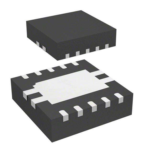
| 描述 | IC CTLR STEP-UP FOR LED 10-DFN显示驱动器和控制器 LED driver 0.8V-3.6V CNTRL FET N-CH PWM |
| 产品分类 | |
| 品牌 | STMicroelectronics |
| 产品手册 | |
| 产品图片 |
|
| rohs | 符合RoHS无铅 / 符合限制有害物质指令(RoHS)规范要求 |
| 产品系列 | 驱动器IC,显示驱动器和控制器,STMicroelectronics STLDC08PUR- |
| 数据手册 | |
| 产品型号 | STLDC08PUR |
| 产品 | LED Drivers |
| 产品种类 | 显示驱动器和控制器 |
| 供应商器件封装 | 10-DFN(3x3) |
| 其它名称 | 497-11140-6 |
| 其它有关文件 | http://www.st.com/web/catalog/sense_power/FM142/CL1974/SC1792/PF251671?referrer=70071840 |
| 内部驱动器 | 无 |
| 包装 | Digi-Reel® |
| 商标 | STMicroelectronics |
| 安装类型 | 表面贴装 |
| 安装风格 | SMD/SMT |
| 封装 | Reel |
| 封装/外壳 | 10-VFDFN 裸露焊盘 |
| 封装/箱体 | DFN-10 |
| 工作温度 | -40°C ~ 85°C |
| 工厂包装数量 | 3000 |
| 恒压 | - |
| 恒流 | - |
| 拓扑 | PWM,升压(升压) |
| 最大工作温度 | + 85 C |
| 最大输出电流 | 100 uA |
| 最小工作温度 | - 40 C |
| 标准包装 | 1 |
| 特色产品 | http://www.digikey.com/cn/zh/ph/st/stldc08.html |
| 电压-电源 | 0.8 V ~ 3.6 V |
| 电压-输出 | - |
| 电源电压 | 0.8 V to 3.6 V |
| 电源电流 | 3 mA |
| 类型-初级 | 通用 |
| 类型-次级 | - |
| 系列 | STLDC08 |
| 输出数 | 1 |
| 频率 | - |


- 商务部:美国ITC正式对集成电路等产品启动337调查
- 曝三星4nm工艺存在良率问题 高通将骁龙8 Gen1或转产台积电
- 太阳诱电将投资9.5亿元在常州建新厂生产MLCC 预计2023年完工
- 英特尔发布欧洲新工厂建设计划 深化IDM 2.0 战略
- 台积电先进制程称霸业界 有大客户加持明年业绩稳了
- 达到5530亿美元!SIA预计今年全球半导体销售额将创下新高
- 英特尔拟将自动驾驶子公司Mobileye上市 估值或超500亿美元
- 三星加码芯片和SET,合并消费电子和移动部门,撤换高东真等 CEO
- 三星电子宣布重大人事变动 还合并消费电子和移动部门
- 海关总署:前11个月进口集成电路产品价值2.52万亿元 增长14.8%


PDF Datasheet 数据手册内容提取
STLDC08 Step-up controller for LED supply Features ■ Input voltage range from 0.8 V to 3.6 V ■ Overvoltage protection ■ Drives N-channel MOSFET or NPN bipolar transistor ■ No control loop compensation required ■ FET driver for very precise PWM dimming DFN10 (3 x 3 mm) Applications ■ Single/dual cell NiMH, NiCd, or alkaline batteries ■ Small appliances LED lighting ■ Portable lighting Description The STLDC08 LED driver step-up controller is optimized to operate from one or two NiCd/NiMH or alkaline cells. The IC is able to drive an external MOSFET (N-channel) enabling it for use with wide power levels. Hysteretic control eliminates the need for small signal control loop compensation. The IC integrates an FET driver for a precise PWM dimming. STLDC08 comes in a DFN10 (3 x 3 mm) package. Table 1. Device summary Order code Marking Package STLDC08PUR STLDC08 DFN10 (3 x 3 mm.) February 2011 Doc ID 18476 Rev 1 1/29 www.st.com 29
Contents STLDC08 Contents 1 Application diagram . . . . . . . . . . . . . . . . . . . . . . . . . . . . . . . . . . . . . . . . . 3 2 Absolute maximum ratings . . . . . . . . . . . . . . . . . . . . . . . . . . . . . . . . . . . 5 3 Pin configuration . . . . . . . . . . . . . . . . . . . . . . . . . . . . . . . . . . . . . . . . . . . 6 4 Electrical characteristics . . . . . . . . . . . . . . . . . . . . . . . . . . . . . . . . . . . . . 7 5 Typical performance characteristics . . . . . . . . . . . . . . . . . . . . . . . . . . . . 9 6 Block diagram . . . . . . . . . . . . . . . . . . . . . . . . . . . . . . . . . . . . . . . . . . . . . 11 7 Detailed description . . . . . . . . . . . . . . . . . . . . . . . . . . . . . . . . . . . . . . . . 12 7.1 Main control loop . . . . . . . . . . . . . . . . . . . . . . . . . . . . . . . . . . . . . . . . . . . 12 7.2 Start up . . . . . . . . . . . . . . . . . . . . . . . . . . . . . . . . . . . . . . . . . . . . . . . . . . . 12 7.3 Over voltage protection (OVP) . . . . . . . . . . . . . . . . . . . . . . . . . . . . . . . . . 13 7.4 Enable/PWM . . . . . . . . . . . . . . . . . . . . . . . . . . . . . . . . . . . . . . . . . . . . . . 13 7.5 Dimming . . . . . . . . . . . . . . . . . . . . . . . . . . . . . . . . . . . . . . . . . . . . . . . . . . 14 8 Application information . . . . . . . . . . . . . . . . . . . . . . . . . . . . . . . . . . . . . 15 8.1 LED current programming . . . . . . . . . . . . . . . . . . . . . . . . . . . . . . . . . . . . 15 8.2 Duty cycle . . . . . . . . . . . . . . . . . . . . . . . . . . . . . . . . . . . . . . . . . . . . . . . . . 15 8.3 Inductor selection . . . . . . . . . . . . . . . . . . . . . . . . . . . . . . . . . . . . . . . . . . . 15 8.4 Inductor peak current limit . . . . . . . . . . . . . . . . . . . . . . . . . . . . . . . . . . . . 17 8.5 Power MOSFET selection . . . . . . . . . . . . . . . . . . . . . . . . . . . . . . . . . . . . 18 8.6 Schottky diode selection . . . . . . . . . . . . . . . . . . . . . . . . . . . . . . . . . . . . . . 20 8.7 Input capacitor . . . . . . . . . . . . . . . . . . . . . . . . . . . . . . . . . . . . . . . . . . . . . 20 8.8 Output capacitor . . . . . . . . . . . . . . . . . . . . . . . . . . . . . . . . . . . . . . . . . . . . 20 9 Demonstration board . . . . . . . . . . . . . . . . . . . . . . . . . . . . . . . . . . . . . . . 21 10 Layout suggestion . . . . . . . . . . . . . . . . . . . . . . . . . . . . . . . . . . . . . . . . . 22 11 Package mechanical data . . . . . . . . . . . . . . . . . . . . . . . . . . . . . . . . . . . . 24 2/29 Doc ID 18476 Rev 1
STLDC08 Contents 12 Revision history . . . . . . . . . . . . . . . . . . . . . . . . . . . . . . . . . . . . . . . . . . . 28 Doc ID 18476 Rev 1 3/29
Application diagram STLDC08 1 Application diagram Figure 1. Electric schematic optimized for 2 LEDs and I = 200 mA LED L1 D1 RF BATTERY C1 C2 D3 M1 C3 Rs D2 U1 4 9 VCC DRV EN/PWM 7 EN/PWM SENSE 6 C6 1 3 VOUT 2VCC 2 M2 C4 PWMOUT 10 5 V5 FB GND EXP C5 8 11 Rfb AM07845v1 Table 2. List of components Reference Manufacturer Part number Value Size C1 Murata GRM21BR60J475 4.7 µF, 6.3 V 0805 C2 Murata GRM31CB31C106K 10 µF, 16 V 1206 C4 Murata GRM188R70J103KA01B 10 nF, 6.3 V 0603 C3, C5, C6 Murata GRM188R61C105K 1 µF, 16 V 0603 L Coilcraft LPS6235-103ML 10 µH 6 mm x 6 mm M1,M2 STMicroelectronics STS5DNF20V SO-8 D1 STMicroelectronics STPS2L30 SMA Rfb 0.47 Ω 0805 Rs 0.047 Ω 0805 RF 0 Ω 0603 4/29 Doc ID 18476 Rev 1
STLDC08 Application diagram Figure 2. Electric schematic optimized for 4 LEDs and I = 300 mA LED L1 D1 RF BATTERY C1 C2 D4 D5 M1 C3 Rs D2 D3 U1 4 9 VCC DRV EN/PWM 7 EN/PWM SENSE 6 C6 1 3 VOUT 2VCC 2 M2 C4 PWMOUT 10 5 V5 FB GND EXP C5 8 11 Rfb AM07892v1 Table 3. List of components Part reference Manufacturer Part number Value Size C1 Murata GRM21BR60J106KE19 10 µF, 6.3 V 0805 C2 Murata GRM31CR61C226K 22 µF, 16 V 1206 C4 Murata GRM188R70J103KA01B 10 nF, 6.3 V 0603 C3, C5, C6 Murata GRM188R61C105K 1 µF, 16 V 0603 M1,M2 STMicroelectronics STS5DNF20V SO-8 D1 STMicroelectronics STPS2L30 SMA L Coilcraft DO3316P-223_L 22 µH 12.95 mm x 9.4 mm Rfb 0.33 Ω 0805 Rs 0.033 Ω 0805 RF 0 Ω 0603 Doc ID 18476 Rev 1 5/29
Absolute maximum ratings STLDC08 2 Absolute maximum ratings Table 4. Absolute maximum ratings Symbol Parameter Value Unit V Supply voltage - 0.3 to 4.6 V CC EN/PWM Analog input - 0.3 to 7 V FB Analog input - 0.3 to 2 V SENSE Analog input - 0.3 to 20 V 2V Analog outputs 0 to 4 V CC V5 Analog outputs - 0.3 to 7 V DRV, PWMOUT Analog outputs V - 1.2 to 7 V CC V Output voltage - 0.3 to 20 V OUT ESD Human body model (all pins) ±2 kV P DFN10L 3x3 T = 25 °C 2.2 W D A T Junction temperature - 40 to 85 °C J T Storage temperature range - 55 to 85 °C STG Note: Absolute maximum ratings are those values beyond which damage to the device may occur. Functional operation under these conditions is not implied. Table 5. Thermal data Symbol Parameter Value Unit R Thermal resistance junction-case 3 °C/W thJC R Thermal resistance junction-ambient 57.1 (1) °C/W thJA 1. With two sides, two planes PCB following EIA/JEDEC JESD51-7 standard. 6/29 Doc ID 18476 Rev 1
STLDC08 Pin configuration 3 Pin configuration Figure 3. Pin connections (top through view) Bottom view Top view Table 6. Pin description Pin # Pin name Pin function 1 VOUT Over voltage protection and supply pin for the IC when V > 2 V OUT Driver of the external MOSFET for PWM dimming. The driver stage is controlled by 2 PWMOUT EN/PWM signal 3 2Vcc Charge pump output Supply voltage when V < 2 V, this pin represents the input of the internal charge 4 VCC OUT pump 5 FB Feedback pin for LED current control 6 SENSE Sense resistor for current mode control and peak current limit 7 EN/PWM Enable pin and PWM control input for PWMOUT pin 8 GND Ground reference 9 DRV Driver output for Boost stage MOSFET Internal regulator output. Decouple this pin locally to the IC ground with a minimum 10 V5 of 1 µF ceramic capacitor Exposed Pad The exposed pad needs to be connected and soldered to analog ground Doc ID 18476 Rev 1 7/29
Electrical characteristics STLDC08 4 Electrical characteristics T = -40 to 85; C = 22 µF; C =10 µF; PWMOUT = 3300 pF; DVR = 3300 pF; 2V =10 A IN OUT CC nF; V5 =1 µF; V = 1.5V; V = 3 V; FB = GND; SENSE = GND; EN/PWM = V ; unless CC OUT CC otherwise specified. Table 7. Electrical characteristics Symbol Parameter Test conditions Min. Typ. Max. Unit General section V Supply voltage range V = GND 0.8 3.6 V CC OUT Supply current measured on V CC V = GND 3 mA I pin with charge pump ON OUT VCC Shutdown current EN = GND Shutdown mode 5 10 µA OVP Overvoltage protection Rising edge 18 19.5 V V = 3 V, FB = 500 mV (no OUT 60 100 µA switching) Operating supply current V = 3 V, FB = GND OUT 800 µA IVOUT measured on VOUT pin (switching) V = 10 V, FB = GND OUT 1.3 2 mA (switching) Shutdown current EN = GND 5 10 µA 2VCC Charge pump ON V floating; V = 0.8 V 1.5 V OUT CC Driver section (DRV output) V Low level voltage I = 100 mA 80 160 mV DRVL DRV V High level voltage I = -100 mA 120 240 mV DRVH DRV t Rise time C = 3300 pF 30 ns R DRV t Fall time C = 3300 pF 20 ns F DRV FB V Feedback voltage T = 25 °C 90 105 116 mV FB A I Bias current FB = 2 V 20 500 nA FB Timing T Minimum Off time 1 µs OFF(MIN) T Maximum On time 20 µs ON(MAX) PWM OUT section V Low level voltage I = 100 mA 200 400 mV PWMOUTL PWMOUT V High level voltage I = - 100 mA 250 500 mV PWMOUTH PWMOUT t Rise time C = 3300 pF 30 ns r PWMOUT t Fall time C = 3300 pF 20 ns f PWMOUT 8/29 Doc ID 18476 Rev 1
STLDC08 Electrical characteristics Table 7. Electrical characteristics (continued) Symbol Parameter Test conditions Min. Typ. Max. Unit SENSE Maximum current sense V 70 100 130 mV SENSE MAX threshold I Bias current V = 20 V 10 20 µA SENSE SENSE EN/PWM section V Low level threshold V = 0.8 V 0.3 V IL CC V Low level threshold V = 3.6 V 0.4 V IL CC V High level threshold V = 0.8 V 0.8 V IH CC V High level threshold V = 3.6 V 1.2 V IH CC I EN/PWM pin current EN/PWM = 3.6 V 2 µA EN/PWM I EN/PWM pin current EN/PWM = 5 V 5 µA EN/PWM + 5 V regulator V5 Output voltage V = 6 V; I5 = 10 mA 4.8 5 5.2 V OUT ΔV5/ΔV Line regulation 6 V < V < 18 V; I5 = 10 mA 0.02 %/V OUT OUT ΔV5 Load regulation 0 < I5 < 10 mA V = 18 V 0.02 0.01 %/mA OUT V Dropout voltage I5 = 10 mA 20 mV DROPOUT I Short circuit current V = 18 V; V5 = 0 V 140 mA CC OUT Doc ID 18476 Rev 1 9/29
Typical performance characteristics STLDC08 5 Typical performance characteristics Figure 4. V vs. temperature Figure 5. Maximum V vs. temperature FB SENSE (cid:33)(cid:45)(cid:16)(cid:23)(cid:24)(cid:25)(cid:19)(cid:86)(cid:17) (cid:33)(cid:45)(cid:16)(cid:23)(cid:24)(cid:25)(cid:20)(cid:86)(cid:17) (cid:17)(cid:16)(cid:18) (cid:17)(cid:22)(cid:16) (cid:17)(cid:20)(cid:16) (cid:17)(cid:16)(cid:17) (cid:17)(cid:18)(cid:16) (cid:17)(cid:16)(cid:16) (cid:54)(cid:61)(cid:17)(cid:16)(cid:16) (cid:54)(cid:61) (cid:77) (cid:54)(cid:59)(cid:77)(cid:38)(cid:34) (cid:25)(cid:25)(cid:24)(cid:25) (cid:54)(cid:59)(cid:51)(cid:37)(cid:46)(cid:51)(cid:37) (cid:22)(cid:24)(cid:16)(cid:16) (cid:20)(cid:16) (cid:25)(cid:23) (cid:54)(cid:47)(cid:53)(cid:52)(cid:29)(cid:0)(cid:19)(cid:14)(cid:20)(cid:0)(cid:54) (cid:18)(cid:16) (cid:54)(cid:47)(cid:53)(cid:52)(cid:29)(cid:0)(cid:19)(cid:14)(cid:20)(cid:0)(cid:54) (cid:25)(cid:22) (cid:16) (cid:13)(cid:21)(cid:16) (cid:13)(cid:18)(cid:21) (cid:16) (cid:18)(cid:21) (cid:21)(cid:16) (cid:23)(cid:21) (cid:17)(cid:16)(cid:16) (cid:17)(cid:18)(cid:21) (cid:17)(cid:21)(cid:16) (cid:13)(cid:21)(cid:16) (cid:13)(cid:18)(cid:21) (cid:16) (cid:18)(cid:21) (cid:21)(cid:16) (cid:23)(cid:21) (cid:17)(cid:16)(cid:16) (cid:17)(cid:18)(cid:21) (cid:17)(cid:21)(cid:16) (cid:52)(cid:69)(cid:77)(cid:80)(cid:69)(cid:82)(cid:65)(cid:84)(cid:85)(cid:82)(cid:69)(cid:59)(cid:160)(cid:35)(cid:61) (cid:52)(cid:69)(cid:77)(cid:80)(cid:69)(cid:82)(cid:65)(cid:84)(cid:85)(cid:82)(cid:69)(cid:0)(cid:59)(cid:160)(cid:35)(cid:61) Figure 6. I vs. temperature FB = 0.5 V Figure 7. I vs. temperature FB = GND OUT OUT (cid:33)(cid:45)(cid:16)(cid:23)(cid:24)(cid:25)(cid:21)(cid:86)(cid:17) (cid:33)(cid:45)(cid:16)(cid:23)(cid:24)(cid:25)(cid:22)(cid:86)(cid:17) (cid:17)(cid:16)(cid:16) (cid:17)(cid:14)(cid:20) (cid:25)(cid:21) (cid:17)(cid:14)(cid:18) (cid:25)(cid:16) (cid:24)(cid:21) (cid:17) (cid:151)(cid:33)(cid:61) (cid:24)(cid:16) (cid:77)(cid:33)(cid:61) (cid:16)(cid:14)(cid:24) (cid:41)(cid:59)(cid:54)(cid:47)(cid:53)(cid:52)(cid:23)(cid:23)(cid:16)(cid:21) (cid:41)(cid:59)(cid:54)(cid:47)(cid:53)(cid:52) (cid:16)(cid:14)(cid:22) (cid:22)(cid:21) (cid:16)(cid:14)(cid:20) (cid:22)(cid:16) (cid:21)(cid:21) (cid:54)(cid:47)(cid:53)(cid:52)(cid:29)(cid:0)(cid:17)(cid:16)(cid:0)(cid:54)(cid:12)(cid:0)(cid:38)(cid:34)(cid:0)(cid:29)(cid:0)(cid:16)(cid:14)(cid:21)(cid:0)(cid:54) (cid:16)(cid:14)(cid:18) (cid:54)(cid:47)(cid:53)(cid:52)(cid:29)(cid:0)(cid:17)(cid:16)(cid:0)(cid:54)(cid:12)(cid:0)(cid:38)(cid:34)(cid:0)(cid:29)(cid:0)(cid:39)(cid:46)(cid:36) (cid:21)(cid:16) (cid:16) (cid:13)(cid:21)(cid:16) (cid:13)(cid:18)(cid:21) (cid:16) (cid:18)(cid:21) (cid:21)(cid:16) (cid:23)(cid:21) (cid:17)(cid:16)(cid:16) (cid:17)(cid:18)(cid:21) (cid:17)(cid:21)(cid:16) (cid:13)(cid:21)(cid:16) (cid:13)(cid:18)(cid:21) (cid:16) (cid:18)(cid:21) (cid:21)(cid:16) (cid:23)(cid:21) (cid:17)(cid:16)(cid:16) (cid:17)(cid:18)(cid:21) (cid:17)(cid:21)(cid:16) (cid:52)(cid:69)(cid:77)(cid:80)(cid:69)(cid:82)(cid:65)(cid:84)(cid:85)(cid:82)(cid:69)(cid:0)(cid:59)(cid:160)(cid:35)(cid:61) (cid:52)(cid:69)(cid:77)(cid:80)(cid:69)(cid:82)(cid:65)(cid:84)(cid:85)(cid:82)(cid:69)(cid:0)(cid:59)(cid:160)(cid:35)(cid:61) Figure 8. Efficiency vs. input voltage 2 LEDs Figure 9. Efficiency vs. input voltage 4 LEDs (cid:33)(cid:45)(cid:16)(cid:23)(cid:24)(cid:25)(cid:23)(cid:86)(cid:17) (cid:33)(cid:45)(cid:16)(cid:23)(cid:24)(cid:25)(cid:24)(cid:86)(cid:17) (cid:17)(cid:16)(cid:16) (cid:17)(cid:16)(cid:16) (cid:25)(cid:21) (cid:25)(cid:21) (cid:25)(cid:16) (cid:25)(cid:16) (cid:24)(cid:21) (cid:24)(cid:21) (cid:24)(cid:16) (cid:24)(cid:16) (cid:5)(cid:61) (cid:23)(cid:21) (cid:5)(cid:61) (cid:23)(cid:21) (cid:59) (cid:59) (cid:37)(cid:70)(cid:70) (cid:23)(cid:16) (cid:37)(cid:70)(cid:70) (cid:23)(cid:16) (cid:22)(cid:21) (cid:22)(cid:21) (cid:22)(cid:16) (cid:22)(cid:16) (cid:21)(cid:21) (cid:41)(cid:44)(cid:37)(cid:36)(cid:29)(cid:0)(cid:18)(cid:16)(cid:16)(cid:0)(cid:77)(cid:33)(cid:12)(cid:0)(cid:18)(cid:0)(cid:44)(cid:37)(cid:36)(cid:83) (cid:21)(cid:21) (cid:41)(cid:44)(cid:37)(cid:36)(cid:29)(cid:0)(cid:19)(cid:16)(cid:16)(cid:0)(cid:77)(cid:33)(cid:12)(cid:0)(cid:20)(cid:0)(cid:44)(cid:37)(cid:36)(cid:83) (cid:21)(cid:16) (cid:21)(cid:16) (cid:16)(cid:14)(cid:24) (cid:17)(cid:14)(cid:18) (cid:17)(cid:14)(cid:22) (cid:18) (cid:18)(cid:14)(cid:20) (cid:18)(cid:14)(cid:24) (cid:19)(cid:14)(cid:18) (cid:19)(cid:14)(cid:22) (cid:17)(cid:14)(cid:22) (cid:17)(cid:14)(cid:24) (cid:18) (cid:18)(cid:14)(cid:18) (cid:18)(cid:14)(cid:20) (cid:18)(cid:14)(cid:22) (cid:18)(cid:14)(cid:24) (cid:19) (cid:19)(cid:14)(cid:18) (cid:19)(cid:14)(cid:20) (cid:19)(cid:14)(cid:22) (cid:54)(cid:35)(cid:35)(cid:59)(cid:54)(cid:61) (cid:54)(cid:35)(cid:35)(cid:59)(cid:54)(cid:61) 10/29 Doc ID 18476 Rev 1
STLDC08 Typical performance characteristics Figure 10. Startup timing and dimming I Figure 11. Dimming EN/PWM = 200 Hz, 2 LEDs LED vs. time, 2 LEDs VCC = 1.5 V; ILED = 200 mA 2LEDs VCC = 1.5 V; ILED = 200 mA 2LEDs Figure 12. Startup timing and dimming I Figure 13. Dimming EN/PWM = 200 Hz, 4 LEDs LED vs. time, 4 LEDs VCC = 3.6 V; ILED = 300 mA 4LEDs VCC = 3.6 V; ILED = 300 mA 4LEDs Figure 14. V = 1.5 V; I = 200 mA, 2LEDs Figure 15. V = 3.6 V; I = 300 mA, 4LEDs CC LED CC LED Doc ID 18476 Rev 1 11/29
Block diagram STLDC08 6 Block diagram Figure 16. Block diagram VVOOUUTT VVcccc OOvveerr VVoollttaaggee VVOOUUTT ++ PPrrootteeccttiioonn -- OOVVPP TTHH ++55 VV LLDDOO CChhaarrggee 22VVcccc ++55 VV PPuummpp 22VVcccc TTOOFFFF ttiimmeerr TT == 11 µµsseecc SS OOFFFF DDRRVV QQ DDRRIIVVEERR RR GGGGNNNNDDDD TTOONNMMAAXX == 2200 µµsseecc PPeeaakk CCuurrrreenntt CCoommppaarraattoorr SSEENNSSEE ++ OOCCPP SSeennsseedd OOCCPP__TTHH CCuurrrreenntt RRaammpp RREESSEETT -- OOCCPP__TTHH PPeeaakk CCuurrrreenntt -- FFBB CCoonnttrrooll FFBB ++ 110000 mmVV FFeeeeddbbaacckk CCoommppaarraattoorr EENN//PPWWMM PPWWMMOOUUTT DDRRIIVVEERR AAMM0077884466vv11 12/29 Doc ID 18476 Rev 1
STLDC08 Detailed description 7 Detailed description 7.1 Main control loop The STLDC08 is an LED driver step-up controller dedicated to handheld equipment, having a typical voltage ranging from 0.8 V to 1.5 V. The controller drives an N-channel Power MOSFET and implements a hysteretic current mode control with constant OFF time. Hysteretic operation eliminates the need for small signal control loop compensation. The control loop adapts the value of the inductor peak current as needed to deliver the desired current on the LED branch. The LED current is set by an external sense resistor R FB inserted between the feedback pin (FB) and GND. When the current mode control system operates in continuous mode the control peak current is almost equivalent to the average current control. 7.2 Start up At the startup phase, when the device is connected to the battery or when the EN pin is pulled high, the internal 2x charge pump starts to work, boosting the voltage on the 2V CC pin. When the 2V pin reaches 1.7 V a soft-start cycle begins. The external main MOSFET CC is switched on/off allowing the charging of the output capacitor. If the optional PWMOUT MOSFET is used for the dimming operation, the PWMOUT pin is held low, further assuring that no current is flowing. The PWMOUT pin starts to follow the PWM input when the soft-start cycle is ended. When V voltage exceeds 1.9 V, the chip starts drawing its supply current from V OUT OUT rather than from V , the charge pump is turned off and the voltage on the 2V pin goes to CC CC zero. When V exceeds the forward voltage of LED V , the current starts flowing trough OUT LED the LED, but, at this point, the voltage on the DRV pin is high enough to allow the main MOSFET to carry the necessary current. Doc ID 18476 Rev 1 13/29
Detailed description STLDC08 Figure 17. Timing diagram VV CCCC 11..77 VV 22VVCCCC 11..99 VV VV OOUUTT DDRRVV VV >>11..99 VV SSTTLLDDCC0088 iiss OOUUTT II ssuupppplliieedd bbyy VV CCCC OOUUTT VV >> VV ,, tthhee ccuurrrreenntt ssttaarrttss OOUUTT LLEEDD fflloowwiinngg tthhrroouugghh tthhee LLEEDDss IILLEEDD FFoolllloowwss EENN//PPWWMM iinnppuutt SSoofftt ssttaarrtt ccyyccllee eennddeedd,, PPWWMMOOUUTT iiss rreeaalleeaasseedd PPWWMMOOUUTT CChhaarrggee PPuummpp SSTTLLDDCC0088 ssuupppplliieedd bbyy aaccttiivvee VV OOUUTT AAMM0077884477vv11 7.3 Over voltage protection (OVP) As with any current source, the output voltage rises when the output gets high impedance or is disconnected. To prevent the output voltage exceeding the maximum switch voltage rating of the main switch, an overvoltage protection circuit is integrated. As soon as the output voltage exceeds the OVP threshold, the converter stops switching and the output voltage drops. When the output voltage falls below the OVP threshold, the converter continues operation until the output voltage exceeds the OVP threshold again. 7.4 Enable/PWM The enable pin allows disabling and enabling of the device as well as brightness control of the LEDs by applying a PWM signal. In order to avoid visible flicker, the frequency of the PWM signal should be higher than 120 Hz. Changing the PWM duty cycle therefore changes the LED brightness. 14/29 Doc ID 18476 Rev 1
STLDC08 Detailed description 7.5 Dimming When PWMOUT goes to zero, the LED current immediately goes to zero and the energy stored in the coil is discharged on the output capacitor, causing an increase in the output voltage. As soon as the PWM goes back to high value, there is a big spike current on the LED. This could damage the LED itself. To avoid this, as soon as the input PWM signal goes to zero the controller immediately turns off the main switch (in order to discharge the coil current on the LED branch). In this way the PWM power is turned off with a delay in order to guarantee that FB goes high after PowerMOS turn off. After this delay, the flip-flop is ready to be set and the PWM power is turned off. In this condition the output voltage is slightly lower than the regulated value, but a current spike on the LED is avoided. Doc ID 18476 Rev 1 15/29
Application information STLDC08 8 Application information 8.1 LED current programming The LED current is set by an external resistor connected between the FB pin and GND. The following equation can be used to calculate the value of the R resistor which guarantees FB the desired output current: Equation 1 0.1 RFB= ILED The feedback signal V is compared with the internal precision 100 mV voltage reference FB by the error amplifier. The internal reference has a guaranteed tolerance of 10 %. Tolerance of the sense resistor adds additional error to the output voltage. 1 % resistors are recommended. 8.2 Duty cycle The controlled off-time architecture is a hysteretic mode control. Hysteretic operation eliminates the need for small signal control loop compensation. When the converter runs in continuous conduction mode (CCM) the controller adapts the T time in order to obtain the ON duty cycle given by the following relationship: Equation 2 D=1− VIN VOUT+VD where V is the output voltage given by: O Equation 3 VO=n×VF(LED)+VFB and VD is the forward voltage of the Schottky diode. 8.3 Inductor selection As the hysteretic control scheme is inherently stable, the inductor value does not affect the stability of the regulator. The switching frequency, peak inductor current, and allowable ripple of the output current determine the value of the inductor. LED manufacturers generally recommend a value for LED current ripple ranging from 5 % to 20 % of LED average current. 16/29 Doc ID 18476 Rev 1
STLDC08 Application information As a first approximation we choose the inductor ripple current, I , equal to approximately 40 L % of the output current. Higher ripple current allows for smaller inductors, but it also increases the output capacitance for a given LED current ripple requirement. Conversely, lower ripple current can be obtained increasing the value of the inductance, and this enables a reduction of the output capacitor value. This trade-off can be altered once standard inductance and capacitance values are chosen. I is determined by the input and output voltage, the value of the inductance, and T . L OFF Figure 18. Timing diagram II PPEEAAKK II LL II RRIIPPPPLLEE II II == OOUUTT IINN II 11−−DD OOUUTT tt TT TT OONN OOFFFF AAMM0077884488vv11 The minimum value of inductance which guarantees the fixed inductor ripple current can be determined using the following equation: Equation 4 L>(VOUT+Vd-VINMIN)×TOFF (ΔIL) where V is the forward drop of the Schottky diode, I is the fixed inductor ripple current, and d L T is the constant OFF time. OFF The following equation shows the average inductor current as a function of the output current and duty cycle. Equation 5 IL(AVG)=ILED 1−D An inductor that can carry the maximum input DC current which occurs at the minimum input voltage should be chosen. The peak-to-peak ripple current is set by the inductance and a good starting point is to choose a ripple current of at least 40 % of its maximum value of the: Doc ID 18476 Rev 1 17/29
Application information STLDC08 Equation 6 ΔIL =40%×IL(AVG)=40%× ILED 1−DMAX Where D is given by: MAX Equation 7 VIN(MIN) DMAX =1− VOUT+VD The value of the peak current on the inductor is given by the following equation: Equation 8 IL(PK)=IL(AVG)+ΔIL 2 The minimum required saturation current of the inductor must be greater than I and can L(PK) be expressed as follows: Equation 9 IL(SAT)>IL(PK)= IOUT +ΔIL 1−DMAX 2 The saturation current rating for the inductor should be checked at the maximum duty cycle and maximum output current. 8.4 Inductor peak current limit The value of the inductor peak current limit can be programmed either by using a sense resistor or by using the RDSON of the main Power MOSFET. The following equation gives the relationship between the peak current limit and the value of the sense resistor: Equation 10 IIN(MAX)= VSENSE = 0.1 RSENSE RSENSE The sense resistor value can be determined fixing the value of the inductor peak current limit equal to twice the value of the inductor peak current in steady-state conditions. 18/29 Doc ID 18476 Rev 1
STLDC08 Application information Equation 11 IIN(MAX)=2×IL(PK) Equation 12 IL(PK)= ILED +ΔIL 1−DMAX 2 Equation 13 0.1 RSENSE= 2×IL(PK) If the R of the main Power MOSFET is used to sense the current on the inductor the DS (ON) following procedure must be performed to choose the Power MOSFET. During ON time, the SENSE comparator limits the voltage across the Power MOSFET to a nominal 100 mV. In that case, the maximum inductor current is given by the following relationships: Equation 14 IL(MAX)= VSENSE = 100mV RDS(ON) RDS(ON) Equation 15 IL(MAX)=2×IL(PK)=2× ILED ×⎜⎜⎛1+ΔIL⎟⎟⎞ 1−DMAX ⎝ 2 ⎠ Equation 16 RDS(ON)<0.1× 1−DMAX 2×ILED×⎜⎛1+ΔIL⎟⎞ ⎝ 2 ⎠ 8.5 Power MOSFET selection A key parameter to take into account in the selection of the N-MOSFET is the maximum continuous drain current. As a safety design, it is important to choose a maximum continuous drain current equal to twice the maximum input current. Doc ID 18476 Rev 1 19/29
Application information STLDC08 Figure 19. Current diagram ON state LL11 LLXX DD11 VVBBAATT CCIINN CCOOUUTT DDVVRR LLEEDD SSEENNSSEE RRsseennssee SSTTLLDDCC0088 VVOOUUTT FFBB OONN ssttaattee RR FFBB AAMM0077884499vv11 Figure 20. Current diagram OFF state LL11 LLXX DD11 VVBBAATT CC IINN CC OOUUTT DDVVRR LLEEDD SSEENNSSEE RRsseennssee SSTTLLDDCC0088 VVOOUUTT FFBB OOFFFF ssttaattee RR FFBB AAMM0077885500vv11 Another important parameter is the drain source breakdown voltage. During the ON state, the potential of the LX point is 0 V, while during the OFF state the potential of this point rises to the output voltage plus the forward voltage of the D1. Therefore, the absolute V rating DS of the main switch must be greater than this voltage to prevent main switch damage. 20/29 Doc ID 18476 Rev 1
STLDC08 Application information 8.6 Schottky diode selection Schottky diodes, with their low forward voltage and fast recovery time, are the ideal choice to maximize efficiency. The output diode in a boost converter conducts current only when the power switch is OFF. The average current is equal to the output current and the peak current is equal to the peak inductor current. Ensure that the diode's average and peak current ratings exceed the average and peak inductor current, respectively. In addition, the diode's reverse breakdown voltage must exceed the regulator output voltage. 8.7 Input capacitor The input capacitor of a boost converter is less critical than the output capacitor, due to the fact that the input current waveform is continuous. The input voltage source impedance determines the size of the input capacitor, which is typically in the range of 10 µF to 100 µF. A low ESR capacitor is recommended though it is not as critical as the output capacitor. 8.8 Output capacitor For best output voltage filtering, a low ESR output capacitor is recommended. Ceramic capacitors have a low ESR value but tantalum capacitors can be used as well, depending on the application. The output voltage ripple consists of two parts, the first is the product I ESR, the second L(PK) is caused by the charging and discharging process of the output capacitor. Equation 17 ΔVOUT = TON×ILED +ESR×IL(PK) COUT where: I = Peak current L(PK) I = Load current LED C = Selected output capacitor OUT ESR = Output capacitor ESR value Doc ID 18476 Rev 1 21/29
Demonstration board STLDC08 9 Demonstration board Figure 21. Electrical schematic TP1 TP2 TP3 VIN SW VOUT J1 1 L1 1 D1 1 J3 1 1 2 2 RF TP5 POWER IN C1 C2 LED 1 J2 TP4 M1 1 C3 DRV 1 2 SENSE GND Rs U1 J4 4 9 1 VCC DRV 2 7 6 3 EN/PWM SENSE C6 1 3 VOUT EN/PWM 2VCC 2 M2 C4 PWMOUT 10 5 V5 FB GND EXP C5 8 11 Rfb AM07900v1 Table 8. Bill of material optimized for 2 LEDs and I = 200 mA LED Reference Manufacturer Part number Value Size C1 Murata GRM21BR60J475 4.7 µF 6.3V 0805 C2 Murata GRM31CB31C106K 10 µF 16 V 1206 C4 Murata GRM188R70J103KA01B 10 nF, 6.3 V 0603 C3, C5, C6 Murata GRM188R61C105K 1 µF, 16 V 0603 L Coilcraft LPS6235-103ML 10µH 6 mm x 6 mm M1,M2 STMicroelectronics STS5DNF20V SO-8 D1 STMicroelectronics STPS2L30 SMA Rfb 0.47 Ω 0805 Rs 0.047 Ω 0805 RF 0 Ω 22/29 Doc ID 18476 Rev 1
STLDC08 Layout suggestion 10 Layout suggestion Figure 22. Assembly layer Figure 23. Top layer Doc ID 18476 Rev 1 23/29
Layout suggestion STLDC08 Figure 24. Bottom layer 24/29 Doc ID 18476 Rev 1
STLDC08 Package mechanical data 11 Package mechanical data In order to meet environmental requirements, ST offers these devices in different grades of ECOPACK® packages, depending on their level of environmental compliance. ECOPACK® specifications, grade definitions and product status are available at: www.st.com. ECOPACK® is an ST trademark. Doc ID 18476 Rev 1 25/29
Package mechanical data STLDC08 DFN10 (3x3 mm) mechanical data mm. mils. Dim. Min. Typ. Max. Min. Typ. Max. A 0.80 0.90 1.00 31.5 35.4 39.4 A1 0.02 0.05 0.8 2.0 A2 0.55 0.65 0.80 21.7 25.6 31.5 A3 0.20 7.9 b 0.18 0.25 0.30 7.1 9.8 11.8 D 2.85 3.00 3.15 112.2 118.1 124.0 D2 2.20 86.6 E 2.85 3.00 3.15 112.2 118.1 124.0 E2 1.40 1.75 55.1 68.9 e 0.50 19.7 L 0.30 0.40 0.50 11.8 15.7 19.7 ddd 0.08 3.1 7426335F 26/29 Doc ID 18476 Rev 1
STLDC08 Package mechanical data Tape & reel QFNxx/DFNxx (3x3) mechanical data mm. inch. Dim. Min. Typ. Max. Min. Typ. Max. A 180 7.087 C 12.8 13.2 0.504 0.519 D 20.2 0.795 N 60 2.362 T 14.4 0.567 Ao 3.3 0.130 Bo 3.3 0.130 Ko 1.1 0.043 Po 4 0.157 P 8 0.315 Doc ID 18476 Rev 1 27/29
Revision history STLDC08 12 Revision history Table 9. Document revision history Date Revision Changes 22-Feb-2011 1 First release. 28/29 Doc ID 18476 Rev 1
STLDC08 Please Read Carefully: Information in this document is provided solely in connection with ST products. STMicroelectronics NV and its subsidiaries (“ST”) reserve the right to make changes, corrections, modifications or improvements, to this document, and the products and services described herein at any time, without notice. All ST products are sold pursuant to ST’s terms and conditions of sale. Purchasers are solely responsible for the choice, selection and use of the ST products and services described herein, and ST assumes no liability whatsoever relating to the choice, selection or use of the ST products and services described herein. No license, express or implied, by estoppel or otherwise, to any intellectual property rights is granted under this document. If any part of this document refers to any third party products or services it shall not be deemed a license grant by ST for the use of such third party products or services, or any intellectual property contained therein or considered as a warranty covering the use in any manner whatsoever of such third party products or services or any intellectual property contained therein. UNLESS OTHERWISE SET FORTH IN ST’S TERMS AND CONDITIONS OF SALE ST DISCLAIMS ANY EXPRESS OR IMPLIED WARRANTY WITH RESPECT TO THE USE AND/OR SALE OF ST PRODUCTS INCLUDING WITHOUT LIMITATION IMPLIED WARRANTIES OF MERCHANTABILITY, FITNESS FOR A PARTICULAR PURPOSE (AND THEIR EQUIVALENTS UNDER THE LAWS OF ANY JURISDICTION), OR INFRINGEMENT OF ANY PATENT, COPYRIGHT OR OTHER INTELLECTUAL PROPERTY RIGHT. UNLESS EXPRESSLY APPROVED IN WRITING BY AN AUTHORIZED ST REPRESENTATIVE, ST PRODUCTS ARE NOT RECOMMENDED, AUTHORIZED OR WARRANTED FOR USE IN MILITARY, AIR CRAFT, SPACE, LIFE SAVING, OR LIFE SUSTAINING APPLICATIONS, NOR IN PRODUCTS OR SYSTEMS WHERE FAILURE OR MALFUNCTION MAY RESULT IN PERSONAL INJURY, DEATH, OR SEVERE PROPERTY OR ENVIRONMENTAL DAMAGE. ST PRODUCTS WHICH ARE NOT SPECIFIED AS "AUTOMOTIVE GRADE" MAY ONLY BE USED IN AUTOMOTIVE APPLICATIONS AT USER’S OWN RISK. Resale of ST products with provisions different from the statements and/or technical features set forth in this document shall immediately void any warranty granted by ST for the ST product or service described herein and shall not create or extend in any manner whatsoever, any liability of ST. ST and the ST logo are trademarks or registered trademarks of ST in various countries. Information in this document supersedes and replaces all information previously supplied. The ST logo is a registered trademark of STMicroelectronics. All other names are the property of their respective owners. © 2011 STMicroelectronics - All rights reserved STMicroelectronics group of companies Australia - Belgium - Brazil - Canada - China - Czech Republic - Finland - France - Germany - Hong Kong - India - Israel - Italy - Japan - Malaysia - Malta - Morocco - Philippines - Singapore - Spain - Sweden - Switzerland - United Kingdom - United States of America www.st.com Doc ID 18476 Rev 1 29/29
Mouser Electronics Authorized Distributor Click to View Pricing, Inventory, Delivery & Lifecycle Information: S TMicroelectronics: STLDC08PUR