ICGOO在线商城 > 集成电路(IC) > 接口 - 驱动器,接收器,收发器 > ST3222ECTR

 Datasheet下载
- 型号: ST3222ECTR
- 制造商: STMicroelectronics
- 库位|库存: xxxx|xxxx
- 要求:
| 数量阶梯 | 香港交货 | 国内含税 |
| +xxxx | $xxxx | ¥xxxx |
查看当月历史价格
查看今年历史价格
ST3222ECTR产品简介:
ICGOO电子元器件商城为您提供ST3222ECTR由STMicroelectronics设计生产,在icgoo商城现货销售,并且可以通过原厂、代理商等渠道进行代购。 ST3222ECTR价格参考。STMicroelectronicsST3222ECTR封装/规格:接口 - 驱动器,接收器,收发器, 2/2 Transceiver Full RS232 20-TSSOP。您可以下载ST3222ECTR参考资料、Datasheet数据手册功能说明书,资料中有ST3222ECTR 详细功能的应用电路图电压和使用方法及教程。
STMicroelectronics的ST3222ECTR是一款RS-232接口收发器,属于接口驱动器、接收器、收发器类别。该芯片主要用于实现TTL/CMOS电平与RS-232电平之间的双向转换,适用于需要串行通信的嵌入式系统和工业控制设备。

典型应用场景包括:工业自动化设备中的控制器与上位机通信、医疗仪器的数据传输模块、POS终端、测试测量仪器以及通信网关等。ST3222ECTR支持高达1Mbps的数据速率,具备低功耗特性,适合对功耗敏感的应用环境。其工作电压为3V至5.5V,兼容多种电源系统,增强了设计灵活性。

该器件采用小型化的TSSOP-16封装,节省PCB空间,适用于紧凑型电子产品设计。内置电荷泵仅需外接4个小型电容即可生成符合RS-232标准的正负电压信号(如±10V),简化了外围电路设计。同时,它具备良好的抗干扰能力和ESD保护功能,可在较宽的温度范围内稳定工作(-40°C 至 +85°C),适应工业级应用需求。

综上,ST3222ECTR广泛应用于需要可靠、高效串行通信的中低端嵌入式系统中,是传统RS-232接口升级或设计的理想选择之一。
| 参数 | 数值 |
| 产品目录 | 集成电路 (IC) |
| 描述 | IC DRVR/RCVR RS232 LPESD 20TSSOP |
| 产品分类 | |
| 品牌 | STMicroelectronics |
| 数据手册 | |
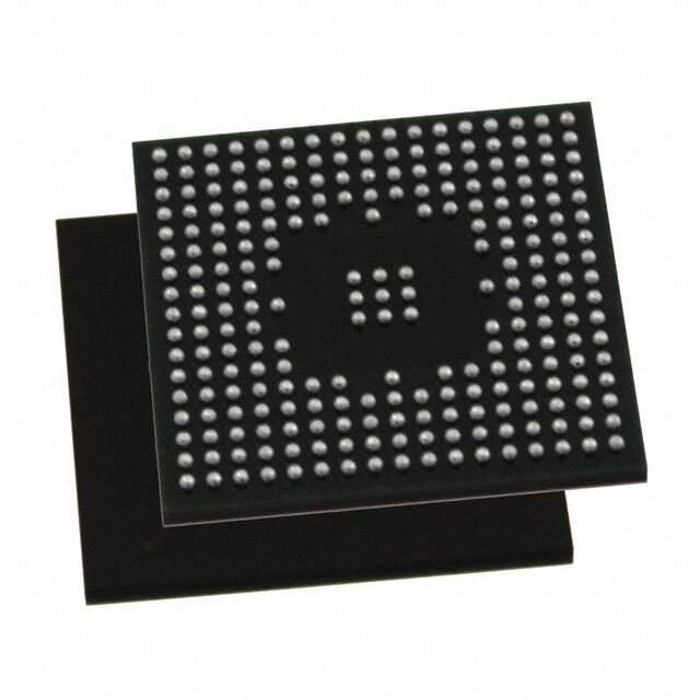
| 产品图片 |
|
| 产品型号 | ST3222ECTR |
| rohs | 无铅 / 符合限制有害物质指令(RoHS)规范要求 |
| 产品系列 | - |
| 产品目录页面 | |
| 供应商器件封装 | 20-TSSOP |
| 其它名称 | 497-7926-1 |
| 其它有关文件 | http://www.st.com/web/catalog/sense_power/FM1968/CL1179/SC392/PF66112?referrer=70071840 |
| 包装 | 剪切带 (CT) |
| 协议 | RS232 |
| 双工 | 全 |
| 安装类型 | 表面贴装 |
| 封装/外壳 | 20-TSSOP(0.173",4.40mm 宽) |
| 工作温度 | 0°C ~ 70°C |
| 接收器滞后 | 500mV |
| 数据速率 | 250kbps |
| 标准包装 | 1 |
| 电压-电源 | 3 V ~ 5.5 V |
| 类型 | 收发器 |
| 驱动器/接收器数 | 2/2 |


- 商务部:美国ITC正式对集成电路等产品启动337调查
- 曝三星4nm工艺存在良率问题 高通将骁龙8 Gen1或转产台积电
- 太阳诱电将投资9.5亿元在常州建新厂生产MLCC 预计2023年完工
- 英特尔发布欧洲新工厂建设计划 深化IDM 2.0 战略
- 台积电先进制程称霸业界 有大客户加持明年业绩稳了
- 达到5530亿美元!SIA预计今年全球半导体销售额将创下新高
- 英特尔拟将自动驾驶子公司Mobileye上市 估值或超500亿美元
- 三星加码芯片和SET,合并消费电子和移动部门,撤换高东真等 CEO
- 三星电子宣布重大人事变动 还合并消费电子和移动部门
- 海关总署:前11个月进口集成电路产品价值2.52万亿元 增长14.8%


PDF Datasheet 数据手册内容提取
ST3222EB ST3222EC ± 15 kV ESD protected, 3 to 5.5 V low power, up to 250 Kbps, RS-232 drivers and receivers Features ■ ESD protection for RS-232 I/O pins ± 15 kV human body model, ± 8 kV IEC 1000-4-2 contact discharge ■ 300 µA supply current ■ 250KBps minimum guarantee data rate TSSOP SSOP ■ 6 V/µs minimum guarantee slew rate ■ Meet EIA/TIA-232 specification down to 3 V ■ Available in SSOP20 and TSSOP20 Description Typical applications are Notebook, Sub-notebook The ST3222E is a 3 V powered EIA/TIA-232 and and Palmtop Computers, Battery Powered V.28/V.24 communications interface with low Equipment, Hand-Held Equipment, Peripherals power requirements, high data-rate capabilities and Printers. and enhanced electrostatic discharge (ESD) protection to ± 8 kV using IEC1000-4-2 Contact Discharge and ±15 kV using the Human Body Model. ST3222E has a proprietary low dropout transmitter output stage providing true RS-232 performance from 3 to 5 V supplies with a dual charge pump. The charge pump requires only four small 0.1 mF external capacitors for operation form 3 V supply. The device has two receivers and two drivers. The ST3222E features a 1 mA shutdown mode that reduces power consumption and extends battery life in portable systems. Its receivers can remain active in shutdown mode, allowing external devices such as modems to be monitored using only 1 mA supply current. The device is guaranteed to run at data rates of 250 Kbps while maintaining RS-232 output levels. Table 1. Device summary Temperature Order codes Package Packaging range ST3222ECPR 0 to 70 °C SSOP20 (tape and reel) 1350 parts per reel ST3222EBPR -40 to 85 °C SSOP20 (tape and reel) 1350 parts per reel ST3222ECTR 0 to 70 °C TSSOP20 (tape and reel) 2500 parts per reel ST3222EBTR -40 to 85 °C TSSOP20 (tape and reel) 2500 parts per reel January 2008 Rev 8 1/15 www.st.com 15
Contents ST3222E Contents 1 Pin configuration . . . . . . . . . . . . . . . . . . . . . . . . . . . . . . . . . . . . . . . . . . . 3 2 Absolute maximum ratings . . . . . . . . . . . . . . . . . . . . . . . . . . . . . . . . . . . 4 3 Electrical characteristics . . . . . . . . . . . . . . . . . . . . . . . . . . . . . . . . . . . . . 5 4 Application circuits . . . . . . . . . . . . . . . . . . . . . . . . . . . . . . . . . . . . . . . . . 7 5 Typical performance characteristics . . . . . . . . . . . . . . . . . . . . . . . . . . . . 8 6 Package mechanical data . . . . . . . . . . . . . . . . . . . . . . . . . . . . . . . . . . . . . 9 7 Revision history . . . . . . . . . . . . . . . . . . . . . . . . . . . . . . . . . . . . . . . . . . . 14 2/15
ST3222E Pin configuration 1 Pin configuration Figure 1. Pin connection Table 2. Pin description Pin n° Symbol Name and function Receiver enable control. drive low for normal operation. Drive high to force the 1 EN receivers outputs (R_OUT) into a high-impedance state. 2 C + Positive terminal for the first charge pump capacitor 1 3 V+ 5.5V Generated by the charge pump. 4 C - Negative terminal for the first charge pump capacitor 1 5 C + Positive terminal for the second charge pump capacitor 2 6 C - Negative terminal for the second charge pump capacitor 2 7 V- -5.5V Generated by the charge pump. 8 T2 Second transmitter output voltage OUT 9 R2 Second receiver input voltage IN 10 R2 Second receiver output voltage OUT 11 NC Not connected 12 T2 Second transmitter input voltage IN 13 T1 First transmitter input voltage IN 14 NC Not connected 15 R1 First receiver output voltage OUT 16 R1 First receiver input voltage IN 17 T1 First transmitter output voltage OUT 18 GND Ground 19 V Supply voltage CC 20 SHDN Active low shutdown control input. drive low to shut-down transmitter and charge pump 3/15
Absolute maximum ratings ST3222E 2 Absolute maximum ratings Table 3. Absolute maximum ratings Symbol Parameter Value Unit V Supply voltage -0.3 to 6 V CC V+ Doubled voltage terminal (V - 0.3) to 7 V CC V- Inverted voltage terminal 0.3 to -7 V V+ +|V-| 13 V T Transmitter input voltage range -0.3 to 6 V IN R Receiver input voltage range ± 25 V IN T Transmitter output voltage range ± 13.2 V OUT R Receiver output voltage range -0.3 to (V + 0.3) V OUT CC t Transmitter output short to gnd time Continuous SHORT Note: Absolute maximum ratings are those values beyond which damage to the device may occur. Functional operation under these condition is not implied. Externally applied V+ and V- can have a maximum magnitude of +7 V, but their absolute addition can not exceed 13 V. Running on internal charge pump, intrinsic self limitation allows exceeding those values without any damage. Startup voltage sequence (V , then V+, then V-) is critical, therefore it is not recommended CC to use this device using externally applied voltage to V+ and V-. Table 4. Shutdown and enable control truth table SHDN EN T-OUT R-OUT 0 0 High Z Active 0 1 High Z High Z 1 0 Active Active 1 1 Active High Z Table 5. ESD performance: transmitter outputs, receiver inputs Symbol Parameter Test conditions Min. Typ. Max. Unit ESD ESD protection voltage Human body model ±15 kV ESD ESD protection voltage IEC-1000-4-2 ±8 kV 4/15
ST3222E Electrical characteristics 3 Electrical characteristics Table 6. Electrical characteristics (C - C = 0.1 µF, V = 3 V to 5.5 V, T = -40 to 85 °C, unless 1 4 CC A otherwise specified. Typical values are referred to T = 25 °C) A Symbol Parameter Test conditions Min. Typ. Max. Unit I V power supply current No load, SHDN = V , T = 25°C 0.3 1 mA SUPPLY CC CC A I Shutdown supply current No load, SHDN = V , T = 25°C 1 10 µA SHDN CC A Table 7. Logic input electrical characteristics (C - C = 0.1 µF, V = 3 V to 5.5 V, 1 4 CC T = -40 to 85 °C, unless otherwise specified. Typical values are referred to T = 25 °C) A A Symbol Parameter Test conditions Min. Typ. Max. Unit V Input logic threshold low T-IN, EN, SHDN (Note: 1) 0.8 V IL V = 3.3 V 2 CC V Input logic threshold high V IH V = 5 V 2.4 CC Transmitter input V 0.25 V HYS hysteresis I Input leakage current T-IN, EN, SHDN ± 0.01 ± 1 µA IL Note: 1 Transmitter input hysteresis is typically 250 mV Table 8. Transmitter electrical characteristics (C - C = 0.1 µF V = 3 V to 5.5 V, 1 4 CC T = -40 to 85 °C, unless otherwise specified. Typical values are referred to T = 25 °C) A A Symbol Parameter Test conditions Min. Typ. Max. Unit All transmitter outputs are loaded with V Output voltage swing ± 5 ± 5.4 V TOUT 3 KΩ to GND Transmitter output R V = V+ = V- = 0 V, V = ± 2 V 300 10M Ω TOUT resistance CC OUT Output short circuit I ± 60 mA TSC current V = 0 or 3 V to 3.6 V, V = ± 12 V I Output leakage current CC OUT ± 25 µA TOL Transmitters disable 5/15
Electrical characteristics ST3222E Table 9. Receiver electrical characteristics (C - C = 0.1 µF, V = 3 V to 5.5 V, 1 4 CC T = -40 to 85 °C, unless otherwise specified. Typical values are referred to T = 25 °C) A A Symbol Parameter Test conditions Min. Typ. Max. Unit I Output leakage current R-OUT, EN = V , receiver disabled ± 0.05 ± 10 µA OL CC Receiver input voltage V -25 25 V RIN operating range T = 25°C, V = 3.3 V 0.6 1.2 A CC V Input threshold low V RIL T = 25°C, V = 5 V 0.8 1.5 A CC T = 25°C, V = 3.3 V 1.5 2.4 A CC V Input threshold high V RIH T = 25°C, V = 5 V 1.8 2.4 A CC V Input hysteresis 0.5 V RIHYS R Input resistance T = 25°C 3 5 7 KΩ RIN A V Output voltage low I = 1.6 mA 0.4 V ROL OUT V - V Output voltage high I = -1 mA V -0.6 CC V ROH OUT CC 0.1 Table 10. Timing characteristics (C - C = 0.1 µF, V = 3 V to 5.5 V, T = -40 to 85 °C, unless 1 4 CC A otherwise specified. Typical values are referred to T = 25 °C) A Symbol Parameter Test conditions Min. Typ. Max. Unit R = 3 KΩ, C = 1000 pF D Data transfer rate L L2 250 Kbps R one transmitter switching t Propagation delay input to PHLR R to R , C = 150 pF 0.15 µs t output XIN XOUT L PLHR |t Transmitter propagation PHLT 200 ns - t | delay difference (1) THL Receiver output enable t Normal operation 50 ns OER time Receiver output disable t Normal operation 50 ns ODR time |t Receiver propagation PHLR 50 ns - t | delay difference THR T = 25°C R = 3 KΩ to 7 KΩ A L V = 3.3 V CC 6 30 V/µs measured from +3V to -3V or -3V to +3V C = 150 pF to 1000 pF L S Transition slew rate RT T = 25°C R = 3 KΩ to 7 KΩ A L V = 3.3 V CC 4 30 V/µs measured from +3V to -3V or -3V to +3V C = 150 pF to 2500 pF L 1. Transmitter Skew is measured at the transmitter zero cross points 6/15
ST3222E Application circuits 4 Application circuits Figure 2. Application schematic Table 11. C apacitance value (µF) V C1 C2 C3 C4 Cbypass CC 3.0 to 3.6 0.1 0.1 0.1 0.1 0.1 4.5 to 5.5 0.047 0.33 0.33 0.33 0.33 3.0 to 5.5 0.22 0.1 0.1 0.1 0.22 7/15
Typical performance characteristics ST3222E 5 Typical performance characteristics (unless otherwise specified T = 25 °C) J Figure 3. Output current vs output high Figure 4. Output current vs output high voltage voltage Figure 5. Output current vs output low Figure 6. Output current vs output low voltage voltage Figure 7. Voltage transfer characteristics for Figure 8. Receiver input resistance transmitter inputs 8/15
ST3222E Package mechanical data 6 Package mechanical data In order to meet environmental requirements, ST offers these devices in ECOPACK® packages. These packages have a lead-free second level interconnect. The category of second level interconnect is marked on the package and on the inner box label, in compliance with JEDEC Standard JESD97. The maximum ratings related to soldering conditions are also marked on the inner box label. ECOPACK is an ST trademark. ECOPACK specifications are available at: www.st.com 9/15
Package mechanical data ST3222E SSOP20 mechanical data mm. inch. Dim. Min. Typ. Max. Min. Typ. Max. A 2 0.079 A1 0.05 0.002 A2 1.65 1.75 1.85 0.065 0.069 0.073 b 0.22 0.38 0.009 0.015 c 0.09 0.25 0.004 0.010 D 6.9 7.2 7.5 0.272 0.283 0.295 E 7.4 7.8 8.2 0.291 0.307 0.323 E1 5 5.3 5.6 0.197 0.209 0.220 e 0.65 BSC 0.0256 BSC K 0° 4° 8° 0° 4° 8° L 0.55 0.75 0.95 0.022 0.030 0.037 A A2 K L A1 b e c E D E1 PIN 1 IDENTIFICATION 1 0061436C 10/15
ST3222E Package mechanical data TSSOP20 mechanical data mm. inch. Dim. Min. Typ. Max. Min. Typ. Max. A 1.2 0.047 A1 0.05 0.15 0.002 0.004 0.006 A2 0.8 1 1.05 0.031 0.039 0.041 b 0.19 0.30 0.007 0.012 c 0.09 0.20 0.004 0.0079 D 6.4 6.5 6.6 0.252 0.256 0.260 E 6.2 6.4 6.6 0.244 0.252 0.260 E1 4.3 4.4 4.48 0.169 0.173 0.176 e 0.65 BSC 0.0256 BSC K 0° 8° 0° 8° L 0.45 0.60 0.75 0.018 0.024 0.030 A A2 K L A1 b e c E D E1 PIN 1 IDENTIFICATION 1 0087225C 11/15
Package mechanical data ST3222E Tape & reel SSOP20 mechanical data mm. inch. Dim. Min. Typ. Max. Min. Typ. Max. A 330 12.992 C 12.8 13.2 0.504 0.519 D 20.2 0.795 N 60 2.362 T 22.4 0.882 Ao 8.4 8.6 0.331 0.339 Bo 7.7 7.9 0.303 0.311 Ko 2.9 3.1 0.114 0.122 Po 3.9 4.1 0.153 0.161 P 11.9 12.1 0.468 0.476 12/15
ST3222E Package mechanical data Tape & reel TSSOP20 mechanical data mm. inch. Dim. Min. Typ. Max. Min. Typ. Max. A 330 12.992 C 12.8 13.2 0.504 0.519 D 20.2 0.795 N 60 2.362 T 22.4 0.882 Ao 6.8 7 0.268 0.276 Bo 6.9 7.1 0.272 0.280 Ko 1.7 1.9 0.067 0.075 Po 3.9 4.1 0.153 0.161 P 11.9 12.1 0.468 0.476 13/15
Revision history ST3222E 7 Revision history Table 12. Document revision history Date Revision Changes 22-Mar-2006 6 Order codes updated. 23-Aug-2007 7 Added Table1 in cover page. 21-Jan-2008 8 Added note on Table3. 14/15
ST3222E Please Read Carefully: Information in this document is provided solely in connection with ST products. STMicroelectronics NV and its subsidiaries (“ST”) reserve the right to make changes, corrections, modifications or improvements, to this document, and the products and services described herein at any time, without notice. All ST products are sold pursuant to ST’s terms and conditions of sale. Purchasers are solely responsible for the choice, selection and use of the ST products and services described herein, and ST assumes no liability whatsoever relating to the choice, selection or use of the ST products and services described herein. No license, express or implied, by estoppel or otherwise, to any intellectual property rights is granted under this document. If any part of this document refers to any third party products or services it shall not be deemed a license grant by ST for the use of such third party products or services, or any intellectual property contained therein or considered as a warranty covering the use in any manner whatsoever of such third party products or services or any intellectual property contained therein. UNLESS OTHERWISE SET FORTH IN ST’S TERMS AND CONDITIONS OF SALE ST DISCLAIMS ANY EXPRESS OR IMPLIED WARRANTY WITH RESPECT TO THE USE AND/OR SALE OF ST PRODUCTS INCLUDING WITHOUT LIMITATION IMPLIED WARRANTIES OF MERCHANTABILITY, FITNESS FOR A PARTICULAR PURPOSE (AND THEIR EQUIVALENTS UNDER THE LAWS OF ANY JURISDICTION), OR INFRINGEMENT OF ANY PATENT, COPYRIGHT OR OTHER INTELLECTUAL PROPERTY RIGHT. UNLESS EXPRESSLY APPROVED IN WRITING BY AN AUTHORIZED ST REPRESENTATIVE, ST PRODUCTS ARE NOT RECOMMENDED, AUTHORIZED OR WARRANTED FOR USE IN MILITARY, AIR CRAFT, SPACE, LIFE SAVING, OR LIFE SUSTAINING APPLICATIONS, NOR IN PRODUCTS OR SYSTEMS WHERE FAILURE OR MALFUNCTION MAY RESULT IN PERSONAL INJURY, DEATH, OR SEVERE PROPERTY OR ENVIRONMENTAL DAMAGE. ST PRODUCTS WHICH ARE NOT SPECIFIED AS "AUTOMOTIVE GRADE" MAY ONLY BE USED IN AUTOMOTIVE APPLICATIONS AT USER’S OWN RISK. Resale of ST products with provisions different from the statements and/or technical features set forth in this document shall immediately void any warranty granted by ST for the ST product or service described herein and shall not create or extend in any manner whatsoever, any liability of ST. ST and the ST logo are trademarks or registered trademarks of ST in various countries. Information in this document supersedes and replaces all information previously supplied. The ST logo is a registered trademark of STMicroelectronics. All other names are the property of their respective owners. © 2008 STMicroelectronics - All rights reserved STMicroelectronics group of companies Australia - Belgium - Brazil - Canada - China - Czech Republic - Finland - France - Germany - Hong Kong - India - Israel - Italy - Japan - Malaysia - Malta - Morocco - Singapore - Spain - Sweden - Switzerland - United Kingdom - United States of America www.st.com 15/15