ICGOO在线商城 > 集成电路(IC) > 接口 - 驱动器,接收器,收发器 > MAX232EID
 Datasheet下载
- 型号: MAX232EID
- 制造商: Texas Instruments
- 库位|库存: xxxx|xxxx
- 要求:
| 数量阶梯 | 香港交货 | 国内含税 |
| +xxxx | $xxxx | ¥xxxx |
查看当月历史价格
查看今年历史价格
MAX232EID产品简介:
ICGOO电子元器件商城为您提供MAX232EID由Texas Instruments设计生产,在icgoo商城现货销售,并且可以通过原厂、代理商等渠道进行代购。 MAX232EID价格参考¥3.42-¥8.44。Texas InstrumentsMAX232EID封装/规格:接口 - 驱动器,接收器,收发器, 全 收发器 2/2 RS232 16-SOIC。您可以下载MAX232EID参考资料、Datasheet数据手册功能说明书,资料中有MAX232EID 详细功能的应用电路图电压和使用方法及教程。
Texas Instruments 的 MAX232EID 是一款常用的电平转换芯片,属于接口类器件中的驱动器/接收器类型。它主要用于将TTL/CMOS电平与RS-232电平之间进行双向转换。

其典型应用场景包括:

1. 串口通信:在单片机、嵌入式系统或工控设备中,用于实现与PC或其他设备之间的RS-232串口通信。
2. 工业控制:在工业自动化系统中,作为PLC、传感器、仪表等设备与主控单元之间的通信接口。
3. 数据采集系统:用于连接采集模块与上位机,实现远距离数据传输。
4. 通信模块接口:如与调制解调器、无线通信模块(如GSM、蓝牙)等进行电平匹配,确保信号正确传输。
5. 测试设备与诊断工具:在各种测试仪器中,作为与被测设备之间的通信桥梁。

MAX232EID 具有集成度高、外围电路简单、工作稳定等特点,广泛应用于需要RS-232通信接口的场合。
| 参数 | 数值 |
| 产品目录 | 集成电路 (IC)半导体 |
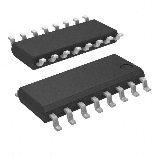
| 描述 | IC DUAL RS232 ESD-PROT 16-SOICRS-232接口集成电路 RS232 Line Driver/Receiver |
| Duplex | Full Duplex |
| 产品分类 | |
| 品牌 | Texas Instruments |
| 产品手册 | |
| 产品图片 |
|
| rohs | 符合RoHS无铅 / 符合限制有害物质指令(RoHS)规范要求 |
| 产品系列 | 接口 IC,RS-232接口集成电路,Texas Instruments MAX232EID- |
| 数据手册 | |
| 产品型号 | MAX232EID |
| 产品种类 | RS-232接口集成电路 |
| 传播延迟时间ns | 500 ns |
| 供应商器件封装 | 16-SOIC N |
| 关闭 | No |
| 其它名称 | 296-33360-5 |
| 功能 | Transceiver |
| 包装 | 管件 |
| 协议 | RS232 |
| 双工 | 全 |
| 商标 | Texas Instruments |
| 安装类型 | 表面贴装 |
| 安装风格 | SMD/SMT |
| 封装 | Tube |
| 封装/外壳 | 16-SOIC(0.154",3.90mm 宽) |
| 封装/箱体 | SOIC-16 |
| 工作温度 | -40°C ~ 85°C |
| 工作温度范围 | - 40 C to + 85 C |
| 工作电源电压 | 5 V |
| 工厂包装数量 | 40 |
| 接收器滞后 | 500mV |
| 接收机数量 | 2 Receiver |
| 数据速率 | 250kbps |
| 最大工作温度 | + 85 C |
| 最小工作温度 | - 40 C |
| 标准包装 | 40 |
| 激励器数量 | 2 Driver |
| 电压-电源 | 4.5 V ~ 5.5 V |
| 电源电流 | 10 mA |
| 类型 | 收发器 |
| 系列 | MAX232E |
| 输入/输出端数量 | 8 |
| 输入电压 | 5 V |
| 输出电压 | 0.3 V |
| 输出电流 | 10 mA |
| 驱动器/接收器数 | 2/2 |


PDF Datasheet 数据手册内容提取
Product Sample & Technical Tools & Support & Folder Buy Documents Software Community MAX232E SLLS723C–APRIL2006–REVISEDAUGUST2016 MAX232E Dual RS-232 Driver and Receiver With IEC61000-4-2 Protection 1 Features 3 Description • MeetsorExceedsTIA/RS-232-FandITU The MAX232E is a dual driver and receiver that 1 includes a capacitive voltage generator to supply RS- RecommendationV.28 232-F compliant voltage levels from a single 5-V • ESDProtectionforRS-232BusPins supply. Each receiver converts RS-232 inputs to 5-V – ±15-kVHuman-BodyModel(HBM) TTL/CMOS levels. This receiver has a typical – ±8-kVIEC61000-4-2,ContactDischarge threshold of 1.3 V, a typical hysteresis of 0.5 V, and can accept ±30-V inputs. Each driver converts – ±15-kVIEC61000-4-2,Air-GapDischarge TTL/CMOSinputlevelsintoTIA/RS-232-Flevels. • OperatesFromaSingle5-VPowerSupplyWith 1-µFCharge-PumpCapacitors DeviceInformation(1) • Operatesupto250kbit/s PARTNUMBER PACKAGE(PINS) BODYSIZE(NOM) • TwoDriversandTwoReceivers MAX232ECD SOIC(16) 9.90mm×3.91mm MAX232EID • LowSupplyCurrent:8mATypical MAX232ECDW SOICWIDE(16) 10.30mm×7.50mm MAX232EIDW 2 Applications MAX232ECN PDIP(16) 19.30mm×6.35mm • TIA/RS-232-F MAX232EIN • Battery-PoweredSystems MAX232ECPW TSSOP(16) 5.00mm×4.40mm MAX232EIPW • Terminals (1) For all available packages, see the orderable addendum at • Modems theendofthedatasheet. • Computers LogicDiagram(PositiveLogic) 5 V POWER DIN 2 TX 2 DOUT RS-232 250 kb/s IEC61000-4-2 2 2 RIN ROUT RX RS-232 Copyright © 2016,Texas Instruments Incorporated 1 An IMPORTANT NOTICE at the end of this data sheet addresses availability, warranty, changes, use in safety-critical applications, intellectualpropertymattersandotherimportantdisclaimers.PRODUCTIONDATA.
MAX232E SLLS723C–APRIL2006–REVISEDAUGUST2016 www.ti.com Table of Contents 1 Features.................................................................. 1 8.1 Overview...................................................................9 2 Applications........................................................... 1 8.2 FunctionalBlockDiagram.........................................9 3 Description............................................................. 1 8.3 FeatureDescription...................................................9 8.4 DeviceFunctionalModes........................................10 4 RevisionHistory..................................................... 2 9 ApplicationsandImplementation...................... 11 5 PinConfigurationandFunctions......................... 3 9.1 ApplicationInformation............................................11 6 Specifications......................................................... 4 9.2 TypicalApplication..................................................11 6.1 AbsoluteMaximumRatings......................................4 10 PowerSupplyRecommendations..................... 13 6.2 ESDRatings..............................................................4 11 Layout................................................................... 13 6.3 RecommendedOperatingConditions.......................4 6.4 ThermalInformation..................................................4 11.1 LayoutGuidelines.................................................13 6.5 ElectricalCharacteristics...........................................5 11.2 LayoutExample....................................................13 6.6 ElectricalCharacteristics:Driver...............................5 12 DeviceandDocumentationSupport................. 14 6.7 ElectricalCharacteristics:Receiver..........................5 12.1 ReceivingNotificationofDocumentationUpdates14 6.8 SwitchingCharacteristics:Driver..............................5 12.2 CommunityResources..........................................14 6.9 SwitchingCharacteristics:Receiver..........................6 12.3 Trademarks...........................................................14 6.10 TypicalCharacteristics............................................6 12.4 ElectrostaticDischargeCaution............................14 7 ParameterMeasurementInformation..................7 12.5 Glossary................................................................14 8 DetailedDescription.............................................. 9 13 Mechanical,Packaging,andOrderable Information........................................................... 14 4 Revision History NOTE:Pagenumbersforpreviousrevisionsmaydifferfrompagenumbersinthecurrentversion. ChangesfromRevisionB(November2009)toRevisionC Page • AddedESDRatingstable,FeatureDescriptionsection,DeviceFunctionalModes,ApplicationandImplementation section,PowerSupplyRecommendationssection,Layoutsection,DeviceandDocumentationSupportsection,and Mechanical,Packaging,andOrderableInformationsection ................................................................................................. 1 • Deleted"±30-VInputLevels"fromFeatures ......................................................................................................................... 1 • DeletedOrderingInformationtable;seePOAattheendofthedatasheet ......................................................................... 1 • AddedMINvalue±3to"Receiverinputvoltage(RIN1,RIN2)rowinRecommendedOperatingConditions.......................4 • ChangedR valuesinThermalInformation......................................................................................................................... 4 θJA • Deletedtablenote3fromReceiverSectionElectricalCharacteristics ................................................................................. 5 • AddedanewrowtotheFunctionTableforEachReceiver ................................................................................................ 10 2 SubmitDocumentationFeedback Copyright©2006–2016,TexasInstrumentsIncorporated ProductFolderLinks:MAX232E
MAX232E www.ti.com SLLS723C–APRIL2006–REVISEDAUGUST2016 5 Pin Configuration and Functions D,DW,N,orPWPackage Add16-PinSOIC,PDIP,orTSSOP TopView C1+ 1 16 VCC VS+ 2 15 GND C1− 3 14 DOUT1 C2+ 4 13 RIN1 C2− 5 12 ROUT1 V 6 11 DIN1 S− DOUT2 7 10 DIN2 RIN2 8 9 ROUT2 PinFunctions PIN I/O DESCRIPTION NO. NAME 1 C1+ — PositiveleadofC1capacitor 2 V O Positivechargepumpoutputforstoragecapacitoronly S+ 3 C1– — NegativeleadofC1capacitor 4 C2+ — PositiveleadofC2capacitor 5 C2– — NegativeleadofC2capacitor 6 V O Negativechargepumpoutputforstoragecapacitoronly S– 7 DOUT2 O RS-232linedataoutput(toremoteRS-232system) 8 RIN2 I RS-232linedatainput(fromremoteRS-232system) 9 ROUT2 O Logicdataoutput(toUART) 10 DIN2 I Logicdatainput(fromUART) 11 DIN1 I Logicdatainput(fromUART) 12 ROUT1 O Logicdataoutput(toUART) 13 RIN1 I RS-232linedatainput(fromremoteRS-232system) 14 DOUT1 O RS-232linedataoutput(toremoteRS-232system) 15 GND — Ground 16 V — Supplyvoltage—connecttoexternal5-Vpowersupply CC Copyright©2006–2016,TexasInstrumentsIncorporated SubmitDocumentationFeedback 3 ProductFolderLinks:MAX232E
MAX232E SLLS723C–APRIL2006–REVISEDAUGUST2016 www.ti.com 6 Specifications 6.1 Absolute Maximum Ratings overoperatingfree-airtemperaturerange(unlessotherwisenoted)(1) MIN MAX UNIT V Inputsupplyvoltage (2) –0.3 6 V CC V Positiveoutputsupplyvoltage V –0.3 15 V S+ CC V Negativeoutputsupplyvoltage –0.3 –15 V S– Driver –0.3 V +0.3 CC V Inputvoltage V I Receiver ±30 DOUT V –0.3 V +0.3 S– S+ V Outputvoltage V O ROUT –0.3 V +0.3 CC Short-circuitduration DOUT Unlimited T Operatingvirtualjunctiontemperature 150 °C J T Storagetemperature –65 150 °C stg (1) StressesbeyondthoselistedunderAbsoluteMaximumRatingsmaycausepermanentdamagetothedevice.Thesearestressratings only,whichdonotimplyfunctionaloperationofthedeviceattheseoranyotherconditionsbeyondthoseindicatedunderRecommended OperatingConditions.Exposuretoabsolute-maximum-ratedconditionsforextendedperiodsmayaffectdevicereliability. (2) AllvoltagesarewithrespecttonetworkGND. 6.2 ESD Ratings VALUE UNIT Pins7,8, ±15000 Human-bodymodel(HBM),perANSI/ESDA/JEDECJS-001(1) 13,and14 Otherpins ±3000 Electrostatic V(ESD) discharge Charged-devicemodel(CDM),perJEDECspecificationJESD22-C101(2) Allpins ±1500 V IEC61000-4-2,air-gapdischarge Pins7,8, ±15000 IEC61000-4-2,contactdischarge 13,and14 ±8000 (1) JEDECdocumentJEP155statesthat500-VHBMallowssafemanufacturingwithastandardESDcontrolprocess. (2) JEDECdocumentJEP157statesthat250-VCDMallowssafemanufacturingwithastandardESDcontrolprocess. 6.3 Recommended Operating Conditions MIN NOM MAX UNIT V Supplyvoltage 4.5 5 5.5 V CC V High-levelinputvoltage(DIN1,DIN2) 2 V IH V Low-levelinputvoltage(DIN1,DIN2) 0.8 V IL Receiverinputvoltage(RIN1,RIN2) ±3 ±30 V MAX232EC 0 70 T Operatingfree-airtemperature °C A MAX232EI –40 85 6.4 Thermal Information MAX232E THERMALMETRIC(1)(2)(3) D DW N PW UNIT (SOIC) (SOIC) (PDIP) (TSSOP) 16PINS 16PINS 16PINS 16PINS R Junction-to-ambientthermalresistance 73.8 73.4 43.3 101.6 °C/W θJA R Junction-to-case(top)thermalresistance 33.4 35.1 30 29.3 °C/W θJC(top) R Junction-to-boardthermalresistance 31.4 38.3 23.3 47.3 °C/W θJB (1) Formoreinformationabouttraditionalandnewthermalmetrics,seetheSemiconductorandICPackageThermalMetricsapplication report. (2) MaximumpowerdissipationisafunctionofT(max),R ,andT .Themaximumallowablepowerdissipationatanyallowableambient J θJA A temperatureisP =(T(max)–T )/R .OperatingattheabsolutemaximumT of150°Ccanaffectreliability. D J A θJA J (3) ThepackagethermalimpedanceiscalculatedinaccordancewithJESD51-7. 4 SubmitDocumentationFeedback Copyright©2006–2016,TexasInstrumentsIncorporated ProductFolderLinks:MAX232E
MAX232E www.ti.com SLLS723C–APRIL2006–REVISEDAUGUST2016 Thermal Information (continued) MAX232E THERMALMETRIC(1)(2)(3) D DW N PW UNIT (SOIC) (SOIC) (PDIP) (TSSOP) 16PINS 16PINS 16PINS 16PINS ψ Junction-to-topcharacterizationparameter 5.8 9.4 14.4 1.4 °C/W JT ψ Junction-to-boardcharacterizationparameter 31.1 37.7 23.2 46.6 °C/W JB 6.5 Electrical Characteristics overrecommendedrangesofsupplyvoltageandoperatingfree-airtemperature(unlessotherwisenoted)(seeFigure10) PARAMETER TESTCONDITIONS(1) MIN TYP(2) MAX UNIT I Supplycurrent V =5.5V Alloutputsopen,T =25°C 8 10 mA CC CC A (1) TestconditionsareC1–C4=1µFatV =5V±0.5V. CC (2) AlltypicalvaluesareatV =5VandT =25°C. CC A 6.6 Electrical Characteristics: Driver overrecommendedrangesofsupplyvoltageandoperatingfree-airtemperaturerange PARAMETER TESTCONDITIONS(1) MIN TYP(2) MAX UNIT V High-leveloutputvoltage DOUT R =3kΩtoGND 5 7 V OH L V Low-leveloutputvoltage(3) DOUT R =3kΩtoGND –7 –5 V OL L r Outputresistance DOUT V =V =0, V =±2V 300 Ω o S+ S– O I (4) Short-circuitoutputcurrent DOUT V =5.5V, V =0 ±10 mA OS CC O I Short-circuitinputcurrent DIN V =0 200 µA IS I (1) TestconditionsareC1–C4=1µFatV =5V±0.5V. CC (2) AlltypicalvaluesareatV =5VandT =25°C. CC A (3) Thealgebraicconvention,inwhichtheleast-positive(mostnegative)valueisdesignatedminimum,isusedinthisdatasheetforlogic voltagelevelsonly. (4) Notmorethanoneoutputshouldbeshortedatatime. 6.7 Electrical Characteristics: Receiver overrecommendedrangesofsupplyvoltageandoperatingfree-airtemperaturerange PARAMETER TESTCONDITIONS(1) MIN TYP(2) MAX UNIT V High-leveloutputvoltage ROUT I =–1mA 3.5 V OH OH V Low-leveloutputvoltage ROUT I =3.2mA 0.4 V OL OL V Receiverpositive-goinginputthresholdvoltage RIN V =5V T =25°C 1.7 2.4 V IT+ CC A V Receivernegative-goinginputthresholdvoltage RIN V =5V T =25°C 0.8 1.2 V IT– CC A V Inputhysteresisvoltage RIN V =5V 0.2 0.5 1 V hys CC r Receiverinputresistance RIN V =5V T =25°C 3 5 7 kΩ i CC A (1) TestconditionsareC1–C4=1µFatV =5V±0.5V. CC (2) AlltypicalvaluesareatV =5VandT =25°C. CC A 6.8 Switching Characteristics: Driver V =5V,T =25°C CC A PARAMETER TESTCONDITIONS(1) MIN TYP MAX UNIT SR Driverslewrate R =3kΩto7kΩ,SeeFigure6 30 V/µs L R =3kΩ,C =2.5nF SR(t) Drivertransitionregionslewrate L L 3 V/µs SeeFigure7 Datarate OneDOUTswitching 250 kbit/s (1) TestconditionsareC1–C4=1µFatV =5V±0.5V. CC Copyright©2006–2016,TexasInstrumentsIncorporated SubmitDocumentationFeedback 5 ProductFolderLinks:MAX232E
MAX232E SLLS723C–APRIL2006–REVISEDAUGUST2016 www.ti.com 6.9 Switching Characteristics: Receiver V =5V,T =25°C(seeFigure5) CC A PARAMETER TESTCONDITIONS(1) TYP UNIT t Receiverpropagationdelaytime,low-tohigh-leveloutput C =50pF 500 ns PLH(R) L t Receiverpropagationdelaytime,high-tolow-leveloutput C =50pF 500 ns PHL(R) L (1) TestconditionsareC1–C4=1µFatV =5V±0.5V. CC 6.10 Typical Characteristics T =25°C A 8 0.8 7 VOH 6 VOL 5 4 0.6 V) 3 V) e ( 2 e ( ag 1 ag olt 0 olt 0.4 T V -1 T V U -2 U O O D -3 R -4 0.2 -5 -6 -7 -8 0 1 2 3 4 5 6 7 8 9 10 0 1 2 3 4 5 6 7 8 9 10 DOUT Load Resistance (k:) ROUT Current (mA) D001 D002 Figure1.DriverOutputVoltagevsLoadResistance Figure2.ReceiverLowOutputVoltagevsLoadCurrent 6 12 DIN 10 DOUT 5 8 ROUT 6 V) 4 age ( m (V) 24 olt 3 or V ef 0 OUT 2 Wav -2 R -4 1 -6 -8 0 -10 0 1 2 3 4 5 6 7 8 9 10 0 5 10 15 20 ROUT Current (mA) Time (us) D003 D004 Figure3.ReceiverHighOutputVoltagevsLoadCurrent Figure4.LoopbackWaveforms DataRate120kbit/s 6 SubmitDocumentationFeedback Copyright©2006–2016,TexasInstrumentsIncorporated ProductFolderLinks:MAX232E
MAX232E www.ti.com SLLS723C–APRIL2006–REVISEDAUGUST2016 7 Parameter Measurement Information VCC RL= 1.3 kW Pulse RIN ROUT See Note C Generator (see NoteA) CL= 50 pF (see Note B) TEST CIRCUIT ≤10 ns ≤10 ns 3 V 90% 90% Input 10% 50% 50% 10% 0 V 500 ns tPHL tPLH VOH Output 1.5 V 1.5 V VOL WAVEFORMS A. Thepulsegeneratorhasthefollowingcharacteristics:Z =50Ω,dutycycle≤50%. O B. C includesprobeandjigcapacitance. L C. Alldiodesare1N3064orequivalent. Figure5. ReceiverTestCircuitandWaveformsfort andt Measurements PHL PLH Copyright©2006–2016,TexasInstrumentsIncorporated SubmitDocumentationFeedback 7 ProductFolderLinks:MAX232E
MAX232E SLLS723C–APRIL2006–REVISEDAUGUST2016 www.ti.com Parameter Measurement Information (continued) Pulse DIN DOUT Generator RS-232 Output (see NoteA) RL CL= 10 pF (see Note B) TEST CIRCUIT ≤10 ns ≤10 ns 3 V 90% 90% Input 50% 50% 10% 10% 0 V 5ms tPLH tPHL 90% 90% VOH Output 10% 10% VOL tTHL tTLH 0.8(V –V ) 0.8(V –V ) OH OL OL OH SR or t t TLH THL WAVEFORMS A. Thepulsegeneratorhasthefollowingcharacteristics:Z =50Ω,dutycycle≤50%. O B. C includesprobeandjigcapacitance. L Figure6. DriverTestCircuitandWaveformsfort andt Measurements(5-µsInput) PHL PLH Pulse DIN DOUT Generator RS-232 Output (see NoteA) 3 kW CL= 2.5 nF TEST CIRCUIT ≤10 ns ≤10 ns Input 90% 90% 10% 1.5 V 1.5 V 10% 20ms tTHL tTLH 3 V 3 V VOH Output −3 V −3 V VOL 6V SR t ort THL TLH WAVEFORMS A. Thepulsegeneratorhasthefollowingcharacteristics:Z =50Ω,dutycycle≤50%. O Figure7. TestCircuitandWaveformsfort andt Measurements(20-µsInput) THL TLH 8 SubmitDocumentationFeedback Copyright©2006–2016,TexasInstrumentsIncorporated ProductFolderLinks:MAX232E
MAX232E www.ti.com SLLS723C–APRIL2006–REVISEDAUGUST2016 8 Detailed Description 8.1 Overview The MAX232E device is a dual driver and receiver that includes a capacitive voltage generator using four capacitors to supply TIA/EIA-232-F voltage levels from a single 5-V supply. All RS-232 pins have 15-kV HBM and IEC61000-4-2 Air-Gap discharge protection. RS-232 pins also have 8-kV IEC61000-4-2 contact discharge protection. Each receiver converts TIA/EIA-232-F inputs to 5-V TTL/CMOS levels. These receivers have shorted and open fail safe. The receiver can accept up to ±30-V inputs and decode inputs as low as ±3 V. Each driver convertsTTL/CMOSinputlevelsintoTIA/EIA-232-Flevels.Outputsareprotectedagainstshortstoground. 8.2 Functional Block Diagram 5 V POWER DIN 2 TX 2 DOUT RS-232 250 kb/s IEC61000-4-2 2 2 RIN ROUT RX RS-232 Copyright © 2016,Texas Instruments Incorporated Figure8. LogicDiagram(PositiveLogic) 8.3 Feature Description 8.3.1 Power The power block increases and inverts the 5-V supply for the RS-232 driver using a charge pump that requires four1-µFexternalcapacitors. 8.3.2 RS-232Driver Two drivers interface standard logic level to RS-232 levels. Internal pullup resistors on DIN inputs ensures a high inputwhenthelineishighimpedance. 8.3.3 RS-232Receiver Two receivers interface RS-232 levels to standard logic levels. An open or shorted to ground input results in a highoutputonROUT. Copyright©2006–2016,TexasInstrumentsIncorporated SubmitDocumentationFeedback 9 ProductFolderLinks:MAX232E
MAX232E SLLS723C–APRIL2006–REVISEDAUGUST2016 www.ti.com 8.4 Device Functional Modes 8.4.1 V Poweredby5V CC Thedeviceisinnormaloperation. 8.4.2 V Unpowered CC WhenMAX232Eisunpowered,itcanbesafelyconnectedtoanactiveremoteRS-232device. 8.4.3 TruthTables Table1andTable2listthefunctionsofthisdevice. Table1.FunctionTablefor EachDriver(1) INPUT OUTPUT DIN DOUT L H H L (1) H=highlevel,L=lowlevel Table2.FunctionTablefor EachReceiver(1) INPUT OUTPUT RIN ROUT L H H L Open H (1) H=highlevel,L=lowlevel,Open =inputdisconnectedorconnected driveroff 11 14 DIN1 DOUT1 10 7 DIN2 DOUT2 12 13 ROUT1 RIN1 9 8 ROUT2 RIN2 Figure9. LogicDiagram(PositiveLogic) 10 SubmitDocumentationFeedback Copyright©2006–2016,TexasInstrumentsIncorporated ProductFolderLinks:MAX232E
MAX232E www.ti.com SLLS723C–APRIL2006–REVISEDAUGUST2016 9 Applications and Implementation NOTE Information in the following applications sections is not part of the TI component specification, and TI does not warrant its accuracy or completeness. TI’s customers are responsible for determining suitability of components for their purposes. Customers should validateandtesttheirdesignimplementationtoconfirmsystemfunctionality. 9.1 Application Information For proper operation add capacitors as shown in Figure 10. Pins 9 through 12 connect to UART or general purposelogiclines.RS-232linesonpins7,8,13,and14connecttoaconnectororcable. 9.2 Typical Application 5 V + CBYPASS= 1mF− 16 C3† 1mF VCC 1 2 C1 1mF 3 C1+ VS+ 8.5 V C1− 6 4 C2+ VS− −8.5 V C2 1mF 5 C4 1mF C2− + 11 14 RS-232 Output From CMOS or TTL 10 7 RS-232 Output 12 13 RS-232 Input To CMOS or TTL 9 8 RS-232 Input 0 V 15 GND †C3 can be connected to VCCor GND. Copyright © 2016,Texas Instruments Incorporated Resistorvaluesshownarenominal. Nonpolarizedceramiccapacitorsareacceptable.Ifpolarizedtantalumorelectrolyticcapacitorsareused,theyshould beconnectedasshown. Figure10. TypicalOperatingCircuit 9.2.1 DesignRequirements • V minimumis4.5Vandmaximumis5.5V. CC • Maximumrecommendedbitrateis250kbit/s. 9.2.2 DetailedDesignProcedure The capacitor type used for C1–C4 is not critical for proper operation. The MAX232E requires 1-µF capacitors, although capacitors up to 10 µF can be used without harm. Ceramic dielectrics are suggested for capacitors. When using the minimum recommended capacitor values, make sure the capacitance value does not degrade excessively as the operating temperature varies. If in doubt, use capacitors with a larger (for example, 2×) nominal value. The capacitors' effective series resistance (ESR), which usually rises at low temperatures, influencestheamountofrippleonV+andV–. Copyright©2006–2016,TexasInstrumentsIncorporated SubmitDocumentationFeedback 11 ProductFolderLinks:MAX232E
MAX232E SLLS723C–APRIL2006–REVISEDAUGUST2016 www.ti.com Typical Application (continued) Uselargercapacitors(upto10µF)toreducetheoutputimpedanceatV andV . S+ S– BypassV togroundwithatleast1µF.Inapplicationssensitivetopower-supplynoisegeneratedbythecharge CC pumps, decouple V to ground with a capacitor the same size as (or larger than) the charge-pump capacitors CC (C1–C4). 9.2.3 ApplicationCurve LoopbackwaveformconnectsDOUTtoRIN. 12 DIN 10 DOUT 8 ROUT 6 V) 4 m ( 2 or ef 0 v a W -2 -4 -6 -8 -10 0 5 10 15 20 Time (us) D005 DateRate=120kbit/s,C =1nF L Figure11.LoopbackWaveforms 12 SubmitDocumentationFeedback Copyright©2006–2016,TexasInstrumentsIncorporated ProductFolderLinks:MAX232E
MAX232E www.ti.com SLLS723C–APRIL2006–REVISEDAUGUST2016 10 Power Supply Recommendations The V voltage should be connected to the same power source used for logic device connected to DIN and CC ROUTpins.V shouldbebetween4.5Vand5.5V. CC 11 Layout 11.1 Layout Guidelines Keep the external capacitor traces short. This is more important on C1 and C2 nodes that have the fastest rise and fall times. Make the impedance from MAX232E ground pin and circuit board's ground plane as low as possibleforbestESDperformance.Usewidemetalandmultipleviasonbothsidesofgroundpin. 11.2 Layout Example Ground C3 1 C1+ VCC 16 VCC (cid:20)PF C1 2 V+ GND 15 Ground 3 C1- DOUT1 14 4 C2+ RIN1 13 C2 5 C2- ROUT1 12 Ground 6 V- DIN1 11 C4 7 DOUT2 DIN2 10 8 RIN2 ROUT2 9 Figure12. MAX232ELayout Copyright©2006–2016,TexasInstrumentsIncorporated SubmitDocumentationFeedback 13 ProductFolderLinks:MAX232E
MAX232E SLLS723C–APRIL2006–REVISEDAUGUST2016 www.ti.com 12 Device and Documentation Support 12.1 Receiving Notification of Documentation Updates To receive notification of documentation updates, navigate to the device product folder on ti.com. In the upper right corner, click on Alert me to register and receive a weekly digest of any product information that has changed.Forchangedetails,reviewtherevisionhistoryincludedinanyreviseddocument. 12.2 Community Resources The following links connect to TI community resources. Linked contents are provided "AS IS" by the respective contributors. They do not constitute TI specifications and do not necessarily reflect TI's views; see TI's Terms of Use. TIE2E™OnlineCommunity TI'sEngineer-to-Engineer(E2E)Community.Createdtofostercollaboration amongengineers.Ate2e.ti.com,youcanaskquestions,shareknowledge,exploreideasandhelp solveproblemswithfellowengineers. DesignSupport TI'sDesignSupport QuicklyfindhelpfulE2Eforumsalongwithdesignsupporttoolsand contactinformationfortechnicalsupport. 12.3 Trademarks E2EisatrademarkofTexasInstruments. Allothertrademarksarethepropertyoftheirrespectiveowners. 12.4 Electrostatic Discharge Caution This integrated circuit can be damaged by ESD. Texas Instruments recommends that all integrated circuits be handled with appropriateprecautions.Failuretoobserveproperhandlingandinstallationprocedurescancausedamage. ESDdamagecanrangefromsubtleperformancedegradationtocompletedevicefailure.Precisionintegratedcircuitsmaybemore susceptibletodamagebecauseverysmallparametricchangescouldcausethedevicenottomeetitspublishedspecifications. 12.5 Glossary SLYZ022—TIGlossary. Thisglossarylistsandexplainsterms,acronyms,anddefinitions. 13 Mechanical, Packaging, and Orderable Information The following pages include mechanical, packaging, and orderable information. This information is the most current data available for the designated devices. This data is subject to change without notice and revision of thisdocument.Forbrowser-basedversionsofthisdatasheet,refertotheleft-handnavigation. 14 SubmitDocumentationFeedback Copyright©2006–2016,TexasInstrumentsIncorporated ProductFolderLinks:MAX232E
PACKAGE OPTION ADDENDUM www.ti.com 6-Feb-2020 PACKAGING INFORMATION Orderable Device Status Package Type Package Pins Package Eco Plan Lead/Ball Finish MSL Peak Temp Op Temp (°C) Device Marking Samples (1) Drawing Qty (2) (6) (3) (4/5) MAX232ECD ACTIVE SOIC D 16 40 Green (RoHS NIPDAU Level-1-260C-UNLIM 0 to 70 MAX232EC & no Sb/Br) MAX232ECDR ACTIVE SOIC D 16 2500 Green (RoHS NIPDAU Level-1-260C-UNLIM 0 to 70 MAX232EC & no Sb/Br) MAX232ECDW ACTIVE SOIC DW 16 40 Green (RoHS NIPDAU Level-1-260C-UNLIM 0 to 70 MAX232EC & no Sb/Br) MAX232ECDWR ACTIVE SOIC DW 16 2000 Green (RoHS NIPDAU | SN Level-1-260C-UNLIM 0 to 70 MAX232EC & no Sb/Br) MAX232ECDWRE4 ACTIVE SOIC DW 16 2000 Green (RoHS NIPDAU Level-1-260C-UNLIM 0 to 70 MAX232EC & no Sb/Br) MAX232ECDWRG4 ACTIVE SOIC DW 16 2000 Green (RoHS NIPDAU Level-1-260C-UNLIM 0 to 70 MAX232EC & no Sb/Br) MAX232ECN ACTIVE PDIP N 16 25 Pb-Free NIPDAU N / A for Pkg Type 0 to 70 MAX232ECN (RoHS) MAX232ECNE4 ACTIVE PDIP N 16 25 Pb-Free NIPDAU N / A for Pkg Type 0 to 70 MAX232ECN (RoHS) MAX232ECPW ACTIVE TSSOP PW 16 90 Green (RoHS NIPDAU Level-1-260C-UNLIM 0 to 70 MA232EC & no Sb/Br) MAX232ECPWR ACTIVE TSSOP PW 16 2000 Green (RoHS NIPDAU | SN Level-1-260C-UNLIM 0 to 70 MA232EC & no Sb/Br) MAX232ECPWRG4 ACTIVE TSSOP PW 16 2000 Green (RoHS NIPDAU Level-1-260C-UNLIM 0 to 70 MA232EC & no Sb/Br) MAX232EID ACTIVE SOIC D 16 40 Green (RoHS NIPDAU Level-1-260C-UNLIM -40 to 85 MAX232EI & no Sb/Br) MAX232EIDR ACTIVE SOIC D 16 2500 Green (RoHS NIPDAU Level-1-260C-UNLIM -40 to 85 MAX232EI & no Sb/Br) MAX232EIDRG4 ACTIVE SOIC D 16 2500 Green (RoHS NIPDAU Level-1-260C-UNLIM -40 to 85 MAX232EI & no Sb/Br) MAX232EIDW ACTIVE SOIC DW 16 40 Green (RoHS NIPDAU Level-1-260C-UNLIM -40 to 85 MAX232EI & no Sb/Br) MAX232EIDWG4 ACTIVE SOIC DW 16 40 Green (RoHS NIPDAU Level-1-260C-UNLIM -40 to 85 MAX232EI & no Sb/Br) MAX232EIDWR ACTIVE SOIC DW 16 2000 Green (RoHS NIPDAU Level-1-260C-UNLIM -40 to 85 MAX232EI & no Sb/Br) Addendum-Page 1
PACKAGE OPTION ADDENDUM www.ti.com 6-Feb-2020 Orderable Device Status Package Type Package Pins Package Eco Plan Lead/Ball Finish MSL Peak Temp Op Temp (°C) Device Marking Samples (1) Drawing Qty (2) (6) (3) (4/5) MAX232EIN ACTIVE PDIP N 16 25 Pb-Free NIPDAU N / A for Pkg Type -40 to 85 MAX232EIN (RoHS) MAX232EINE4 ACTIVE PDIP N 16 25 Pb-Free NIPDAU N / A for Pkg Type -40 to 85 MAX232EIN (RoHS) MAX232EIPW ACTIVE TSSOP PW 16 90 Green (RoHS NIPDAU Level-1-260C-UNLIM -40 to 85 MB232EI & no Sb/Br) MAX232EIPWR ACTIVE TSSOP PW 16 2000 Green (RoHS NIPDAU Level-1-260C-UNLIM -40 to 85 MB232EI & no Sb/Br) (1) The marketing status values are defined as follows: ACTIVE: Product device recommended for new designs. LIFEBUY: TI has announced that the device will be discontinued, and a lifetime-buy period is in effect. NRND: Not recommended for new designs. Device is in production to support existing customers, but TI does not recommend using this part in a new design. PREVIEW: Device has been announced but is not in production. Samples may or may not be available. OBSOLETE: TI has discontinued the production of the device. (2) RoHS: TI defines "RoHS" to mean semiconductor products that are compliant with the current EU RoHS requirements for all 10 RoHS substances, including the requirement that RoHS substance do not exceed 0.1% by weight in homogeneous materials. Where designed to be soldered at high temperatures, "RoHS" products are suitable for use in specified lead-free processes. TI may reference these types of products as "Pb-Free". RoHS Exempt: TI defines "RoHS Exempt" to mean products that contain lead but are compliant with EU RoHS pursuant to a specific EU RoHS exemption. Green: TI defines "Green" to mean the content of Chlorine (Cl) and Bromine (Br) based flame retardants meet JS709B low halogen requirements of <=1000ppm threshold. Antimony trioxide based flame retardants must also meet the <=1000ppm threshold requirement. (3) MSL, Peak Temp. - The Moisture Sensitivity Level rating according to the JEDEC industry standard classifications, and peak solder temperature. (4) There may be additional marking, which relates to the logo, the lot trace code information, or the environmental category on the device. (5) Multiple Device Markings will be inside parentheses. Only one Device Marking contained in parentheses and separated by a "~" will appear on a device. If a line is indented then it is a continuation of the previous line and the two combined represent the entire Device Marking for that device. (6) Lead/Ball Finish - Orderable Devices may have multiple material finish options. Finish options are separated by a vertical ruled line. Lead/Ball Finish values may wrap to two lines if the finish value exceeds the maximum column width. Important Information and Disclaimer:The information provided on this page represents TI's knowledge and belief as of the date that it is provided. TI bases its knowledge and belief on information provided by third parties, and makes no representation or warranty as to the accuracy of such information. Efforts are underway to better integrate information from third parties. TI has taken and continues to take reasonable steps to provide representative and accurate information but may not have conducted destructive testing or chemical analysis on incoming materials and chemicals. TI and TI suppliers consider certain information to be proprietary, and thus CAS numbers and other limited information may not be available for release. Addendum-Page 2
PACKAGE OPTION ADDENDUM www.ti.com 6-Feb-2020 In no event shall TI's liability arising out of such information exceed the total purchase price of the TI part(s) at issue in this document sold by TI to Customer on an annual basis. Addendum-Page 3
PACKAGE MATERIALS INFORMATION www.ti.com 17-Apr-2020 TAPE AND REEL INFORMATION *Alldimensionsarenominal Device Package Package Pins SPQ Reel Reel A0 B0 K0 P1 W Pin1 Type Drawing Diameter Width (mm) (mm) (mm) (mm) (mm) Quadrant (mm) W1(mm) MAX232ECDR SOIC D 16 2500 330.0 16.4 6.5 10.3 2.1 8.0 16.0 Q1 MAX232ECDWR SOIC DW 16 2000 330.0 16.4 10.75 10.7 2.7 12.0 16.0 Q1 MAX232ECDWRG4 SOIC DW 16 2000 330.0 16.4 10.75 10.7 2.7 12.0 16.0 Q1 MAX232ECPWR TSSOP PW 16 2000 330.0 12.4 6.9 5.6 1.6 8.0 12.0 Q1 MAX232ECPWR TSSOP PW 16 2000 330.0 12.4 6.9 5.6 1.6 8.0 12.0 Q1 MAX232ECPWRG4 TSSOP PW 16 2000 330.0 12.4 6.9 5.6 1.6 8.0 12.0 Q1 MAX232EIDR SOIC D 16 2500 330.0 16.4 6.5 10.3 2.1 8.0 16.0 Q1 MAX232EIDWR SOIC DW 16 2000 330.0 16.4 10.75 10.7 2.7 12.0 16.0 Q1 MAX232EIPWR TSSOP PW 16 2000 330.0 12.4 6.9 5.6 1.6 8.0 12.0 Q1 PackMaterials-Page1
PACKAGE MATERIALS INFORMATION www.ti.com 17-Apr-2020 *Alldimensionsarenominal Device PackageType PackageDrawing Pins SPQ Length(mm) Width(mm) Height(mm) MAX232ECDR SOIC D 16 2500 367.0 367.0 38.0 MAX232ECDWR SOIC DW 16 2000 350.0 350.0 43.0 MAX232ECDWRG4 SOIC DW 16 2000 350.0 350.0 43.0 MAX232ECPWR TSSOP PW 16 2000 367.0 367.0 35.0 MAX232ECPWR TSSOP PW 16 2000 364.0 364.0 27.0 MAX232ECPWRG4 TSSOP PW 16 2000 367.0 367.0 35.0 MAX232EIDR SOIC D 16 2500 367.0 367.0 38.0 MAX232EIDWR SOIC DW 16 2000 350.0 350.0 43.0 MAX232EIPWR TSSOP PW 16 2000 367.0 367.0 35.0 PackMaterials-Page2
GENERIC PACKAGE VIEW DW 16 SOIC - 2.65 mm max height 7.5 x 10.3, 1.27 mm pitch SMALL OUTLINE INTEGRATED CIRCUIT This image is a representation of the package family, actual package may vary. Refer to the product data sheet for package details. 4224780/A www.ti.com
PACKAGE OUTLINE DW0016A SOIC - 2.65 mm max height SCALE 1.500 SOIC C 10.63 SEATING PLANE TYP 9.97 A PIN 1 ID 0.1 C AREA 14X 1.27 16 1 10.5 2X 10.1 8.89 NOTE 3 8 9 0.51 16X 0.31 7.6 B 7.4 0.25 C A B 2.65 MAX NOTE 4 0.33 TYP 0.10 SEE DETAIL A 0.25 GAGE PLANE 0.3 0 - 8 0.1 1.27 0.40 DETAIL A (1.4) TYPICAL 4220721/A 07/2016 NOTES: 1. All linear dimensions are in millimeters. Dimensions in parenthesis are for reference only. Dimensioning and tolerancing per ASME Y14.5M. 2. This drawing is subject to change without notice. 3. This dimension does not include mold flash, protrusions, or gate burrs. Mold flash, protrusions, or gate burrs shall not exceed 0.15 mm, per side. 4. This dimension does not include interlead flash. Interlead flash shall not exceed 0.25 mm, per side. 5. Reference JEDEC registration MS-013. www.ti.com
EXAMPLE BOARD LAYOUT DW0016A SOIC - 2.65 mm max height SOIC 16X (2) SEE SYMM DETAILS 1 16 16X (0.6) SYMM 14X (1.27) 8 9 R0.05 TYP (9.3) LAND PATTERN EXAMPLE SCALE:7X METAL SOLDER MASK SOLDER MASK METAL OPENING OPENING 0.07 MAX 0.07 MIN ALL AROUND ALL AROUND NON SOLDER MASK SOLDER MASK DEFINED DEFINED SOLDER MASK DETAILS 4220721/A 07/2016 NOTES: (continued) 6. Publication IPC-7351 may have alternate designs. 7. Solder mask tolerances between and around signal pads can vary based on board fabrication site. www.ti.com
EXAMPLE STENCIL DESIGN DW0016A SOIC - 2.65 mm max height SOIC 16X (2) SYMM 1 16 16X (0.6) SYMM 14X (1.27) 8 9 R0.05 TYP (9.3) SOLDER PASTE EXAMPLE BASED ON 0.125 mm THICK STENCIL SCALE:7X 4220721/A 07/2016 NOTES: (continued) 8. Laser cutting apertures with trapezoidal walls and rounded corners may offer better paste release. IPC-7525 may have alternate design recommendations. 9. Board assembly site may have different recommendations for stencil design. www.ti.com
None
None
PACKAGE OUTLINE PW0016A TSSOP - 1.2 mm max height SCALE 2.500 SMALL OUTLINE PACKAGE SEATING PLANE C 6.6 TYP 6.2 A 0.1 C PIN 1 INDEX AREA 14X 0.65 16 1 2X 5.1 4.55 4.9 NOTE 3 8 9 0.30 B 4.5 16X 0.19 1.2 MAX 4.3 0.1 C A B NOTE 4 (0.15) TYP SEE DETAIL A 0.25 GAGE PLANE 0.15 0.05 0.75 0.50 0 -8 DETA 20AIL A TYPICAL 4220204/A 02/2017 NOTES: 1. All linear dimensions are in millimeters. Any dimensions in parenthesis are for reference only. Dimensioning and tolerancing per ASME Y14.5M. 2. This drawing is subject to change without notice. 3. This dimension does not include mold flash, protrusions, or gate burrs. Mold flash, protrusions, or gate burrs shall not exceed 0.15 mm per side. 4. This dimension does not include interlead flash. Interlead flash shall not exceed 0.25 mm per side. 5. Reference JEDEC registration MO-153. www.ti.com
EXAMPLE BOARD LAYOUT PW0016A TSSOP - 1.2 mm max height SMALL OUTLINE PACKAGE 16X (1.5) SYMM (R0.05) TYP 1 16X (0.45) 16 SYMM 14X (0.65) 8 9 (5.8) LAND PATTERN EXAMPLE EXPOSED METAL SHOWN SCALE: 10X SOLDER MASK METAL UNDER SOLDER MASK OPENING METAL SOLDER MASK OPENING EXPOSED METAL EXPOSED METAL 0.05 MAX 0.05 MIN ALL AROUND ALL AROUND NON-SOLDER MASK SOLDER MASK DEFINED DEFINED (PREFERRED) SOLDE15.000R MASK DETAILS 4220204/A 02/2017 NOTES: (continued) 6. Publication IPC-7351 may have alternate designs. 7. Solder mask tolerances between and around signal pads can vary based on board fabrication site. www.ti.com
EXAMPLE STENCIL DESIGN PW0016A TSSOP - 1.2 mm max height SMALL OUTLINE PACKAGE 16X (1.5) SYMM (R0.05) TYP 1 16X (0.45) 16 SYMM 14X (0.65) 8 9 (5.8) SOLDER PASTE EXAMPLE BASED ON 0.125 mm THICK STENCIL SCALE: 10X 4220204/A 02/2017 NOTES: (continued) 8. Laser cutting apertures with trapezoidal walls and rounded corners may offer better paste release. IPC-7525 may have alternate design recommendations. 9. Board assembly site may have different recommendations for stencil design. www.ti.com
IMPORTANTNOTICEANDDISCLAIMER TI PROVIDES TECHNICAL AND RELIABILITY DATA (INCLUDING DATASHEETS), DESIGN RESOURCES (INCLUDING REFERENCE DESIGNS), APPLICATION OR OTHER DESIGN ADVICE, WEB TOOLS, SAFETY INFORMATION, AND OTHER RESOURCES “AS IS” AND WITH ALL FAULTS, AND DISCLAIMS ALL WARRANTIES, EXPRESS AND IMPLIED, INCLUDING WITHOUT LIMITATION ANY IMPLIED WARRANTIES OF MERCHANTABILITY, FITNESS FOR A PARTICULAR PURPOSE OR NON-INFRINGEMENT OF THIRD PARTY INTELLECTUAL PROPERTY RIGHTS. These resources are intended for skilled developers designing with TI products. You are solely responsible for (1) selecting the appropriate TI products for your application, (2) designing, validating and testing your application, and (3) ensuring your application meets applicable standards, and any other safety, security, or other requirements. These resources are subject to change without notice. TI grants you permission to use these resources only for development of an application that uses the TI products described in the resource. Other reproduction and display of these resources is prohibited. No license is granted to any other TI intellectual property right or to any third party intellectual property right. TI disclaims responsibility for, and you will fully indemnify TI and its representatives against, any claims, damages, costs, losses, and liabilities arising out of your use of these resources. TI’s products are provided subject to TI’s Terms of Sale (www.ti.com/legal/termsofsale.html) or other applicable terms available either on ti.com or provided in conjunction with such TI products. TI’s provision of these resources does not expand or otherwise alter TI’s applicable warranties or warranty disclaimers for TI products. Mailing Address: Texas Instruments, Post Office Box 655303, Dallas, Texas 75265 Copyright © 2020, Texas Instruments Incorporated