
 Datasheet下载
- 型号: SST25VF080B-80-4C-SAE
- 制造商: Microchip
- 库位|库存: xxxx|xxxx
- 要求:
| 数量阶梯 | 香港交货 | 国内含税 |
| +xxxx | $xxxx | ¥xxxx |
查看当月历史价格
查看今年历史价格
SST25VF080B-80-4C-SAE产品简介:
ICGOO电子元器件商城为您提供SST25VF080B-80-4C-SAE由Microchip设计生产,在icgoo商城现货销售,并且可以通过原厂、代理商等渠道进行代购。 SST25VF080B-80-4C-SAE价格参考。MicrochipSST25VF080B-80-4C-SAE封装/规格:存储器, FLASH 存储器 IC 8Mb (1M x 8) SPI 80MHz 8-SOIC。您可以下载SST25VF080B-80-4C-SAE参考资料、Datasheet数据手册功能说明书,资料中有SST25VF080B-80-4C-SAE 详细功能的应用电路图电压和使用方法及教程。
SST25VF080B-80-4C-SAE 是由 Microchip Technology 生产的一款串行闪存存储器,属于 SPI Flash 系列。以下是其主要应用场景:

1. 嵌入式系统:
   该型号常用于嵌入式系统中,作为代码存储和数据存储的解决方案。它可以存储微控制器或处理器所需的固件、引导程序(Bootloader)以及配置数据。

2. 工业自动化:
   在工业控制设备中,如 PLC(可编程逻辑控制器)、传感器模块和人机界面(HMI),SST25VF080B 提供可靠的数据存储能力,支持实时数据记录和参数保存。

3. 汽车电子:
   标注为“SAE”的后缀表明该器件适用于汽车电子环境。它可用于车载信息娱乐系统、仪表盘控制单元、发动机管理模块等,满足汽车行业对高温、高可靠性存储的需求。

4. 消费电子产品:
   在数字家电、智能手表、健身追踪器等消费类设备中,这款存储器可以保存用户设置、固件更新文件及运行时数据。

5. 通信设备:
   适用于路由器、调制解调器和其他网络设备,用于存储网络配置、协议栈和升级包。

6. 医疗设备:
   在便携式医疗设备(如血糖仪、心率监测仪)中,SST25VF080B 能够安全地存储患者的健康数据和设备校准信息。

7. 物联网(IoT)应用:
   该芯片适合低功耗 IoT 设备,例如智能家居节点、环境监测传感器,能够存储固件和采集的数据。

 特点与优势:
- 大容量:提供 8Mb(1MB)的存储空间,适合中小型应用程序。
- 高速读取:支持高达 50MHz 的 SPI 时钟频率,确保快速数据访问。
- 宽温度范围:工作温度范围为 -40°C 至 +125°C,适应恶劣环境。
- 低功耗设计:待机模式下电流极低,延长电池寿命。
- 高可靠性:具备 100,000 次擦写周期和长达 20 年的数据保持能力。

综上所述,SST25VF080B-80-4C-SAE 是一款功能强大且可靠的存储器,广泛应用于需要高性能、低功耗和高可靠性的领域。
| 参数 | 数值 |
| 产品目录 | 集成电路 (IC)半导体 |
| 描述 | IC FLASH 8MBIT 80MHZ 8SOIC闪存 2.7V to 3.6V 16Mbit SPI Serial 闪存 |
| 产品分类 | |
| 品牌 | Microchip Technology |
| 产品手册 | |
| 产品图片 |
|
| rohs | 符合RoHS无铅 / 符合限制有害物质指令(RoHS)规范要求 |
| 产品系列 | 内存,闪存,Microchip Technology SST25VF080B-80-4C-SAESST25 |
| 数据手册 | http://www.microchip.com/mymicrochip/filehandler.aspx?ddocname=en550441http://www.microchip.com/mymicrochip/filehandler.aspx?ddocname=en556157 |
| 产品型号 | SST25VF080B-80-4C-SAE |
| PCN组件/产地 | http://www.microchip.com/mymicrochip/NotificationDetails.aspx?id=5891&print=view |
| PCN设计/规格 | http://www.microchip.com/mymicrochip/NotificationDetails.aspx?id=5991&print=view |
| PCN过时产品 | http://www.microchip.com/mymicrochip/NotificationDetails.aspx?id=5675&print=view |
| 产品种类 | 闪存 |
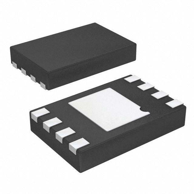
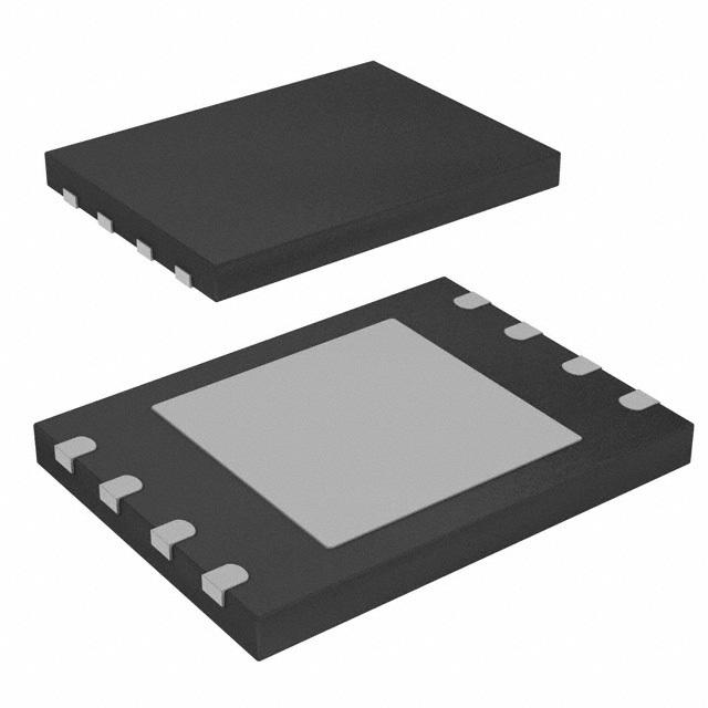
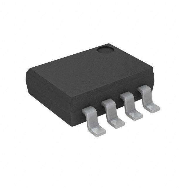
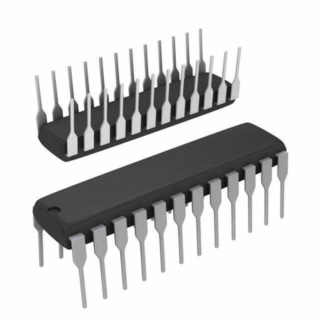
| 供应商器件封装 | 8-SOIC N |
| 包装 | 管件 |
| 商标 | Microchip Technology |
| 存储器类型 | FLASH |
| 存储容量 | 8 Mbit |
| 存储类型 | NOR |
| 安装风格 | SMD/SMT |
| 定时类型 | Synchronous |
| 封装 | Tube |
| 封装/外壳 | 8-SOIC(0.154",3.90mm 宽) |
| 封装/箱体 | SOIC-8 |
| 工作温度 | + 70 C |
| 工作温度范围 | 0 C to + 70 C |
| 工厂包装数量 | 100 |
| 接口 | SPI 串行 |
| 接口类型 | SPI |
| 数据总线宽度 | 8 bit |
| 最大工作电流 | 25 mA |
| 最大时钟频率 | 80 MHz |
| 标准包装 | 100 |
| 格式-存储器 | 闪存 |
| 电压-电源 | 2.7 V ~ 3.6 V |
| 电源电压-最大 | 3.6 V |
| 电源电压-最小 | 2.7 V |
| 系列 | SST25VF |
| 组织 | 1 M x 8 |
| 结构 | Sector |
| 速度 | 80 MHz |


- 商务部:美国ITC正式对集成电路等产品启动337调查
- 曝三星4nm工艺存在良率问题 高通将骁龙8 Gen1或转产台积电
- 太阳诱电将投资9.5亿元在常州建新厂生产MLCC 预计2023年完工
- 英特尔发布欧洲新工厂建设计划 深化IDM 2.0 战略
- 台积电先进制程称霸业界 有大客户加持明年业绩稳了
- 达到5530亿美元!SIA预计今年全球半导体销售额将创下新高
- 英特尔拟将自动驾驶子公司Mobileye上市 估值或超500亿美元
- 三星加码芯片和SET,合并消费电子和移动部门,撤换高东真等 CEO
- 三星电子宣布重大人事变动 还合并消费电子和移动部门
- 海关总署:前11个月进口集成电路产品价值2.52万亿元 增长14.8%


PDF Datasheet 数据手册内容提取
8 Mbit SPI Serial Flash SST25VF080B A Microchip Technology Company DataSheet SST's 25 series Serial Flash family features a four-wire, SPI-compatible interface that allows for a low pin-count package which occupies less board space and ulti- mately lowers total system costs. The SST25VF080B devices are enhanced with improved operating frequency and lower power consumption. SST25VF080B SPI serial flash memories are manufactured with SST's proprietary, high-performance CMOS SuperFlash technology. The split-gate cell design and thick-oxide tunnel- ing injector attain better reliability and manufacturability compared with alternate approaches. Features (cid:129) SingleVoltageReadandWriteOperations (cid:129) AutoAddressIncrement(AAI)Programming –2.7-3.6V –DecreasetotalchipprogrammingtimeoverByte-Pro- gramoperations (cid:129) SerialInterfaceArchitecture (cid:129) End-of-WriteDetection –SPICompatible:Mode0andMode3 –SoftwarepollingtheBUSYbitinStatusRegister (cid:129) HighSpeedClockFrequency –BusyStatusreadoutonSOpininAAIMode –50/66MHzconditional(seeTable14) (cid:129) HoldPin(HOLD#) -(SST25VF080B-50-xx-xxxx) –80MHz –Suspendsaserialsequencetothememory -(SST25VF080B-80-xx-xxxx) withoutdeselectingthedevice (cid:129) SuperiorReliability (cid:129) WriteProtection(WP#) –Endurance:100,000Cycles(typical) –Enables/DisablestheLock-Downfunctionofthestatus –Greaterthan100yearsDataRetention register (cid:129) LowPowerConsumption: (cid:129) SoftwareWriteProtection –ActiveReadCurrent:10mA(typical) –WriteprotectionthroughBlock-Protectionbitsinstatus –StandbyCurrent:5µA(typical) register (cid:129) FlexibleEraseCapability (cid:129) TemperatureRange –Uniform4KBytesectors –Commercial:0°Cto+70°C –Uniform32KByteoverlayblocks –Industrial:-40°Cto+85°C –Uniform64KByteoverlayblocks (cid:129) PackagesAvailable (cid:129) FastEraseandByte-Program: –8-leadSOIC(200mils) –Chip-EraseTime:35ms(typical) –8-leadSOIC(150mils) –Sector-/Block-EraseTime:18ms(typical) –8-contactWSON(6mmx5mm) –Byte-ProgramTime:7µs(typical) –8-leadPDIP(300mils) (cid:129) AlldevicesareRoHScompliant www.microchip.com ©2011SiliconStorageTechnology,Inc. DS25045A 09/11
8 Mbit SPI Serial Flash SST25VF080B A Microchip Technology Company DataSheet Product Description SST’s25seriesSerialFlashfamilyfeaturesafour-wire,SPI-compatibleinterfacethatallowsforalow pin-count package which occupies less board space and ultimately lowers total system costs. The SST25VF080B devices are enhanced with improved operating frequency and lower power consump- tion. SST25VF080B SPI serial flash memories are manufactured with SST’s proprietary, high-perfor- mance CMOS SuperFlash technology. The split-gate cell design and thick-oxide tunneling injector attainbetterreliabilityandmanufacturabilitycomparedwithalternateapproaches. The SST25VF080B devices significantly improve performance and reliability, while lowering power consumption. The devices write (Program or Erase) with a single power supply of 2.7-3.6V for SST25VF080B. The total energy consumed is a function of the applied voltage, current, and time of application. Since for any given voltage range, the SuperFlash technology uses less current to pro- gramandhasashortererasetime,thetotalenergyconsumedduringanyEraseorProgramoperation islessthanalternativeflashmemorytechnologies. The SST25VF080B device is offered in 8-lead SOIC (200 mils), 8-lead SOIC (150 mils), 8-contact WSON(6mmx5mm),and8-leadPDIP(300mils)packages.SeeFigure2forpinassignments. ©2011SiliconStorageTechnology,Inc. DS25045A 09/11 2
8 Mbit SPI Serial Flash SST25VF080B A Microchip Technology Company DataSheet Block Diagram SuperFlash X - Decoder Address Memory Buffers and Latches Y - Decoder I/O Buffers Control Logic and Data Latches Serial Interface 1296B1.0 CE# SCK SI SO WP# HOLD# Figure 1: Functional Block Diagram ©2011SiliconStorageTechnology,Inc. DS25045A 09/11 3
8 Mbit SPI Serial Flash SST25VF080B A Microchip Technology Company DataSheet Pin Description CE# 1 8 VDD CE# 1 8 VDD SO 2 7 HOLD# SO 2 7 HOLD# TopView TopView WP# 3 6 SCK WP# 3 6 SCK VSS 4 5 SI VSS 4 5 SI 129608-soicS2AP1.0 129608-wsonQAP2.0 8-leadSOIC 8-contactWSON CE# VDD SO TopView HOLD# WP# SCK VSS SI 129608-pdip-PA-P3.0 8-leadPDIP Figure 2: Pin Assignments Table 1: Pin Description Symbol PinName Functions SCK SerialClock Toprovidethetimingoftheserialinterface. Commands,addresses,orinputdataarelatchedontherisingedgeoftheclock input,whileoutputdataisshiftedoutonthefallingedgeoftheclockinput. SI SerialDataInput Totransfercommands,addresses,ordataseriallyintothedevice. Inputsarelatchedontherisingedgeoftheserialclock. SO SerialDataOutput Totransferdataseriallyoutofthedevice. Dataisshiftedoutonthefallingedgeoftheserialclock. OutputsFlashbusystatusduringAAIProgrammingwhenreconfiguredasRY/ BY#pin.See“HardwareEnd-of-WriteDetection”onpage13fordetails. CE# ChipEnable ThedeviceisenabledbyahightolowtransitiononCE#.CE#mustremainlow forthedurationofanycommandsequence. WP# WriteProtect TheWriteProtect(WP#)pinisusedtoenable/disableBPLbitinthestatusregister. HOLD# Hold TotemporarilystopserialcommunicationwithSPIflashmemorywithoutreset- tingthedevice. V PowerSupply Toprovidepowersupplyvoltage: 2.7-3.6VforSST25VF080B DD V Ground SS T1.025045 ©2011SiliconStorageTechnology,Inc. DS25045A 09/11 4
8 Mbit SPI Serial Flash SST25VF080B A Microchip Technology Company DataSheet Memory Organization TheSST25VF080BSuperFlashmemoryarrayisorganizedinuniform4KByteerasablesectorswith32 KByteoverlayblocksand64KByteoverlayerasableblocks. Device Operation TheSST25VF080BisaccessedthroughtheSPI(SerialPeripheralInterface)buscompatibleprotocol. The SPI bus consist of four control lines; Chip Enable (CE#) is used to select the device, and data is accessedthroughtheSerialDataInput(SI),SerialDataOutput(SO),andSerialClock(SCK). TheSST25VF080BsupportsbothMode0(0,0)andMode3(1,1)ofSPIbusoperations.Thedifference betweenthetwomodes,asshowninFigure3,isthestateoftheSCKsignalwhenthebusmasterisin Stand-bymodeandnodataisbeingtransferred.TheSCKsignalislowforMode0andSCKsignalis highforMode3.Forbothmodes,theSerialDataIn(SI)issampledattherisingedgeoftheSCKclock signalandtheSerialDataOutput(SO)isdrivenafterthefallingedgeoftheSCKclocksignal. CE# MODE3 MODE3 SCK MODE0 MODE0 SI Bit7 Bit6 Bit5 Bit4 Bit3 Bit2 Bit1 Bit0 DONTCARE MSB HIGHIMPEDANCE Bit7 Bit6 Bit5 Bit4 Bit3 Bit2 Bit1 Bit0 SO MSB 1296SPIprot.0 Figure 3: SPI Protocol ©2011SiliconStorageTechnology,Inc. DS25045A 09/11 5
8 Mbit SPI Serial Flash SST25VF080B A Microchip Technology Company DataSheet Hold Operation TheHOLD#pinisusedtopauseaserialsequenceunderwaywiththeSPIflashmemorywithoutreset- tingtheclockingsequence.ToactivatetheHOLD#mode,CE#mustbeinactivelowstate.TheHOLD# modebeginswhentheSCKactivelowstatecoincideswiththefallingedgeoftheHOLD#signal.The HOLDmodeendswhentheHOLD#signal’srisingedgecoincideswiththeSCKactivelowstate. IfthefallingedgeoftheHOLD#signaldoesnotcoincidewiththeSCKactivelowstate,thenthedevice enters Hold mode when the SCK next reaches the active low state. Similarly, if the rising edge of the HOLD# signal does not coincide with the SCK active low state, then the device exits in Hold mode whentheSCKnextreachestheactivelowstate.SeeFigure4forHoldConditionwaveform. OncethedeviceentersHoldmode,SOwillbeinhigh-impedancestatewhileSIandSCKcanbeV orV IL IH. If CE# is driven active high during a Hold condition, it resets the internal logic of the device. As long as HOLD#signalislow,thememoryremainsintheHoldcondition.Toresumecommunicationwiththedevice, HOLD#mustbedrivenactivehigh,andCE#mustbedrivenactivelow.SeeFigure24forHoldtiming. SCK HOLD# Active Hold Active Hold Active 1296HoldCond.0 Figure 4: Hold Condition Waveform Write Protection SST25VF080B provides software Write protection. The Write Protect pin (WP#) enables or disables thelock-downfunctionofthestatusregister.TheBlock-Protectionbits(BP3,BP2,BP1,BP0,andBPL) inthestatusregisterprovideWriteprotectiontothememoryarrayandthestatusregister.SeeTable4 fortheBlock-Protectiondescription. Write Protect Pin (WP#) The Write Protect (WP#) pin enables the lock-down function of the BPL bit (bit 7) in the status register. WhenWP#isdrivenlow,theexecutionoftheWrite-Status-Register(WRSR)instructionisdeterminedby thevalueoftheBPLbit(seeTable2).WhenWP#ishigh,thelock-downfunctionoftheBPLbitisdisabled. Table 2: Conditions to execute Write-Status-Register (WRSR) Instruction WP# BPL ExecuteWRSRInstruction L 1 NotAllowed L 0 Allowed H X Allowed T2.025045 ©2011SiliconStorageTechnology,Inc. DS25045A 09/11 6
8 Mbit SPI Serial Flash SST25VF080B A Microchip Technology Company DataSheet Status Register The software status register provides status on whether the flash memory array is available for any ReadorWriteoperation,whetherthedeviceisWriteenabled,andthestateoftheMemoryWritepro- tection. During an internal Erase or Program operation, the status register may be read only to deter- mine the completion of an operation in progress. Table 3 describes the function of each bit in the softwarestatusregister. Table 3: Software Status Register Defaultat Bit Name Function Power-up Read/Write 0 BUSY 1=InternalWriteoperationisinprogress 0 R 0=NointernalWriteoperationisinprogress 1 WEL 1=DeviceismemoryWriteenabled 0 R 0=DeviceisnotmemoryWriteenabled 2 BP0 Indicatecurrentlevelofblockwriteprotection(SeeTable4) 1 R/W 3 BP1 Indicatecurrentlevelofblockwriteprotection(SeeTable4) 1 R/W 4 BP2 Indicatecurrentlevelofblockwriteprotection(SeeTable4) 1 R/W 5 BP3 Indicatecurrentlevelofblockwriteprotection(SeeTable4) 0 R/W 6 AAI AutoAddressIncrementProgrammingstatus 0 R 1=AAIprogrammingmode 0=Byte-Programmode 7 BPL 1=BP3,BP2,BP1,BP0areread-onlybits 0 R/W 0=BP3,BP2,BP1,BP0areread/writable T3.0 25045 Busy TheBusybitdetermineswhetherthereisaninternalEraseorProgramoperationinprogress.A“1”for the Busy bit indicates the device is busy with an operation in progress. A “0” indicates the device is readyforthenextvalidoperation. Write Enable Latch (WEL) The Write-Enable-Latch bit indicates the status of the internal memory Write Enable Latch. If the Write-Enable-Latchbitissetto“1”,itindicatesthedeviceisWriteenabled.Ifthebitissetto“0”(reset), it indicates the device is not Write enabled and does not accept any memory Write (Program/Erase) commands.TheWrite-Enable-Latchbitisautomaticallyresetunderthefollowingconditions: (cid:129) Power-up (cid:129) Write-Disable(WRDI)instructioncompletion (cid:129) Byte-Programinstructioncompletion (cid:129) AutoAddressIncrement(AAI)programmingiscompletedorreacheditshighestunpro- tectedmemoryaddress (cid:129) Sector-Eraseinstructioncompletion (cid:129) Block-Eraseinstructioncompletion (cid:129) Chip-Eraseinstructioncompletion (cid:129) Write-Status-Registerinstructions ©2011SiliconStorageTechnology,Inc. DS25045A 09/11 7
8 Mbit SPI Serial Flash SST25VF080B A Microchip Technology Company DataSheet Auto Address Increment (AAI) The Auto Address Increment Programming-Status bit provides status on whether the device is in AAI programmingmodeorByte-Programmode.ThedefaultatpowerupisByte-Programmode. Block Protection (BP3,BP2, BP1, BP0) The Block-Protection (BP3, BP2, BP1, BP0) bits define the size of the memory area, as defined in Table4,tobesoftwareprotectedagainstanymemoryWrite(ProgramorErase)operation.TheWrite- Status-Register (WRSR) instruction is used to program the BP3, BP2, BP1 and BP0 bits as long as WP#ishighortheBlock-Protect-Lock(BPL)bitis0.Chip-ErasecanonlybeexecutedifBlock-Protec- tionbitsareall0.Afterpower-up,BP3,BP2,BP1andBP0aresetto1. Block Protection Lock-Down (BPL) WP# pin driven low (V ), enables the Block-Protection-Lock-Down (BPL) bit. When BPL is set to 1, it IL preventsanyfurtheralterationoftheBPL,BP3,BP2,BP1,andBP0bits.WhentheWP#pinisdriven high(V ),theBPLbithasnoeffectanditsvalueis“Don’tCare”.Afterpower-up,theBPLbitisresetto IH 0. Table 4: Software Status Register Block Protection forSST25VF080B1 StatusRegisterBit2 ProtectedMemoryAddress ProtectionLevel BP3 BP2 BP1 BP0 8Mbit None X 0 0 0 None Upper1/16 X 0 0 1 F0000H-FFFFFH Upper1/8 X 0 1 0 E0000H-FFFFFH Upper1/4 X 0 1 1 C0000H-FFFFFH Upper1/2 X 1 0 0 80000H-FFFFFH AllBlocks X 1 0 1 00000H-FFFFFH AllBlocks X 1 1 0 00000H-FFFFFH AllBlocks X 1 1 1 00000H-FFFFFH T4.025045 1. X=Don’tCare(RESERVED)defaultis“0 2. Defaultatpower-upforBP2,BP1,andBP0is‘111’.(AllBlocksProtected) ©2011SiliconStorageTechnology,Inc. DS25045A 09/11 8
8 Mbit SPI Serial Flash SST25VF080B A Microchip Technology Company DataSheet Instructions Instructions are used to read, write (Erase and Program), and configure the SST25VF080B. The instructionbuscyclesare8bitseachforcommands(OpCode),data,andaddresses.Priortoexecut- inganyByte-Program,AutoAddressIncrement(AAI)programming,Sector-Erase,Block-Erase,Write- Status-Register, or Chip-Erase instructions, the Write-Enable (WREN) instruction must be executed first.ThecompletelistofinstructionsisprovidedinTable5.Allinstructionsaresynchronizedoffahigh tolowtransitionofCE#.InputswillbeacceptedontherisingedgeofSCKstartingwiththemostsignif- icantbit.CE#mustbedrivenlowbeforeaninstructionisenteredandmustbedrivenhighafterthelast bitoftheinstructionhasbeenshiftedin(exceptforRead,Read-ID,andRead-Status-Registerinstruc- tions). Any low to high transition on CE#, before receiving the last bit of an instruction bus cycle, will terminate the instruction in progress and return the device to standby mode. Instruction commands (OpCode),addresses,anddataareallinputfromthemostsignificantbit(MSB)first. Table 5: Device Operation Instructions Address Dummy Data Instruction Description OpCodeCycle1 Cycle(s)2 Cycle(s) Cycle(s) Read ReadMemory 00000011b(03H) 3 0 1to High-SpeedRead ReadMemoryathigher 00001011b(0BH) 3 1 1to speed 4KByteSector-Erase3 Erase4KByteof 00100000b(20H) 3 0 0 memoryarray 32KByteBlock-Erase4 Erase32KByteblock 01010010b(52H) 3 0 0 ofmemoryarray 64KByteBlock-Erase5 Erase64KByteblock 11011000b(D8H) 3 0 0 ofmemoryarray Chip-Erase EraseFullMemoryArray 01100000b(60H)or 0 0 0 11000111b(C7H) Byte-Program ToProgramOneDataByte 00000010b(02H) 3 0 1 AAI-Word-Program6 AutoAddressIncrement 10101101b(ADH) 3 0 2to Programming RDSR7 Read-Status-Register 00000101b(05H) 0 0 1to EWSR Enable-Write-Status-Register 0101b0000b(50H) 0 0 0 WRSR Write-Status-Register 00000001b(01H) 0 0 1 WREN Write-Enable 00000110b(06H) 0 0 0 WRDI Write-Disable 00000100b(04H) 0 0 0 RDID8 Read-ID 10010000b(90H)or 3 0 1to 10101011b(ABH) JEDEC-ID JEDECIDread 10011111b(9FH) 0 0 3to EBSY EnableSOtooutputRY/BY# 01110000b(70H) 0 0 0 statusduringAAIprogramming DBSY DisableSOasRY/BY# 10000000b(80H) 0 0 0 statusduringAAIprogramming T5.0 25045 1. Onebuscycleiseightclockperiods. 2. AddressbitsabovethemostsignificantbitofeachdensitycanbeVILorVIH. 3. 4KByteSectorEraseaddresses:useAMS-A12,remainingaddressesaredon’tcarebutmustbeseteitheratVILorVIH. 4. 32KByteBlockEraseaddresses:useAMS-A15,remainingaddressesaredon’tcarebutmustbeseteitheratVILorVIH. 5. 64KByteBlockEraseaddresses:useAMS-A16,remainingaddressesaredon’tcarebutmustbeseteitheratVILorVIH. ©2011SiliconStorageTechnology,Inc. DS25045A 09/11 9
8 Mbit SPI Serial Flash SST25VF080B A Microchip Technology Company DataSheet 6. Tocontinueprogrammingtothenextsequentialaddresslocation,enterthe8-bitcommand,ADH,followedby2bytesof datatobeprogrammed.DataByte0willbeprogrammedintotheinitialaddress[A23-A1]withA0=0,DataByte1willbe programmedintothe initialaddress[A23-A1]withA0=1. 7. TheRead-Status-RegisteriscontinuouswithongoingclockcyclesuntilterminatedbyalowtohightransitiononCE#. 8. Manufacturer’sIDisreadwithA0=0,andDeviceIDisreadwithA0=1.Allotheraddressbitsare00H.TheManufac- turer’sIDanddeviceIDoutputstreamiscontinuousuntilterminatedbyalow-to-hightransitiononCE#. Read (25/33 MHz) The Read instruction, 03H, supports up to 25 MHz (for SST25VF080B-50-xx-xxxx) or 33 MHz (for SST25VF080B-80-xx-xxxx) Read. The device outputs the data starting from the specified address location. The data output stream is continuous through all addressesuntil terminated by a low to high transition on CE#. The internal address pointer will automatically increment until the highest memory address is reached. Once the highest memory address is reached, the address pointer will automati- cally increment to the beginning (wrap-around) of the address space. Once the data from address location1FFFFFHhasbeenread,thenextoutputwillbefromaddresslocation000000H. The Read instruction is initiated by executing an 8-bit command, 03H, followed by address bits [A23- A0]. CE# must remain active low for the duration of the Read cycle. See Figure 5 for the Read sequence. CE# MODE3 0 1 2 3 4 5 6 7 8 1516 2324 3132 3940 47 48 5556 6364 70 SCK MODE0 SI 03 ADD. ADD. ADD. MSB MSB N N+1 N+2 N+3 N+4 HIGHIMPEDANCE SO DOUT DOUT DOUT DOUT DOUT MSB 1296ReadSeq0.0 Figure 5: Read Sequence ©2011SiliconStorageTechnology,Inc. DS25045A 09/11 10
8 Mbit SPI Serial Flash SST25VF080B A Microchip Technology Company DataSheet High-Speed-Read (66/80 MHz) TheHigh-Speed-Readinstructionsupportingupto66MHz(forSST25VF080B-50-xx-xxxx)or80MHz (for SST25VF040B-80-xx-xxxx) Read is initiated by executing an 8-bit command, 0BH, followed by address bits [A23-A0] and a dummy byte. CE# must remain active low for the duration of the High- Speed-Readcycle.SeeFigure6fortheHigh-Speed-Readsequence. Following a dummy cycle, the High-Speed-Read instruction outputs the data starting from the speci- fiedaddresslocation.Thedataoutputstreamiscontinuousthroughalladdressesuntilterminatedbya low to high transition on CE#. The internal address pointer will automatically increment until the high- est memory address is reached. Once the highest memory address is reached, the address pointer willautomaticallyincrementtothebeginning(wrap-around)oftheaddressspace.Oncethedatafrom addresslocationFFFFFHhasbeenread,thenextoutputwillbefromaddresslocation00000H. CE# MODE3 0 1 2 3 4 5 6 7 8 1516 23 24 3132 3940 4748 55 56 6364 7172 80 SCK MODE0 SI 0B ADD. ADD. ADD. X MSB MSB N N+1 N+2 N+3 N+4 HIGHIMPEDANCE SO DOUT DOUT DOUT DOUT DOUT MSB 1296HSRdSeq.0 Note: X=DummyByte:8ClocksInputDummyCycle(VILorVIH) Figure 6: High-Speed-Read Sequence ©2011SiliconStorageTechnology,Inc. DS25045A 09/11 11
8 Mbit SPI Serial Flash SST25VF080B A Microchip Technology Company DataSheet Byte-Program TheByte-Programinstructionprogramsthebitsintheselectedbytetothedesireddata.Theselected bytemust beinthe erasedstate(FFH) wheninitiatinga Program operation. AByte-Programinstruction appliedtoaprotectedmemoryareawillbeignored. PriortoanyWriteoperation,theWrite-Enable(WREN)instructionmustbeexecuted.CE#mustremain activelowforthedurationoftheByte-Programinstruction.TheByte-Programinstructionisinitiatedby executingan8-bitcommand,02H,followedbyaddressbits[A -A ].Followingtheaddress,thedatais 23 0 input in order from MSB (bit 7) to LSB (bit 0). CE# must be driven high before the instruction is exe- cuted. The user may poll the Busy bit in the software status register or wait T for the completion of BP theinternalself-timedByte-Programoperation.SeeFigure7fortheByte-Programsequence. CE# MODE3 0 1 2 3 4 5 6 7 8 1516 2324 3132 39 SCK MODE0 SI 02 ADD. ADD. ADD. DIN MSB MSB MSB LSB SO HIGHIMPEDANCE 1296ByteProg.0 Figure 7: Byte-Program Sequence ©2011SiliconStorageTechnology,Inc. DS25045A 09/11 12
8 Mbit SPI Serial Flash SST25VF080B A Microchip Technology Company DataSheet Auto Address Increment (AAI) Word-Program The AAI program instruction allows multiple bytes of data to be programmed without re-issuing the next sequential address location. This feature decreases total programming time when multiple bytes orentirememoryarrayistobeprogrammed.AnAAIWordprograminstructionpointingtoaprotected memoryareawillbeignored.Theselectedaddressrangemustbeintheerasedstate(FFH)whenini- tiating an AAI Word Program operation. While within AAI Word Programming sequence, only the fol- lowing instructions are valid: for software end-of-write detection—AAI Word (ADH), WRDI (04H), and RDSR(05H);forhardwareend-of-writedetection—AAIWord(ADH)andWRDI(04H).Therearethree options to determine the completion of each AAI Word program cycle: hardware detection by reading theSerialOutput,softwaredetectionbypollingtheBUSYbitinthesoftwarestatusregister,orwaitT BP. Referto“End-of-WriteDetection”fordetails. Prior to any write operation, the Write-Enable (WREN) instruction must be executed. Initiate the AAI WordPrograminstructionbyexecutingan8-bitcommand,ADH,followedbyaddressbits[A -A ].Fol- 23 0 lowingtheaddresses,twobytesofdataareinputsequentially,eachonefromMSB(Bit7)toLSB(Bit 0). The first byte of data (D0) is programmed into the initial address [A -A ] with A =0, the second 23 1 0 byte of Data (D1) is programmed into the initial address [A -A ] with A =1. CE# must be driven high 23 1 0 before executing the AAI Word Program instruction. Check the BUSY status before entering the next valid command. Once the device indicates it is no longer busy, data for the next two sequential addressesmaybeprogrammed,followedbythenexttwo,andsoon. Whenprogrammingthelastdesiredword,orthehighestunprotectedmemoryaddress,checkthebusy statususingeitherthehardwareorsoftware(RDSRinstruction)methodtocheckforprogramcomple- tion. Once programming is complete, use the applicable method to terminate AAI. If the device is in Software End-of-Write Detection mode, execute the Write-Disable (WRDI) instruction, 04H. If the deviceisinAAIHardwareEnd-of-WriteDetectionmode,executetheWrite-Disable(WRDI)instruction, 04H, followed by the 8-bit DBSY command, 80H. There is no wrap mode during AAI programming once the highest unprotected memory address is reached. See Figures 10 and 11 for the AAI Word programmingsequence. End-of-Write Detection There are three methods to determine completion of a program cycle during AAI Word programming: hardwaredetectionbyreadingtheSerialOutput,softwaredetectionbypollingtheBUSYbitintheSoft- ware Status Register, or wait T The Hardware End-of-Write detection method is described in the BP. sectionbelow. Hardware End-of-Write Detection The Hardware End-of-Write detection method eliminates the overhead of polling the Busy bit in the SoftwareStatusRegisterduringanAAIWordprogramoperation.The8-bitcommand,70H,configures theSerialOutput(SO)pintoindicateFlashBusystatusduringAAIWordprogramming.(seeFigure8) The8-bit command, 70H,must be executed prior toinitiating an AAIWord-Program instruction.Once aninternalprogrammingoperationbegins,assertingCE#willimmediatelydrivethestatusoftheinter- nalflashstatusontheSOpin.A‘0’indicatesthedeviceisbusyanda‘1’indicatesthedeviceisready forthenextinstruction.De-assertingCE#willreturntheSOpintotri-state.WhileinAAIandHardware End-of-Writedetectionmode,theonlyvalidinstructionsareAAIWord(ADH)andWRDI(04H). To exit AAI Hardware End-of-Write detection, first execute WRDI instruction, 04H, to reset the Write- Enable-Latch bit (WEL=0) and AAI bit. Then execute the 8-bit DBSY command, 80H, to disable RY/ BY#statusduringtheAAIcommand.SeeFigures9and10. ©2011SiliconStorageTechnology,Inc. DS25045A 09/11 13
8 Mbit SPI Serial Flash SST25VF080B A Microchip Technology Company DataSheet CE# MODE3 0 1 2 3 4 5 6 7 SCK MODE0 SI 70 MSB SO HIGHIMPEDANCE 1296EnableSO.0 Figure 8: Enable SO as Hardware RY/BY# During AAI Programming CE# MODE3 0 1 2 3 4 5 6 7 SCK MODE0 SI 80 MSB SO HIGHIMPEDANCE 1296DisableSO.0 Figure 9: Disable SO as Hardware RY/BY# During AAI Programming ©2011SiliconStorageTechnology,Inc. DS25045A 09/11 14
8 Mbit SPI Serial Flash SST25VF080B A Microchip Technology Company DataSheet CE# MODE3 0 7 0 7 0 7 8 1516 2324 3132 3940 47 0 7 8 1516 23 SCKMODE0 SI EBSY WREN AD A A A D0 D1 AD D2 D3 LoadAAIcommand,Address,2bytesdata SO CheckforFlashBusyStatustoloadnextvalid1command CE#cont. 0 7 8 1516 23 0 7 0 7 0 7 8 15 SCKcont. SIcont. AD Dn-1 Dn WRDI DBSY RDSR Last2 WRDI followedbyDBSY DataBytes toexitAAIMode SOcont. DOUT CheckforFlashBusyStatustoloadnextvalid1command Note: 1.ValidcommandsduringAAIprogramming:AAIcommandorWRDIcommand 2.UsermustconfiguretheSOpintooutputFlashBusystatusduringAAIprogramming 1296AAI.HW.3 Figure 10:Auto Address Increment (AAI) Word-Program Sequence with Hardware End-of-Write Detection WaitTBPorpollSoftwareStatus registertoloadnextvalid1command CE# MODE3 0 7 8 1516 2324 3132 3940 47 0 7 8 1516 23 0 7 8 1516 23 0 7 0 7 8 15 SCK MODE0 SI AD A A A D0 D1 AD D2 D3 AD Dn-1 Dn WRDI RDSR LoadAAIcommand,Address,2bytesdata Last2 WRDItoexit DataBytes AAIMode SO DOUT Note: 1.ValidcommandsduringAAIprogramming:AAIcommand,RDSRcommand,orWRDIcommand 1296AAI.SW.3 Figure 11:Auto Address Increment (AAI) Word-Program Sequence with Software End-of-Write Detection ©2011SiliconStorageTechnology,Inc. DS25045A 09/11 15
8 Mbit SPI Serial Flash SST25VF080B A Microchip Technology Company DataSheet 4-KByte Sector-Erase The Sector-Erase instruction clears all bits in the selected 4 KByte sector to FFH. A Sector-Erase instructionappliedtoaprotectedmemoryareawillbeignored.PriortoanyWriteoperation,theWrite- Enable(WREN)instructionmustbeexecuted.CE#mustremainactivelowforthedurationofanycom- mand sequence. The Sector-Erase instruction is initiated by executing an 8-bit command, 20H, fol- lowed by address bits [A -A ]. Address bits [A -A ] (A =Most Significant address) are used to 23 0 MS 12 MS determinethesectoraddress(SA ),remainingaddressbitscanbeV orV CE#mustbedrivenhigh X IL IH. beforetheinstructionisexecuted.TheusermaypolltheBusybitinthesoftwarestatusregisterorwait T for the completion of the internal self-timed Sector-Erase cycle. See Figure 12 for the Sector- SE Erasesequence. CE# MODE3 0 1 2 3 4 5 6 7 8 1516 2324 31 SCK MODE0 SI 20 ADD. ADD. ADD. MSB MSB SO HIGHIMPEDANCE 1296SecErase.0 Figure 12:Sector-Erase Sequence ©2011SiliconStorageTechnology,Inc. DS25045A 09/11 16
8 Mbit SPI Serial Flash SST25VF080B A Microchip Technology Company DataSheet 32-KByte and 64-KByte Block-Erase The 32-KByte Block-Erase instruction clears all bits in the selected 32 KByte block to FFH. A Block- Eraseinstructionappliedtoaprotectedmemoryareawillbeignored.The64-KByteBlock-Eraseinstruc- tionclearsallbitsintheselected64KByteblocktoFFH.ABlock-Eraseinstructionappliedtoaprotectedmem- oryareawillbeignored.PriortoanyWriteoperation,theWrite-Enable(WREN)instructionmustbeexecuted. CE# must remain active low for the duration of any command sequence. The 32-KByte Block-Erase instructionisinitiatedbyexecutingan8-bitcommand,52H,followedbyaddressbits[A -A ].Address 23 0 bits[A -A ](A =MostSignificantAddress)areusedtodetermineblockaddress(BA ),remaining MS 15 MS X addressbitscanbeV orV CE#mustbedrivenhighbeforetheinstructionisexecuted.The64-KByteBlock- IL IH. Eraseinstructionisinitiatedbyexecutingan8-bitcommandD8H,followedbyaddressbits[A -A ].Addressbits 23 0 [A -A ]areusedtodetermineblockaddress(BA ),remainingaddressbitscanbeV orV CE#mustbe MS 15 X IL IH. drivenhighbeforetheinstructionisexecuted.TheusermaypolltheBusybitinthesoftwarestatusregisteror wait T for the completion of the internal self-timed 32-KByte Block-Erase or 64-KByte Block-Erase BE cycles.SeeFigures13and14forthe32-KByteBlock-Eraseand64-KByteBlock-Erasesequences. CE# MODE3 0 1 2 3 4 5 6 7 8 1516 2324 31 SCK MODE0 SI 52 ADDR ADDR ADDR MSB MSB SO HIGHIMPEDANCE 129632KBklEr.0 Figure 13:32-KByte Block-Erase Sequence CE# MODE3 0 1 2 3 4 5 6 7 8 1516 2324 31 SCK MODE0 SI D8 ADDR ADDR ADDR MSB MSB SO HIGHIMPEDANCE 129663KBlkEr.0 Figure 14:64-KByte Block-Erase Sequence ©2011SiliconStorageTechnology,Inc. DS25045A 09/11 17
8 Mbit SPI Serial Flash SST25VF080B A Microchip Technology Company DataSheet Chip-Erase TheChip-EraseinstructionclearsallbitsinthedevicetoFFH.AChip-Eraseinstructionwillbeignored if any of the memory area is protected. PriortoanyWriteoperation,theWrite-Enable(WREN)instruction mustbeexecuted.CE#mustremainactivelowforthedurationoftheChip-Eraseinstructionsequence. TheChip-Eraseinstructionisinitiatedbyexecutingan8-bitcommand,60HorC7H.CE#mustbedriven highbeforetheinstructionisexecuted.TheusermaypolltheBusybitinthesoftware status register or wait T for the completion of the internal self-timed Chip-Erase cycle. See Figure 15 for the Chip-Erase CE sequence. CE# MODE3 0 1 2 3 4 5 6 7 SCK MODE0 SI 60orC7 MSB SO HIGHIMPEDANCE 1296ChEr.0 Figure 15:Chip-Erase Sequence Read-Status-Register (RDSR) TheRead-Status-Register(RDSR)instructionallowsreadingofthestatusregister.Thestatusregister maybereadatanytimeevenduringaWrite(Program/Erase)operation.WhenaWriteoperationisin progress, the Busy bit may be checked before sending any new commands to assure that the new commandsareproperlyreceivedbythedevice.CE#mustbedrivenlowbeforetheRDSRinstructionis enteredandremainlowuntilthestatusdataisread.Read-Status-Registeriscontinuouswithongoing clock cycles until it is terminated by a low to high transition of the CE#. See Figure 16 for the RDSR instructionsequence. CE# MODE3 0 1 2 3 4 5 6 7 8 9 10 11 12 13 14 SCK MODE0 SI 05 MSB HIGHIMPEDANCE SO Bit7 Bit6 Bit5 Bit4 Bit3 Bit2 Bit1 Bit0 MSB Status RegisterOut 1296RDSRseq.0 Figure 16:Read-Status-Register (RDSR) Sequence ©2011SiliconStorageTechnology,Inc. DS25045A 09/11 18
8 Mbit SPI Serial Flash SST25VF080B A Microchip Technology Company DataSheet Write-Enable (WREN) TheWrite-Enable(WREN)instructionsetstheWrite-Enable-LatchbitintheStatusRegisterto1allow- ing Write operations to occur. The WREN instruction must be executed prior to any Write (Program/ Erase)operation.TheWRENinstructionmayalsobeusedtoallowexecutionoftheWrite-Status-Reg- ister (WRSR) instruction; however, the Write-Enable-Latch bit in the Status Register will be cleared upontherisingedgeCE#oftheWRSRinstruction.CE#mustbedrivenhighbeforetheWRENinstruc- tionisexecuted. CE# MODE3 0 1 2 3 4 5 6 7 SCK MODE0 SI 06 MSB SO HIGHIMPEDANCE 1296WREN.0 Figure 17:Write Enable (WREN) Sequence Write-Disable (WRDI) The Write-Disable (WRDI) instruction resets the Write-Enable-Latch bit and AAI bit to 0 disabling any newWriteoperationsfromoccurring.TheWRDIinstructionwillnotterminateanyprogrammingopera- tioninprogress.AnyprogramoperationinprogressmaycontinueuptoT afterexecutingtheWRDI BP instruction.CE#mustbedrivenhighbeforetheWRDIinstructionisexecuted. CE# MODE3 0 1 2 3 4 5 6 7 SCK MODE0 SI 04 MSB SO HIGHIMPEDANCE 1296WRDI.0 Figure 18:Write Disable (WRDI) Sequence ©2011SiliconStorageTechnology,Inc. DS25045A 09/11 19
8 Mbit SPI Serial Flash SST25VF080B A Microchip Technology Company DataSheet Enable-Write-Status-Register (EWSR) The Enable-Write-Status-Register (EWSR) instruction arms the Write-Status-Register (WRSR) instruction and opens the status register for alteration. The Write-Status-Register instruction must be executed immediately after the execution of the Enable-Write-Status-Register instruction. This two- step instruction sequence of the EWSR instruction followed by the WRSR instruction works like SDP (software data protection) command structure which prevents any accidental alteration of the status register values. CE# must be driven low before the EWSR instruction is entered and must be driven highbeforetheEWSRinstructionisexecuted. Write-Status-Register (WRSR) The Write-Status-Register instruction writes new values to the BP3, BP2, BP1, BP0, and BPL bits of thestatusregister.CE#mustbedrivenlowbeforethecommandsequenceoftheWRSRinstructionis enteredanddrivenhighbeforetheWRSRinstructionisexecuted.SeeFigure19forEWSRorWREN andWRSRinstructionsequences. Executing the Write-Status-Register instruction will be ignored when WP# is low and BPL bit is set to “1”.When theWP# is low, the BPL bit can only be set from “0” to“1” to lock-down the status register, butcannotberesetfrom“1”to“0”.WhenWP#ishigh,thelock-downfunctionoftheBPLbitisdisabled andtheBPL,BP0,andBP1andBP2bitsinthestatusregistercanallbechanged.AslongasBPLbit issetto0orWP#pinisdrivenhigh(V )priortothelow-to-hightransitionoftheCE#pinattheendof IH theWRSRinstruction,thebitsinthestatusregistercanallbealteredbytheWRSRinstruction.Inthis case, a single WRSR instruction can set the BPL bit to “1” to lock down the status register as well as alteringtheBP0,BP1,andBP2bitsatthesametime.SeeTable2forasummarydescriptionofWP# andBPLfunctions. CE# MODE3 0 1 2 3 4 5 6 7 MODE3 0 1 2 3 4 5 6 7 8 9 101112131415 SCK MODE0 MODE0 STATUS REGISTERIN SI 50or06 01 7 6 5 4 3 2 1 0 MSB MSB MSB SO HIGHIMPEDANCE 1296EWSR.0 Figure 19:Enable-Write-Status-Register (EWSR) or Write-Enable (WREN) and Write-Status-Register (WRSR) Sequence ©2011SiliconStorageTechnology,Inc. DS25045A 09/11 20
8 Mbit SPI Serial Flash SST25VF080B A Microchip Technology Company DataSheet JEDEC Read-ID TheJEDECRead-IDinstructionidentifiesthedeviceasSST25VF080BandthemanufacturerasSST. The device information can be read from executing the 8-bit command, 9FH. Following the JEDEC Read-ID instruction, the 8-bit manufacturer’s ID, BFH, is output from the device. After that, a 16-bit device ID is shifted out on the SO pin. Byte 1, BFH, identifies the manufacturer as SST. Byte 2, 25H, identifies the memory type as SPI Serial Flash. Byte 3, 8EH, identifies the device as SST25VF080B. TheinstructionsequenceisshowninFigure20.TheJEDECReadIDinstructionisterminatedbyalow tohightransitiononCE#atanytimeduringdataoutput. CE# MODE3 0 1 2 3 4 5 6 7 8 9 10111213141516171819202122232425262728293031323334 SCK MODE0 SI 9F HIGHIMPEDANCE SO BF 25 8E MSB MSB 1296JEDECID.1 Figure 20:JEDEC Read-ID Sequence Table 6: JEDEC Read-ID Data Manufacturer’sID DeviceID MemoryType MemoryCapacity Byte1 Byte2 Byte3 BFH 25H 8EH T6.025045 ©2011SiliconStorageTechnology,Inc. DS25045A 09/11 21
8 Mbit SPI Serial Flash SST25VF080B A Microchip Technology Company DataSheet Read-ID (RDID) The Read-ID instruction (RDID) identifies the devices as SST25VF080B and manufacturer as SST. Thiscommandisbackwardcompatibleandshouldbeusedasdefaultdeviceidentificationwhenmulti- pleversionsofSPISerialFlashdevicesareusedinadesign.Thedeviceinformationcanbereadfrom executing an 8-bit command, 90H or ABH, followed by address bits [A -A ]. Following the Read-ID 23 0 instruction,themanufacturer’sIDislocatedinaddress00000HandthedeviceIDislocatedinaddress 00001H. Once the device is in Read-ID mode, the manufacturer’s and device ID output data toggles betweenaddress00000Hand00001HuntilterminatedbyalowtohightransitiononCE#. RefertoTables6and7fordeviceidentificationdata. CE# MODE3 0 1 2 3 4 5 6 7 8 1516 2324 3132 3940 4748 5556 63 SCK MODE0 SI 90orAB 00 00 ADD1 MSB MSB HIGH HIGHIMPEDANCE IMPEDANCE SO BF DeviceID BF DeviceID MSB 1265RdID.0 Note: Themanufacturer’sanddeviceIDoutputstreamiscontinuousuntilterminatedbyalow-to-hightransitionon CE#. DeviceID=8EHforSST25VF080B 1 00Hwilloutputthemanufacture’sIDfirstand01HwilloutputdeviceIDfirstbeforetogglingbetweenthetwo. Figure 21:Read-ID Sequence Table 7: Product Identification Address Data Manufacturer’sID 00000H BFH DeviceID SST25VF080B 00001H 8EH T7.0 25045 ©2011SiliconStorageTechnology,Inc. DS25045A 09/11 22
8 Mbit SPI Serial Flash SST25VF080B A Microchip Technology Company DataSheet Electrical Specifications AbsoluteMaximumStressRatings (Applied conditions greater than those listed under “Absolute MaximumStressRatings”maycausepermanentdamagetothedevice.Thisisastressratingonlyand functional operation of the device at these conditions or conditions greater than those defined in the operationalsectionsofthisdatasheetisnotimplied.Exposuretoabsolutemaximumstressratingcon- ditionsmayaffectdevicereliability.) TemperatureUnderBias.............................................. -55°Cto+125°C StorageTemperature................................................. -65°Cto+150°C D.C.VoltageonAnyPintoGroundPotential.............................-0.5VtoV +0.5V DD TransientVoltage(<20ns)onAnyPintoGroundPotential ..................-2.0VtoV +2.0V DD PackagePowerDissipationCapability(T =25°C)................................... 1.0W A SurfaceMountSolderReflowTemperature ........................... 260°Cfor10seconds OutputShortCircuitCurrent1................................................... 50mA 1. Outputshortedfornomorethanonesecond.Nomorethanoneoutputshortedatatime. Table 8: Operating Range Range AmbientTemp V DD Commercial 0°Cto+70°C 2.7-3.6V Industrial -40°Cto+85°C 2.7-3.6V T8.125045 Table 9: AC Conditions of Test1 InputRise/FallTime OutputLoad 5ns C =30pF L T9.125045 1. SeeFigures26and27 Table 10:DC Operating Characteristics (SST25VF080B-50-xx-xxxx) Limits Symbol Parameter Min Max Units TestConditions I ReadCurrent 10 mA CE#=0.1V /0.9V @25MHz,SO=open DDR DD DD I ReadCurrent 15 mA CE#=0.1V /0.9V @50MHz,SO=open DDR2 DD DD I ProgramandEraseCurrent 30 mA CE#=V DDW DD I StandbyCurrent 20 µA CE#=V ,V =V orV SB DD IN DD SS I InputLeakageCurrent 1 µA V =GNDtoV ,V =V Max LI IN DD DD DD I OutputLeakageCurrent 1 µA V =GNDtoV ,V =V Max LO OUT DD DD DD V InputLowVoltage 0.8 V V =V Min IL DD DD V InputHighVoltage 0.7V V V =V Max IH DD DD DD V OutputLowVoltage 0.2 V I =100µA,V =V Min OL OL DD DD V OutputLowVoltage 0.4 V I =1.6mA,V =V Min OL2 OL DD DD V OutputHighVoltage V -0.2 V I =-100µA,V =V Min OH DD OH DD DD T10.025045 ©2011SiliconStorageTechnology,Inc. DS25045A 09/11 23
8 Mbit SPI Serial Flash SST25VF080B A Microchip Technology Company DataSheet Table 11:DC Operating Characteristics (SST25VF080B-80-xx-xxxx) Limits Symbol Parameter Min Max Units TestConditions I ReadCurrent 12 mA CE#=0.1V /0.9V @33MHz,SO=open DDR DD DD I ReadCurrent 20 mA CE#=0.1V /0.9V @80MHz,SO=open DDR3 DD DD I ProgramandEraseCurrent 30 mA CE#=V DDW DD I StandbyCurrent 20 µA CE#=V ,V =V orV SB DD IN DD SS I InputLeakageCurrent 1 µA V =GNDtoV ,V =V Max LI IN DD DD DD I OutputLeakageCurrent 1 µA V =GNDtoV ,V =V Max LO OUT DD DD DD V InputLowVoltage 0.8 V V =V Min IL DD DD V InputHighVoltage 0.7V V V =V Max IH DD DD DD V OutputLowVoltage 0.2 V I =100µA,V =V Min OL OL DD DD V OutputLowVoltage 0.4 V I =1.6mA,V =V Min OL2 OL DD DD V OutputHighVoltage V -0.2 V I =-100µA,V =V Min OH DD OH DD DD T11.025045 Table 12:Capacitance (TA=25°C,f=1Mhz,otherpinsopen) Parameter Description TestCondition Maximum C 1 OutputPinCapacitance V =0V 12pF OUT OUT C 1 InputCapacitance V =0V 6pF IN IN T12.025045 1. Thisparameterismeasuredonlyforinitialqualificationandafteradesignorprocesschangethatcouldaffectthis parameter. Table 13:Reliability Characteristics Symbol Parameter MinimumSpecification Units TestMethod N 1 Endurance 10,000 Cycles JEDECStandardA117 END T 1 DataRetention 100 Years JEDECStandardA103 DR I 1 LatchUp 100+I mA JEDECStandard78 LTH DD T13.025045 1. Thisparameterismeasuredonlyforinitialqualificationandafteradesignorprocesschangethatcouldaffectthis parameter. ©2011SiliconStorageTechnology,Inc. DS25045A 09/11 24
8 Mbit SPI Serial Flash SST25VF080B A Microchip Technology Company DataSheet Table 14:AC Operating Characteristics (SST25VF080B-50-xx-xxxx) 25MHz 50MHz 66 MHz1,2 Symbo l Parameter Min Max Min Max Min Max Units F 3 SerialClockFrequency 25 50 66 MHz CLK T SerialClockHighTime 18 9 7 ns SCKH T SerialClockLowTime 18 9 7 ns SCKL T 4 SerialClockRiseTime(Slew 0.1 0.1 0.1 V/ns SCKR Rate) T SerialClockFallTime(Slew 0.1 0.1 0.1 V/ns SCKF Rate) T 5 CE#ActiveSetupTime 10 5 4 ns CES T 5 CE#ActiveHoldTime 10 5 4 ns CEH T 5 CE#NotActiveSetupTime 10 5 4 ns CHS T 5 CE#NotActiveHoldTime 10 5 4 ns CHH T CE#HighTime 100 50 100 ns CPH T CE#HightoHigh-ZOutput 15 8 6 ns CHZ T SCKLowtoLow-ZOutput 0 0 0 ns CLZ T DataInSetupTime 5 2 2 ns DS T DataInHoldTime 5 5 3 ns DH T HOLD#LowSetupTime 10 5 4 ns HLS T HOLD#HighSetupTime 10 5 4 ns HHS T HOLD#LowHoldTime 10 5 4 ns HLH T HOLD#HighHoldTime 10 5 4 ns HHH T HOLD#LowtoHigh-ZOutput 20 8 8 ns HZ T HOLD#HightoLow-ZOutput 15 8 8 ns LZ T OutputHoldfromSCKChange 0 0 0 ns OH T OutputValidfromSCK 15 8 6 ns V T Sector-Erase 25 25 25 ms SE T Block-Erase 25 25 25 ms BE T Chip-Erase 50 50 50 ms SCE T Byte-Program 10 10 10 µs BP T14.025045 1. VDD=3.0-3.6V,CL=15pF 2. Characterized,butnotfullytested 3. MaximumclockfrequencyforReadInstruction,03H,is25MHz 4. MaximumRiseandFalltimemaybelimitedbyTSCKHandTSCKLrequirements 5. RelativetoSCK. ©2011SiliconStorageTechnology,Inc. DS25045A 09/11 25
8 Mbit SPI Serial Flash SST25VF080B A Microchip Technology Company DataSheet Table 15:AC Operating Characteristics (SST25VF080B-80-xx-xxxx) 33MHz 80MHz Symbol Parameter Min Max Min Max Units F 1 SerialClockFrequency 33 80 MHz CLK T SerialClockHighTime 13 6 ns SCKH T SerialClockLowTime 13 6 ns SCKL T 2 SerialClockRiseTime(SlewRate) 0.1 0.1 V/ns SCKR T SerialClockFallTime(SlewRate) 0.1 0.1 V/ns SCKF T 3 CE#ActiveSetupTime 5 5 ns CES T 5 CE#ActiveHoldTime 5 5 ns CEH T 5 CE#NotActiveSetupTime 5 5 ns CHS T 5 CE#NotActiveHoldTime 5 5 ns CHH T CE#HighTime 50 50 ns CPH T CE#HightoHigh-ZOutput 7 7 ns CHZ T SCKLowtoLow-ZOutput 0 0 ns CLZ T DataInSetupTime 2 2 ns DS T DataInHoldTime 4 4 ns DH T HOLD#LowSetupTime 5 5 ns HLS T HOLD#HighSetupTime 5 5 ns HHS T HOLD#LowHoldTime 5 5 ns HLH T HOLD#HighHoldTime 5 5 ns HHH T HOLD#LowtoHigh-ZOutput 7 7 ns HZ T HOLD#HightoLow-ZOutput 7 7 ns LZ T OutputHoldfromSCKChange 0 0 ns OH T OutputValidfromSCK 10 6 ns V T Sector-Erase 25 25 ms SE T Block-Erase 25 25 ms BE T Chip-Erase 50 50 ms SCE T Byte-Program 10 10 µs BP T15.025045 1. MaximumclockfrequencyforReadInstruction,03H,is33MHz 2. MaximumRiseandFalltimemaybelimitedbyTSCKHandTSCKLrequirements 3. RelativetoSCK. ©2011SiliconStorageTechnology,Inc. DS25045A 09/11 26
8 Mbit SPI Serial Flash SST25VF080B A Microchip Technology Company DataSheet TCPH CE# TCHH TCES TSCKF TCEH TCHS SCK TDS TDH TSCKR SI MSB LSB SO HIGH-Z HIGH-Z 1296SerIn.0 Figure 22:Serial Input Timing Diagram CE# TSCKH TSCKL SCK TCLZ TOH TCHZ SO MSB LSB TV SI 1296SerOut.0 Figure 23:Serial Output Timing Diagram CE# THHH THLS THHS SCK THLH THZ TLZ SO SI HOLD# 1296Hold.0 Figure 24:Hold Timing Diagram ©2011SiliconStorageTechnology,Inc. DS25045A 09/11 27
8 Mbit SPI Serial Flash SST25VF080B A Microchip Technology Company DataSheet Power-Up Specifications All functionalities and DC specifications are specified for a V ramp rate of greater than 1V per 100 DD ms(0v-3.0Vinlessthan300ms).SeeTable16andFigure25formoreinformation. Table 16:Recommended System Power-up Timings Symbol Parameter Minimum Units T 1 V MintoReadOperation 100 µs PU-READ DD T 1 V MintoWriteOperation 100 µs PU-WRITE DD T16.025045 1. Thisparameterismeasuredonlyforinitialqualificationandafteradesignorprocesschangethatcouldaffectthis parameter. VDD VDDMax Chipselectionisnotallowed. Commandsmaynotbeacceptedorproperly interpretedbythedevice. VDDMin T PU-READ Devicefully accessible T PU-WRITE Time 1296PwrUp.0 Figure 25:Power-up Timing Diagram ©2011SiliconStorageTechnology,Inc. DS25045A 09/11 28
8 Mbit SPI Serial Flash SST25VF080B A Microchip Technology Company DataSheet VIHT VHT VHT INPUT REFERENCEPOINTS OUTPUT VLT VLT VILT 1296IORef.0 AC test inputs are driven at V (0.9V ) for a logic “1” and V (0.1V ) for a logic “0”. Measure- IHT DD ILT DD ment reference points for inputs and outputs are V (0.6V ) and V (0.4V ). Input rise and fall HT DD LT DD times(10%90%)are<5ns. Note: VHT-VHIGHTest VLT-VLOWTest VIHT-VINPUTHIGH Test Figure 26:AC Input/Output Reference Waveforms TOTESTER TODUT CL 1296TstLd.0 Figure 27:A Test Load Example ©2011SiliconStorageTechnology,Inc. DS25045A 09/11 29
8 Mbit SPI Serial Flash SST25VF080B A Microchip Technology Company DataSheet Product Ordering Information SST 25 VF 080B - 80 - 4C - S2AE XX XX XXXX - XX - XX - XXXX EnvironmentalAttribute E1=non-Pb/non-Sncontact(lead)finish F2=non-Pb/non-Sncontact(lead)finish: NickelplatingwithGoldtop(outer)layer PackageModifier A=8leadsorcontacts PackageType S=SOIC150milbodywidth S2=SOIC200milbodywidth Q=WSON P=PDIP300milbodywidth TemperatureRange C=Commercial=0°Cto+70°C I=Industrial=-40°Cto+85°C MinimumEndurance 4=10,000cycles OperatingFrequency 50=50MHz 80=80MHz DeviceDensity 080=8Mbit Voltage V=2.7-3.6V ProductSeries 25=SerialPeripheralInterfaceflash memory 1. Environmentalsuffix“E”denotesnon-Pbsolder. SSTnon-Pbsolderdevicesare“RoHSCompliant”. 2. Environmentalsuffix“F”denotesnon-Pb/non-SN solder.SSTnon-Pb/non-Snsolderdevicesare “RoHSCompliant”. ©2011SiliconStorageTechnology,Inc. DS25045A 09/11 30
8 Mbit SPI Serial Flash SST25VF080B A Microchip Technology Company DataSheet Valid Combinations for SST25VF080B SST25VF080B-50-4C-S2AF SST25VF080B-50-4C-QAF SST25VF080B-50-4C-PAE SST25VF080B-50-4I-S2AF SST25VF080B-50-4I-QAF SST25VF080B-80-4C-S2AE SST25VF080B-80-4C-QAE SST25VF080B-80-4I-S2AE SST25VF080B-80-4I-QAE SST25VF080B-80-4C-SAE SST25VF080B-80-4I-SAE Note:Validcombinationsarethoseproductsinmassproductionorwillbeinmassproduction.ConsultyourSSTsalesrep- resentativetoconfirmavailabilityofvalidcombinationsandtodetermineavailabilityofnewcombinations. ©2011SiliconStorageTechnology,Inc. DS25045A 09/11 31
8 Mbit SPI Serial Flash SST25VF080B A Microchip Technology Company DataSheet Packaging Diagrams Pin#1 TOPVIEW SIDEVIEW Identifier 0.50 0.35 5.40 5.15 1.27BSC 0.25 ENDVIEW 0.05 5.40 5.15 2.16 8.10 1.75 7.70 0.25 0° 0.19 8° Note: 1.Alllineardimensionsareinmillimeters(max/min). 0.80 2.Coplanarity:0.1mm 08-soic-EIAJ-S2A-3 0.50 3.Maximumallowablemoldflashis0.15mmatthepackageendsand0.25mmbetweenleads. 1mm Figure28: 8-leadSmallOutlineIntegratedCircuit(SOIC)200milbodywidth(5.2mmx8mm) SSTPackageCode:S2A ©2011SiliconStorageTechnology,Inc. DS25045A 09/11 32
8 Mbit SPI Serial Flash SST25VF080B A Microchip Technology Company DataSheet Pin#1 Identifier TOPVIEW SIDEVIEW 7° 4places 0.51 5.0 0.33 4.8 1.27BSC ENDVIEW 45° 7° 0.25 4places 0.10 4.00 3.80 1.75 6.20 1.35 0.25 0° 5.80 0.19 8° 1.27 Note: 1.ComplieswithJEDECpublication95MS-012AAdimensions, 0.40 althoughsomedimensionsmaybemorestringent. 08-soic-5x6-SA-8 2.Alllineardimensionsareinmillimeters(max/min). 3.Coplanarity:0.1mm 4.Maximumallowablemoldflashis0.15mmatthepackageendsand0.25mmbetweenleads. 1mm Figure29: 8-leadSmallOutlineIntegratedCircuit(SOIC)150milbodywidth(4.9mmx6mm) SSTPackageCode:SA ©2011SiliconStorageTechnology,Inc. DS25045A 09/11 33
8 Mbit SPI Serial Flash SST25VF080B A Microchip Technology Company DataSheet TOPVIEW SIDEVIEW BOTTOMVIEW Pin#1 0.2 Pin#1 Corner 1.27BSC 5.00±0.10 0.076 4.0 0.48 0.35 3.4 0.70 0.05Max 0.50 6.00± 0.10 0.80 0.70 CROSSSECTION Note: 1.Alllineardimensionsareinmillimeters(max/min). 2.Untoleranceddimensions(shownwithboxsurround) arenominaltargetdimensions. 0.80 3.Theexternalpaddleiselectricallyconnectedtothe 0.70 dieback-sideandpossiblytocertainVSSleads. 1mm ThispaddlecanbesolderedtothePCboard; itissuggestedtoconnectthispaddletotheVSSoftheunit. 8-wson-5x6-QA-9.0 Connectionofthispaddletoanyothervoltagepotentialcan resultinshortsand/orelectricalmalfunctionofthedevice. Figure 30:8-contact Very-very-thin Small Outline No-lead (WSON) SST Package Code: QA ©2011SiliconStorageTechnology,Inc. DS25045A 09/11 34
8 Mbit SPI Serial Flash SST25VF080B A Microchip Technology Company DataSheet TOPVIEW 0.355 0.400 0.245 0.260 Pin1 SIDEVIEW ENDVIEW 0.300 0.056 0.325 0.064 0.126 0.142 0.008 0.115 0.014 0.150 0.015min 0.014 0.022 0.100BSC 0.335 0.375 0.25inches Note: 1.ComplieswithJEDECpublication95MS-001BAdimensions,althoughsomedimensionsmaybemorestringent. 2.Alllineardimensionsareininches(min/max). 3.Dimensionsdonotincludemoldflash.Maximumallowablemoldflashis.010inches. 8-pdip-PA-1.0 Figure 31:8-lead Plastic Dual In-Line Pins (PDIP) SST Package Code: PA ©2011SiliconStorageTechnology,Inc. DS25045A 09/11 35
8 Mbit SPI Serial Flash SST25VF080B A Microchip Technology Company DataSheet Table 17:Revision History Revision Description Date 00 (cid:129) Initialreleaseofdatasheet Sep2005 01 (cid:129) MigrateddocumenttoaDataSheet Jan2006 (cid:129) UpdatedSurfaceMountSolderReflowTemperatureinformation 02 (cid:129) UpdatedFeatures Jun2007 (cid:129) UpdatedTable5onpage9 (cid:129) Updated“High-Speed-Read(66/80MHz)”onpage11 (cid:129) UpdatedTable14onpage25 03 (cid:129) Modified“Features”,“ProductDescription”,“PinDescription”,“Product Mar2009 OrderingInformation”,and“PackagingDiagrams”toincludethePAE package. (cid:129) UpdatedFigures10and11onpage15. 04 (cid:129) Added80MHzHighSpeedClockFrequencytoFeatures Jan2010 (cid:129) RemovedMaximumFrequencyfromTable5onpage9 (cid:129) Edited“Read(25/33MHz)”onpage10and“High-Speed-Read(66/80 MHz)”onpage11. (cid:129) AddedTable11onpage24andTable15onpage26 (cid:129) EditedProductOrderingInformation (cid:129) AddedValidCombinationsSST25VF080B-80-4C-S2AE, SST25VF080B-80-4I-S2AE,SST25VF080B-80-4C-QAE,and SST25VF080B-80-4I-QAE 05 (cid:129) Updated“AutoAddressIncrement(AAI)Word-Program”,“End-of-Write Feb2011 Detection”,and“HardwareEnd-of-WriteDetection”onpage13. (cid:129) RevisedFigures10and11onpage15. (cid:129) Updateddocumenttonewformat. (cid:129) AddedSAEpackagedrawingonpage33andSAEinformationto“Prod- uctOrderingInformation”onpage30 A (cid:129) Added“Power-UpSpecifications”onpage28 Sep2011 (cid:129) UpdatedTable16onpage28 (cid:129) Releaseddocumentunderletterrevisionsystem (cid:129) UpdatedSpecnumberfromS71296toDS25045 ©2011SiliconStorageTechnology,Inc. DS25045A 09/11 36
8 Mbit SPI Serial Flash SST25VF080B A Microchip Technology Company DataSheet ISBN:978-1-61341-648-8 ©2011SiliconStorageTechnology,Inc–aMicrochipTechnologyCompany.Allrightsreserved. SST,SiliconStorageTechnology,theSSTlogo,SuperFlash,MTP,andFlashFlexareregisteredtrademarksofSiliconStorageTech- nology,Inc.MPF,SQI,SerialQuadI/O,andZ-ScalearetrademarksofSiliconStorageTechnology,Inc.Allothertrademarksand registeredtrademarksmentionedhereinarethepropertyoftheirrespectiveowners. Specificationsaresubjecttochangewithoutnotice.Refertowww.microchip.comforthemostrecentdocumentation.Forthemostcurrent packagedrawings,pleaseseethePackagingSpecificationlocatedathttp://www.microchip.com/packaging. Memorysizesdenoterawstoragecapacity;actualusablecapacitymaybeless. SSTmakesnowarrantyfortheuseofitsproductsotherthanthoseexpresslycontainedintheStandardTermsandConditionsof Sale. Forsalesofficelocationsandinformation,pleaseseewww.microchip.com. SiliconStorageTechnology,Inc. AMicrochipTechnologyCompany www.microchip.com ©2011SiliconStorageTechnology,Inc. DS25045A 09/11 37