 Datasheet下载
- 型号: SST25VF064C-80-4C-Q2AE
- 制造商: Microchip
- 库位|库存: xxxx|xxxx
- 要求:
| 数量阶梯 | 香港交货 | 国内含税 |
| +xxxx | $xxxx | ¥xxxx |
查看当月历史价格
查看今年历史价格
SST25VF064C-80-4C-Q2AE产品简介:
ICGOO电子元器件商城为您提供SST25VF064C-80-4C-Q2AE由Microchip设计生产,在icgoo商城现货销售,并且可以通过原厂、代理商等渠道进行代购。 SST25VF064C-80-4C-Q2AE价格参考。MicrochipSST25VF064C-80-4C-Q2AE封装/规格:存储器, FLASH 存储器 IC 64Mb (8M x 8) SPI - 双 I/O 80MHz 8-WSON。您可以下载SST25VF064C-80-4C-Q2AE参考资料、Datasheet数据手册功能说明书,资料中有SST25VF064C-80-4C-Q2AE 详细功能的应用电路图电压和使用方法及教程。
SST25VF064C-80-4C-Q2AE 是由 Microchip Technology 提供的一款存储器,属于串行闪存(Serial Flash)系列。以下是其主要应用场景:

 1. 嵌入式系统
   - 该型号的闪存常用于嵌入式系统中,作为代码存储和数据存储的解决方案。它支持 SPI(Serial Peripheral Interface)协议,适合需要高效、低引脚数接口的应用。
   - 例如,在微控制器(MCU)或微处理器(MPU)系统中,可以用来存储启动代码(Bootloader)、固件以及配置参数。

 2. 工业控制
   - 在工业自动化设备中,SST25VF064C 可用于保存程序代码、校准数据和日志信息。其高可靠性和宽温度范围(-40°C 至 +85°C)使其非常适合工业环境。
   - 应用实例包括可编程逻辑控制器(PLC)、人机界面(HMI)和数据采集系统。

 3. 消费电子
   - 该器件适用于消费类电子产品,如数码相机、打印机和家用电器。它可以存储设备的固件以及用户设置等非易失性数据。
   - 其快速读取速度(高达 50 MHz 的时钟频率)和小封装尺寸(如 SOIC 和 QFN)使其成为紧凑型设计的理想选择。

 4. 通信设备
   - 在网络设备和通信模块中,SST25VF064C 可用于存储引导程序、网络协议栈和配置文件。例如,路由器、调制解调器和物联网(IoT)节点中可能使用该器件。
   - 其单电源供电(2.7V 至 3.6V)和低功耗特性有助于延长电池寿命。

 5. 汽车电子
   - 尽管 SST25VF064C 不是专门的车规级产品,但在某些对可靠性要求较高的非关键汽车应用中,它也可以发挥作用。例如,用于存储仪表盘软件、娱乐系统固件或传感器校准数据。

 6. 医疗设备
   - 在便携式医疗设备中,这款存储器可用于保存患者数据、诊断算法和设备校准信息。其小型化设计和稳定性特别适合此类应用。

 总结
SST25VF064C-80-4C-Q2AE 凭借其大容量(64 Mb,即 8 MB)、高性能和可靠性,广泛应用于嵌入式系统、工业控制、消费电子、通信设备、汽车电子和医疗设备等领域。其 SPI 接口简单易用,且支持多种工作模式(如标准 SPI、双 I/O 和四 I/O),能够满足不同场景的需求。
| 参数 | 数值 |
| 产品目录 | 集成电路 (IC)半导体 |
| 描述 | IC FLASH 64MBIT 80MHZ 8WSON闪存 2.7V to 3.6V 64Mbit SPI Serial 闪存 |
| 产品分类 | |
| 品牌 | Microchip Technology |
| 产品手册 | |
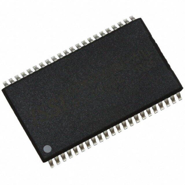
| 产品图片 |
|
| rohs | 符合RoHS无铅 / 符合限制有害物质指令(RoHS)规范要求 |
| 产品系列 | 内存,闪存,Microchip Technology SST25VF064C-80-4C-Q2AESST25 |
| 数据手册 | http://www.microchip.com/mymicrochip/filehandler.aspx?ddocname=en550510http://www.microchip.com/mymicrochip/filehandler.aspx?ddocname=en556157 |
| 产品型号 | SST25VF064C-80-4C-Q2AE |
| 产品种类 | 闪存 |
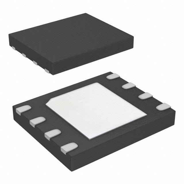
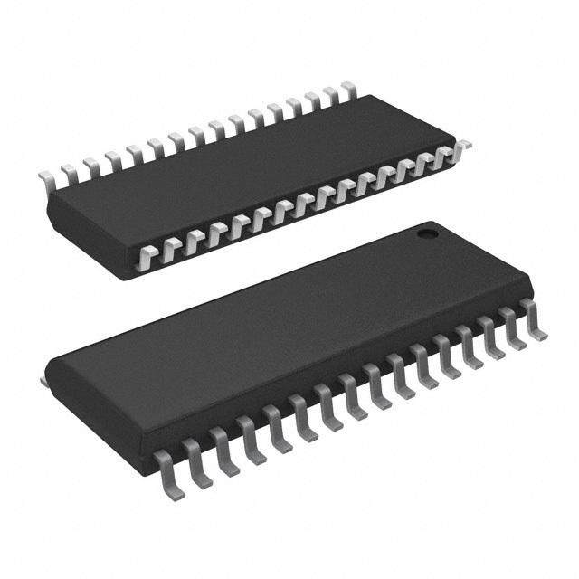
| 供应商器件封装 | 8-WSON |
| 包装 | 托盘 |
| 商标 | Microchip Technology |
| 存储器类型 | FLASH |
| 存储容量 | 64 Mbit |
| 存储类型 | NOR |
| 安装风格 | SMD/SMT |
| 定时类型 | Synchronous |
| 封装 | Tray |
| 封装/外壳 | 8-WDFN 裸露焊盘 |
| 封装/箱体 | WSON-8 |
| 工作温度 | 0 C to + 70 C |
| 工作温度范围 | 0 C to + 70 C |
| 工厂包装数量 | 480 |
| 接口 | SPI 串行 |
| 接口类型 | SPI |
| 数据总线宽度 | 8 bit |
| 最大工作电流 | 25 mA |
| 最大时钟频率 | 80 MHz |
| 标准包装 | 480 |
| 格式-存储器 | 闪存 |
| 电压-电源 | 2.7 V ~ 3.6 V |
| 电源电压-最大 | 3.6 V |
| 电源电压-最小 | 2.7 V |
| 系列 | SST25VF |
| 组织 | 8 M x 8 |
| 结构 | Sector |
| 访问时间 | 80 ns |
| 速度 | 80 MHz |


/IS61LPS102418B-200B3LI.jpg)

- 商务部:美国ITC正式对集成电路等产品启动337调查
- 曝三星4nm工艺存在良率问题 高通将骁龙8 Gen1或转产台积电
- 太阳诱电将投资9.5亿元在常州建新厂生产MLCC 预计2023年完工
- 英特尔发布欧洲新工厂建设计划 深化IDM 2.0 战略
- 台积电先进制程称霸业界 有大客户加持明年业绩稳了
- 达到5530亿美元!SIA预计今年全球半导体销售额将创下新高
- 英特尔拟将自动驾驶子公司Mobileye上市 估值或超500亿美元
- 三星加码芯片和SET,合并消费电子和移动部门,撤换高东真等 CEO
- 三星电子宣布重大人事变动 还合并消费电子和移动部门
- 海关总署:前11个月进口集成电路产品价值2.52万亿元 增长14.8%


PDF Datasheet 数据手册内容提取
Obsolete Device Please contact Microchip Sales for replacement information. 64 Mbit SPI Serial Dual I/O Flash SST25VF064C EOL Data Sheet The SST 25 series Serial Flash family features a four-wire, SPI-compatible inter- face that allows for a low pin-count package which occupies less board space and ultimately lowers total system costs. SST25VF064C SPI serial flash memory is manufactured with SST proprietary, high-performance CMOS SuperFlash tech- nology. The split-gate cell design and thick-oxide tunneling injector attain better reliability and manufacturability compared with alternate approaches. Features • Single Voltage Read and Write Operations (cid:129) Page-Program –2.7-3.6V –256 Bytes per page –Single and Dual Input support (cid:129) Serial Interface Architecture –Fast Page-Program time in 1.5 ms (typical) –SPI Compatible: Mode 0 and Mode 3 (cid:129) End-of-Write Detection (cid:129) Dual Input/Output Support –Software polling the BUSY bit in Status Register –Fast-Read Dual-Output Instruction (cid:129) Write Protection (WP#) –Fast-Read Dual I/O Instruction –Enables/Disables the Lock-Down function of the (cid:129) High Speed Clock Frequency status register –80 MHz for High-Speed Read (0BH) (cid:129) Software Write Protection –75 MHz for Fast-Read Dual-Output (3BH) –50 MHz for Fast-Read Dual I/O (BBH) –Write protection through Block-Protection bits in status –33 MHz for Read Instruction (03H) register (cid:129) Superior Reliability (cid:129) Security ID –Endurance: 100,000 Cycles (typical) –One-Time Programmable (OTP) 256 bit, Secure ID –Greater than 100 years Data Retention -64 bit Unique, Factory Pre-Programmed identifier -192 bit User-Programmable (cid:129) Low Power Consumption (cid:129) Temperature Range –Active Read Current: 12 mA (typical @ 80 MHz) for sin- gle-bit read) –Commercial = 0°C to +70°C –Active Read Current: 14 mA (typical @ 75MHz) for dual- –Industrial: -40°C to +85°C bit read) –Standby Current: 5 µA (typical) (cid:129) Packages Available –16-lead SOIC (300 mils) (cid:129) Flexible Erase Capability –8-contact WSON (6mm x 8mm) –Uniform 4 KByte sectors –8-lead SOIC (200 mils) –Uniform 32 KByte overlay blocks –Uniform 64 KByte overlay blocks (cid:129) All devices are RoHS compliant (cid:129) Fast Erase –Chip-Erase Time: 35 ms (typical) –Sector-/Block-Erase Time: 18 ms (typical) www.microchip.com ©2015 Silicon Storage Technology, Inc. DS20005036C 04/15
64 Mbit SPI Serial Dual I/O Flash SST25VF064C EOL Data Sheet Product Description The SST 25 series Serial Flash family features a four-wire, SPI-compatible interface that allows for a low pin-count package which occupies less board space and ultimately lowers total system costs. SST25VF064C SPI serial flash memory is manufactured with SST proprietary, high-performance CMOS SuperFlash technology. The split-gate cell design and thick-oxide tunneling injector attain bet- ter reliability and manufacturability compared with alternate approaches. The SST25VF064C significantly improves performance and reliability, while lowering power consump- tion. The device writes (Program or Erase) with a single power supply of 2.7-3.6V. The total energy consumed is a function of the applied voltage, current, and time of application. Since for any given volt- age range, the SuperFlash technology uses less current to program and has a shorter erase time, the total energy consumed during any Erase or Program operation is less than alternative flash memory technologies. The SST25VF064C device is offered in 16-lead SOIC (300 mils), 8-contact WSON (6mm x 8mm), and 8-lead SOIC (200 mils) packages. See Figure 2 for pin assignments. ©2015 Silicon Storage Technology, Inc. DS20005036C 04/15 2
64 Mbit SPI Serial Dual I/O Flash SST25VF064C EOL Data Sheet Block Diagram SuperFlash X - Decoder Address Memory Buffers and Latches Y - Decoder Page Buffer, I/O Buffers Control Logic and Data Latches Serial Interface CE# SCK SI/SIO0 SO/SIO1 WP# RST#/HOLD# 1392 B1.0 Figure 1: Functional Block Diagram ©2015 Silicon Storage Technology, Inc. DS20005036C 04/15 3
64 Mbit SPI Serial Dual I/O Flash SST25VF064C EOL Data Sheet Pin Description RST#/HOLD# SCK VDD SI/SIO0 CE# 1 8 VDD NC Top View NC SO/SIO1 2 Top View 7 RST#/HOLD# WP# 3 6 SCK NC NC NC NC VSS 4 5 SI/SIO0 NC NC CE# VSS 1392 8-WSON P1.0 SO/SIO1 WP# 1392 16-SOIC P1.0 CE# 1 8 VDD SO/SIO1 2 7 RST#/HOLD# Top View WP# 3 6 SCK VSS 4 5 SI/SIO0 1392 8-soic S3A P3.1 Figure 2: Pin Assignments for 16-Lead SOIC, 8-Contact WSON, and 8-Lead SOIC Table 1: Pin Description Symbol Pin Name Functions SCK Serial Clock To provide the timing of the serial interface. Commands, addresses, or input data are latched on the rising edge of the clock input, while output data is shifted out on the falling edge of the clock input. SI Serial Data Input To transfer commands, addresses, or data serially into the device. Inputs are latched on the rising edge of the serial clock. SO Serial Data Output To transfer data serially out of the device. Data is shifted out on the falling edge of the serial clock. SIO[0:1] Serial Data Input/ To transfer commands, addresses, or data serially into the device, or data Output for Dual I/ out of the device. Inputs are latched on the rising edge of the serial clock. O Mode Data is shifted out on the falling edge of the serial clock. These pins are for Dual I/O mode. CE# Chip Enable The device is enabled by a high to low transition on CE#. CE# must remain low for the duration of any command sequence. WP# Write Protect The Write Protect (WP#) pin is used to enable/disable BPL bit in the status register. RST#/HOLD# Reset To reset the operation of the device and the internal logic. The device pow- ers on with RST# pin functionality as default. Hold To temporarily stop serial communication with SPI Flash memory while device is selected. This is selected by an instruction sequence. See “Reset/ Hold Mode” page 5 for details. V Power Supply To provide power supply voltage: 2.7-3.6V DD V Ground SS T1.0 25036 ©2015 Silicon Storage Technology, Inc. DS20005036C 04/15 4
64 Mbit SPI Serial Dual I/O Flash SST25VF064C EOL Data Sheet Memory Organization The SST25VF064C SuperFlash memory array is organized in uniform 4 KByte erasable sectors with 32 KByte overlay blocks and 64 KByte overlay erasable blocks. Device Operation The SST25VF064C is accessed through the SPI (Serial Peripheral Interface) bus compatible protocol. The SPI bus consists of four control lines; Chip Enable (CE#) is used to select the device, and data is accessed through the Serial Data Input (SI), Serial Data Output (SO), and Serial Clock (SCK). The SST25VF064C supports both Mode 0 (0,0) and Mode 3 (1,1) of SPI bus operations. The difference between the two modes, as shown in Figure 3, is the state of the SCK signal when the bus master is in Stand-by mode and no data is being transferred. The SCK signal is low for Mode 0 and SCK signal is high for Mode 3. For both modes, the Serial Data In (SI) is sampled at the rising edge of the SCK clock signal and the Serial Data Output (SO) is driven after the falling edge of the SCK clock signal. CE# MODE 3 MODE 3 SCK MODE 0 MODE 0 SI Bit 7 Bit 6 Bit 5 Bit 4 Bit 3 Bit 2 Bit 1 Bit 0 DON'T CARE MSB HIGH IMPEDANCE SO Bit 7 Bit 6 Bit 5 Bit 4 Bit 3 Bit 2 Bit 1 Bit 0 MSB 1392 F04.0 Figure 3: SPI Protocol Reset/Hold Mode The RST#/HOLD# pin provides either a hardware reset or a hold pin. From power-on, the RST#/ HOLD# pin defaults as a hardware reset pin (RST#). The Hold mode for this pin is a user selected option where an EHLD instruction enables the Hold mode. Once selected as a hold pin (HOLD#), the RST#/HOLD# pin will be configured as a HOLD# pin, and goes back to RST# pin only after a power-off and power-on sequence. ©2015 Silicon Storage Technology, Inc. DS20005036C 04/15 5
64 Mbit SPI Serial Dual I/O Flash SST25VF064C EOL Data Sheet Reset If the RST#/HOLD# pin is used as a reset pin, RST# pin provides a hardware method for resetting the device. Driving the RST# pin high puts the device in normal operating mode. The RST# pin must be driven low for a minimum of T time to reset the device. The SO pin is in high impedance state while RST the device is in reset. A successful reset will reset the status register to its power-up state (BPL, BUSY and WEL = 0; BP3, BP2, BP1, and BP0 = 1). See Table 2 for default power-up modes. A device reset during an active Program or Erase operation aborts the operation and data of the targeted address range may be corrupted or lost due to the aborted erase or program operation. CE# TRECR TRECP TRECE SCK TRST RST# TRHZ SO SI 1292 F28.0 Figure 4: Reset Timing Diagram Table 2: Reset Timing Parameters Symbol Parameter Min Max Units T Reset Pulse Width 100 ns RST T Reset to High-Z Output 105 ns RHZ T Reset Recovery from Read 100 ns RECR T Reset Recovery from Program 10 µs RECP T Reset Recovery from Erase 1 ms RECE T2.25036 ©2015 Silicon Storage Technology, Inc. DS20005036C 04/15 6
64 Mbit SPI Serial Dual I/O Flash SST25VF064C EOL Data Sheet Hold Operation The EHLD instruction enables the hold pin functionality of the RST#/HOLD# pin. Once converted to a hold pin, the RST#/HOLD# pin functions as a hold pin until the device is powered off and on. After the power cycle, the pin functionality returns as a reset pin (RST#) after the power on. The HOLD# pin is used to pause a serial sequence using the SPI flash memory, but without resetting the clocking sequence. To activate the HOLD# mode, CE# must be in active low state. The HOLD# mode begins when the SCK active low state coincides with the falling edge of the HOLD# signal. The HOLD mode ends when the HOLD# signal’s rising edge coincides with the SCK active low state. If the falling edge of the HOLD# signal does not coincide with the SCK active low state, then the device enters Hold mode when the SCK next reaches the active low state. Similarly, if the rising edge of the HOLD# signal does not coincide with the SCK active low state, then the device exits from Hold mode when the SCK next reaches the active low state. See Figure 5 for Hold Condition waveform. Once the device enters Hold mode, SO will be in high-impedance state while SI and SCK can be V or V IL IH. If CE# is driven high during a Hold condition, the device returns to Standby mode. As long as HOLD# signal is low, the memory remains in the Hold condition. To resume communication with the device, HOLD# must be driven active high, and CE# must be driven active low. See Figure 5 for Hold timing. SCK HOLD# Active Hold Active Hold Active 1392 F05.0 Figure 5: Hold Condition Waveform Write Protection SST25VF064C provides software Write protection. The Write Protect pin (WP#) enables or disables the lock-down function of the status register. The Block-Protection bits (BP3, BP2, BP1, BP0, and BPL) in the status register provide Write protection to the memory array and the status register. See Table 5 for the Block-Protection description. Write Protect Pin (WP#) The Write Protect (WP#) pin enables the lock-down function of the BPL bit (bit 7) in the status register. When WP# is driven low, the execution of the Write-Status-Register (WRSR) instruction is determined by the value of the BPL bit (see Table 3). When WP# is high, the lock-down function of the BPL bit is disabled. Table 3: Conditions to execute Write-Status-Register (WRSR) Instruction WP# BPL Execute WRSR Instruction L 1 Not Allowed L 0 Allowed H X Allowed T3.0 25036 ©2015 Silicon Storage Technology, Inc. DS20005036C 04/15 7
64 Mbit SPI Serial Dual I/O Flash SST25VF064C EOL Data Sheet Security ID SST25VF064C offers a 256-bit Security ID (Sec ID) feature. The Security ID space is divided into two parts – one factory-programmed, 64-bit segment and one user-programmable 192-bit segment. The factory-programmed segment is programmed at SST with a unique number and cannot be changed. The user-programmable segment is left unprogrammed for the customer to program as desired. Use the Program SID command to program the Security ID using the address shown in Table 7. Once programmed, the Security ID can be locked using the Lockout SID command. This prevents any future write to the Security ID. The factory-programmed portion of the Security ID can never be programmed, and none of the Secu- rity ID can be erased. Status Register The software status register provides status on whether the flash memory array is available for any Read or Write operation, whether the device is Write enabled, and the state of the Memory Write pro- tection. During an internal Erase or Program operation, the status register may be read only to deter- mine the completion of an operation in progress. Table 4 describes the function of each bit in the software status register. Table 4: Status Register Default at Bit Name Function Power-up Read/Write 0 BUSY 1 = Internal Write operation is in progress 0 R 0 = No internal Write operation is in progress 1 WEL 1 = Device is memory Write enabled 0 R 0 = Device is not memory Write enabled 2 BP0 Indicate current level of block write protection (See Table 5) 1 R/W 3 BP1 Indicate current level of block write protection (See Table 5) 1 R/W 4 BP2 Indicate current level of block write protection (See Table 5) 1 R/W 5 BP3 Indicate current level of block write protection (See Table 5) 1 R/W 6 SEC1 Security ID status 01 R 1 = Security ID space locked 0 = Security ID space not locked 7 BPL 1 = BP3, BP2, BP1, BP0 are read-only bits 0 R/W 0 = BP3, BP2, BP1, BP0 are readable/writable T4.025036 1. The Security ID status will always be ‘1’ at power-up after a successful execution of the Lockout SID instruction; other- wise, the default at power up is ‘0’. ©2015 Silicon Storage Technology, Inc. DS20005036C 04/15 8
64 Mbit SPI Serial Dual I/O Flash SST25VF064C EOL Data Sheet Busy The Busy bit determines whether there is an internal Erase or Program operation in progress. A ‘1’ for the Busy bit indicates the device is busy with an operation in progress. A ‘0’ indicates the device is ready for the next valid operation. Write Enable Latch (WEL) The Write-Enable-Latch bit indicates the status of the internal memory Write Enable Latch. If the Write-Enable-Latch bit is set to ‘1’, it indicates the device is Write enabled. If the bit is set to ‘0’ (reset), it indicates the device is not Write enabled and does not accept any memory Write (Program/Erase) commands. The Write-Enable-Latch bit is automatically reset under the following conditions: (cid:129) Power-up (cid:129) Write-Disable (WRDI) instruction completion (cid:129) Write-Status Register instruction completion (cid:129) Page-Program instruction completion (cid:129) Dual-Input Page-Program instruction completion (cid:129) Sector-Erase instruction completion (cid:129) Block-Erase instruction completion (cid:129) Chip-Erase instruction completion (cid:129) Program SID instruction completion (cid:129) Lockout SID instruction completion Block Protection (BP3,BP2, BP1, BP0) The Block-Protection (BP3, BP2, BP1, BP0) bits define the size of the memory area, as shown in Table 5, to be software protected against any memory Write (Program or Erase) operation. The Write-Status- Register (WRSR) instruction is used to program the BP3, BP2, BP1 and BP0 bits as long as WP# is high or the Block-Protect-Lock (BPL) bit is 0. Chip-Erase can only be executed if Block-Protection bits are all 0. After power-up, BP3, BP2, BP1 and BP0 are set to the defaults specified in Table 5. Block Protection Lock-Down (BPL) WP# pin driven low (V ), enables the Block-Protection-Lock-Down (BPL) bit. When BPL is set to 1, it pre- IL vents any further alteration of the BPL, BP3, BP2, BP1, and BP0 bits. When the WP# pin is driven high (V ), the BPL bit has no effect and its value is “Don’t Care”. After power-up, the BPL bit is reset to 0. IH ©2015 Silicon Storage Technology, Inc. DS20005036C 04/15 9
64 Mbit SPI Serial Dual I/O Flash SST25VF064C EOL Data Sheet Security ID Status (SEC) The Security ID Status (SEC) bit indicates when the Security ID space is locked to prevent a Write command. The SEC is ‘1’ after the host issues a Lockout SID command. Once the host issues a Lock- out SID command, the SEC bit can never be reset to ‘0.’ Table 5: Software Status Register Block Protection FOR SST25VF064C Status Register Bit1 Protected Memory Address Protection Level BP3 BP2 BP1 BP0 64 Mbit None 0 0 0 0 None Upper 1/128 0 0 0 1 7F0000H-7FFFFFH Upper 1/64 0 0 1 0 7E0000H-7FFFFFH Upper 1/32 0 0 1 1 7C0000H-7FFFFFH Upper 1/16 0 1 0 0 780000H-7FFFFFH Upper 1/8 0 1 0 1 700000H-7FFFFFH Upper 1/4 0 1 1 0 600000H-7FFFFFH Upper 1/2 0 1 1 1 400000H-7FFFFFH All Blocks 1 0 0 0 000000H-7FFFFFH All Blocks 1 0 0 1 000000H-7FFFFFH All Blocks 1 0 1 0 000000H-7FFFFFH All Blocks 1 0 1 1 000000H-7FFFFFH All Blocks 1 1 0 0 000000H-7FFFFFH All Blocks 1 1 0 1 000000H-7FFFFFH All Blocks 1 1 1 0 000000H-7FFFFFH All Blocks 1 1 1 1 000000H-7FFFFFH T5.0 25036 1. Default at power-up for BP3, BP2, BP1, and BP0 is ‘1111’. (All Blocks Protected) ©2015 Silicon Storage Technology, Inc. DS20005036C 04/15 10
64 Mbit SPI Serial Dual I/O Flash SST25VF064C EOL Data Sheet Instructions Instructions are used to read, write (Erase and Program), and configure the SST25VF064C. The instruction bus cycles are 8 bits each for commands (Op Code), data, and addresses. The Write- Enable (WREN) instruction must be executed prior any Page-Program, Dual-Input Page-Program, Sector-Erase, Block-Erase, Write-Status-Register, Chip-Erase, Program SID, or Lockout SID instruc- tions. The complete list of instructions is provided in Table 6. All instructions are synchronized off a high to low transition of CE#. Inputs will be accepted on the ris- ing edge of SCK starting with the most significant bit. CE# must be driven low before an instruction is entered and must be driven high after the last bit of the instruction has been shifted in (except for Read, Read-ID, and Read-Status-Register instructions). Any low to high transition on CE#, before receiving the last bit of an instruction bus cycle, will terminate the instruction in progress and return the device to standby mode. Instruction commands (Op Code), addresses, and data are all input from the most significant bit (MSB) first. Table 6: Device Operation Instructions Address Dummy Data Instruction Description Op Code Cycle1 Cycle(s)2 Cycle(s) Cycle(s) Read Read Memory 0000 0011b (03H) 3 0 1 to Fast-Read Dual I/O Read Memory with Dual Address Input 1011 1011b (BBH) 33 13 1 to 3 and Data Output Fast-Read Dual-Out- Read Memory with Dual Output 0011 1011b (3BH) 3 1 1 to 3 put High-Speed Read Read Memory at Higher Speed 0000 1011b (0BH) 3 1 1 to Sector-Erase4 Erase 4 KByte of memory array 0010 0000b (20H) 3 0 0 32 KByte Block-Erase5 Erase 32KByte block of memory array 0101 0010b (52H) 3 0 0 64 KByte Block-Erase6 Erase 64 KByte block of memory array 1101 1000b (D8H) 3 0 0 Chip-Erase Erase Full Memory Array 0110 0000b (60H) or 0 0 0 1100 0111b (C7H) Page-Program To Program 1 to 256 Data Bytes 0000 0010b (02H) 3 0 1 to 256 Dual-Input Page- To Program 1 to 256 Data Bytes 1010 0010b (A2H) 3 0 1 to 1283 Program RDSR7 Read-Status-Register 0000 0101b (05H) 0 0 1 to EWSR Enable-Write-Status-Register 0101 0000b (50H) 0 0 0 WRSR Write-Status-Register 0000 0001b (01H) 0 0 1 WREN Write-Enable 0000 0110b (06H) 0 0 0 WRDI Write-Disable 0000 0100b (04H) 0 0 0 RDID8 Read-ID 1001 0000b (90H) or 3 0 1 to 1010 1011b (ABH) JEDEC-ID JEDEC ID Read 1001 1111b (9FH) 0 0 3 to EHLD Enable HOLD# pin functionality of the 1010 1010b (AAH) 0 0 0 RST#/HOLD# pin Read SID Read Security ID 1000 1000b (88H) 1 1 1 to 32 Program SID9 Program User Security ID area 1010 0101b (A5H) 1 0 1 to 24 Lockout SID9 Lockout Security ID Programming 1000 0101b (85H) 0 0 0 T6.0 25036 1. One bus cycle is eight clock periods. ©2015 Silicon Storage Technology, Inc. DS20005036C 04/15 11
64 Mbit SPI Serial Dual I/O Flash SST25VF064C EOL Data Sheet 2. Address bits above the most significant bit can be either VIL or VIH. 3. One bus cycle is four clock periods (dual operation) 4. 4KByte Sector Erase addresses: use AMS-A12, remaining addresses are don’t care but must be set either at VIL or VIH. 5. 32KByte Block Erase addresses: use AMS-A15, remaining addresses are don’t care but must be set either at VIL or VIH. 6. 64KByte Block Erase addresses: use AMS-A16, remaining addresses are don’t care but must be set either at VIL or VIH. 7. The Read-Status-Register is continuous with ongoing clock cycles until terminated by a low to high transition on CE#. 8. Manufacturer’s ID is read with A0 = 0, and Device ID is read with A0 = 1. All other address bits are 00H. The Manufac- turer’s ID and device ID output stream is continuous until terminated by a low-to-high transition on CE#. 9. Requires a prior WREN command. Read (33 MHz) The Read instruction, 03H, supports up to 33 MHz Read. The device outputs the data starting from the specified address location. The data output stream is continuous through all addresses until termi- nated by a low to high transition on CE#. The internal address pointer will automatically increment until the highest memory address is reached. Once the highest memory address is reached, the address pointer will automatically increment to the beginning (wrap-around) of the address space. For example, once the data from address location 7FFFFFH has been read, the next output will be from address location 000000H. The Read instruction is initiated by executing an 8-bit command, 03H, followed by address bits A -A . 23 0 CE# must remain active low for the duration of the Read cycle. See Figure 6 for the Read sequence. CE# MODE 3 0 1 2 3 4 5 6 7 8 1516 2324 3132 3940 47 48 5556 6364 70 SCK MODE 0 03 ADD. ADD. ADD. SI MSB MSB N N+1 N+2 N+3 N+4 HIGH IMPEDANCE SO DOUT DOUT DOUT DOUT DOUT MSB 1392 F06.0 Figure 6: Read Sequence ©2015 Silicon Storage Technology, Inc. DS20005036C 04/15 12
64 Mbit SPI Serial Dual I/O Flash SST25VF064C EOL Data Sheet High-Speed Read (80 MHz) The High-Speed Read instruction supporting up to 80 MHz Read is initiated by executing an 8-bit com- mand, 0BH, followed by address bits A -A and a dummy byte. CE# must remain active low for the 23 0 duration of the High-Speed Read cycle. See Figure 7 for the High-Speed Read sequence. Following a dummy cycle, the High-Speed Read instruction outputs the data starting from the specified address location. The data output stream is continuous through all addresses until terminated by a low to high transition on CE#. The internal address pointer will automatically increment until the highest memory address is reached. Once the highest memory address is reached, the address pointer will automatically increment to the beginning (wrap-around) of the address space. For example, once the data from address location 7FFFFFH is read, the next output is from address location 000000H. CE# MODE 3 0 1 2 3 4 5 6 7 8 1516 2324 3132 3940 4748 5556 6364 7172 80 SCK MODE 0 SI 0B ADD. ADD. ADD. X N N+1 N+2 N+3 N+4 HIGH IMPEDANCE SO DOUT DOUT DOUT DOUT DOUT MSB 1392 F07.0 Figure 7: High-Speed Read Sequence ©2015 Silicon Storage Technology, Inc. DS20005036C 04/15 13
64 Mbit SPI Serial Dual I/O Flash SST25VF064C EOL Data Sheet Fast-Read Dual-Output (75 MHz) The Fast-Read Dual-Output (3BH) instruction outputs data up to 75 MHz from the SIO and SIO pins. 0 1 To initiate the instruction, execute an 8-bit command (3BH) followed by address bits A23-A0 and a dummy byte on SI/SIO . Following a dummy cycle, the Fast-Read Dual-Output instruction outputs the 0 data starting from the specified address location on the SIO and SIO lines. SIO outputs, per clock 1 0 1 sequence, odd data bits D7, D5, D3, and D1; and SIO outputs even data bits D6, D4, D2, and D0. 0 CE# must remain active low for the duration of the Fast-Read Dual-Output instruction cycle. See Fig- ure 8 for the Fast-Read Dual-Output sequence. The data output stream is continuous through all addresses until terminated by a low-to-high transition on CE#. The internal address pointer will automatically increment until the highest memory address is reached. Once the highest memory address is reached, the address pointer automatically increments to the beginning (wraparound) of the address space. for 64 Mbit density, once the data from address location 7FFFFFH has been read the next output will be from address location 000000H. CE# MODE 3 0 1 2 3 4 5 6 7 8 1516 28293031323334353637383940414243444546474849505152535455 SCK MODE 0 24-Bit Address Dummy Cycle IO, Switches from Input to Output SIO0 3B ADD. ADD. ADD. X 6 4 2 0 6 4 2 0 6 4 2 0 6 4 2 0 DOUT DOUT DOUT DOUT SIO1 HIGH IMPEDANCE 7 5 3 1 7 5 3 1 7 5 3 1 7 5 3 1 MSB MSB MSB MSB N N+1 N+2 N+3 1392 F08.1 Figure 8: Fast-Read Dual Output Sequence ©2015 Silicon Storage Technology, Inc. DS20005036C 04/15 14
64 Mbit SPI Serial Dual I/O Flash SST25VF064C EOL Data Sheet Fast-Read Dual I/O (50 MHz) The Fast-Read Dual I/O (BBH) instruction reduces the total number of input clock cycles, which results in faster data access. The device is first selected by driving Chip Enable CE# low. Fast-Read Dual I/O is initiated by executing an 8-bit command (BBH) on SI/SIO , thereafter, the device accepts address 0 bits A23-A0 and a dummy byte on SI/SIO and SO/SIO . It offers the capability to input address bits 0 1 A23-A0 at a rate of two bits per clock. Odd address bits A23 through A1 are input on SIO and even 1 address bits A22 through A0 are input on SIO , alternately For example the most significant bit is input 0 first followed by A23/22, A21/A20, and so on. Each bit is latched at the same rising edge of the Serial Clock (SCK). The input data during the dummy clocks is “don’t care”. However, the SIO and SIO pin 0 1 must be in high-impedance prior to the falling edge of the first data output clock. Following a dummy cycle, the Fast-Read Dual I/O instruction outputs the data starting from the speci- fied address location on the SIO and SIO lines. SIO outputs, per clock sequence, odd data bits D7, 1 0 1 D5, D3, and D1; and SIO outputs even data bits D6, D4, D2, and D0 per clock edge. CE# must remain 0 active low for the duration of the Fast-Read Dual I/O instruction cycle. The data output stream is con- tinuous through all addresses until terminated by a low-to-high transition on CE#. The internal address pointer will automatically increment until the highest memory address is reached. Once the highest memory address is reached, the address pointer automatically increments to the beginning (wraparound) of the address space. For example, once the data from address location 7FFFFFH is read, the next output is from address location 000000H. See Figure 9 for the Fast-Read Dual I/o sequence. CE# MODE 3 0 1 2 3 4 5 6 7 8 9 101112131415161718192021222324252627282930313233343536373839 SCK MODE 0 Dummy Cycle IO, Switches from Input to Output SIO0 BB 6 4 2 0 6 4 2 0 6 4 2 0 X 6 4 2 0 6 4 2 0 6 4 2 0 6 4 2 0 6 DOUT DOUT DOUT DOUT SIO1 7 5 3 1 7 5 3 1 7 5 3 1 X 7 5 3 1 7 5 3 1 7 5 3 1 7 5 3 1 7 MSB MSB MSB MSB A23-16 A15-8 A7-0 N N+1 N+2 N+3 1392 F29.0 Figure 9: Fast-Read Dual I/O Sequence ©2015 Silicon Storage Technology, Inc. DS20005036C 04/15 15
64 Mbit SPI Serial Dual I/O Flash SST25VF064C EOL Data Sheet Page-Program The page-Program instruction programs up to 256 bytes of data in the memory. The selected page address must be in the erased state (FFH) before initiating the Page-Program operation. A Page-Pro- gram applied to a protected memory area will be ignored. Prior to the program operation, the Write-Enabled (WREN) instruction must be executed. CE# must remain active low for the duration of the Page-Program instruction. The Page-Program instruction is initiated by executing an 8-bit command, 02H, followed by address bits A23-A0. Following the address, at least one byte is needed for the data input. CE# must be driven high before the instruction is exe- cuted. The user may poll the Busy bit in the software status register or wait T for the completion of PP the internal self-timed Page-Program operation. See Figure 10 for the Page-Program sequence. For Page-Program, the memory range for SST25VF064C is set in 256 byte page boundaries. The device handles shifting of more than 256 bytes of data by keeping the last 256 bytes of data shifted as the correct data to be programmed. If the target address for the Page-Program instruction is not the beginning of the page boundary (A7-A0 are not all zero) and the number of data input exceeds or over- laps the end of the address of the page boundary, the excess data inputs will wrap around and will be programmed at the start of that target page. CE# MODE 3 0 1 2 3 4 5 6 7 8 1516 2324 3132 39 SCK MODE 0 SI 02 ADD. ADD. ADD. Data Byte 1 MSB LSB MSB LSB MSB LSB SO HIGH IMPEDANCE CE# 40 41 42 43 44 45 46 47 48 49 50 51 52 53 54 55 2072 2073 2074 2075 2076 2077 2078 2079 SCK SI Data Byte 2 Data Byte 3 Data Byte 256 MSB LSBMSB LSB MSB LSB SO HIGH IMPEDANCE 1392 F30.0 Figure 10:Page-Program Sequence ©2015 Silicon Storage Technology, Inc. DS20005036C 04/15 16
64 Mbit SPI Serial Dual I/O Flash SST25VF064C EOL Data Sheet Dual-Input Page-Program (50 MHz) Dual-Input Page-Program instruction A2H, doubles the data input transfer of normal Page-Program instruction and supports up to 50MHz. Data to be programmed is entered using two I/O pins, SIO and 1 SIO . Prior to the program operation the Write-Enable (WREN) instruction must be executed. The 0 Dual-Input Page-Program instruction is entered by driving CE# low, followed by the instruction code, A2H, three address bytes, and at least one data byte on serial data inputs SIO and SIO pins. CE# 1 0 must be driven low for the entire duration of the sequence. The Dual-Input Page-Program instruction programs up to 256 bytes of data in the memory. The selected page address must be in the erased state (FFH) before initiating the Page-Program operation. A Dual-Input Page-Program applied to a pro- tected memory area will be ignored. CE# must be driven high after the seventh and eight bit of the last data byte has been latched; other- wise, the dual input program instruction is not executed. Once CE# is driven high the instruction is exe- cuted and the user may poll the WEL and Busy bit of the software status register or wait TPP for the completion of the internal self-timed Page-Program operation. See Figure 10 for the Dual-Input-Page- Program sequence. For Dual-Input Page-Program, the memory range for the SST25VF064C is set in 256 byte page boundaries. The device handles shifting of more than 256 bytes of data by keeping the last 256 bytes of data shifted as the correct data to be programmed. If the target address for the Page-Program instruction is not the beginning of the page boundary (A7-A0 are not all zero) and the number of data input exceeds or overlaps the end of the address of the page boundary, the excess data inputs will wrap around and will be programmed at the start of that target page. CE# MODE 3 0 1 2 3 4 5 6 7 8 9 10 2829303132333435363728394041424344454647 1052 1053 1054 1055 SCK MODE 0 24-bit Address (1) SIO0 A2 232221 3 2 1 0 6 4 2 0 6 4 2 0 6 4 2 0 6 4 2 0 6 4 2 0 Data Byte 1 Data Byte 2 Data Byte 3 Data Byte 4 Data Byte 256 High Impedance SIO1 7 5 3 1 7 5 3 1 7 5 3 1 7 5 3 1 7 5 3 1 MSB MSB MSB MSB MSB 1392 F31.0 Figure 11:Dual-Input Page-Program ©2015 Silicon Storage Technology, Inc. DS20005036C 04/15 17
64 Mbit SPI Serial Dual I/O Flash SST25VF064C EOL Data Sheet Sector-Erase The Sector-Erase instruction clears all bits in the selected 4 KByte sector to FFH. A Sector-Erase instruction applied to a protected memory area will be ignored. Prior to any Write operation, the Write- Enable (WREN) instruction must be executed. CE# must remain active low for the duration of any com- mand sequence. The Sector-Erase instruction is initiated by executing an 8-bit command, 20H, fol- lowed by address bits A -A . Address bits A -A (A = Most Significant address) are used to 23 0 MS 12 MS determine the sector address (SA ), remaining address bits can be V or V CE# must be driven high X IL IH. before the instruction is executed. Poll the Busy bit in the software status register or wait T for the SE completion of the internal self-timed Sector-Erase cycle. See Figure 12 for the Sector-Erase sequence. CE# MODE 3 0 1 2 3 4 5 6 7 8 1516 2324 31 SCK MODE 0 20 ADD. ADD. ADD. SI MSB MSB SO HIGH IMPEDANCE 1392 F13.0 Figure 12:Sector-Erase Sequence ©2015 Silicon Storage Technology, Inc. DS20005036C 04/15 18
64 Mbit SPI Serial Dual I/O Flash SST25VF064C EOL Data Sheet 32-KByte and 64-KByte Block-Erase The 32-KByte Block-Erase instruction clears all bits in the selected 32 KByte block to FFH. A Block- Erase instruction applied to a protected memory area will be ignored. The 64-KByte Block-Erase instruc- tion clears all bits in the selected 64 KByte block to FFH. A Block-Erase instruction applied to a protected mem- ory area will be ignored. Prior to any Write operation, the Write-Enable (WREN) instruction must be executed. CE# must remain active low for the duration of any command sequence. The 32-KByte Block-Erase instruction is initiated by executing an 8-bit command, 52H, followed by address bits A -A . Address 23 0 bits A -A (A = Most Significant Address) are used to determine block address (BA ), remaining MS 15 MS X address bits can be V or V CE# must be driven high before the instruction is executed. The 64-KByte Block- IL IH. Erase instruction is initiated by executing an 8-bit command D8H, followed by address bits A -A . Address bits 23 0 A -A are used to determine block address (BA ), remaining address bits can be V or V CE# must be MS 15 X IL IH. driven high before the instruction is executed. Poll the Busy bit in the software status register or wait T for BE the completion of the internal self-timed 32-KByte Block-Erase or 64-KByte Block-Erase cycles. See Figure 13 for the 32-KByte Block-Erase sequence and Figure 14 for the 64-KByte Block-Erase sequence. CE# MODE 3 0 1 2 3 4 5 6 7 8 1516 2324 31 SCK MODE 0 52 ADDR ADDR ADDR SI MSB MSB SO HIGH IMPEDANCE 1392 F32.0 Figure 13:32-KByte Block-Erase Sequence CE# MODE 3 0 1 2 3 4 5 6 7 8 1516 2324 31 SCK MODE 0 D8 ADDR ADDR ADDR SI MSB MSB SO HIGH IMPEDANCE 1327 F33.0 Figure 14:64-KByte Block-Erase Sequence ©2015 Silicon Storage Technology, Inc. DS20005036C 04/15 19
64 Mbit SPI Serial Dual I/O Flash SST25VF064C EOL Data Sheet Chip-Erase The Chip-Erase instruction clears all bits in the device to FFH. A Chip-Erase instruction will be ignored if any of the memory area is protected. Prior to any Write operation, the Write-Enable (WREN) instruction must be executed. CE# must remain active low for the duration of the Chip-Erase instruction sequence. Initiate the Chip-Erase instruction by executing an 8-bit command, 60H or C7H. CE# must be driven high before the instruction is executed. Poll the Busy bit in the software status register or wait T for the comple- CE tion of the internal self-timed Chip-Erase cycle. See Figure 15 for the Chip-Erase sequence. CE# MODE 3 0 1 2 3 4 5 6 7 SCK MODE 0 SI 60 or C7 MSB SO HIGH IMPEDANCE 1392 F16.0 Figure 15:Chip-Erase Sequence Read Security ID To execute a Read SID operation, the host drives CE# low, sends the Read SID command cycle (88H), one address cycle, and then one dummy cycle. Each cycle is eight bits long, most significant bit first. After the dummy cycle, the device outputs data on the falling edge of the SCK signal, starting from the specified address location. The data output stream is continuous through all SID addresses until termi- nated by a low-to-high transition on CE#. The internal address pointer automatically increments until the last SID address is reached, then outputs wrap around until CE# goes high. Lockout Security ID The Lockout SID instruction prevents any future changes to the Security ID. Prior to the Lockout SID operation, the Write-Enable (WREN) instruction must be executed. To execute a Lockout SID, the host drives CE# low, sends the Lockout SID command cycle (85H), then drives CE# high. A cycle is 8 bits long, most significant bit first. The user may poll the BUSY bit in the software status register or waits T for the completion of the Lockout SID operation. PSID ©2015 Silicon Storage Technology, Inc. DS20005036C 04/15 20
64 Mbit SPI Serial Dual I/O Flash SST25VF064C EOL Data Sheet Program Security ID The Program SID instruction programs one to 24 bytes of data in the user-programmable, Security ID space. The device ignores a Program SID instruction pointing to an invalid or protected address, see Table 7. Prior to the program operation, execute WREN. To execute a Program SID operation, the host drives CE# low, sends the Program SID command cycle (A5H), one address cycle, the data to be programmed, then drives CE# high. The programmed data must be between 1 to 24 Bytes and in whole Byte increments. To determine the completion of the inter- nal, self-timed Program SID operation, poll the BUSY bit in the software status register, or wait T PSID for the completion of the internal self-timed Program SID operation. Table 7: Program Security ID Program Security ID Address Range Pre-Programmed at factory 00H – 07H User Programmable 08H – 1FH T7.0 25036 Read-Status-Register (RDSR) The Read-Status-Register (RDSR) instruction allows reading of the status register. The status register may be read at any time even during a Write (Program/Erase) operation. When a Write operation is in progress, the Busy bit may be checked before sending any new commands to assure that the new commands are properly received by the device. CE# must be driven low before the RDSR instruction is entered and remain low until the status data is read. Read-Status-Register is continuous with ongoing clock cycles until it is terminated by a low to high transition of the CE#. See Figure 16 for the RDSR instruction sequence. CE# MODE 3 0 1 2 3 4 5 6 7 8 9 10 11 12 13 14 SCK MODE 0 SI 05 MSB HIGH IMPEDANCE SO Bit 7 Bit 6 Bit 5 Bit 4 Bit 3 Bit 2 Bit 1 Bit 0 MSB Status Register Out 1392 F17.0 Figure 16:Read-Status-Register (RDSR) Sequence ©2015 Silicon Storage Technology, Inc. DS20005036C 04/15 21
64 Mbit SPI Serial Dual I/O Flash SST25VF064C EOL Data Sheet Write-Enable (WREN) The Write-Enable (WREN) instruction sets the Write-Enable-Latch bit in the Status Register to ‘1’ allowing Write operations to occur. The WREN instruction must be executed prior to any Write (Pro- gram/Erase) operation. The WREN instruction may also be used to allow execution of the Write-Sta- tus-Register (WRSR) instruction; however, the Write-Enable-Latch bit in the Status Register will be cleared upon the rising edge CE# of the WRSR instruction. CE# must be driven high before the WREN instruction is executed. CE# MODE 3 0 1 2 3 4 5 6 7 SCK MODE 0 SI 06 MSB SO HIGH IMPEDANCE 1392 F18.0 Figure 17:Write Enable (WREN) Sequence Write-Disable (WRDI) The Write-Disable (WRDI) instruction resets the Write-Enable-Latch bit to ‘0,’ thereby, preventing any new Write operations. The WRDI instruction will not terminate any program or erase operation in prog- ress. Any program or erase operation in progress will continue after executing the WRDI instruction. CE# must be driven high before the WRDI instruction is executed. CE# MODE 3 0 1 2 3 4 5 6 7 SCK MODE 0 SI 04 MSB SO HIGH IMPEDANCE 1392 F19.0 Figure 18:Write Disable (WRDI) Sequence ©2015 Silicon Storage Technology, Inc. DS20005036C 04/15 22
64 Mbit SPI Serial Dual I/O Flash SST25VF064C EOL Data Sheet Enable-Write-Status-Register (EWSR) The Enable-Write-Status-Register (EWSR) instruction arms the Write-Status-Register (WRSR) instruction and opens the status register for alteration. The Write-Status-Register instruction must be executed immediately after the execution of the Enable-Write-Status-Register instruction. This two- step instruction sequence of the EWSR instruction followed by the WRSR instruction works like soft- ware data protection (SDP) command structure which prevents any accidental alteration of the status register values. CE# must be driven low before the EWSR instruction is entered and must be driven high before the EWSR instruction is executed. Write-Status-Register (WRSR) The Write-Status-Register instruction writes new values to the BP3, BP2, BP1, BP0, and BPL bits of the status register. CE# must be driven low before the command sequence of the WRSR instruction is entered and driven high before the WRSR instruction is executed. See Figure 19 for EWSR or WREN and WRSR instruction sequences. Executing the Write-Status-Register instruction will be ignored when WP# is low and BPL bit is set to ‘1’. When the WP# is low, the BPL bit can only be set from ‘0’ to ‘1’ to lock-down the status register, but cannot be reset from ‘1’ to ‘0’. When WP# is high, the lock-down function of the BPL bit is disabled and the BPL, BP0, BP1, BP2, and BP3 bits in the status register can all be changed. As long as BPL bit is set to ‘0’ or WP# pin is driven high (V ) prior to the low-to-high transition of the CE# pin at the end of IH the WRSR instruction, the bits in the status register can all be altered by the WRSR instruction. In this case, a single WRSR instruction can set the BPL bit to ‘1’ to lock down the status register as well as altering the BP0, BP1, BP2, and BP3 bits at the same time. See Table 3 for a summary description of WP# and BPL functions. CE# MODE 3 0 1 2 3 4 5 6 7 MODE 3 0 1 2 3 4 5 6 7 8 9 101112131415 SCK MODE 0 MODE 0 STATUS REGISTER IN SI 50 or 06 01 7 6 5 4 3 2 1 0 MSB MSB MSB HIGH IMPEDANCE SO 1392 F20.0 Figure 19:Enable-Write-Status-Register (EWSR) or Write-Enable (WREN) and Write-Sta- tus-Register (WRSR) Sequence ©2015 Silicon Storage Technology, Inc. DS20005036C 04/15 23
64 Mbit SPI Serial Dual I/O Flash SST25VF064C EOL Data Sheet Enable-Hold (EHLD) The 8-bit command, AAH, Enable-Hold instruction enables the HOLD functionality of the RST#/ HOLD# pin. CE# must remain active low for the duration of the Enable-Hold instruction sequence. CE# must be driven high before the instruction is executed. See Figure 20 for the Enable-Hold instruction sequence. CE# MODE 3 0 1 2 3 4 5 6 7 SCK MODE 0 SI AA MSB SO HIGH IMPEDANCE 1203 F21.0 Figure 20:Enable-Hold Sequence Read-ID (RDID) The Read-ID instruction (RDID) identifies the device as SST25VF064C and manufacturer as SST. The device information can be read from executing an 8-bit command, 90H or ABH, followed by address bits A -A . Following the Read-ID instruction, the manufacturer’s ID is located in address 00000H and 23 0 the device ID is located in address 00001H. Once the device is in Read-ID mode, the manufacturer’s and device ID output data toggles between address 00000H and 00001H until terminated by a low to high transition on CE#. After CE# is driven high, the device is put into standby mode. Refer to Tables 8 and 9 for device identification data. CE# MODE 3 0 1 2 3 4 5 6 7 8 1516 2324 3132 3940 4748 5556 63 SCK MODE 0 SI 90 or AB 00 00 ADD1 MSB MSB HIGH HIGH IMPEDANCE IMPEDANCE SO BF Device ID BF Device ID MSB Note: The manufacturer's and device ID output stream is continuous until terminated by a low to high transition on CE#. 1. 00H will output the manfacturer's ID first and 01H will output device ID first before toggling between the two. 1392 F21.0 Figure 21:Read-ID Sequence ©2015 Silicon Storage Technology, Inc. DS20005036C 04/15 24
64 Mbit SPI Serial Dual I/O Flash SST25VF064C EOL Data Sheet Table 8: Product Identification Address Data Manufacturer’s ID 00000H BFH Device ID SST25VF064C 00001H 4BH T8.025036 ©2015 Silicon Storage Technology, Inc. DS20005036C 04/15 25
64 Mbit SPI Serial Dual I/O Flash SST25VF064C EOL Data Sheet JEDEC Read-ID The JEDEC Read-ID instruction identifies the device as SST25VF064C and the manufacturer as SST. The device information can be read from executing the 8-bit command, 9FH. Following the JEDEC Read-ID instruction, the 8-bit manufacturer’s ID, BFH, is output from the device. After that, a 24-bit device ID is shifted out on the SO pin. Byte 1, BFH, identifies the manufacturer as SST. Byte 2, 25H, identifies the memory type as SPI Serial Flash. Byte 3, 4BH, identifies the device as SST25VF064C. The instruction sequence is shown in Figure 22. The JEDEC Read ID instruction is terminated by a low to high transition on CE# at any time during data output. CE# MODE 3 0 1 2 3 4 5 6 7 8 9 10111213141516171819202122232425262728293031 SCK MODE 0 SI 9F HIGH IMPEDANCE SO BF 25 4B MSB MSB 1392 F22.0 Figure 22:JEDEC Read-ID Sequence Table 9: JEDEC Read-ID Data Manufacturer’s ID Device ID Memory Type Memory Capacity Byte1 Byte 2 Byte 3 BFH 25H 4BH T9.0 25036 ©2015 Silicon Storage Technology, Inc. DS20005036C 04/15 26
64 Mbit SPI Serial Dual I/O Flash SST25VF064C EOL Data Sheet Electrical Specifications Absolute Maximum Stress Ratings Applied conditions greater than those listed under “Absolute Maximum Stress Ratings” may cause permanent damage to the device. This is a stress rating only and functional operation of the device at these conditions or conditions greater than those defined in the operational sections of this data sheet is not implied. Exposure to absolute maximum stress rating con- ditions may affect device reliability. Temperature Under Bias . . . . . . . . . . . . . . . . . . . . . . . . . . . . . . . . . . . . . . . . . . . . . . -55°C to +125°C Storage Temperature. . . . . . . . . . . . . . . . . . . . . . . . . . . . . . . . . . . . . . . . . . . . . . . . . -65°C to +150°C D. C. Voltage on Any Pin to Ground Potential . . . . . . . . . . . . . . . . . . . . . . . . . . . . .-0.5V to V +0.5V DD Transient Voltage (<20 ns) on Any Pin to Ground Potential. . . . . . . . . . . . . . . . . . .-2.0V to V +2.0V DD Package Power Dissipation Capability (T = 25°C). . . . . . . . . . . . . . . . . . . . . . . . . . . . . . . . . . . 1.0W A Surface Mount Solder Reflow Temperature. . . . . . . . . . . . . . . . . . . . . . . . . . . . 260°C for 10 seconds Output Short Circuit Current1. . . . . . . . . . . . . . . . . . . . . . . . . . . . . . . . . . . . . . . . . . . . . . . . . . . 50 mA 1. Output shorted for no more than one second. No more than one output shorted at a time. Table 10:Operating Range Range Ambient Temp V DD Commercial 0°C to +70°C 2.7-3.6V Industrial -40°C to +85°C 2.7-3.6V T10.1 25036 Table 11:AC Conditions of Test1 Input Rise/Fall Time Output Load 5ns C = 30 pF L T11.1 25036 1. See Figure 28 ©2015 Silicon Storage Technology, Inc. DS20005036C 04/15 27
64 Mbit SPI Serial Dual I/O Flash SST25VF064C EOL Data Sheet Table 12:DC Operating Characteristics (VDD = 2.7-3.6V) Limits Symbol Parameter Min Max Units Test Conditions I Read Current 12 mA CE# = 0.1 V /0.9 V @33 MHz, SO = open DDR DD DD I High-Speed Read Current 25 mA CE# = 0.1 V /0.9 V @80 MHz, SO = open DDR2 DD DD I Fast-Read Dual-Output/Dual I/ 25 mA CE# = 0.1 V /0.9 V @75/50 MHz DDR3 DD DD O Current I Program and Erase Current 25 mA CE# = V DDW DD I Standby Current 20 µA CE# = V , V = V or V SB1 DD IN DD SS I Input Leakage Current 1 µA V = GND to V , V = V Max LI IN DD DD DD I Output Leakage Current 1 µA V = GND to V , V = V Max LO OUT DD DD DD V Input Low Voltage 0.8 V V = V Min IL DD DD V Input High Voltage 0.7 V V V = V Max IH DD DD DD V Output Low Voltage 0.2 V I = 100 µA, V = V Min OL OL DD DD V Output High Voltage V -0.2 V I = -100 µA, V = V Min OH DD OH DD DD T12.025036 Table 13:Capacitance (TA = 25°C, f = 1 Mhz, other pins open) Parameter Description Test Condition Maximum C 1 Output Pin Capacitance V = 0V 12 pF OUT OUT C 1 Input Capacitance V = 0V 6 pF IN IN T13.025036 1. This parameter is measured only for initial qualification and after a design or process change that could affect this parameter. Table 14:Reliability Characteristics Symbol Parameter Minimum Specification Units Test Method N 1 Endurance 10,000 Cycles JEDEC Standard A117 END T 1 Data Retention 100 Years JEDEC Standard A103 DR I 1 Latch Up 100 + I mA JEDEC Standard 78 LTH DD T14.025036 1. This parameter is measured only for initial qualification and after a design or process change that could affect this parameter. ©2015 Silicon Storage Technology, Inc. DS20005036C 04/15 28
64 Mbit SPI Serial Dual I/O Flash SST25VF064C EOL Data Sheet Table 15:AC Operating Characteristics 33 MHz 50 MHz 75/80 MHz Symbol Parameter Min Max Min Max Min Max Units F 1 Serial Clock Frequency High-Speed Read 33 50 75/80 MHz CLK T Serial Clock High Time 13 9 6 ns SCKH T Serial Clock Low Time 13 9 6 ns SCKL T 2 Serial Clock Rise Time (Slew Rate) 0.1 0.1 0.1 V/ns SCKR T Serial Clock Fall Time (Slew Rate) 0.1 0.1 0.1 V/ns SCKF T 3 CE# Active Setup Time 5 5 5 ns CES T 3 CE# Active Hold Time 5 5 5 ns CEH T 3 CE# Not Active Setup Time 5 5 5 ns CHS T 3 CE# Not Active Hold Time 5 5 5 ns CHH T CE# High Time 50 50 50 ns CPH T 4 CE# High to High-Z Output 7 7 7 ns CHZ T SCK Low to Low-Z Output 0 0 0 ns CLZ T Data In Setup Time 3 3 2 ns DS T Data In Hold Time 5 5 4 ns DH T HOLD# Low Setup Time 5 5 5 ns HLS T HOLD# High Setup Time 5 5 5 ns HHS T HOLD# Low Hold Time 5 5 5 ns HLH T HOLD# High Hold Time 5 5 5 ns HHH T 4 HOLD# Low to High-Z Output 7 7 7 ns HZ T 4 HOLD# High to Low-Z Output 7 7 7 ns LZ T Output Hold from SCK Change 0 0 0 ns OH T Output Valid from SCK 15 10 6 ns V T Sector-Erase 25 25 25 ms SE T Block-Erase 25 25 25 ms BE T Chip-Erase 50 50 50 ms SCE T Page-Program 2.5 2.5 2.5 ms PP T Program Security ID 1.0 1.0 1.0 ms PSID T15.1 25036 1. Maximum clock frequency for Read Instruction, 03H, is 33 MHz Maximum clock frequency Fast-Read Dual-Output (3BH) is 75 MHz Maximum clock frequency Fast-Read Dual I/O (BBH) is 50 MHz Maximum clock frequency for High-Speed Read, OBH, is 80 MHz Maximum clock frequency for Dual-Input Page-Program, A2H, is 50 Mhz 2. Maximum Rise and Fall time may be limited by TSCKH and TSCKL requirements 3. Relative to SCK. 4. Not 100% tested in production. ©2015 Silicon Storage Technology, Inc. DS20005036C 04/15 29
64 Mbit SPI Serial Dual I/O Flash SST25VF064C EOL Data Sheet TCPH CE# TCHH TCES TCEH TCHS SCK TDS TDH TSCKR TSCKF SI MSB LSB HIGH-Z HIGH-Z SO 1392 F23.0 Figure 23:Serial Input Timing Diagram CE# TSCKH TSCKL SCK TOH TCLZ TCHZ SO MSB LSB TV SI 1392 F24.0 Figure 24:Serial Output Timing Diagram CE# THHH THLS THHS SCK THLH THZ TLZ SO SI HOLD# 1392 F25.0 Figure 25:Hold Timing Diagram ©2015 Silicon Storage Technology, Inc. DS20005036C 04/15 30
64 Mbit SPI Serial Dual I/O Flash SST25VF064C EOL Data Sheet Power-Up Specifications All functionalities and DC specifications are specified for a V ramp rate of greater than 1V per 100 DD ms (0V to 3V in less than 300 ms). If the VDD ramp rate is slower than 1V/100 ms, a hardware reset is required. The recommended V power-up to RESET# high time should be greater than 100 µs to DD ensure a proper reset. See Table 16 and Figures 26 and 27 for more information. Table 16:Recommended System Power-up Timings Symbol Parameter Minimum Units T 1 V Min to Read Operation 100 µs PU-READ DD T 1 V Min to Write Operation 100 µs PU-WRITE DD T16.025036 1. This parameter is measured only for initial qualification and after a design or process change that could affect this parameter. TPU-READ VDD VDD min 0V RESET# VIH TRECR CE# Note: See Table2 1292 F36.0 Figure 26:Power-Up Reset Diagram VDD VDD Max Chip selection is not allowed. All commands are rejected by the device. VDD Min TPU-READ Device fully accessible TPU-WRITE Time 1392 F26.0 Figure 27:Power-up Timing Diagram ©2015 Silicon Storage Technology, Inc. DS20005036C 04/15 31
64 Mbit SPI Serial Dual I/O Flash SST25VF064C EOL Data Sheet VIHT VHT VHT INPUT REFERENCE POINTS OUTPUT VLT VLT VILT 1392 F37.0 AC test inputs are driven at V (0.9V ) for a logic “1” and V (0.1V ) for a logic “0”. IHT DD ILT DD Measurement reference points for inputs and outputs are V (0.6V ) and V (0.4V ). HT DD LT DD Input rise and fall times (10% 90%) are <5 ns. Note: VHT - VHIGH Test VLT - VLOW Test VIHT - VINPUT HIGH Test VILT - VINPUT LOW Test Figure 28:AC Input/Output Reference Waveforms ©2015 Silicon Storage Technology, Inc. DS20005036C 04/15 32
64 Mbit SPI Serial Dual I/O Flash SST25VF064C EOL Data Sheet Product Ordering Information SST 25 VF 064C - 80 - 4I - SAE XX XX XXXX - XX - XX - XXX Environmental Attribute E1 = non-Pb Package Modifier C = 16 leads A = 8 contacts Package Type S = SOIC (300 mil body width) Q2 = WSON (6mm x 8mm) S3 = SOIC (200 mil body width) Temperature Range C = Commercial = 0°C to +70°C I = Industrial = -40°C to +85°C Minimum Endurance 4 = 10,000 cycles Operating Frequency 80 = 80 MHz Version C = Page-Program Device Density 064 = 64 Mbit Voltage V = 2.7-3.6V Product Series 25 = Serial Peripheral Interface flash memory 1. Environmental suffix “E” denotes non-Pb sol- der. SST non-Pb solder devices are “RoHS Compliant”. Valid combinations for SST25VF064C SST25VF064C-80-4I-SCE SST25VF064C-80-4I-S3AE SST25VF064C-80-4I-Q2AE SST25VF064C-80-4C-Q2AE Note:Valid combinations are those products in mass production or will be in mass production. Consult your SST sales representative to confirm availability of valid combinations and to determine availability of new combi- nations. ©2015 Silicon Storage Technology, Inc. DS20005036C 04/15 33
64 Mbit SPI Serial Dual I/O Flash SST25VF064C EOL Data Sheet Packaging Diagrams 7.40 10.00 7.60 10.65 Pin #1 Identifier 10.08 † 10.50 7° .020x45° 7° 4 places 4 places 2.35 2.65 .33 .10 .23 .51 1.27 BSC .30 .32 .38 ‡ 1.27 16.soic-SC-ILL.3 Note: 1. Complies with JEDEC publication 95 MS-013 AA dimensions (except as noted), although some dimensions may be more stringent. † = JEDEC min is 10.10; SST min (10.08) is less stringent ‡ = JEDEC min is 0.40; SST min (0.38) is less stringent 2. All linear dimensions are in metric (min/max). 3. Coplanarity: 0.1 (±.05) mm. 4. Maximum allowable mold flash is 0.15mm at the package ends, and 0.25mm between leads. Figure 29:16-Lead Plastic Small Outline Integrated Circuit (SOIC) SST Package Code SC ©2015 Silicon Storage Technology, Inc. DS20005036C 04/15 34
64 Mbit SPI Serial Dual I/O Flash SST25VF064C EOL Data Sheet TOP VIEW SIDE VIEW BOTTOM VIEW 8.00 0.2 ±0.10 Pin Pin #1 #1 1.27 BSC 6 7 0 6.00 0. 4.8 ±0.10 0.45 0.35 6.0 A A 0.55 0.05 0.45 Max 0.80 CROSS SECTION 0.70 Detail A-A Note: 1. All linear dimensions are in millimeters (max/min). 2. Untoleranced dimensions are nominal target dimensions. 0.80 3. The external paddle is electrically connected to die back-side and VSS. 0.70 This paddle can be soldered to the PC board; SST suggests connecting this paddle to VSS of the unit. Connection of this paddle to any other voltage potential will result in shorts and/or electrical malfunction of the device. 1mm 8-wson-6x8-Q2A-2.0 Figure 30:8-Contact Very-very-thin Small Outline No-lead (WSON) SST Package Code: Q2A ©2015 Silicon Storage Technology, Inc. DS20005036C 04/15 35
64 Mbit SPI Serial Dual I/O Flash SST25VF064C EOL Data Sheet TOP VIEW SIDE VIEW Pin #1 Identifier 0.48 0.35 7.34 7.08 1.27 BSC END VIEW 10° 4 places 5.38 0.25 5.18 0.05 8.10 0.25 0° 7.70 2.16 0.19 8° 1.75 0.80 0.50 Note: 1. All linear dimensions are in millimeters (max/min). 2. Coplanarity: 0.1 mm 1mm 3. Maximum allowable mold flash is 0.15 mm at the package ends and 0.25 mm between leads. 8-soic-5x8-S3A-1.0 Figure 31:8-Lead Small Outline Integrated Circuit (SOIC) SST Package Code S3A ©2015 Silicon Storage Technology, Inc. DS20005036C 04/15 36
64 Mbit SPI Serial Dual I/O Flash SST25VF064C EOL Data Sheet Table 17:Revision History Number Description Date 00 (cid:129) Initial release of data sheet Sep 2008 01 (cid:129) Added 8-contact WSON Q2A package Apr 2009 (cid:129) Added Security ID information throughout (cid:129) Updated Table6 on page11 (cid:129) Revised “Fast-Read Dual-Output (75 MHz)” on page14 and “Fast-Read Dual I/O (50 MHz)” on page15. (cid:129) Modified Figure 8 on page14. (cid:129) Updated Table15 on page29 (cid:129) Added Commercial temperature range in Features, page 1; Operating Range, page 23; and Product Ordering Information, page 28 02 (cid:129) Added 8-lead SOIC S3A package Sep 2009 03 (cid:129) Changed Max Value of I and I to 25mA in Table12 on page28 Dec 2009 DDR2 DDW 04 (cid:129) Revised Table6 on page11 Apr 2010 (cid:129) Updated address information on page 31. A (cid:129) Applied new document format. Jun 2011 (cid:129) Released document under letter revision system. (cid:129) Updated Spec number from S71392 to DS25036 B (cid:129) Correct pin description for 8-lead SOIC on page4 Aug 2012 C (cid:129) EOL of all SST25VF064C devices. Apr 2015 (cid:129) Document marked obsolete. ISBN:978-1-63277-310-4 © 2015 Microchip Technology Inc. SST, Silicon Storage Technology, the SST logo, SuperFlash, and MTP are registered trademarks of Microchip Technology, Inc. MPF, SQI, Serial Quad I/O, and Z-Scale are trademarks of Microchip Technology, Inc. All other trademarks and registered trade- marks mentioned herein are the property of their respective owners. Specifications are subject to change without notice. Refer to www.microchip.com for the most recent documentation. For the most current package drawings, please see the Packaging Specification located at http://www.microchip.com/packaging. Memory sizes denote raw storage capacity; actual usable capacity may be less. Microchip makes no warranty for the use of its products other than those expressly contained in the Standard Terms and Conditions of Sale. For sales office locations and information, please see www.microchip.com. www.microchip.com ©2015 Silicon Storage Technology, Inc. DS20005036C 04/15 37