 Datasheet下载
- 型号: SST25VF040B-50-4C-SAF
- 制造商: Microchip
- 库位|库存: xxxx|xxxx
- 要求:
| 数量阶梯 | 香港交货 | 国内含税 |
| +xxxx | $xxxx | ¥xxxx |
查看当月历史价格
查看今年历史价格
SST25VF040B-50-4C-SAF产品简介:
ICGOO电子元器件商城为您提供SST25VF040B-50-4C-SAF由Microchip设计生产,在icgoo商城现货销售,并且可以通过原厂、代理商等渠道进行代购。 SST25VF040B-50-4C-SAF价格参考。MicrochipSST25VF040B-50-4C-SAF封装/规格:存储器, FLASH 存储器 IC 4Mb (512K x 8) SPI 50MHz 8-SOIC。您可以下载SST25VF040B-50-4C-SAF参考资料、Datasheet数据手册功能说明书,资料中有SST25VF040B-50-4C-SAF 详细功能的应用电路图电压和使用方法及教程。
Microchip Technology旗下的SST25VF040B-50-4C-SAF是一款串行闪存(Flash Memory)存储器芯片,容量为4Mbit(512KB),采用SPI接口,适用于需要非易失性存储器的嵌入式系统。

该芯片主要应用场景包括:

1. 固件存储:广泛用于存储微控制器或FPGA的启动代码(Bootloader)、固件更新等,因其非易失性和可重复擦写特性,适合长期稳定运行的设备。

2. 工业控制设备:如PLC、人机界面(HMI)、工业仪表等,用于保存配置信息、校准数据或程序代码。

3. 消费电子产品:如智能家电、穿戴设备、电子书等,用于存储系统设置、用户数据或小型应用程序。

4. 汽车电子:车载导航、ECU模块中用于存储地图数据、诊断信息或控制程序。

5. 通信设备:路由器、交换机中用于保存配置文件和系统镜像。

6. 物联网(IoT)设备:低功耗传感器节点、远程终端单元(RTU)等,用于存储传感器数据或通信协议代码。

其优势包括低功耗、高可靠性、宽温范围(工业级温度范围)以及SPI接口的简便连接,适合空间受限和对稳定性要求较高的应用环境。
| 参数 | 数值 |
| 产品目录 | 集成电路 (IC)半导体 |
| 描述 | IC FLASH SER 4MB 50MHZ SPI 8SOIC闪存 FLASH MEMORY 4M (512Kx8) 50MHz |
| 产品分类 | |
| 品牌 | Microchip Technology |
| 产品手册 | http://www.microchip.com/wwwproducts/Devices.aspx?dDocName=en548650 |
| 产品图片 | |
| rohs | 符合RoHS无铅 / 符合限制有害物质指令(RoHS)规范要求 |
| 产品系列 | 内存,闪存,Microchip Technology SST25VF040B-50-4C-SAFSST25 |
| 数据手册 | http://www.microchip.com/mymicrochip/filehandler.aspx?ddocname=en550325http://www.microchip.com/mymicrochip/filehandler.aspx?ddocname=en550407 |
| 产品型号 | SST25VF040B-50-4C-SAF |
| PCN设计/规格 | http://www.microchip.com/mymicrochip/NotificationDetails.aspx?id=5786&print=view |
| 产品种类 | 闪存 |
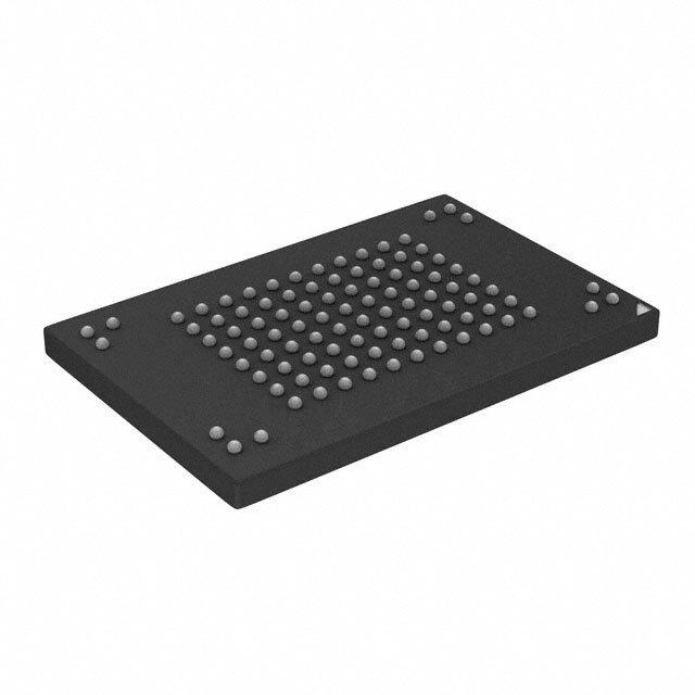
| 供应商器件封装 | 8-SOIC |
| 包装 | 管件 |
| 商标 | Microchip Technology |
| 存储器类型 | FLASH |
| 存储容量 | 4 Mbit |
| 存储类型 | Flash |
| 安装风格 | SMD/SMT |
| 定时类型 | Synchronous |
| 封装 | Tube |
| 封装/外壳 | 8-SOIC(0.154",3.90mm 宽) |
| 封装/箱体 | SOIC-8 |
| 工作温度 | 0 C to + 70 C |
| 工作温度范围 | 0 C to + 70 C |
| 工厂包装数量 | 100 |
| 接口 | SPI 串行 |
| 接口类型 | SPI |
| 数据总线宽度 | 8 bit |
| 最大工作电流 | 10 mA |
| 最大时钟频率 | 50 MHz |
| 标准包装 | 100 |
| 格式-存储器 | 闪存 |
| 电压-电源 | 2.7 V ~ 3.6 V |
| 电源电压-最大 | 3.6 V |
| 电源电压-最小 | 2.7 V |
| 系列 | SST25VF |
| 组织 | 512 k x 8 |
| 结构 | Sector |
| 速度 | 50 MHz |

_renders/IS42S32800D-6BLI.jpg)


- 商务部:美国ITC正式对集成电路等产品启动337调查
- 曝三星4nm工艺存在良率问题 高通将骁龙8 Gen1或转产台积电
- 太阳诱电将投资9.5亿元在常州建新厂生产MLCC 预计2023年完工
- 英特尔发布欧洲新工厂建设计划 深化IDM 2.0 战略
- 台积电先进制程称霸业界 有大客户加持明年业绩稳了
- 达到5530亿美元!SIA预计今年全球半导体销售额将创下新高
- 英特尔拟将自动驾驶子公司Mobileye上市 估值或超500亿美元
- 三星加码芯片和SET,合并消费电子和移动部门,撤换高东真等 CEO
- 三星电子宣布重大人事变动 还合并消费电子和移动部门
- 海关总署:前11个月进口集成电路产品价值2.52万亿元 增长14.8%


PDF Datasheet 数据手册内容提取
SST25VF040B 4 Mbit SPI Serial Flash Features Product Description • Single Voltage Read and Write Operations The 25 series Serial Flash family features a four-wire, - 2.7-3.6V SPI-compatible interface that allows for a low pin-count package which occupies less board space and ulti- • Serial Interface Architecture mately lowers total system costs. The SST25VF040B - SPI Compatible: Mode 0 and Mode 3 devices are enhanced with improved operating fre- • High Speed Clock Frequency quency and even lower power consumption. - Up to 50 MHz SST25VF040B SPI serial flash memories are manu- • Superior Reliability factured with proprietary, high-performance CMOS - Endurance: 100,000 Cycles (typical) SuperFlash technology. The split-gate cell design and thick-oxide tunneling injector attain better reliability and - Greater than 100 years Data Retention manufacturability compared with alternate approaches. • Low Power Consumption: SST25VF040B devices significantly improve perfor- - Active Read Current: 10 mA (typical) mance and reliability, while lowering power consump- - Standby Current: 5 µA (typical) tion. The devices write (Program or Erase) with a single • Flexible Erase Capability power supply of 2.7-3.6V for SST25VF040B. The total - Uniform 4 KByte sectors energy consumed is a function of the applied voltage, - Uniform 32 KByte overlay blocks current, and time of application. Since for any given - Uniform 64 KByte overlay blocks voltage range, the SuperFlash technology uses less • Fast Erase and Byte-Program: current to program and has a shorter erase time, the - Chip-Erase Time: 35 ms (typical) total energy consumed during any Erase or Program - Sector-/Block-Erase Time: 18 ms (typical) operation is less than alternative flash memory technol- - Byte-Program Time: 7 µs (typical) ogies. • Auto Address Increment (AAI) Programming The SST25VF040B device is offered in an 8-lead SOIC - Decrease total chip programming time over (200 mils), 8-lead SOIC (150 mils), and 8-contact Byte-Program operations WSON (6mm x 5mm) packages. See Figure 2-1 for pin assignments. • End-of-Write Detection - Software polling the BUSY bit in Status Register - Busy Status readout on SO pin in AAI Mode • Hold Pin (HOLD#) - Suspends a serial sequence to the memory without deselecting the device • Write Protection (WP#) - Enables/Disables the Lock-Down function of the status register • Software Write Protection - Write protection through Block-Protection bits in status register • Temperature Range - Commercial: 0°C to +70°C - Industrial: -40°C to +85°C • Packages Available - 8-lead SOIC (200 mils) - 8-lead SOIC (150 mils) - 8-contact WSON (6mm x 5mm) • All devices are RoHS compliant 2005-2017 Microchip Technology Inc. DS20005051D-page 1
SST25VF040B TO OUR VALUED CUSTOMERS It is our intention to provide our valued customers with the best documentation possible to ensure successful use of your Microchip products. To this end, we will continue to improve our publications to better suit your needs. Our publications will be refined and enhanced as new volumes and updates are introduced. If you have any questions or comments regarding this publication, please contact the Marketing Communications Department via E- mail at docerrors@microchip.com. We welcome your feedback. Most Current Data Sheet To obtain the most up-to-date version of this data sheet, please register at our Worldwide Web site at: http://www.microchip.com You can determine the version of a data sheet by examining its literature number found on the bottom outside corner of any page. The last character of the literature number is the version number, (e.g., DS30000000A is version A of document DS30000000). Errata An errata sheet, describing minor operational differences from the data sheet and recommended workarounds, may exist for current devices. As device/documentation issues become known to us, we will publish an errata sheet. The errata will specify the revision of silicon and revision of document to which it applies. To determine if an errata sheet exists for a particular device, please check with one of the following: • Microchip’s Worldwide Web site; http://www.microchip.com • Your local Microchip sales office (see last page) When contacting a sales office, please specify which device, revision of silicon and data sheet (include literature number) you are using. Customer Notification System Register on our web site at www.microchip.com to receive the most current information on all of our products. DS20005051D-page 2 2005-2017 Microchip Technology Inc.
SST25VF040B 1.0 BLOCK DIAGRAM FIGURE 1-1: FUNCTIONAL BLOCK DIAGRAM SuperFlash X - Decoder Address Memory Buffers and Latches Y - Decoder I/O Buffers Control Logic and Data Latches Serial Interface CE# SCK SI SO WP# HOLD# 1295 B1.0 2005-2017 Microchip Technology Inc. DS20005051D-page 3
SST25VF040B 2.0 PIN DESCRIPTION FIGURE 2-1: PIN ASSIGNMENTS CE# 1 8 VDD CE# 1 8 VDD SO 2 7 HOLD# SO 2 7 HOLD# Top View Top View WP# 3 6 SCK WP# 3 6 SCK VSS 4 5 SI VSS 4 5 SI 1295 08-soic S2A P1.0 1295 08-wson QA P2.0 8-Lead SOIC 8-Contact WSON TABLE 2-1: PIN DESCRIPTION Symbol Pin Name Functions SCK Serial Clock To provide the timing of the serial interface. Commands, addresses, or input data are latched on the rising edge of the clock input, while output data is shifted out on the falling edge of the clock input. SI Serial Data Input To transfer commands, addresses, or data serially into the device. Inputs are latched on the rising edge of the serial clock. SO Serial Data Output To transfer data serially out of the device. Data is shifted out on the falling edge of the serial clock. Outputs Flash busy status during AAI Programming when reconfigured as RY/BY# pin. See “Hardware End-of-Write Detection” on page11 for details. CE# Chip Enable The device is enabled by a high to low transition on CE#. CE# must remain low for the duration of any command sequence. WP# Write Protect The Write Protect (WP#) pin is used to enable/disable BPL bit in the status register. HOLD# Hold To temporarily stop serial communication with SPI flash memory without resetting the device. V Power Supply To provide power supply voltage: 2.7-3.6V for SST25VF040B DD V Ground SS DS20005051D-page 4 2005-2017 Microchip Technology Inc.
SST25VF040B 3.0 MEMORY ORGANIZATION used to select the device, and data is accessed through the Serial Data Input (SI), Serial Data Output (SO), and The SST25VF040B SuperFlash memory array is orga- Serial Clock (SCK). nized in uniform 4 KByte erasable sectors with 32 The SST25VF040B supports both Mode 0 (0,0) and KByte overlay blocks and 64 KByte overlay erasable Mode 3 (1,1) of SPI bus operations. The difference blocks. between the two modes, as shown in Figure 4-1, is the state of the SCK signal when the bus master is in 4.0 DEVICE OPERATION Stand-by mode and no data is being transferred. The SCK signal is low for Mode 0 and SCK signal is high for The SST25VF040B is accessed through the SPI (Serial Mode 3. For both modes, the Serial Data In (SI) is sam- Peripheral Interface) bus compatible protocol. The SPI pled at the rising edge of the SCK clock signal and the bus consist of four control lines; Chip Enable (CE#) is Serial Data Output (SO) is driven after the falling edge of the SCK clock signal. FIGURE 4-1: SPI PROTOCOL CE# MODE 3 MODE 3 SCK MODE 0 MODE 0 SI Bit 7 Bit 6 Bit 5 Bit 4 Bit 3 Bit 2 Bit 1 Bit 0 DON'T CARE MSB HIGH IMPEDANCE Bit 7 Bit 6 Bit 5 Bit 4 Bit 3 Bit 2 Bit 1 Bit 0 SO MSB 1295 SPIprot.0 4.1 Hold Operation HOLD# signal does not coincide with the SCK active low state, then the device exits in Hold mode when the The HOLD# pin is used to pause a serial sequence SCK next reaches the active low state. See Figure 4-2 underway with the SPI flash memory without resetting for Hold Condition waveform. the clocking sequence. To activate the HOLD# mode, Once the device enters Hold mode, SO will be in high- CE# must be in active low state. The HOLD# mode impedance state while SI and SCK can be V or V begins when the SCK active low state coincides with IL IH. the falling edge of the HOLD# signal. The HOLD mode If CE# is driven active high during a Hold condition, it ends when the HOLD# signal’s rising edge coincides resets the internal logic of the device. As long as with the SCK active low state. HOLD# signal is low, the memory remains in the Hold condition. To resume communication with the device, If the falling edge of the HOLD# signal does not coin- HOLD# must be driven active high, and CE# must be cide with the SCK active low state, then the device driven active low. See Figure 5-3 for Hold timing. enters Hold mode when the SCK next reaches the active low state. Similarly, if the rising edge of the FIGURE 4-2: HOLD CONDITION WAVEFORM SCK HOLD# Active Hold Active Hold Active 1295 HoldCond.0 2005-2017 Microchip Technology Inc. DS20005051D-page 5
SST25VF040B 4.2 Write Protection 4.2.1 WRITE PROTECT PIN (WP#) SST25VF040B provides software Write protection. The The Write Protect (WP#) pin enables the lock-down Write Protect pin (WP#) enables or disables the lock- function of the BPL bit (bit 7) in the status register. down function of the status register. The Block-Protec- When WP# is driven low, the execution of the Write- tion bits (BP3, BP2, BP1, BP0, and BPL) in the status Status-Register (WRSR) instruction is determined by register provide Write protection to the memory array the value of the BPL bit (see Table 4-1). When WP# is and the status register. See Table 4-3 for the Block-Pro- high, the lock-down function of the BPL bit is disabled. tection description. TABLE 4-1: CONDITIONS TO EXECUTE WRITE-STATUS-REGISTER (WRSR) INSTRUCTION WP# BPL Execute WRSR Instruction L 1 Not Allowed L 0 Allowed H X Allowed 4.3 Status Register During an internal Erase or Program operation, the sta- tus register may be read only to determine the comple- The software status register provides status on tion of an operation in progress. Table 4-2 describes whether the flash memory array is available for any the function of each bit in the software status register. Read or Write operation, whether the device is Write enabled, and the state of the Memory Write protection. TABLE 4-2: SOFTWARE STATUS REGISTER Default at Bit Name Function Power-up Read/Write 0 BUSY 1 = Internal Write operation is in progress 0 R 0 = No internal Write operation is in progress 1 WEL 1 = Device is memory Write enabled 0 R 0 = Device is not memory Write enabled 2 BP0 Indicate current level of block write protection (See Table 4-3) 1 R/W 3 BP1 Indicate current level of block write protection (See Table 4-3) 1 R/W 4 BP2 Indicate current level of block write protection (See Table 4-3) 1 R/W 5 BP3 Indicate current level of block write protection (See Table 4-3) 0 R/W 6 AAI Auto Address Increment Programming status 0 R 1 = AAI programming mode 0 = Byte-Program mode 7 BPL 1 = BP3, BP2, BP1, BP0 are read-only bits 0 R/W 0 = BP3, BP2, BP1, BP0 are read/writable 4.3.1 BUSY any memory Write (Program/Erase) commands. The Write-Enable-Latch bit is automatically reset under the The Busy bit determines whether there is an internal following conditions: Erase or Program operation in progress. A “1” for the Busy bit indicates the device is busy with an operation • Power-up in progress. A “0” indicates the device is ready for the • Write-Disable (WRDI) instruction completion next valid operation. • Byte-Program instruction completion • Auto Address Increment (AAI) programming is 4.3.2 WRITE ENABLE LATCH (WEL) completed or reached its highest unprotected The Write-Enable-Latch bit indicates the status of the memory address internal memory Write Enable Latch. If the Write- • Sector-Erase instruction completion Enable-Latch bit is set to “1”, it indicates the device is • Block-Erase instruction completion Write enabled. If the bit is set to “0” (reset), it indicates the device is not Write enabled and does not accept • Chip-Erase instruction completion • Write-Status-Register instructions DS20005051D-page 6 2005-2017 Microchip Technology Inc.
SST25VF040B 4.3.3 AUTO ADDRESS INCREMENT (AAI) BP1 and BP0 bits as long as WP# is high or the Block- Protect-Lock (BPL) bit is 0. Chip-Erase can only be The Auto Address Increment Programming-Status bit executed if Block-Protection bits are all 0. After power- provides status on whether the device is in AAI pro- up, BP3, BP2, BP1 and BP0 are set to 1. gramming mode or Byte-Program mode. The default at power up is Byte-Program mode. 4.3.5 BLOCK PROTECTION LOCK-DOWN (BPL) 4.3.4 BLOCK PROTECTION (BP3,BP2, BP1, BP0) WP# pin driven low (V ), enables the Block-Protection- IL Lock-Down (BPL) bit. When BPL is set to 1, it prevents The Block-Protection (BP3, BP2, BP1, BP0) bits define any further alteration of the BPL, BP3, BP2, BP1, and the size of the memory area, as defined in Table 4-3, to BP0 bits. When the WP# pin is driven high (V ), the be software protected against any memory Write (Pro- IH BPL bit has no effect and its value is “Don’t Care”. After gram or Erase) operation. The Write-Status-Register power-up, the BPL bit is reset to 0. (WRSR) instruction is used to program the BP3, BP2, TABLE 4-3: SOFTWARE STATUS REGISTER BLOCK PROTECTION FOR SST25VF040B1 Status Register Bit2 Protected Memory Address Protection Level BP3 BP2 BP1 BP0 4 Mbit None X 0 0 0 None Upper 1/8 X 0 0 1 70000H-7FFFFH Upper 1/4 X 0 1 0 60000H-7FFFFH Upper 1/2 X 0 1 1 40000H-7FFFFH All Blocks X 1 0 0 00000H-7FFFFH All Blocks X 1 0 1 00000H-7FFFFH All Blocks X 1 1 0 00000H-7FFFFH All Blocks X 1 1 1 00000H-7FFFFH 1. X = Don’t Care (RESERVED) default is “0 2. Default at power-up for BP2, BP1, and BP0 is ‘111’. (All Blocks Protected) 2005-2017 Microchip Technology Inc. DS20005051D-page 7
SST25VF040B 4.4 Instructions of CE#. Inputs will be accepted on the rising edge of SCK starting with the most significant bit. CE# must be Instructions are used to read, write (Erase and Pro- driven low before an instruction is entered and must be gram), and configure the SST25VF040B. The instruc- driven high after the last bit of the instruction has been tion bus cycles are 8 bits each for commands (Op shifted in (except for Read, Read-ID, and Read-Status- Code), data, and addresses. Prior to executing any Register instructions). Any low to high transition on Byte-Program, Auto Address Increment (AAI) program- CE#, before receiving the last bit of an instruction bus ming, Sector-Erase, Block-Erase, Write-Status-Regis- cycle, will terminate the instruction in progress and ter, or Chip-Erase instructions, the Write-Enable return the device to standby mode. Instruction com- (WREN) instruction must be executed first. The com- mands (Op Code), addresses, and data are all input plete list of instructions is provided in Table 4-4. All from the most significant bit (MSB) first. instructions are synchronized off a high to low transition TABLE 4-4: DEVICE OPERATION INSTRUCTIONS Address Dummy Data Instruction Description Op Code Cycle1 Cycle(s)2 Cycle(s) Cycle(s) Read Read Memory 0000 0011b (03H) 3 0 1 to High-Speed Read Read Memory at higher speed 0000 1011b (0BH) 3 1 1 to 4 KByte Sector- Erase 4 KByte of memory array 0010 0000b (20H) 3 0 0 Erase3 32 KByte Block- Erase 32 KByte block of memory 0101 0010b (52H) 3 0 0 Erase4 array 64 KByte Block- Erase 64 KByte block of memory 1101 1000b (D8H) 3 0 0 Erase5 array Chip-Erase Erase Full Memory Array 0110 0000b (60H) 0 0 0 or 1100 0111b (C7H) Byte-Program To Program One Data Byte 0000 0010b (02H) 3 0 1 AAI-Word-Program6 Auto Address Increment Program- 1010 1101b (ADH) 3 0 2 to ming RDSR7 Read-Status-Register 0000 0101b (05H) 0 0 1 to EWSR Enable-Write-Status-Register 0101b 0000b (50H) 0 0 0 WRSR Write-Status-Register 0000 0001b (01H) 0 0 1 WREN Write-Enable 0000 0110b (06H) 0 0 0 WRDI Write-Disable 0000 0100b (04H) 0 0 0 RDID8 Read-ID 1001 0000b (90H) 3 0 1 to or 1010 1011b (ABH) JEDEC-ID JEDEC ID read 1001 1111b (9FH) 0 0 3 to EBSY Enable SO to output RY/BY# status 0111 0000b (70H) 0 0 0 during AAI programming DBSY Disable SO as RY/BY# 1000 0000b (80H) 0 0 0 status during AAI programming 1. One bus cycle is eight clock periods. 2. Address bits above the most significant bit of each density can be V or V . IL IH 3. 4KByte Sector Erase addresses: use A -A remaining addresses are don’t care but must be set either at V or V MS 12, IL IH. 4. 32KByte Block Erase addresses: use A -A remaining addresses are don’t care but must be set either at V or V MS 15, IL IH. 5. 64KByte Block Erase addresses: use A -A remaining addresses are don’t care but must be set either at V or V MS 16, IL IH. 6. To continue programming to the next sequential address location, enter the 8-bit command, ADH, followed by 2 bytes of data to be programmed. Data Byte 0 will be programmed into the initial address [A -A ] with A =0, Data Byte 1 will be pro- 23 1 0 grammed into the initial address [A -A ] with A =1. 23 1 0 7. The Read-Status-Register is continuous with ongoing clock cycles until terminated by a low to high transition on CE#. 8. Manufacturer’s ID is read with A =0, and Device ID is read with A =1. All other address bits are 00H. The Manufacturer’s ID 0 0 and device ID output stream is continuous until terminated by a low-to-high transition on CE#. DS20005051D-page 8 2005-2017 Microchip Technology Inc.
SST25VF040B 4.4.1 READ (25 MHZ) cally increment to the beginning (wrap-around) of the address space. Once the data from address location The Read instruction, 03H, supports up to 25 MHz 1FFFFFH has been read, the next output will be from Read. The device outputs the data starting from the address location 000000H. specified address location. The data output stream is continuous through all addresses until terminated by a The Read instruction is initiated by executing an 8-bit low to high transition on CE#. The internal address command, 03H, followed by address bits [A23-A0]. CE# pointer will automatically increment until the highest must remain active low for the duration of the Read memory address is reached. Once the highest memory cycle. See Figure 4-3 for the Read sequence. address is reached, the address pointer will automati- FIGURE 4-3: READ SEQUENCE CE# MODE 3 0 1 2 3 4 5 6 7 8 1516 2324 3132 3940 47 48 5556 6364 70 SCK MODE 0 03 ADD. ADD. ADD. SI MSB MSB N N+1 N+2 N+3 N+4 HIGH IMPEDANCE SO DOUT DOUT DOUT DOUT DOUT MSB 1295 ReadSeq.0 4.4.2 HIGH-SPEED-READ (50 MHZ) through all addresses until terminated by a low to high transition on CE#. The internal address pointer will The High-Speed-Read instruction supporting up to 50 automatically increment until the highest memory MHz Read is initiated by executing an 8-bit command, address is reached. Once the highest memory address 0BH, followed by address bits [A -A ] and a dummy 23 0 is reached, the address pointer will automatically incre- byte. CE# must remain active low for the duration of the ment to the beginning (wrap-around) of the address High-Speed-Read cycle. See Figure 4-4 for the High- space. Once the data from address location 7FFFFH Speed-Read sequence. has been read, the next output will be from address Following a dummy cycle, the High-Speed-Read location 00000H. instruction outputs the data starting from the specified address location. The data output stream is continuous FIGURE 4-4: HIGH-SPEED-READ SEQUENCE CE# MODE 3 0 1 2 3 4 5 6 7 8 1516 23 24 3132 3940 4748 55 56 6364 7172 80 SCK MODE 0 SI 0B ADD. ADD. ADD. X MSB MSB N N+1 N+2 N+3 N+4 SO HIGH IMPEDANCE DOUT DOUT DOUT DOUT DOUT MSB Note: X = Dummy Byte: 8 Clocks Input Dummy Cycle (VIL or VIH) 1295 HSRdSeq.0 2005-2017 Microchip Technology Inc. DS20005051D-page 9
SST25VF040B 4.4.3 BYTE-PROGRAM The Byte-Program instruction is initiated by executing an 8-bit command, 02H, followed by address bits [A - The Byte-Program instruction programs the bits in the 23 A ]. Following the address, the data is input in order selected byte to the desired data. The selected byte 0 from MSB (bit 7) to LSB (bit 0). CE# must be driven must be in the erased state (FFH) when initiating a Pro- high before the instruction is executed. The user may gram operation. A Byte-Program instruction applied to a poll the Busy bit in the software status register or wait protected memory area will be ignored. T for the completion of the internal self-timed Byte- BP Prior to any Write operation, the Write-Enable (WREN) Program operation. See Figure 4-5 for the Byte-Pro- instruction must be executed. CE# must remain active gram sequence. low for the duration of the Byte-Program instruction. FIGURE 4-5: BYTE-PROGRAM SEQUENCE CE# MODE 3 0 1 2 3 4 5 6 7 8 1516 2324 3132 39 SCK MODE 0 SI 02 ADD. ADD. ADD. DIN MSB MSB MSB LSB SO HIGH IMPEDANCE 1295 ByteProg.0 4.4.4 AUTO ADDRESS INCREMENT (AAI) device indicates it is no longer busy, data for the next WORD-PROGRAM two sequential addresses may be programmed, fol- lowed by the next two, and so on. The AAI program instruction allows multiple bytes of data to be programmed without re-issuing the next When programming the last desired word, or the high- sequential address location. This feature decreases est unprotected memory address, check the busy sta- total programming time when multiple bytes or entire tus using either the hardware or software (RDSR memory array is to be programmed. An AAI Word pro- instruction) method to check for program completion. gram instruction pointing to a protected memory area Once programming is complete, use the applicable will be ignored. The selected address range must be in method to terminate AAI. If the device is in Software the erased state (FFH) when initiating an AAI Word End-of-Write Detection mode, execute the Write-Dis- Program operation. While within AAI Word Program- able (WRDI) instruction, 04H. If the device is in AAI ming sequence, only the following instructions are Hardware End-of-Write Detection mode, execute the valid: for software end-of-write detection—AAI Word Write-Disable (WRDI) instruction, 04H, followed by the (ADH), WRDI (04H), and RDSR (05H); for hardware 8-bit DBSY command, 80H. There is no wrap mode end-of-write detection—AAI Word (ADH) and WRDI during AAI programming once the highest unprotected (04H). There are three options to determine the com- memory address is reached. See Figures 4-8 and 4-9 pletion of each AAI Word program cycle: hardware for the AAI Word programming sequence. detection by reading the Serial Output, software detec- 4.4.5 END-OF-WRITE DETECTION tion by polling the BUSY bit in the software status reg- ister, or wait TBP. Refer to“End-of-Write Detection” for There are three methods to determine completion of a details. program cycle during AAI Word programming: hard- Prior to any write operation, the Write-Enable (WREN) ware detection by reading the Serial Output, software instruction must be executed. Initiate the AAI Word detection by polling the BUSY bit in the Software Status Program instruction by executing an 8-bit command, Register, or wait TBP. The Hardware End-of-Write detection method is described in the section below. ADH, followed by address bits [A -A ]. Following the 23 0 addresses, two bytes of data are input sequentially, each one from MSB (Bit 7) to LSB (Bit 0). The first byte of data (D0) is programmed into the initial address [A - 23 A ] with A =0, the second byte of Data (D1) is pro- 1 0 grammed into the initial address [A -A ] with A =1. 23 1 0 CE# must be driven high before executing the AAI Word Program instruction. Check the BUSY status before entering the next valid command. Once the DS20005051D-page 10 2005-2017 Microchip Technology Inc.
SST25VF040B 4.4.6 HARDWARE END-OF-WRITE on the SO pin. A ‘0’ indicates the device is busy and a DETECTION ‘1’ indicates the device is ready for the next instruction. De-asserting CE# will return the SO pin to tri-state. The Hardware End-of-Write detection method elimi- While in AAI and Hardware End-of-Write detection nates the overhead of polling the Busy bit in the Soft- mode, the only valid instructions are AAI Word (ADH) ware Status Register during an AAI Word program and WRDI (04H). operation. The 8-bit command, 70H, configures the Serial Output (SO) pin to indicate Flash Busy status To exit AAI Hardware End-of-Write detection, first exe- during AAI Word programming. (see Figure 4-6) The 8- cute WRDI instruction, 04H, to reset the Write-Enable- bit command, 70H, must be executed prior to initiating Latch bit (WEL=0) and AAI bit. Then execute the 8-bit an AAI Word-Program instruction. Once an internal DBSY command, 80H, to disable RY/BY# status during programming operation begins, asserting CE# will the AAI command. See Figures 4-7 and 4-8. immediately drive the status of the internal flash status FIGURE 4-6: ENABLE SO AS HARDWARE RY/BY# DURING AAI PROGRAMMING CE# MODE 3 0 1 2 3 4 5 6 7 SCK MODE 0 70 SI MSB SO HIGH IMPEDANCE 1295 EnableSO.0 FIGURE 4-7: DISABLE SO AS HARDWARE RY/BY# DURING AAI PROGRAMMING CE# MODE 3 0 1 2 3 4 5 6 7 SCK MODE 0 80 SI MSB SO HIGH IMPEDANCE 1295 DisableSO.0 2005-2017 Microchip Technology Inc. DS20005051D-page 11
SST25VF040B FIGURE 4-8: AUTO ADDRESS INCREMENT (AAI) WORD-PROGRAM SEQUENCE WITH HARDWARE END-OF-WRITE DETECTION CE# MODE 3 0 7 0 7 0 7 8 1516 2324 3132 3940 47 0 7 8 1516 23 SCKMODE 0 SI EBSY WREN AD A A A D0 D1 AD D2 D3 Load AAI command, Address, 2 bytes data SO Check for Flash Busy Status to load next valid1 command CE# cont. 0 7 8 1516 23 0 7 0 7 0 7 8 15 SCK cont. SI cont. AD Dn-1 Dn WRDI DBSY RDSR Last 2 WRDI followed by DBSY Data Bytes to exit AAI Mode SO cont. DOUT Check for Flash Busy Status to load next valid1 command 1295 AAI.HW.3 Note: 1. Valid commands during AAI programming: AAI command or WRDI command 2. User must configure the SO pin to output Flash Busy status during AAI programming FIGURE 4-9: AUTO ADDRESS INCREMENT (AAI) WORD-PROGRAM SEQUENCE WITH SOFTWARE END-OF-WRITE DETECTION Wait TBP or poll Software Status register to load next valid1 command CE# MODE 3 0 7 8 1516 2324 3132 3940 47 0 7 8 1516 23 0 7 8 1516 23 0 7 0 7 8 15 SCK MODE 0 SI AD A A A D0 D1 AD D2 D3 AD Dn-1 Dn WRDI RDSR Load AAI command, Address, 2 bytes data Last 2 WRDI to exit Data Bytes AAI Mode SO DOUT 1295 AAI.SW.1 Note: 1. Valid commands during AAI programming: AAI command or WRDI command DS20005051D-page 12 2005-2017 Microchip Technology Inc.
SST25VF040B 4.4.7 4-KBYTE SECTOR-ERASE bits [A -A ]. Address bits [A -A ] (A =Most Sig- 23 0 MS 12 MS nificant address) are used to determine the sector The Sector-Erase instruction clears all bits in the address (SA ), remaining address bits can be V or V selected 4 KByte sector to FFH. A Sector-Erase X IL IH. CE# must be driven high before the instruction is exe- instruction applied to a protected memory area will be cuted. The user may poll the Busy bit in the software ignored. Prior to any Write operation, the Write-Enable status register or wait T for the completion of the (WREN) instruction must be executed. CE# must SE internal self-timed Sector-Erase cycle. See Figure 4-10 remain active low for the duration of any command for the Sector-Erase sequence. sequence. The Sector-Erase instruction is initiated by executing an 8-bit command, 20H, followed by address FIGURE 4-10: SECTOR-ERASE SEQUENCE CE# MODE 3 0 1 2 3 4 5 6 7 8 1516 2324 31 SCK MODE 0 20 ADD. ADD. ADD. SI MSB MSB SO HIGH IMPEDANCE 1295 SecErase.0 4.4.8 32-KBYTE AND 64-KBYTE BLOCK- nificant Address) are used to determine block address ERASE (BAX), remaining address bits can be VIL or VIH. CE# must be driven high before the instruction is executed. The The 32-KByte Block-Erase instruction clears all bits in 64-KByte Block-Erase instruction is initiated by executing an the selected 32 KByte block to FFH. A Block-Erase 8-bit command D8H, followed by address bits [A -A ]. instruction applied to a protected memory area will be 23 0 Address bits [A -A ] are used to determine block address ignored. The 64-KByte Block-Erase instruction clears all bits MS 16 (BA ), remaining address bits can be V or V CE# must in the selected 64 KByte block to FFH. A Block-Erase X IL IH. be driven high before the instruction is executed. The user instruction applied to a protected memory area will be may poll the Busy bit in the software status register or wait ignored. Prior to any Write operation, the Write-Enable T for the completion of the internal self-timed 32- (WREN) instruction must be executed. CE# must remain BE KByte Block-Erase or 64-KByte Block-Erase cycles. active low for the duration of any command sequence. See Figures 4-11 and 4-12 for the 32-KByte Block- The 32-KByte Block-Erase instruction is initiated by Erase and 64-KByte Block-Erase sequences. executing an 8-bit command, 52H, followed by address bits [A -A ]. Address bits [A -A ] (A =Most Sig- 23 0 MS 15 MS FIGURE 4-11: 32-KBYTE BLOCK-ERASE SEQUENCE CE# MODE 3 0 1 2 3 4 5 6 7 8 1516 2324 31 SCK MODE 0 52 ADDR ADDR ADDR SI MSB MSB SO HIGH IMPEDANCE 1295 32KBklEr.0 2005-2017 Microchip Technology Inc. DS20005051D-page 13
SST25VF040B FIGURE 4-12: 64-KBYTE BLOCK-ERASE SEQUENCE CE# MODE 3 0 1 2 3 4 5 6 7 8 1516 2324 31 SCK MODE 0 D8 ADDR ADDR ADDR SI MSB MSB SO HIGH IMPEDANCE 1295 63KBlkEr.0 4.4.9 CHIP-ERASE instruction is initiated by executing an 8-bit command, 60H or C7H. CE# must be driven high before the instruction The Chip-Erase instruction clears all bits in the device is executed. The user may poll the Busy bit in the software to FFH. A Chip-Erase instruction will be ignored if any status register or wait T for the completion of the of the memory area is protected. Prior to any Write oper- CE internal self-timed Chip-Erase cycle. See Figure 4-13 ation, the Write-Enable (WREN) instruction must be exe- for the Chip-Erase sequence. cuted. CE# must remain active low for the duration of the Chip-Erase instruction sequence. The Chip-Erase FIGURE 4-13: CHIP-ERASE SEQUENCE CE# MODE 3 0 1 2 3 4 5 6 7 SCK MODE 0 60 or C7 SI MSB SO HIGH IMPEDANCE 1295 ChEr.0 DS20005051D-page 14 2005-2017 Microchip Technology Inc.
SST25VF040B 4.4.10 READ-STATUS-REGISTER (RDSR) properly received by the device. CE# must be driven low before the RDSR instruction is entered and remain The Read-Status-Register (RDSR) instruction allows low until the status data is read. Read-Status-Register reading of the status register. The status register may is continuous with ongoing clock cycles until it is termi- be read at any time even during a Write (Program/ nated by a low to high transition of the CE#. See Figure Erase) operation. When a Write operation is in prog- 4-14 for the RDSR instruction sequence. ress, the Busy bit may be checked before sending any new commands to assure that the new commands are FIGURE 4-14: READ-STATUS-REGISTER (RDSR) SEQUENCE CE# MODE 3 0 1 2 3 4 5 6 7 8 9 10 11 12 13 14 SCK MODE 0 05 SI MSB HIGH IMPEDANCE Bit 7 Bit 6 Bit 5 Bit 4 Bit 3 Bit 2 Bit 1 Bit 0 SO MSB Status 1295 RDSRseq.0 Register Out 4.4.11 WRITE-ENABLE (WREN) execution of the Write-Status-Register (WRSR) instruc- tion; however, the Write-Enable-Latch bit in the Status The Write-Enable (WREN) instruction sets the Write- Register will be cleared upon the rising edge CE# of the Enable-Latch bit in the Status Register to 1 allowing WRSR instruction. CE# must be driven high before the Write operations to occur. The WREN instruction must WREN instruction is executed. be executed prior to any Write (Program/Erase) opera- tion. The WREN instruction may also be used to allow FIGURE 4-15: WRITE ENABLE (WREN) SEQUENCE CE# MODE 3 0 1 2 3 4 5 6 7 SCK MODE 0 06 SI MSB SO HIGH IMPEDANCE 1295 WREN.0 2005-2017 Microchip Technology Inc. DS20005051D-page 15
SST25VF040B 4.4.12 WRITE-DISABLE (WRDI) ress. Any program operation in progress may continue up to T after executing the WRDI instruction. CE# The Write-Disable (WRDI) instruction resets the Write- BP must be driven high before the WRDI instruction is exe- Enable-Latch bit and AAI bit to 0 disabling any new cuted. Write operations from occurring. The WRDI instruction will not terminate any programming operation in prog- CE# MODE 3 0 1 2 3 4 5 6 7 SCK MODE 0 04 SI MSB SO HIGH IMPEDANCE 1295 WRDI.0 FIGURE 4-16: WRITE DISABLE (WRDI) SEQUENCE 4.4.13 ENABLE-WRITE-STATUS- command sequence of the WRSR instruction is REGISTER (EWSR) entered and driven high before the WRSR instruction is executed. See Figure 4-17 for EWSR or WREN and The Enable-Write-Status-Register (EWSR) instruction WRSR instruction sequences. arms the Write-Status-Register (WRSR) instruction and opens the status register for alteration. The Write- Executing the Write-Status-Register instruction will be Status-Register instruction must be executed immedi- ignored when WP# is low and BPL bit is set to “1”. ately after the execution of the Enable-Write-Status- When the WP# is low, the BPL bit can only be set from Register instruction. This two-step instruction “0” to “1” to lock-down the status register, but cannot be sequence of the EWSR instruction followed by the reset from “1” to “0”. When WP# is high, the lock-down WRSR instruction works like SDP (software data pro- function of the BPL bit is disabled and the BPL, BP0, tection) command structure which prevents any acci- and BP1 and BP2 bits in the status register can all be dental alteration of the status register values. CE# must changed. As long as BPL bit is set to 0 or WP# pin is be driven low before the EWSR instruction is entered driven high (VIH) prior to the low-to-high transition of the and must be driven high before the EWSR instruction CE# pin at the end of the WRSR instruction, the bits in is executed. the status register can all be altered by the WRSR instruction. In this case, a single WRSR instruction can 4.4.14 WRITE-STATUS-REGISTER (WRSR) set the BPL bit to “1” to lock down the status register as well as altering the BP0, BP1, and BP2 bits at the same The Write-Status-Register instruction writes new val- time. See Table 4-1 for a summary description of WP# ues to the BP3, BP2, BP1, BP0, and BPL bits of the sta- and BPL functions. tus register. CE# must be driven low before the FIGURE 4-17: ENABLE-WRITE-STATUS-REGISTER (EWSR) OR WRITE-ENABLE (WREN) AND WRITE-STATUS-REGISTER (WRSR) SEQUENCE CE# MODE 3 0 1 2 3 4 5 6 7 MODE 3 0 1 2 3 4 5 6 7 8 9 101112131415 SCK MODE 0 MODE 0 STATUS REGISTER IN 50 or 06 01 7 6 5 4 3 2 1 0 SI MSB MSB MSB HIGH IMPEDANCE SO 1295 EWSR.0 DS20005051D-page 16 2005-2017 Microchip Technology Inc.
SST25VF040B 4.4.15 JEDEC READ-ID out on the SO pin. Byte 1, BFH, identifies the manufac- turer as Microchip. Byte 2, 25H, identifies the memory The JEDEC Read-ID instruction identifies the device as type as SPI Serial Flash. Byte 3, 8DH, identifies the SST25VF040B and the manufacturer as Microchip. device as SST25VF040B. The instruction sequence is The device information can be read from executing the shown in Figure 4-18. The JEDEC Read ID instruction 8-bit command, 9FH. Following the JEDEC Read-ID is terminated by a low to high transition on CE# at any instruction, the 8-bit manufacturer’s ID, BFH, is output time during data output. from the device. After that, a 16-bit device ID is shifted FIGURE 4-18: JEDEC READ-ID SEQUENCE CE# MODE 3 0 1 2 3 4 5 6 7 8 9 10111213141516171819202122232425262728293031323334 SCK MODE 0 SI 9F HIGH IMPEDANCE BF 25 8D SO MSB MSB 1295 JEDECID.1 TABLE 4-5: JEDEC READ-ID DATA Manufacturer’s ID Device ID Memory Type Memory Capacity Byte1 Byte 2 Byte 3 BFH 25H 8DH 2005-2017 Microchip Technology Inc. DS20005051D-page 17
SST25VF040B 4.4.16 READ-ID (RDID) Read-ID instruction, the manufacturer’s ID is located in address 00000H and the device ID is located in The Read-ID instruction (RDID) identifies the devices address 00001H. Once the device is in Read-ID mode, as SST25VF040B and manufacturer as Microchip. This the manufacturer’s and device ID output data toggles command is backward compatible to all SST25xFxxxA between address 00000H and 00001H until terminated devices and should be used as default device identifi- by a low to high transition on CE#. cation when multiple versions of SPI Serial Flash devices are used in a design. The device information Refer to Tables 4-5 and 4-6 for device identification can be read from executing an 8-bit command, 90H or data. ABH, followed by address bits [A -A ]. Following the 23 0 FIGURE 4-19: READ-ID SEQUENCE CE# MODE 3 0 1 2 3 4 5 6 7 8 1516 2324 3132 3940 4748 5556 63 SCK MODE 0 90 or AB 00 00 ADD1 SI MSB MSB HIGH HIGH IMPEDANCE IMPEDANCE SO BF Device ID BF Device ID MSB Note: The manufacturer's and device ID output stream is continuous until terminated by a low to high transition on CE#. Device ID = 8DH for SST25VF040B 1. 00H will output the manfacturer's ID first and 01H will output device ID first before toggling between the two. 1295 RdID.0 TABLE 4-6: PRODUCT IDENTIFICATION Address Data Manufacturer’s ID 00000H BFH Device ID SST25VF040B 00001H 8DH DS20005051D-page 18 2005-2017 Microchip Technology Inc.
SST25VF040B 5.0 ELECTRICAL SPECIFICATIONS Absolute Maximum Stress Ratings (Applie3d conditions greater than those listed under “Absolute Max- imum Stress Ratings” may cause permanent damage to the device. This is a stress rating only and func- tional operation of the device at these conditions or conditions greater than those defined in the operational sections of this data sheet is not implied. Exposure to absolute maximum stress rating conditions may affect device reliability.) Temperature Under Bias . . . . . . . . . . . . . . . . . . . . . . . . . . . . . . . . . . . . . . . . . . . . . . . . . -55°C to +125°C Storage Temperature . . . . . . . . . . . . . . . . . . . . . . . . . . . . . . . . . . . . . . . . . . . . . . . . . . . . -65°C to +150°C D. C. Voltage on Any Pin to Ground Potential . . . . . . . . . . . . . . . . . . . . . . . . . . . . . . . .-0.5V to V +0.5V DD Transient Voltage (<20 ns) on Any Pin to Ground Potential. . . . . . . . . . . . . . . . . . . . . .-2.0V to V +2.0V DD Package Power Dissipation Capability (T = 25°C). . . . . . . . . . . . . . . . . . . . . . . . . . . . . . . . . . . . . . 1.0W A Surface Mount Solder Reflow Temperature. . . . . . . . . . . . . . . . . . . . . . . . . . . . . . . 260°C for 10 seconds Output Short Circuit Current1. . . . . . . . . . . . . . . . . . . . . . . . . . . . . . . . . . . . . . . . . . . . . . . . . . . . . . 50 mA 1. Output shorted for no more than one second. No more than one output shorted at a time. TABLE 5-1: OPERATING RANGE TABLE 5-2: AC CONDITIONS OF TEST1 Range Ambient Temp V Input Rise/Fall Time Output Load DD Commercial 0°C to +70°C 2.7-3.6V 5ns C = 30 pF L Industrial -40°C to +85°C 2.7-3.6V 1. See Figures 5-5 and 5-6 TABLE 5-3: DC OPERATING CHARACTERISTICS Limits Symbol Parameter Min Max Units Test Conditions I Read Current 10 mA CE#=0.1 V /0.9 V @25 MHz, SO=open DDR DD DD I Read Current 15 mA CE#=0.1 V /0.9 V @50 MHz, SO=open DDR2 DD DD I Program and Erase Current 30 mA CE#=V DDW DD I Standby Current 20 µA CE#=V , V =V or V SB DD IN DD SS I Input Leakage Current 1 µA V =GND to V , V =V Max LI IN DD DD DD I Output Leakage Current 1 µA V =GND to V , V =V Max LO OUT DD DD DD V Input Low Voltage 0.8 V V =V Min IL DD DD V Input High Voltage 0.7 V V V =V Max IH DD DD DD V Output Low Voltage 0.2 V I =100 µA, V =V Min OL OL DD DD V Output Low Voltage 0.4 V I =1.6 mA, V =V Min OL2 OL DD DD V Output High Voltage V -0.2 V I =-100 µA, V =V Min OH DD OH DD DD TABLE 5-4: CAPACITANCE (T = 25°C, F=1 MHz, OTHER PINS OPEN) A Parameter Description Test Condition Maximum C 1 Output Pin Capacitance V = 0V 12 pF OUT OUT C 1 Input Capacitance V = 0V 6 pF IN IN 1. This parameter is measured only for initial qualification and after a design or process change that could affect this parameter. 2005-2017 Microchip Technology Inc. DS20005051D-page 19
SST25VF040B TABLE 5-5: RELIABILITY CHARACTERISTICS Symbol Parameter Minimum Specification Units Test Method N 1 Endurance 10,000 Cycles JEDEC Standard A117 END T 1 Data Retention 100 Years JEDEC Standard A103 DR I 1 Latch Up 100 + I mA JEDEC Standard 78 LTH DD 1. This parameter is measured only for initial qualification and after a design or process change that could affect this parameter. TABLE 5-6: AC OPERATING CHARACTERISTICS 25 MHz 50 MHz Symbol Parameter Min Max Min Max Units F 1 Serial Clock Frequency 25 50 MHz CLK T Serial Clock High Time 18 9 ns SCKH T Serial Clock Low Time 18 9 ns SCKL T 2 Serial Clock Rise Time (Slew Rate) 0.1 0.1 V/ns SCKR T Serial Clock Fall Time (Slew Rate) 0.1 0.1 V/ns SCKF T 3 CE# Active Setup Time 10 5 ns CES T 3 CE# Active Hold Time 10 5 ns CEH T 3 CE# Not Active Setup Time 10 5 ns CHS T 3 CE# Not Active Hold Time 10 5 ns CHH T CE# High Time 100 50 ns CPH T CE# High to High-Z Output 15 8 ns CHZ T SCK Low to Low-Z Output 0 0 ns CLZ T Data In Setup Time 5 2 ns DS T Data In Hold Time 5 5 ns DH T HOLD# Low Setup Time 10 5 ns HLS T HOLD# High Setup Time 10 5 ns HHS T HOLD# Low Hold Time 10 5 ns HLH T HOLD# High Hold Time 10 5 ns HHH T HOLD# Low to High-Z Output 20 8 ns HZ T HOLD# High to Low-Z Output 15 8 ns LZ T Output Hold from SCK Change 0 0 ns OH T Output Valid from SCK 15 8 ns V T Sector-Erase 25 25 ms SE T Block-Erase 25 25 ms BE T Chip-Erase 50 50 ms SCE T Byte-Program 10 10 µs BP 1. Maximum clock frequency for Read Instruction, 03H, is 25 MHz 2. Maximum Rise and Fall time may be limited by T and T requirements SCKH SCKL 3. Relative to SCK. DS20005051D-page 20 2005-2017 Microchip Technology Inc.
SST25VF040B FIGURE 5-1: SERIAL INPUT TIMING DIAGRAM TCPH CE# TCHH TCES TSCKF TCEH TCHS SCK TDS TDH TSCKR MSB LSB SI SO HIGH-Z HIGH-Z 1295 SerIn.0 FIGURE 5-2: SERIAL OUTPUT TIMING DIAGRAM CE# TSCKH TSCKL SCK TOH TCLZ TCHZ SO MSB LSB TV SI 1295 SerOut.0 FIGURE 5-3: HOLD TIMING DIAGRAM CE# THHH THLS THHS SCK THLH THZ TLZ SO SI HOLD# 1295 Hold.0 2005-2017 Microchip Technology Inc. DS20005051D-page 21
SST25VF040B 5.1 Power-Up Specifications All functionalities and DC specifications are specified for a V ramp rate of greater than 1V per 100 ms (0v DD - 3.0V in less than 300 ms). See Table 5-7 and Figure 5-4 for more information. TABLE 5-7: RECOMMENDED SYSTEM POWER-UP TIMINGS Symbol Parameter Minimum Units T 1 V Min to Read Operation 100 µs PU-READ DD T 1 V Min to Write Operation 100 µs PU-WRITE DD 1. This parameter is measured only for initial qualification and after a design or process change that could affect this parame- ter. FIGURE 5-4: POWER-UP TIMING DIAGRAM VDD VDD Max Chip selection is not allowed. Commands may not be accepted or properly interpreted by the device. VDD Min TPU-READ Device fully accessible TPU-WRITE Time 1295 PwrUp.0 FIGURE 5-5: AC INPUT/OUTPUT REFERENCE WAVEFORMS VIHT VHT VHT INPUT? REFERENCE POINTS OUTPUT VLT VLT VILT 1295 IORef.0 AC test inputs are driven at V (0.9V ) for a logic “1” and V (0.1V ) for a logic “0”. Measurement refer- IHT DD ILT DD ence points for inputs and outputs are V (0.6V ) and V (0.4V ). Input rise and fall times (10% 90%) HT DD LT DD are <5 ns. Note: V - V Test HT HIGH V - V Test LT LOW V - V HIGH Test IHT INPUT V - V LOW Test ILT INPUT DS20005051D-page 22 2005-2017 Microchip Technology Inc.
SST25VF040B FIGURE 5-6: A TEST LOAD EXAMPLE TO TESTER TO DUT CL 1295 TstLd.0 2005-2017 Microchip Technology Inc. DS20005051D-page 23
SST25VF040B 6.0 PACKAGING DIAGRAMS 8-Lead Small Outline Integrated Circuit (S2AE/F) - .208 Inch Body [SOIC] Note: For the most current package drawings, please see the Microchip Packaging Specification located at http://www.microchip.com/packaging Note: 1. All linear dimensions are in millimeters (max/min). 2. Coplanarity: 0.1 mm 3. Maximum allowable mold flash is 0.15 mm at the package ends and 0.25 mm between leads. Microchip Technology Drawing C04-14005A Sheet 1 of 1 DS20005051D-page 24 2005-2017 Microchip Technology Inc.
SST25VF040B 8-Lead Small Outline Integrated Circuit (SAE/F) - 5x6 mm Body [SOIC] Note: For the most current package drawings, please see the Microchip Packaging Specification located at http://www.microchip.com/packaging Note: 1. Complies with JEDEC publication 95 MS-012 AA dimensions, although some dimensions may be more stringent. 2. All linear dimensions are in millimeters (max/min). 3. Coplanarity: 0.1 mm 4. Maximum allowable mold flash is 0.15 mm at the package ends and 0.25 mm between leads. Microchip Technology Drawing C04-14003A Sheet 1 of 1 2005-2017 Microchip Technology Inc. DS20005051D-page 25
SST25VF040B 8-Lead Very, Very Thin Small Outline No-Leads (QAE/F) - 5x6 mm Body [WSON] Note: For the most current package drawings, please see the Microchip Packaging Specification located at http://www.microchip.com/packaging Note: 1. All linear dimensions are in millimeters (max/min). 2. Untoleranced dimensions (shown with box surround) are nominal target dimensions. 3. The external paddle is electrically connected to the die back-side and possibly to certain VSS leads. This paddle can be soldered to the PC board; it is suggested to connect this paddle to the VSS of the unit. Connection of this paddle to any other voltage potential can result in shorts and/or electrical malfunction of the device. Microchip Technology Drawing C04-14008A Sheet 1 of 1 DS20005051D-page 26 2005-2017 Microchip Technology Inc.
SST25VF040B TABLE 6-1: REVISION HISTORY Revision Description Date 00 • Initial release of data sheet Sep 2005 01 • Migrated document to a Data Sheet Jan 2006 • Updated Surface Mount Solder Reflow Temperature information 02 • Added 8-Lead SOIC (150 mils) package drawing. Jul 2007 • Updated Features and Product Description to include new package informa- tion. • Updated Pin-Assignment, Figure 2-1 • Revised Figure 4-8 and Figure 4-9 03 • Updated document to reflect upgraded clock frequency to 80 MHz globally Mar 2009 • Updated Features • Changed maximum frequency to 80 MHz in Table4-4 on page8 • Added IDDR3 to Table5-3 on page19 • Added 80 MHz column to Table5-6 on page20 • Updated Product Ordering Information and Valid Combinations on page 29 04 • Updated Product Ordering Information and Valid Combinations on page 29 Jun 2009 • Added “Power-Up Specifications” on page22 • Modified High-Speed-Read values in Table4-4 on page8 and “High-Speed- Read (50 MHz)” on page9 05 • Added 50/33 MHz information throughout. Oct 2009 • Separated AC and DC Characteristics for SST25VF040B-50-4C-xxxF & SST25VF040B-80-4I-xxxE 06 • Updated “Auto Address Increment (AAI) Word-Program”, “End-of-Write Feb 2011 Detection”, and “Hardware End-of-Write Detection” on page11. • Revised Figures 4-8 and 4-9 on page12. • Updated document to new format. A • Removed “Recommended System Power-up Timings” from page 29. Sep 2011 • Released document under letter revision system. • Updated Spec number from S71295 to DS25051 B • EOL of all 80 MHz parts. Replacement parts are the 50 MHz counterparts Feb 2014 found in this document. • Removed all 80 MHz information. See DS20005264. • Updated document to new format. • Replaced all package drawings with drawings in the new format. C • Corrected an address bit on page13 Jun 2015 D • Added Units column and corrected typo in Table 5-6. July 2017 2005-2017 Microchip Technology Inc. DS20005051D-page 27
SST25VF040B THE MICROCHIP WEB SITE CUSTOMER SUPPORT Microchip provides online support via our WWW site at Users of Microchip products can receive assistance www.microchip.com. This web site is used as a means through several channels: to make files and information easily available to • Distributor or Representative customers. Accessible by using your favorite Internet • Local Sales Office browser, the web site contains the following informa- • Field Application Engineer (FAE) tion: • Technical Support • Product Support – Data sheets and errata, appli- cation notes and sample programs, design Customers should contact their distributor, representa- resources, user’s guides and hardware support tive or Field Application Engineer (FAE) for support documents, latest software releases and archived Local sales offices are also available to help custom- software ers. A listing of sales offices and locations is included in • General Technical Support – Frequently Asked the back of this document. Questions (FAQ), technical support requests, Technical support is available through the web site online discussion groups, Microchip consultant at: http://microchip.com/support program member listing • Business of Microchip – Product selector and ordering guides, latest Microchip press releases, listing of seminars and events, listings of Micro- chip sales offices, distributors and factory repre- sentatives CUSTOMER CHANGE NOTIFICATION SERVICE Microchip’s customer notification service helps keep customers current on Microchip products. Subscribers will receive e-mail notification whenever there are changes, updates, revisions or errata related to a spec- ified product family or development tool of interest. To register, access the Microchip web site at www.microchip.com. Under “Support”, click on “Cus- tomer Change Notification” and follow the registration instructions. DS20005051D-page 28 2005-2017 Microchip Technology Inc.
SST25VF040B 7.0 PRODUCT IDENTIFICATION SYSTEM To order or obtain information, e.g., on pricing or delivery, refer to the factory or the listed sales office. PART NO. – XX – XX – XX – X Valid Combinations: Device Operating Minimum Temp Package Tape/Reel SST25VF040B-50-4C-SAF Frequency Endurance Range Indicator SST25VF040B-50-4C-SAF-T SST25VF040B-50-4I-SAF SST25VF040B-50-4I-SAF-T SST25VF040B-50-4I-SAE Device: SST25VF040B =4 Mbit, 2.7-3.6V, SPI Flash Memory SST25VF040B-50-4I-SAE-T SST25VF040B-50-4C-S2AF Operating 50 =50 MHz SST25VF040B-50-4C-S2AF-T Frequency: SST25VF040B-50-4I-S2AF SST25VF040B-50-4I-S2AF-T Minimum 4 =10,000 cycles SST25VF040B-50-4I-S2AE Endurance SST25VF040B-50-4I-S2AE-T SST25VF040B-50-4C-QAF SST25VF040B-50-4C-QAF-T Temperature: I =-40°C to +85°C SST25VF040B-50-4I-QAF C =0°C to +70°C SST25VF040B-50-4I-QAF-T SST25VF040B-50-4I-QAE Package: QAF/QAE1 =WSON (6mm x 5mm Body), 8-lead SST25VF040B-50-4I-QAE-T S2AF/S2AE1 =SOIC (200 mil Body), 8-lead SAF/SAE1 =SOIC (150 mm Body), 8-lead Tape and T =Tape and Reel Reel Flag: 1. Suffix E = Matte Tin finish Suffix F = Nickel plating with Gold top (outer) layer finish 2005-2017 Microchip Technology Inc. DS20005051D-page 29
SST25VF040B NOTES: DS20005051D-page 30 2005-2017 Microchip Technology Inc.
Note the following details of the code protection feature on Microchip devices: • Microchip products meet the specification contained in their particular Microchip Data Sheet. • Microchip believes that its family of products is one of the most secure families of its kind on the market today, when used in the intended manner and under normal conditions. • There are dishonest and possibly illegal methods used to breach the code protection feature. All of these methods, to our knowledge, require using the Microchip products in a manner outside the operating specifications contained in Microchip’s Data Sheets. Most likely, the person doing so is engaged in theft of intellectual property. • Microchip is willing to work with the customer who is concerned about the integrity of their code. • Neither Microchip nor any other semiconductor manufacturer can guarantee the security of their code. Code protection does not mean that we are guaranteeing the product as “unbreakable.” Code protection is constantly evolving. We at Microchip are committed to continuously improving the code protection features of our products. Attempts to break Microchip’s code protection feature may be a violation of the Digital Millennium Copyright Act. If such acts allow unauthorized access to your software or other copyrighted work, you may have a right to sue for relief under that Act. Information contained in this publication regarding device Trademarks applications and the like is provided only for your convenience The Microchip name and logo, the Microchip logo, AnyRate, AVR, and may be superseded by updates. It is your responsibility to AVR logo, AVR Freaks, BeaconThings, BitCloud, CryptoMemory, ensure that your application meets with your specifications. CryptoRF, dsPIC, FlashFlex, flexPWR, Heldo, JukeBlox, KEELOQ, MICROCHIP MAKES NO REPRESENTATIONS OR KEELOQ logo, Kleer, LANCheck, LINK MD, maXStylus, WARRANTIES OF ANY KIND WHETHER EXPRESS OR maXTouch, MediaLB, megaAVR, MOST, MOST logo, MPLAB, IMPLIED, WRITTEN OR ORAL, STATUTORY OR OptoLyzer, PIC, picoPower, PICSTART, PIC32 logo, Prochip OTHERWISE, RELATED TO THE INFORMATION, Designer, QTouch, RightTouch, SAM-BA, SpyNIC, SST, SST INCLUDING BUT NOT LIMITED TO ITS CONDITION, Logo, SuperFlash, tinyAVR, UNI/O, and XMEGA are registered QUALITY, PERFORMANCE, MERCHANTABILITY OR trademarks of Microchip Technology Incorporated in the U.S.A. FITNESS FOR PURPOSE. Microchip disclaims all liability and other countries. arising from this information and its use. Use of Microchip ClockWorks, The Embedded Control Solutions Company, devices in life support and/or safety applications is entirely at EtherSynch, Hyper Speed Control, HyperLight Load, IntelliMOS, the buyer’s risk, and the buyer agrees to defend, indemnify and mTouch, Precision Edge, and Quiet-Wire are registered hold harmless Microchip from any and all damages, claims, trademarks of Microchip Technology Incorporated in the U.S.A. suits, or expenses resulting from such use. No licenses are Adjacent Key Suppression, AKS, Analog-for-the-Digital Age, Any conveyed, implicitly or otherwise, under any Microchip Capacitor, AnyIn, AnyOut, BodyCom, chipKIT, chipKIT logo, intellectual property rights unless otherwise stated. CodeGuard, CryptoAuthentication, CryptoCompanion, CryptoController, dsPICDEM, dsPICDEM.net, Dynamic Average Matching, DAM, ECAN, EtherGREEN, In-Circuit Serial Programming, ICSP, Inter-Chip Connectivity, JitterBlocker, KleerNet, KleerNet logo, Mindi, MiWi, motorBench, MPASM, MPF, MPLAB Certified logo, MPLIB, MPLINK, MultiTRAK, NetDetach, Omniscient Code Generation, PICDEM, PICDEM.net, PICkit, PICtail, PureSilicon, QMatrix, RightTouch logo, REAL ICE, Ripple Blocker, SAM-ICE, Serial Quad I/O, SMART-I.S., SQI, SuperSwitcher, SuperSwitcher II, Total Endurance, TSHARC, USBCheck, VariSense, ViewSpan, WiperLock, Wireless DNA, and ZENA are trademarks of Microchip Technology Incorporated in the U.S.A. and other countries. SQTP is a service mark of Microchip Technology Incorporated in Microchip received ISO/TS-16949:2009 certification for its worldwide the U.S.A. headquarters, design and wafer fabrication facilities in Chandler and Tempe, Arizona; Gresham, Oregon and design centers in California Silicon Storage Technology is a registered trademark of Microchip and India. The Company’s quality system processes and procedures Technology Inc. in other countries. are for its PIC® MCUs and dsPIC® DSCs, KEELOQ® code hopping devices, Serial EEPROMs, microperipherals, nonvolatile memory and GestIC is a registered trademark of Microchip Technology analog products. In addition, Microchip’s quality system for the design Germany II GmbH & Co. KG, a subsidiary of Microchip Technology and manufacture of development systems is ISO 9001:2000 certified. Inc., in other countries. All other trademarks mentioned herein are property of their QUALITY MANAGEMENT SYSTEM respective companies. © 2005-2017, Microchip Technology Incorporated, All Rights CERTIFIED BY DNV Reserved. ISBN: 978-1-5224-0976-2 == ISO/TS 16949 == 2005-2017 Microchip Technology Inc. DS20005051D-page 31
Worldwide Sales and Service AMERICAS ASIA/PACIFIC ASIA/PACIFIC EUROPE Corporate Office Asia Pacific Office China - Xiamen Austria - Wels 2355 West Chandler Blvd. Suites 3707-14, 37th Floor Tel: 86-592-2388138 Tel: 43-7242-2244-39 Chandler, AZ 85224-6199 Tower 6, The Gateway Fax: 86-592-2388130 Fax: 43-7242-2244-393 Tel: 480-792-7200 Harbour City, Kowloon China - Zhuhai Denmark - Copenhagen Fax: 480-792-7277 Hong Kong Tel: 86-756-3210040 Tel: 45-4450-2828 Technical Support: Tel: 852-2943-5100 Fax: 86-756-3210049 Fax: 45-4485-2829 http://www.microchip.com/ Fax: 852-2401-3431 India - Bangalore Finland - Espoo support Australia - Sydney Tel: 91-80-3090-4444 Tel: 358-9-4520-820 Web Address: www.microchip.com Tel: 61-2-9868-6733 Fax: 91-80-3090-4123 France - Paris Fax: 61-2-9868-6755 India - New Delhi Tel: 33-1-69-53-63-20 Atlanta China - Beijing Tel: 91-11-4160-8631 Fax: 33-1-69-30-90-79 Duluth, GA Tel: 678-957-9614 Tel: 86-10-8569-7000 Fax: 91-11-4160-8632 France - Saint Cloud Fax: 678-957-1455 Fax: 86-10-8528-2104 India - Pune Tel: 33-1-30-60-70-00 China - Chengdu Tel: 91-20-3019-1500 Germany - Garching Austin, TX Tel: 512-257-3370 Tel: 86-28-8665-5511 Japan - Osaka Tel: 49-8931-9700 Fax: 86-28-8665-7889 Tel: 81-6-6152-7160 Germany - Haan Boston China - Chongqing Fax: 81-6-6152-9310 Tel: 49-2129-3766400 Westborough, MA Tel: 774-760-0087 Tel: 86-23-8980-9588 Japan - Tokyo Germany - Heilbronn Fax: 86-23-8980-9500 Tel: 81-3-6880- 3770 Tel: 49-7131-67-3636 Fax: 774-760-0088 China - Dongguan Fax: 81-3-6880-3771 Germany - Karlsruhe Chicago Itasca, IL Tel: 86-769-8702-9880 Korea - Daegu Tel: 49-721-625370 Tel: 630-285-0071 China - Guangzhou Tel: 82-53-744-4301 Germany - Munich Fax: 630-285-0075 Tel: 86-20-8755-8029 Fax: 82-53-744-4302 Tel: 49-89-627-144-0 China - Hangzhou Korea - Seoul Fax: 49-89-627-144-44 Dallas Addison, TX Tel: 86-571-8792-8115 Tel: 82-2-554-7200 Germany - Rosenheim Tel: 972-818-7423 Fax: 86-571-8792-8116 Fax: 82-2-558-5932 or Tel: 49-8031-354-560 Fax: 972-818-2924 China - Hong Kong SAR 82-2-558-5934 Israel - Ra’anana Detroit Tel: 852-2943-5100 Malaysia - Kuala Lumpur Tel: 972-9-744-7705 Fax: 852-2401-3431 Tel: 60-3-6201-9857 Novi, MI Italy - Milan Tel: 248-848-4000 China - Nanjing Fax: 60-3-6201-9859 Tel: 39-0331-742611 Houston, TX Tel: 86-25-8473-2460 Malaysia - Penang Fax: 39-0331-466781 Fax: 86-25-8473-2470 Tel: 60-4-227-8870 Tel: 281-894-5983 Italy - Padova Indianapolis China - Qingdao Fax: 60-4-227-4068 Tel: 39-049-7625286 Noblesville, IN Tel: 86-532-8502-7355 Philippines - Manila Netherlands - Drunen Fax: 86-532-8502-7205 Tel: 63-2-634-9065 Tel: 317-773-8323 Tel: 31-416-690399 Fax: 63-2-634-9069 Fax: 317-773-5453 China - Shanghai Fax: 31-416-690340 Tel: 317-536-2380 Tel: 86-21-3326-8000 Singapore Norway - Trondheim Fax: 86-21-3326-8021 Tel: 65-6334-8870 Los Angeles Tel: 47-7289-7561 Mission Viejo, CA China - Shenyang Fax: 65-6334-8850 Poland - Warsaw Tel: 949-462-9523 Tel: 86-24-2334-2829 Taiwan - Hsin Chu Tel: 48-22-3325737 Fax: 949-462-9608 Fax: 86-24-2334-2393 Tel: 886-3-5778-366 Tel: 951-273-7800 China - Shenzhen Fax: 886-3-5770-955 Romania - Bucharest Tel: 40-21-407-87-50 Raleigh, NC Tel: 86-755-8864-2200 Taiwan - Kaohsiung Tel: 919-844-7510 Fax: 86-755-8203-1760 Tel: 886-7-213-7830 Spain - Madrid Tel: 34-91-708-08-90 New York, NY China - Wuhan Taiwan - Taipei Fax: 34-91-708-08-91 Tel: 631-435-6000 Tel: 86-27-5980-5300 Tel: 886-2-2508-8600 Fax: 86-27-5980-5118 Fax: 886-2-2508-0102 Sweden - Gothenberg San Jose, CA Tel: 46-31-704-60-40 Tel: 408-735-9110 China - Xian Thailand - Bangkok Tel: 408-436-4270 Tel: 86-29-8833-7252 Tel: 66-2-694-1351 Sweden - Stockholm Fax: 86-29-8833-7256 Fax: 66-2-694-1350 Tel: 46-8-5090-4654 Canada - Toronto Tel: 905-695-1980 UK - Wokingham Fax: 905-695-2078 Tel: 44-118-921-5800 Fax: 44-118-921-5820 DS20005051D-page 32 2005-2017 Microchip Technology Inc. 11/07/16