ICGOO在线商城 > 集成电路(IC) > 线性 - 放大器 - 仪表,运算放大器,缓冲器放大器 > SSM2142SZ
 Datasheet下载
- 型号: SSM2142SZ
- 制造商: Analog
- 库位|库存: xxxx|xxxx
- 要求:
| 数量阶梯 | 香港交货 | 国内含税 |
| +xxxx | $xxxx | ¥xxxx |
查看当月历史价格
查看今年历史价格
SSM2142SZ产品简介:
ICGOO电子元器件商城为您提供SSM2142SZ由Analog设计生产,在icgoo商城现货销售,并且可以通过原厂、代理商等渠道进行代购。 SSM2142SZ价格参考。AnalogSSM2142SZ封装/规格:线性 - 放大器 - 仪表,运算放大器,缓冲器放大器, 音频 放大器 1 电路 差分 16-SOIC。您可以下载SSM2142SZ参考资料、Datasheet数据手册功能说明书,资料中有SSM2142SZ 详细功能的应用电路图电压和使用方法及教程。
SSM2142SZ 是由 Analog Devices Inc. 生产的一款高性能仪表放大器,广泛应用于需要高精度、低噪声和高共模抑制比(CMRR)的场合。该器件具有两个独立的仪表放大器通道,适用于差分信号处理,特别适合于医疗设备、工业控制、通信系统和音频处理等领域。

 应用场景:

1. 医疗设备:
   - SSM2142SZ 由于其高精度和低噪声特性,非常适合用于心电图(ECG)、脑电图(EEG)等医疗监测设备中。这些设备需要对微弱的生物电信号进行精确放大,同时抑制环境中的干扰信号。

2. 工业自动化与控制:
   - 在工业环境中,传感器通常会输出微弱的差分信号,而这些信号可能受到来自电源线和其他电气设备的噪声干扰。SSM2142SZ 可以有效地放大这些信号,并通过其高 CMRR 特性抑制共模噪声,确保控制系统接收到准确的信号。

3. 通信系统:
   - 在通信领域,尤其是射频(RF)和模拟信号处理中,SSM2142SZ 可用于前端信号调理电路,确保信号在传输过程中不失真且噪声最小化。它还可以用于调制解调器、收发器等设备中,提供稳定的信号放大功能。

4. 音频处理:
   - 高保真音频设备如麦克风前置放大器、耳机放大器等,要求放大器具备低失真和低噪声特性。SSM2142SZ 的双通道设计使其可以同时处理立体声信号,保证音频质量的同时减少串扰。

5. 测试与测量仪器:
   - 精密的测试设备如示波器、信号发生器等,需要使用高性能的放大器来确保测量结果的准确性。SSM2142SZ 的高线性度和稳定性使得它成为这些设备的理想选择。

总之,SSM2142SZ 凭借其优异的性能参数,适用于各种对信号完整性要求极高的应用场景,能够为用户提供可靠且高质量的信号处理解决方案。
| 参数 | 数值 |
| -3db带宽 | - |
| 产品目录 | 集成电路 (IC)半导体 |
| 描述 | IC OPAMP AUDIO 16SOIC特殊用途放大器 BALANCED LINE DVR IC |
| 产品分类 | Linear - Amplifiers - Instrumentation, OP Amps, Buffer Amps集成电路 - IC |
| 品牌 | Analog Devices |
| 产品手册 | |
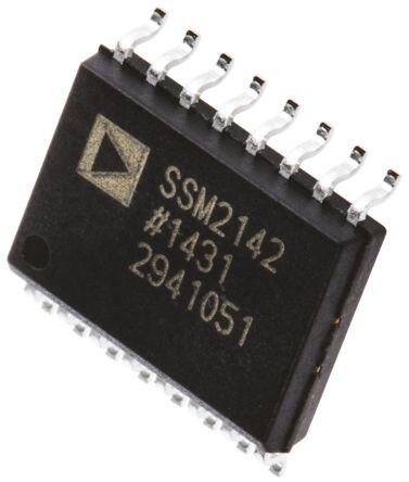
| 产品图片 |
|
| rohs | 符合RoHS无铅 / 符合限制有害物质指令(RoHS)规范要求 |
| 产品系列 | 放大器 IC,特殊用途放大器,Analog Devices SSM2142SZ- |
| 数据手册 | |
| 产品型号 | SSM2142SZ |
| 产品培训模块 | http://www.digikey.cn/PTM/IndividualPTM.page?site=cn&lang=zhs&ptm=30008http://www.digikey.cn/PTM/IndividualPTM.page?site=cn&lang=zhs&ptm=26202 |
| 产品目录页面 | |
| 产品种类 | 特殊用途放大器 |
| 供应商器件封装 | 16-SOIC W |
| 包装 | 管件 |
| 压摆率 | 15 V/µs |
| 可用增益调整 | 5.94 dB |
| 商标 | Analog Devices |
| 增益带宽积 | - |
| 安装类型 | 表面贴装 |
| 安装风格 | SMD/SMT |
| 封装 | Tube |
| 封装/外壳 | 16-SOIC(0.295",7.50mm 宽) |
| 封装/箱体 | SOIC-16 |
| 工作温度 | -40°C ~ 85°C |
| 工作电源电压 | 18 V |
| 工厂包装数量 | 47 |
| 放大器类型 | Cable Line Drivers |
| 最大双重电源电压 | +/- 18 V |
| 最大工作温度 | + 85 C |
| 最小工作温度 | - 40 C |
| 标准包装 | 47 |
| 电压-电源,单/双 (±) | ±13 V ~ 18 V |
| 电压-输入失调 | - |
| 电流-电源 | 5.5mA |
| 电流-输入偏置 | - |
| 电流-输出/通道 | 70mA |
| 电源电压-最大 | 18 V |
| 电源电压-最小 | - 18 V |
| 电源电流 | 5.5 mA |
| 电路数 | 1 |
| 类型 | Line Driver |
| 系列 | SSM2142 |
| 视频文件 | http://www.digikey.cn/classic/video.aspx?PlayerID=1364138032001&width=640&height=505&videoID=2245193153001http://www.digikey.cn/classic/video.aspx?PlayerID=1364138032001&width=640&height=505&videoID=2245193159001 |
| 输入电压范围—最大 | 18 V |
| 输出电流—典型值 | 70 mA |
| 输出类型 | Differential |
| 通道数量 | 1 Channel |


PDF Datasheet 数据手册内容提取
a Balanced Line Driver SSM2142 FEATURES FUNCTIONAL BLOCK DIAGRAM Transformer-Like Balanced Output Drives 10 V RMS Into a 600 (cid:86) Load VIN Stable When Driving Large Capacitive Loads and Long Cables 50W Low Distortion +OUT FORCE 0.006% typ 20 Hz–20 kHz, 10 V RMS into 600 (cid:86) High Slew Rate 15 V/(cid:109)s typ +OUT SENSE Low Gain Error 10kW – OUT SENSE (Differential or Single-Ended); 0.7% typ Outputs Short-Circuit Protected Available In Space-Saving 8-Pin Mini-DIP Package 50W Low Cost – OUT FORCE APPLICATIONS Audio Mix Consoles ALL RESISTORS 30kW Distribution Amplifiers UNLESS OTHERWISE 10kW Graphic and Parametric Equalizers INDICATED Dynamic Range Processors GND Digital Effects Processors Telecommunications Systems Industrial Instrumentation Hi-Fi Equipment GENERAL DESCRIPTION Based on a cross-coupled, electronically balanced topology, the The SSM2142 is an integrated differential-output buffer SSM2142 mimics the performance of fully balanced amplifier that converts a single-ended input signal to a balanced transformer-based solutions for line driving. However, the output signal pair with high output drive. By utilizing low noise SSM2142 maintains lower distortion and occupies much less thermally matched thin film resistors and high slew rate board space than transformers while achieving comparable amplifiers, the SSM2142 helps maintain the sonic quality of common-mode rejection performance with reduced parts count. audio systems by eliminating power line hum, RF interference, voltage drops, and other externally generated noise commonly The SSM2142 in tandem with the SSM2141 differential encountered with long audio cable runs. Excellent rejection of receiver establishes a complete, reliable solution for driving and common-mode noise and offset errors is achieved by laser receiving audio signals over long cables. The SSM2141 features trimming of the onboard resistors, assuring high gain accuracy. an Input Common-Mode Rejection Ratio of 100 dB at 60 Hz. The carefully designed output stage of the SSM2142 is capable Specifications demonstrating the performance of this typical of driving difficult loads, yielding low distortion performance system are included in the data sheet. despite extremely long cables or loads as low as 600 W , and is stable over a wide range of operating conditions. REV. C Information furnished by Analog Devices is believed to be accurate and reliable. However, no responsibility is assumed by Analog Devices for its use, nor for any infringements of patents or other rights of third parties which may result from its use. No license is granted by implication or otherwise under any patent or patent rights of Analog Devices.
SSM2142–SPECIFICATIONS (V = (cid:54)18 V, –40(cid:56)C £ T £ +85(cid:56)C, operating in differential mode unless otherwise S A noted. Typical characteristics apply to operation at T = +25(cid:56)C.) A Parameter Symbol Conditions Min Typ Max Units INPUT IMPEDANCE Z 10 kW IN INPUT CURRENT I V = – 7.071 V – 750 – 900 m A IN IN GAIN, DIFFERENTIAL 5.8 5.98 dB GAIN, SINGLE-ENDED Single-Ended Mode 5.7 5.94 dB GAIN ERROR, DIFFERENTIAL R = 600 W 0.7 2 % L POWER SUPPLY REJECTION RATIO STATIC PSRR V = – 13 V to – 18 V 60 80 dB S OUTPUT COMMON-MODE REJECTION OCMR See Test Circuit; f = 1 kHz –45 dB OUTPUT SIGNAL BALANCE RATIO SBR See Test Circuit; f = 1 kHz –40 dB TOTAL HARMONIC DISTORTION Plus Noise THD+N 20 Hz to 20 kHz, 0.006 % V = 10 V rms, R = 600 W O L SIGNAL-TO-NOISE RATIO SNR V = 0 V –93.4 dBu IN HEADROOM HR CLIP Level = 10.5 V rms +93.4 dBu SLEW RATE SR 15 V/m s OUTPUT COMMON-MODE VOLTAGE OFFSET1 V R = 600 W –250 25 250 mV OOS L DIFFERENTIAL OUTPUT VOLTAGE OFFSET V R = 600 W –50 15 50 mV OOD L DIFFERENTIAL OUTPUT VOLTAGE SWING V = – 7.071 V – 13.8 – 14.14 V IN OUTPUT IMPEDANCE Z 45 50 55 W O SUPPLY CURRENT I Unloaded, V = 0 V 5.5 7.0 mA SY IN OUTPUT CURRENT, SHORT CIRCUIT I 60 70 mA SC NOTES 1Output common-mode offset voltage can be removed by inserting dc blocking capacitors in the sense lines. See Applications Information. Specifications subject to change without notice. ABSOLUTE MAXIMUM RATINGS* PIN CONNECTIONS Supply Voltage . . . . . . . . . . . . . . . . . . . . . . . . . . . . . . . .– 18 V Storage Temperature . . . . . . . . . . . . . . . . . . –60(cid:176) C to +150(cid:176) C 8-Pin Plastic DIP 16-Pin Wide Body SOL Lead Temperature (Soldering, 60 sec) . . . . . . . . . . . . +300(cid:176) C (P Suffix) (S Suffix) Junction Temperature . . . . . . . . . . . . . . . . . . . . . . . . +150(cid:176) C Operating Temperature Range . . . . . . . . . . . . –40(cid:176) C to +85(cid:176) C NC 1 16 NC Output Short Circuit Duration (Both Outputs) . . . . Indefinite NC 2 15 NC *Stresses above those listed under “Absolute Maximum Ratings” may cause – FORCE 3 14 + FORCE permanent damage to the device. These are stress ratings only; the functional – SENSE 4 13 + SENSE operation of the device at these or any other conditions above those indicated in the GROUND 5 12 +V operational sections of this specification is not implied. Exposure to absolute maximum rating conditions for extended periods may affect device reliability. VIN 6 11 –V NC 7 10 NC NC 8 9 NC –2– REV. C
SSM2142 300W VOUT 300W V 1 8 300W 1 8 300W 2 7 2 7 3 6 +18V 600W 3 6 +18V 600W V VOUT VS= 0V 4 5 –18V VI N = 10V p–p 4 5 –18V VCMR= 10V p–p SBR = 20 LOG DV OUT OCMR = 20 LOG DV OUT VIN VCMR Figure 1.Output CMR Test Circuit Figure 2.Signal Balance Ratio (BBC Method) Test Circuit Typical Performance Characteristics 12 140 Bd – N 112000 DVVTAS S == = ±+ 1±2815VV°C srmV – G 108 TVRDASLIF===F .+6± M201508O°WVDCE IOT –PSR INW 0.1% DISTORTION CEEJ 80 SGE 6 0.01% DISTORTION RY 60 +PSR AT L L P O P V 4 SUR 40 UTP E T WPO 20 UO 2 0 0 10 100 1k 10k 100k 10 20 30 50 100 FREQUENCY – Hz FREQUENCY – kHz Figure 3.Power Supply Rejection vs. Frequency Figure 4.Maximum Output Voltage Swing vs. Frequency 12 6.5 ms 10 TRAL == +62050°WC 6.0 VTAIN== + 02V5°C r VG –N 8 FDRIFEFQ. .M =O 2D0EkHz Am – T 5.5 NO LOAD WI 0.1% DISTORTION NE S R E G 6 RU 5.0 A C T Y L L O P VT U 4 UPS 4.5 P T U O 2 4.0 0 3.5 ±2 ±6 ±10 ±14 ±18 ±2 ±6 ±10 ±14 ±18 SUPPLY VOLTAGE – Volts SUPPLY VOLTAGE – Volts Figure 5.Output Voltage Swing vs. Supply Voltage Figure 6.Supply Current vs. Supply Voltage REV. C –3–
SSM2142 THD PERFORMANCE The following data, taken from the THD test circuit on an Audio Precision System One using the internal 80 kHz noise filter, demonstrates the typical performance of a balanced pair system based on the SSM2142/SSM2141 chip set. Both dif- ferential and single-ended modes of operation are shown, under a number of output load conditions which simulate various application situations. Note also that there is no adverse effect on system performance when using the optional series feedback capacitors, which reject dc cable offsets in order to maintain optimal ac noise rejection. The large signal transient response of the system to a 100 kHz square wave input is also shown, demonstrating the stability of the SSM2142 under load. +18V A 10µF* C 4 6 Figure 9.THD+N vs. Frequency at Point B V 7 IN 3 S21S4M2 81 RL B S21S4M1 VOUT (Differential Mode) 2 5 10µF* R1 R2 –18V *USED ONLY IN THD PLOTS AS NOTED. ALL CABLE MEASUREMENTS USE BELDEN 8451 CABLE. Figure 7.THD Test Circuit Figure 10.THD+N vs. Frequency at Point A (Single Ended) Figure 8.THD+N vs. Frequency at Point B (Differential Mode) Figure 11.THD+N vs. Frequency at Point C (SSM2141 Output) –4– REV. C
SSM2142 on-chip 50 W series damping resistors. The impedances in the output buffer pair are precisely balanced by laser trimming during production. This results in the high gain accuracy needed to obtain good common-mode noise rejection, and 100 90 excellent separation between the offset error voltages common to the cable pair and the desired differential input signal. As shown in the test circuit, it is suggested that a suitable balanced, high input-impedance differential amplifier such as the SSM2141 be used at the receiving end for best system performance. The SSM2141 receiver output is configured for a gain of one half following the 6 dB gain of the SSM2142, in 10 order to maintain an overall system gain of unity. 0% In applications encountering a large dc offset on the cable or those wishing to ensure optimal rejection performance by avoiding differential offset error sources, dc blocking capacitors Figure 12.100 kHz Square Wave Observed at Point B may be employed at the sense outputs of the SSM2142. As (Differential Mode). V = 10 V rms, R1 = R2 = ¥ , R = 600 W shown in the test circuit, these components should present as O L little impedance as possible to minimize low-frequency errors, such as 10 m F NP (or tantalum if the polarity of the offset is known). SYSTEM GROUNDING CONSIDERATIONS Due to ground currents, supply variations, and other factors, 100 the ground potentials of the circuits at each end of a signal cable 90 may not be exactly equal. The primary purpose of a balanced pair line is to reject this voltage difference, commonly called “longitudinal error.” A measure of the ability of the system to reject longitudinal error voltage is output common-mode rejection. In order to obtain the optimal OCMR and noise rejection performance available with the SSM2142, the user 10 should observe the following precautions: 0% 1. The quality of the differential output is directly dependent upon the accuracy of the input voltage presented to the device. Input voltage errors developed across the impedance of the source must be avoided in order to maintain system Figure 13.100 kHz Square Wave at Point B (Differential Mode). V = 10 V rms, R1= R2 = ¥ , R = 600 W , with performance. The input of the SSM2142 should be driven O L directly by an operational amplifier or buffer offering low Series Feedback Capacitors source impedance and low noise. +15V 2. The ground input should be in close proximity to the single- +15V ended input’s source common. Ground offset errors encoun- tered in the source circuitry also impair system performance. VIN 4 SS6M 7 8 3 SS7M 5 6 VOUT 3. M0.1a kmeF s buyrep athssa tc athpea cSitSoMrs 2lo1c4a2t eisd acdloesqeu atote elya cdhe csouuppplleyd p wini.th 2141/ 3 2142 2 1 2 2143 1 4. Avoid the use of passive circuitry in series with the SSM2142 5 TWSIHSITEELDD-EPDAIR 4 outputs. Any reactive difference in the line pair will cause CABLE significant imbalances and affect the gain error of the device. –15V Snubber networks or series load resistors are not required to –15V maintain stability in SSM2142 based systems, even when driving signals over extremely long cables. Figure 14.Typical Application of the SSM2142 and SSM2141 5. Efforts should be made to maintain a physical balance in the arrangement of the signal pair wiring. Capacitive differences APPLICATIONS INFORMATION due to variations in routing or wire length may cause unequal The SSM2142 is designed to provide excellent common-mode noise pickup between the pair, which will degrade the system rejection, high output drive, and low signal distortion and noise OCMR. Shielded twisted-pair cable is the preferred choice in in a balanced line-driving system. The differential output stage all applications. The shield should not be utilized as a signal consists of twin cross-coupled unity gain buffer amplifiers with conductor. Grounding the shield at one end, near the output common, avoids ground loop currents flowing in the shield which increase noise coupling and longitudinal errors. REV. C –5–
SSM2142 THE CABLE PAIR The SSM2142 is capable of driving a 10 V rms signal into 600 W and will remain stable despite cable capacitances of up to 0.16 m F in either balanced or single-ended configurations. Low impedance shielded audio cable such as the standard Belden 8451 or similar is recommended, especially in applications traversing considerable distances. The user is cautioned that the so-called “audiophile” cables may incur four times the capac- itance per unit length of the standard industrial-grade product. In situations of extreme load and/or distance, adding a second parallel cable allows the user to trade off half of the total line resistance against a doubling in capacitive load. SINGLE-ENDED OPERATION The SSM2142 is designed to be compatible with existing balanced-pair interface systems. Just as in transformer-based circuits, identical but opposite currents are generated by the output pair which can be ground-referenced if desired and transmitted on a single wire. Single-ended operation requires that the unused side of the output pair be grounded to a solid return path in order to avoid voltage offset errors at the nearby input common. The signal quality obtained in these systems is directly dependent on the quality of the ground at each end of the wire. Also note that in single-ended operation the gain through the device is still 6 dB, and that the SSM2142 incurs no significant degradation in signal distortion or output drive capability, although the noise rejection inherent in balanced- pair systems is lost. POWER SUPPLY SEQUENCING A problem occasionally encountered in the interface system en- vironment involves irregular application of the supplies. The user is cautioned that applying power erratically can inadvert- ently bias parts of the circuit into a latch-up condition. The small geometries of an integrated circuit are easily breached and damaged by short-risetime spikes on a supply line, which usu- ally demonstrate considerable overshoot. The questionable practice of exchanging components or boards while under power can create such an undesirable sequence as well. Possible options which offer improved board-level device protection include: additional bypass capacitors, high-current reverse- biased steering diodes between both supplies and ground, vari- ous transient surge suppression devices, and safety grounding connectors. Likewise, power should be applied to the device before the output is connected to “live” systems which may carry voltages of sufficient magnitude to turn on the output devices of the A. SSM2142 and damage the device. In any case, of course, the U.S. user must always observe the absolute maximum ratings shown N in the specifications. D I E T N RI P –6– REV. C
SSM2142 OUTLINE DIMENSIONS 0.400 (10.16) 0.365 (9.27) 0.355 (9.02) 8 5 0.280 (7.11) 0.250 (6.35) 1 4 0.240 (6.10) 0.325 (8.26) 0.310 (7.87) 0.100 (2.54) 0.300 (7.62) BSC 0.060 (1.52) 0.195 (4.95) 0.210 (5.33) MAX 0.130 (3.30) MAX 0.115 (2.92) 0.015 0.150 (3.81) (0.38) 0.015 (0.38) 0.130 (3.30) MIN GAUGE 0.115 (2.92) SEATING PLANE 0.014 (0.36) PLANE 0.010 (0.25) 0.022 (0.56) 0.008 (0.20) 0.005 (0.13) 0.430 (10.92) 0.018 (0.46) MIN MAX 0.014 (0.36) 0.070 (1.78) 0.060 (1.52) 0.045 (1.14) COMPLIANTTO JEDEC STANDARDS MS-001 CONTROLLING DIMENSIONSARE IN INCHES; MILLIMETER DIMENSIONS (RCINOEFRPEANRREERENN LCTEEHA EODSNSEL MSY)AAAYNR BDEE AR CROOEU NNNFODIGETUDAR-POEPFDRFOA INSPC RWHIAH ETOEQL UFEIO VORAR LU EHSNAETL ISFN FLDOEEARSDIGSN.. 070606-A Figure 1. 8-Lead Plastic Dual In-Line Package [PDIP] Narrow Body (N-8) Dimensions shown in inches and (millimeters) 10.50(0.4134) 10.10(0.3976) 16 9 7.60(0.2992) 7.40(0.2913) 1 10.65(0.4193) 8 10.00(0.3937) 1.27(0.0500) 0.75(0.0295) BSC 2.65(0.1043) 0.25(0.0098) 45° 0.30(0.0118) 2.35(0.0925) 8° 0.10(0.0039) 0° COPLANARITY 0.10 0.51(0.0201) SPLEAATNIENG 0.33(0.0130) 1.27(0.0500) 0.31(0.0122) 0.20(0.0079) 0.40(0.0157) C(RINOEFNPEATRRREOENNLCLTEIHNCEOGOSNDMELISPYM)LAEAIANNRNDSETIAORTRNOOESUJNANEORDDETEEDAICN-POSMPFTRIFALONLMPIDMIRLAELIRATIMTDEEESRTFSMEO;SRIRN-0ECU1QH3SU-EADIVAIINMAELDENENSSTIIOGSNNFS.OR 03-27-2007-B Figure 2. 16-Lead Standard Small Outline Package [SOIC_W] Wide Body (RW-16) Dimensions shown in millimeters and (inches) ORDERING GUIDE Model1 Temperature Range Package Descriptions Package Option SSM2142PZ −40°C to +85°C 8-Lead PDIP N-8 SSM2142SZ −40°C to +85°C 16-Lead SOIC_W RW-16 SSM2142SZ-REEL −40°C to +85°C 16-Lead SOIC_W RW-16 1 Z = RoHS Compliant Part. Rev. C | Page 7 of 8
SSM2142 REVISION HISTORY 5/11—Rev. B to Rev. C Changes to Output Common-Mode Rejection Parameter and Output Signal Balance Ratio Parameter in SSM2142—Specifications Table ...................................................... 2 Updated Outline Dimensions ......................................................... 7 Changes to Ordering Guide ............................................................ 7 ©1991–2011 Analog Devices, Inc. All rights reserved. Trademarks and registered trademarks are the property of their respective owners. D01496-0-5/11(C) Rev. C | Page 8 of 8