ICGOO在线商城 > 集成电路(IC) > 线性 - 放大器 - 仪表,运算放大器,缓冲器放大器 > TL082IDRQ1

 Datasheet下载
- 型号: TL082IDRQ1
- 制造商: Texas Instruments
- 库位|库存: xxxx|xxxx
- 要求:
| 数量阶梯 | 香港交货 | 国内含税 |
| +xxxx | $xxxx | ¥xxxx |
查看当月历史价格
查看今年历史价格
TL082IDRQ1产品简介:
ICGOO电子元器件商城为您提供TL082IDRQ1由Texas Instruments设计生产,在icgoo商城现货销售,并且可以通过原厂、代理商等渠道进行代购。 TL082IDRQ1价格参考。Texas InstrumentsTL082IDRQ1封装/规格:线性 - 放大器 - 仪表,运算放大器,缓冲器放大器, J-FET Amplifier 2 Circuit 8-SOIC。您可以下载TL082IDRQ1参考资料、Datasheet数据手册功能说明书,资料中有TL082IDRQ1 详细功能的应用电路图电压和使用方法及教程。
TL082IDRQ1是Texas Instruments推出的一款双通道JFET输入运算放大器,符合汽车级标准(AEC-Q100认证),适用于严苛的工业与汽车环境。其主要应用场景包括:

在汽车电子系统中,常用于车载传感器信号调理,如温度、压力和位置传感器的放大与处理,得益于其低功耗、宽工作温度范围(-40°C 至 125°C)及高可靠性。此外,在电机控制、电池管理系统(BMS)和车载音频前置放大电路中也广泛应用。

在工业领域,TL082IDRQ1适用于数据采集系统、有源滤波器、模拟信号缓冲和电压跟随器等电路,凭借高输入阻抗、低输入偏置电流和低噪声特性,可有效提升信号完整性。其单位增益稳定设计使其在非反相和反相放大配置中均表现良好。

该器件还常用于电源管理电路中的误差放大器,以及需要高精度模拟处理的仪器仪表中。其D封装(SOIC)便于表面贴装,适合自动化生产。

总之,TL082IDRQ1凭借高性价比、优良的动态性能和车规级可靠性,广泛应用于汽车电子、工业控制、测量设备和通用模拟信号处理等场景。
| 参数 | 数值 |
| -3db带宽 | - |
| 产品目录 | 集成电路 (IC)半导体 |
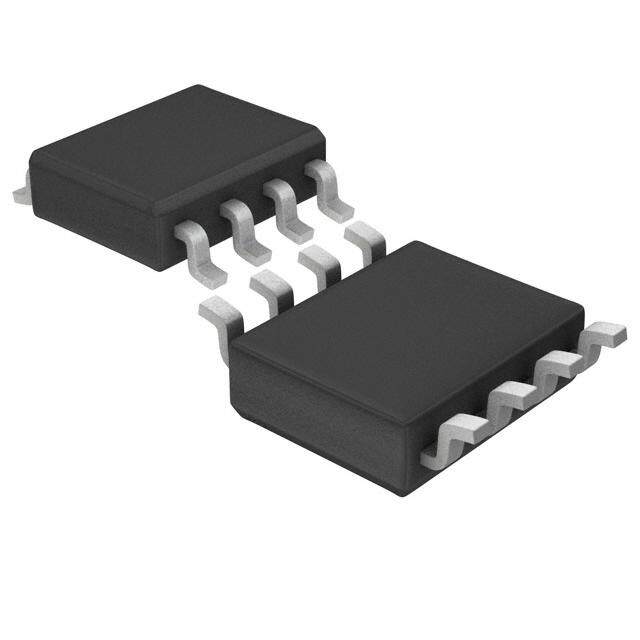
| 描述 | IC OPAMP JFET 3MHZ DUAL 8SOIC运算放大器 - 运放 JFET-Inp Op Amp |
| 产品分类 | Linear - Amplifiers - Instrumentation, OP Amps, Buffer Amps集成电路 - IC |
| 品牌 | Texas Instruments |
| 产品手册 | |
| 产品图片 |
|
| rohs | 符合RoHS无铅 / 符合限制有害物质指令(RoHS)规范要求 |
| 产品系列 | 放大器 IC,运算放大器 - 运放,Texas Instruments TL082IDRQ1自动,AEC-Q100 |
| 数据手册 | |
| 产品型号 | TL082IDRQ1 |
| 产品种类 | 运算放大器 - 运放 |
| 供应商器件封装 | 8-SOIC |
| 共模抑制比—最小值 | 75 dB |
| 关闭 | No Shutdown |
| 其它名称 | 296-36981-6 |
| 包装 | Digi-Reel® |
| 单位重量 | 72.600 mg |
| 单电源电压 | 7 V to 36 V |
| 压摆率 | 13 V/µs |
| 双重电源电压 | +/- 5 V, +/- 9 V, +/- 12 V, +/- 15 V |
| 商标 | Texas Instruments |
| 增益带宽生成 | 3 MHz |
| 增益带宽积 | 3MHz |
| 安装类型 | 表面贴装 |
| 安装风格 | SMD/SMT |
| 封装 | Reel |
| 封装/外壳 | 8-SOIC(0.154",3.90mm 宽) |
| 封装/箱体 | SOIC-8 |
| 工作温度 | -40°C ~ 85°C |
| 工作电源电压 | 7 V to 36 V, +/- 3.5 V to +/- 18 V |
| 工厂包装数量 | 2500 |
| 技术 | BiFET |
| 放大器类型 | J-FET |
| 最大双重电源电压 | +/- 18 V |
| 最大工作温度 | + 85 C |
| 最小双重电源电压 | +/- 3.5 V |
| 最小工作温度 | - 40 C |
| 标准包装 | 1 |
| 电压-电源,单/双 (±) | 7 V ~ 36 V, ±3.5 V ~ 18 V |
| 电压-输入失调 | 3mV |
| 电流-电源 | 1.4mA |
| 电流-输入偏置 | 30pA |
| 电流-输出/通道 | - |
| 电源电流 | 5.6 mA |
| 电路数 | 2 |
| 系列 | TL082-Q1 |
| 转换速度 | 13 V/us |
| 输入偏压电流—最大 | 200 pA |
| 输入参考电压噪声 | 18 nV |
| 输入补偿电压 | 6 mV |
| 输出类型 | - |
| 通道数量 | 2 Channel |


- 商务部:美国ITC正式对集成电路等产品启动337调查
- 曝三星4nm工艺存在良率问题 高通将骁龙8 Gen1或转产台积电
- 太阳诱电将投资9.5亿元在常州建新厂生产MLCC 预计2023年完工
- 英特尔发布欧洲新工厂建设计划 深化IDM 2.0 战略
- 台积电先进制程称霸业界 有大客户加持明年业绩稳了
- 达到5530亿美元!SIA预计今年全球半导体销售额将创下新高
- 英特尔拟将自动驾驶子公司Mobileye上市 估值或超500亿美元
- 三星加码芯片和SET,合并消费电子和移动部门,撤换高东真等 CEO
- 三星电子宣布重大人事变动 还合并消费电子和移动部门
- 海关总署:前11个月进口集成电路产品价值2.52万亿元 增长14.8%


PDF Datasheet 数据手册内容提取
TL082-Q1 JFET-INPUT OPERATIONAL AMPLIFIER www.ti.com SLOS548–SEPTEMBER2007 FEATURES 1 D PACKAGE • QualifiedforAutomotiveApplications (TOPVIEW) • LowPowerConsumption • WideCommon-ModeandDifferential 1OUT 1 8 VCC+ 1IN– 2 7 2OUT VoltageRanges 1IN+ 3 6 2IN– • LowInputBiasandOffsetCurrents VCC– 4 5 2IN+ • LowTotalHarmonicDistortion:0.003%Typ • HighInputImpedance:JFET-InputStage • Latchup-FreeOperation • HighSlewRate:13V/μsTyp • Common-ModeInputVoltageRange IncludesV CC+ DESCRIPTION/ORDERING INFORMATION The TL082 JFET-input operational amplifier incorporates well-matched, high-voltage JFET and bipolar transistors in a monolithic integrated circuit. The device features high slew rates, low input bias and offset currents, and low offset-voltagetemperaturecoefficient. The I-suffix device is characterized for operation from –40(cid:176) C to 85(cid:176) C. The Q-suffix device is characterized for operationfrom–40(cid:176) Cto125(cid:176) C. ORDERINGINFORMATION(1) T PACKAGE(2) ORDERABLEPARTNUMBER TOP-SIDEMARKING J –40(cid:176) Cto85(cid:176) C SOIC–D Reelof2500 TL082IDRQ1 TL082I –40(cid:176) Cto125(cid:176) C SOIC–D Reelof2500 TL082QDRQ1 TL082Q (1) Forthemostcurrentpackageandorderinginformation,seethePackageOptionAddendumattheendofthisdocument,orseetheTI websiteatwww.ti.com. (2) Packagedrawings,thermaldata,andsymbolizationareavailableatwww.ti.com/packaging. 1 Pleasebeawarethatanimportantnoticeconcerningavailability,standardwarranty,anduseincriticalapplicationsof TexasInstrumentssemiconductorproductsanddisclaimerstheretoappearsattheendofthisdatasheet. PRODUCTIONDATAinformationiscurrentasofpublicationdate. Copyright©2007,TexasInstrumentsIncorporated Products conform to specifications per the terms of the Texas Instruments standard warranty. Production processing does not necessarilyincludetestingofallparameters.
TL082-Q1 JFET-INPUT OPERATIONAL AMPLIFIER www.ti.com SLOS548–SEPTEMBER2007 SYMBOL(EACHAMPLIFIER) IN+ + OUT IN– - SCHEMATIC(EACHAMPLIFIER) V CC+ IN+ 64W IN– OUT 128W 64W C1 1080W 1080W V CC– A. Componentvaluesshownarenominal. 2 SubmitDocumentationFeedback Copyright©2007,TexasInstrumentsIncorporated
TL082-Q1 JFET-INPUT OPERATIONAL AMPLIFIER www.ti.com SLOS548–SEPTEMBER2007 ABSOLUTE MAXIMUM RATINGS(1) overoperatingfree-airtemperaturerange(unlessotherwisenoted) VALUE V Supplyvoltage,positive(2) 18V CC+ V Supplyvoltage,negative(2) –18V CC– V Differentialinputvoltage(3) ±30V ID V Inputvoltage(2)(4) ±15V I Durationofoutputshortcircuit(5) Unlimited Continuoustotalpowerdissipation (6) TL082I –40(cid:176) Cto85(cid:176) C T Operatingfree-airtemperaturerange A TL082Q –40(cid:176) Cto125(cid:176) C θ Packagethermalimpedance,junctiontofreeair(7) 97(cid:176) C/W JA Human-BodyModel 1.5kV(H1C) ESDrating(8) Charged-DeviceModel 1.5kV(C5) MachineModel 200V(M3) Operatingvirtualjunctiontemperature 150(cid:176) C T Storagetemperaturerange –65(cid:176) Cto150(cid:176) C stg (1) Stressesbeyondthoselistedunder"absolutemaximumratings"maycausepermanentdamagetothedevice.Thesearestressratings only,andfunctionaloperationofthedeviceattheseoranyotherconditionsbeyondthoseindicatedunder"recommendedoperating conditions"isnotimplied.Exposuretoabsolute-maximum-ratedconditionsforextendedperiodsmayaffectdevicereliability. (2) Allvoltagevalues,exceptdifferentialvoltages,arewithrespecttothemidpointbetweenV andV . CC+ CC– (3) DifferentialvoltagesareatIN+withrespecttoIN–. (4) Themagnitudeoftheinputvoltagemustneverexceedthemagnitudeofthesupplyvoltageor15V,whicheverisless. (5) Theoutputmaybeshortedtogroundortoeithersupply.Temperatureand/orsupplyvoltagesmustbelimitedtoensurethatthe dissipationratingisnotexceeded. (6) MaximumpowerdissipationisafunctionofT(max),θ ,andT .Themaximumallowablepowerdissipationatanyallowableambient J JA A temperatureisPD=(T(max)–T )/θ .OperatingattheabsolutemaximumT of150(cid:176) Ccanaffectreliability. J A JA J (7) ThepackagethermalimpedanceiscalculatedinaccordancewithJESD51-7. (8) ESDprotectionlevelperJEDECclassificationsJESD22-A114(HBM),JESD22-A115(MM),andJESD22-C101(CDM). Copyright©2007,TexasInstrumentsIncorporated SubmitDocumentationFeedback 3
TL082-Q1 JFET-INPUT OPERATIONAL AMPLIFIER www.ti.com SLOS548–SEPTEMBER2007 ELECTRICAL CHARACTERISTICS(1) V =±15V(unlessotherwisenoted) CC± PARAMETER TESTCONDITIONS T (2) MIN TYP MAX UNIT A 25(cid:176) C 3 6 V Inputoffsetvoltage V =0,R =50Ω mV IO O S Fullrange 9 α Temperaturecoefficientofinput V =0,R =50Ω Fullrange 18 μV/(cid:176) C VIO offsetvoltage O S 25(cid:176) C 5 100 pA I Inputoffsetcurrent(3) V =0 IO O Fullrange 20 nA 25(cid:176) C 30 200 pA I Inputbiascurrent(3) V =0 IB O Fullrange 50 nA V Common-modeinput 25(cid:176) C ±11 –12 V ICR voltagerange to15 R =10kΩ 25(cid:176) C ±12 ±13.5 L Maximumpeakoutput V R ≥10kΩ ±12 V OM voltageswing L Fullrange R ≥2kΩ ±10 ±12 L Large-signaldifferentialvoltage 25(cid:176) C 50 200 A V =±10V,R ≥2kΩ V/mV VD amplification O L Fullrange 15 B1 Unity-gainbandwidth 25(cid:176) C 3 MHz r Inputresistance 25(cid:176) C 1012 Ω i CMRR Common-moderejectionratio V =V (min),V =0,R =50Ω 25(cid:176) C 75 86 dB IC ICR O S k Supply-voltagerejectionratio VCC=±15Vto±9V, 25(cid:176) C 80 86 dB SVR (ΔV /ΔV ) V =0,R =50Ω CC± IO O S I Supplycurrent(peramplifier) V =0,Noload 25(cid:176) C 1.4 2.8 mA CC O V /V Crosstalkattenuation A =100 25(cid:176) C 120 dB O1 O2 VD (1) Allcharacteristicsaremeasuredunderopen-loopconditionswithzerocommon-modevoltage,unlessotherwisespecified. (2) FullrangeforT is–40(cid:176) Cto85(cid:176) CforI-suffixdevicesand–40(cid:176) Cto125(cid:176) CforQ-suffixdevices. A (3) InputbiascurrentsofanFET-inputoperationalamplifierarenormaljunctionreversecurrents,whicharetemperaturesensitive,as showninFigure14.Pulsetechniquesmustbeusedthatmaintainthejunctiontemperatureasclosetotheambienttemperatureas possible. OPERATING CHARACTERISTICS V =±15V,T =25(cid:176) C(unlessotherwisenoted) CC± A PARAMETER TESTCONDITIONS MIN TYP MAX UNIT SR Slewrateatunitygain V =10V,R =2kΩ,C =100pF,SeeFigure1 8 13 V/μs I L L t Risetime V =20mV,R =2kΩ,C =100pF,SeeFigure1 0.05 μs r I L L Overshootfactor V =20mV,R =2kΩ,C =100pF,SeeFigure1 20 % I L L f=1kHz 18 nV/√Hz V Equivalentinputnoisevoltage R =20Ω n S f=10Hzto10kHz 4 μV I Equivalentinputnoisecurrent R =20Ω,f=1kHz 0.01 pA/√Hz n S THD Totalharmonicdistortion V =6V,f=1kHz,AVD=1,R ≤1kΩ,R ≥2kΩ 0.003 % Irms S L 4 SubmitDocumentationFeedback Copyright©2007,TexasInstrumentsIncorporated
TL082-Q1 JFET-INPUT OPERATIONAL AMPLIFIER www.ti.com SLOS548–SEPTEMBER2007 PARAMETER MEASUREMENT INFORMATION - OUT VI + CL= 100 pF RL= 2 kW Figure1. 10 kW 1 kW VI - OUT + RL CL= 100 pF Figure2. Copyright©2007,TexasInstrumentsIncorporated SubmitDocumentationFeedback 5
TL082-Q1 JFET-INPUT OPERATIONAL AMPLIFIER www.ti.com SLOS548–SEPTEMBER2007 TYPICAL CHARACTERISTICS Dataathighandlowtemperaturesareapplicableonlywithintheratedoperatingfree-airtemperaturerangesofthedevices. TableofGraphs FIGURE vsFrequency 3,4,5 vsFree-airtemperature 6 V Maximumpeakoutputvoltage OM vsLoadresistance 7 vsSupplyvoltage 8 vsFree-airtemperature 9 A Large-signaldifferentialvoltageamplification VD vsFrequency 10 P Totalpowerdissipation vsFree-airtemperature 11 D vsFree-airtemperature 12 I Supplycurrent CC vsSupplyvoltage 13 I Inputbiascurrent vsFree-airtemperature 14 IB Large-signalpulseresponse vsTime 15 V Outputvoltage vsElapsedtime 16 O CMRR Common-moderejectionratio vsFree-airtemperature 17 V Equivalentinputnoisevoltage vsFrequency 18 n THD Totalharmonicdistortion vsFrequency 19 MAXIMUMPEAKOUTPUTVOLTAGE MAXIMUMPEAKOUTPUTVOLTAGE vs vs FREQUENCY FREQUENCY (SeeFigure2) (SeeFigure2) ±15 ±15 ge -V ±12.5 VCC±=±15V RTAL== 2150° CkΩ e -V ±12.5 VCC±=±15V RTAL== 225 k°ΩC a g oltputV ±10 VCC±=±10V oltautV ±10 Out utp VCC±=±10V ak ±7.5 k O ±7.5 e a P e m P mu ±5 VCC±=±5V um ±5 axi xim VCC±=±5V M a - M ±2.5 - M ±2.5 O M V O V 0 0 100 1k 10k 100k 1M 10M 100 1k 10k 100k 1M 10M f - Frequency - Hz f - Frequency - Hz Figure3. Figure4. 6 SubmitDocumentationFeedback Copyright©2007,TexasInstrumentsIncorporated
TL082-Q1 JFET-INPUT OPERATIONAL AMPLIFIER www.ti.com SLOS548–SEPTEMBER2007 MAXIMUMPEAKOUTPUTVOLTAGE MAXIMUMPEAKOUTPUTVOLTAGE vs vs FREQUENCY FREE-AIRTEMPERATURE (SeeFigure2) (SeeFigure2) ±15 ±15 VCC±=±15V V RL= 10 kW e -V ±12.5 TA= 25°C RL= 2 kΩ ge - ±12.5 oltag oltaV RL= 2 kW utputV ±10 TA= -55°C Output ±10 k O ±7.5 ak ±7.5 a e e P um P ±5 TA= 125°C mum ±5 m xi axi a M M - ±2.5 - M ±2.5 OM VO VCC±=±15V V 0 0 10k 40k 100k 400k 1M 4M 10M -75 -50 -25 0 25 50 75 100 125 f - Frequency - Hz TA- Free-Air Temperature -°C Figure5. Figure6. MAXIMUMPEAKOUTPUTVOLTAGE vs MAXIMUMPEAKOUTPUTVOLTAGE LOADRESISTANCE vs (SeeFigure2) SUPPLYVOLTAGE ±15 ±15 V VCC±=±15V RL= 10 kΩ ge - ±12.5 TA= 25°C e -V ±12.5 TA= 25°C a g oltV olta put ±10 utV ±10 Out utp ak k O e ±7.5 a ±7.5 P e um m P m u axi ±5 xim ±5 M a - M - M O ±2.5 M ±2.5 V O V 0 0 0.1 0.2 0.4 0.7 1 2 4 7 10 0 2 4 6 8 10 12 14 16 RL- Load Resistance - k Ω |VCC±| - SupplyVoltage - V Figure7. Figure8. Copyright©2007,TexasInstrumentsIncorporated SubmitDocumentationFeedback 7
TL082-Q1 JFET-INPUT OPERATIONAL AMPLIFIER www.ti.com SLOS548–SEPTEMBER2007 LARGE-SIGNALDIFFERENTIALVOLTAGEAMPLIFICATION LARGE-SIGNALDIFFERENTIALVOLTAGEAMPLIFICATION vs vs FREE-AIRTEMPERATURE FREQUENCY 1000 106 700 VCC±=±5V to±15V RL= 10 kΩ 400 105 TA= 25°C erential V/mV 200 erential V/mV 104 0° - Large-Signal DiffAVDVAoltagemplification - 171240700000 A- gLare-Signal DiffVDVoltAmpagelification - 111000321 (Prihgahste s Scahlieft) DiffAe(mrleepnftlti ifsaicclaaVltoeiol)tnage 1943055°°°Phase Shift 4 VCC±=±15V VO=±10V 2 RL= 2 kΩ 1 180° 1 10 100 1k 10k 100k 1M 10M 1 -75 -50 -25 0 25 50 75 100 125 f - Frequency - Hz TA- Free-Air Temperature -°C Figure9. Figure10. POWERDISSIPATION SUPPLYCURRENT vs vs FREE-AIRTEMPERATURE FREE-AIRTEMPERATURE 250 2.0 VCC±=±15V VCC±=±15V 225 No Signal 1.8 No Signal No Load No Load 200 1.6 W A m m on - 175 nt – 1.4 pati 150 urre 1.2 si C Dis 125 ply 1.0 r p we 100 Su 0.8 Po – otal 75 CC± 0.6 T 50 I 0.4 - D P 25 0.2 0 0 -75 -50 -25 0 25 50 75 100 125 –75 –50 –25 0 25 50 75 100 125 TA- Free-Air Temperature -°C TA– Free-AirTemperature – °C Figure11. Figure12. 8 SubmitDocumentationFeedback Copyright©2007,TexasInstrumentsIncorporated
TL082-Q1 JFET-INPUT OPERATIONAL AMPLIFIER www.ti.com SLOS548–SEPTEMBER2007 SUPPLYCURRENT INPUTBIASCURRENT vs vs SUPPLYVOLTAGE FREE-AIRTEMPERATURE 2.0 100 1.8 TA= 25°C VCC±=±15V No Signal No Load 1.6 A A 10 m n nt - 1.4 ent - rre 1.2 urr u C y C 1.0 as 1 pl Bi up 0.8 ut S p - ± 0.6 - In ICC 0.4 IIB 0.1 0.2 0 0.01 0 2 4 6 8 10 12 14 16 - 50 - 25 0 25 50 75 100 125 |VCC±| - SupplyVoltage - V TA- Free-Air Temperature -°C Figure13. Figure14. OUTPUTVOLTAGE vs ELAPSEDTIME VOLTAGE-FOLLOWERLARGE-SIGNALPULSERESPONSE (SeeFigure1) 6 VCC±=±15V 28 RL= 2 kΩ CL= 100 pF 24 V 4 TA= 25°C s - Output V 20 e m oltagV 2 age - 16 VCC±=±15V ut olt RL= 2 kΩ ut and Outp - 20 - OutputVO 128 CTAL== 2150°0C pF np Input V 4 I - 4 0 - 6 - 4 0 0.5 1 1.5 2 2.5 3 3.5 0 0.2 0.4 0.6 0.8 1.0 1.2 t - Time - µs t - Elapsed Time - µs Figure15. Figure16. Copyright©2007,TexasInstrumentsIncorporated SubmitDocumentationFeedback 9
TL082-Q1 JFET-INPUT OPERATIONAL AMPLIFIER www.ti.com SLOS548–SEPTEMBER2007 COMMON-MODEREJECTIONRATIO EQUIVALENTINPUTNOISEVOLTAGE vs vs FREE-AIRTEMPERATURE FREQUENCY 89 50 VCC±=±15V Hz VCC±=±15V dB RL= 10 kΩ AVD= 10 Ratio – 88 e nV/- 40 RTAS== 2250°CΩ ction 87 oltagV eje se 30 R oi e 86 N od ut M p mon- 85 ent In 20 m al o v R – C 84 Equil 10 R - M n C V 83 0 –75 –50 –25 0 25 50 75 100 125 10 40 100 400 1 k 4 k 10 k 40 k 100 k TA– Free-AirTemperature – °C f - Frequency - Hz Figure17. Figure18. TOTALHARMONICDISTORTION vs FREQUENCY 1 VCC±=±15V 0.4 AVD= 1 % VI(RMS)= 6V n - TA= 25°C o rti 0.1 o st Di c 0.04 ni o m r a H al 0.01 ot T D - 0.004 H T 0.001 10 400 1k 4k 10k 40k 100k f - Frequency - Hz Figure19. 10 SubmitDocumentationFeedback Copyright©2007,TexasInstrumentsIncorporated
TL082-Q1 JFET-INPUT OPERATIONAL AMPLIFIER www.ti.com SLOS548–SEPTEMBER2007 APPLICATION INFORMATION RF= 100 kW 15V 3.3 kW Output - 1/2 TL082 CF= 3.3 µF + 1 kW –15V 3.3 kW 9.1 kW 1 f = 2pR C F F Figure20. VCC+ - 1/2 R1 R2 TL082 Input + Output C3 VCC– R3 R1 = R2 = 2(R3) = 1.5 MW C1 C2 C3 C1 = C2 = = 110 pF 2 1 fo= 2pR1 C1 = 1 kHz Figure21. VCC+ 1 MΩ - TL082 Output A VCC+ + + 1 µF TL082 VCC+ Input - - TL082 Output B 100 kΩ 100 kΩ + VCC+ 100 kΩ 100 µF 100 kΩ VCC+ - TL082 Output C + Figure22.Audio-DistributionAmplifier Copyright©2007,TexasInstrumentsIncorporated SubmitDocumentationFeedback 11
TL082-Q1 JFET-INPUT OPERATIONAL AMPLIFIER www.ti.com SLOS548–SEPTEMBER2007 6 sinωt 1N4148 - 15 V 18 pF 18 kΩ 1 kΩ (see Note A) 18 pF VCC+ -1/2 88.4 kΩ VCC+ - TL082 1/2 88.4 kΩ + TL082 6 cosωt VCC- + 18 pF VCC- 1 kΩ 15V 1N4148 18 kΩ 88.4 kΩ (see Note A) A. Theseresistorvaluesmaybeadjustedforasymmetricaloutput. Figure23.100-kHzQuadratureOscillator 16 kΩ 16 kΩ 220 pF 220 pF 43 kΩ 30 kΩ 43 kΩ 30 kΩ 43 kΩ VCC+ VCC+ 220 pF VCC+ 220 pF VCC+ Input 1-/2 43 kΩ - 43 kΩ 1-/2 43 kΩ - TL082 1/2 TL082 1/2 Output + TL082 + TL082 B + + 1.5 kΩ VCC- 1.5 kΩ VCC- VCC- VCC- Output A Output A Output B 2 kHz/div 2 kHz/div Second-Order Bandpass Filter Cascaded Bandpass Filter fo= 100 kHz,Q = 30,GAIN = 4 fo= 100 kHz,Q = 69,GAIN = 16 Figure24.Positive-FeedbackBandpassFilter 12 SubmitDocumentationFeedback Copyright©2007,TexasInstrumentsIncorporated
PACKAGE OPTION ADDENDUM www.ti.com 6-Feb-2020 PACKAGING INFORMATION Orderable Device Status Package Type Package Pins Package Eco Plan Lead/Ball Finish MSL Peak Temp Op Temp (°C) Device Marking Samples (1) Drawing Qty (2) (6) (3) (4/5) TL082IDRQ1 ACTIVE SOIC D 8 2500 Green (RoHS NIPDAU Level-1-260C-UNLIM -40 to 85 TL082I & no Sb/Br) TL082QDRQ1 ACTIVE SOIC D 8 2500 Green (RoHS NIPDAU Level-1-260C-UNLIM -40 to 125 TL082Q & no Sb/Br) (1) The marketing status values are defined as follows: ACTIVE: Product device recommended for new designs. LIFEBUY: TI has announced that the device will be discontinued, and a lifetime-buy period is in effect. NRND: Not recommended for new designs. Device is in production to support existing customers, but TI does not recommend using this part in a new design. PREVIEW: Device has been announced but is not in production. Samples may or may not be available. OBSOLETE: TI has discontinued the production of the device. (2) RoHS: TI defines "RoHS" to mean semiconductor products that are compliant with the current EU RoHS requirements for all 10 RoHS substances, including the requirement that RoHS substance do not exceed 0.1% by weight in homogeneous materials. Where designed to be soldered at high temperatures, "RoHS" products are suitable for use in specified lead-free processes. TI may reference these types of products as "Pb-Free". RoHS Exempt: TI defines "RoHS Exempt" to mean products that contain lead but are compliant with EU RoHS pursuant to a specific EU RoHS exemption. Green: TI defines "Green" to mean the content of Chlorine (Cl) and Bromine (Br) based flame retardants meet JS709B low halogen requirements of <=1000ppm threshold. Antimony trioxide based flame retardants must also meet the <=1000ppm threshold requirement. (3) MSL, Peak Temp. - The Moisture Sensitivity Level rating according to the JEDEC industry standard classifications, and peak solder temperature. (4) There may be additional marking, which relates to the logo, the lot trace code information, or the environmental category on the device. (5) Multiple Device Markings will be inside parentheses. Only one Device Marking contained in parentheses and separated by a "~" will appear on a device. If a line is indented then it is a continuation of the previous line and the two combined represent the entire Device Marking for that device. (6) Lead/Ball Finish - Orderable Devices may have multiple material finish options. Finish options are separated by a vertical ruled line. Lead/Ball Finish values may wrap to two lines if the finish value exceeds the maximum column width. Important Information and Disclaimer:The information provided on this page represents TI's knowledge and belief as of the date that it is provided. TI bases its knowledge and belief on information provided by third parties, and makes no representation or warranty as to the accuracy of such information. Efforts are underway to better integrate information from third parties. TI has taken and continues to take reasonable steps to provide representative and accurate information but may not have conducted destructive testing or chemical analysis on incoming materials and chemicals. TI and TI suppliers consider certain information to be proprietary, and thus CAS numbers and other limited information may not be available for release. In no event shall TI's liability arising out of such information exceed the total purchase price of the TI part(s) at issue in this document sold by TI to Customer on an annual basis. Addendum-Page 1
PACKAGE OPTION ADDENDUM www.ti.com 6-Feb-2020 OTHER QUALIFIED VERSIONS OF TL082-Q1 : •Catalog: TL082 •Military: TL082M NOTE: Qualified Version Definitions: •Catalog - TI's standard catalog product •Military - QML certified for Military and Defense Applications Addendum-Page 2
PACKAGE OUTLINE D0008A SOIC - 1.75 mm max height SCALE 2.800 SMALL OUTLINE INTEGRATED CIRCUIT C SEATING PLANE .228-.244 TYP [5.80-6.19] .004 [0.1] C A PIN 1 ID AREA 6X .050 [1.27] 8 1 2X .189-.197 [4.81-5.00] .150 NOTE 3 [3.81] 4X (0 -15 ) 4 5 8X .012-.020 B .150-.157 [0.31-0.51] .069 MAX [3.81-3.98] .010 [0.25] C A B [1.75] NOTE 4 .005-.010 TYP [0.13-0.25] 4X (0 -15 ) SEE DETAIL A .010 [0.25] .004-.010 0 - 8 [0.11-0.25] .016-.050 [0.41-1.27] DETAIL A (.041) TYPICAL [1.04] 4214825/C 02/2019 NOTES: 1. Linear dimensions are in inches [millimeters]. Dimensions in parenthesis are for reference only. Controlling dimensions are in inches. Dimensioning and tolerancing per ASME Y14.5M. 2. This drawing is subject to change without notice. 3. This dimension does not include mold flash, protrusions, or gate burrs. Mold flash, protrusions, or gate burrs shall not exceed .006 [0.15] per side. 4. This dimension does not include interlead flash. 5. Reference JEDEC registration MS-012, variation AA. www.ti.com
EXAMPLE BOARD LAYOUT D0008A SOIC - 1.75 mm max height SMALL OUTLINE INTEGRATED CIRCUIT 8X (.061 ) [1.55] SYMM SEE DETAILS 1 8 8X (.024) [0.6] SYMM (R.002 ) TYP [0.05] 5 4 6X (.050 ) [1.27] (.213) [5.4] LAND PATTERN EXAMPLE EXPOSED METAL SHOWN SCALE:8X SOLDER MASK SOLDER MASK METAL OPENING OPENING METAL UNDER SOLDER MASK EXPOSED METAL EXPOSED METAL .0028 MAX .0028 MIN [0.07] [0.07] ALL AROUND ALL AROUND NON SOLDER MASK SOLDER MASK DEFINED DEFINED SOLDER MASK DETAILS 4214825/C 02/2019 NOTES: (continued) 6. Publication IPC-7351 may have alternate designs. 7. Solder mask tolerances between and around signal pads can vary based on board fabrication site. www.ti.com
EXAMPLE STENCIL DESIGN D0008A SOIC - 1.75 mm max height SMALL OUTLINE INTEGRATED CIRCUIT 8X (.061 ) [1.55] SYMM 1 8 8X (.024) [0.6] SYMM (R.002 ) TYP [0.05] 5 4 6X (.050 ) [1.27] (.213) [5.4] SOLDER PASTE EXAMPLE BASED ON .005 INCH [0.125 MM] THICK STENCIL SCALE:8X 4214825/C 02/2019 NOTES: (continued) 8. Laser cutting apertures with trapezoidal walls and rounded corners may offer better paste release. IPC-7525 may have alternate design recommendations. 9. Board assembly site may have different recommendations for stencil design. www.ti.com
IMPORTANTNOTICEANDDISCLAIMER TI PROVIDES TECHNICAL AND RELIABILITY DATA (INCLUDING DATASHEETS), DESIGN RESOURCES (INCLUDING REFERENCE DESIGNS), APPLICATION OR OTHER DESIGN ADVICE, WEB TOOLS, SAFETY INFORMATION, AND OTHER RESOURCES “AS IS” AND WITH ALL FAULTS, AND DISCLAIMS ALL WARRANTIES, EXPRESS AND IMPLIED, INCLUDING WITHOUT LIMITATION ANY IMPLIED WARRANTIES OF MERCHANTABILITY, FITNESS FOR A PARTICULAR PURPOSE OR NON-INFRINGEMENT OF THIRD PARTY INTELLECTUAL PROPERTY RIGHTS. These resources are intended for skilled developers designing with TI products. You are solely responsible for (1) selecting the appropriate TI products for your application, (2) designing, validating and testing your application, and (3) ensuring your application meets applicable standards, and any other safety, security, or other requirements. These resources are subject to change without notice. TI grants you permission to use these resources only for development of an application that uses the TI products described in the resource. Other reproduction and display of these resources is prohibited. No license is granted to any other TI intellectual property right or to any third party intellectual property right. TI disclaims responsibility for, and you will fully indemnify TI and its representatives against, any claims, damages, costs, losses, and liabilities arising out of your use of these resources. TI’s products are provided subject to TI’s Terms of Sale (www.ti.com/legal/termsofsale.html) or other applicable terms available either on ti.com or provided in conjunction with such TI products. TI’s provision of these resources does not expand or otherwise alter TI’s applicable warranties or warranty disclaimers for TI products. Mailing Address: Texas Instruments, Post Office Box 655303, Dallas, Texas 75265 Copyright © 2020, Texas Instruments Incorporated