ICGOO在线商城 > 集成电路(IC) > 线性 - 放大器 - 仪表,运算放大器,缓冲器放大器 > SSM2141PZ
 Datasheet下载
- 型号: SSM2141PZ
- 制造商: Analog
- 库位|库存: xxxx|xxxx
- 要求:
| 数量阶梯 | 香港交货 | 国内含税 |
| +xxxx | $xxxx | ¥xxxx |
查看当月历史价格
查看今年历史价格
SSM2141PZ产品简介:
ICGOO电子元器件商城为您提供SSM2141PZ由Analog设计生产,在icgoo商城现货销售,并且可以通过原厂、代理商等渠道进行代购。 SSM2141PZ价格参考。AnalogSSM2141PZ封装/规格:线性 - 放大器 - 仪表,运算放大器,缓冲器放大器, 音频 放大器 1 电路 8-PDIP。您可以下载SSM2141PZ参考资料、Datasheet数据手册功能说明书,资料中有SSM2141PZ 详细功能的应用电路图电压和使用方法及教程。
SSM2141PZ 是由 Analog Devices Inc. 生产的一款高性能仪表放大器,专为低噪声、高精度和低功耗应用而设计。它属于线性放大器类别,广泛应用于各种精密测量和信号处理系统中。以下是 SSM2141PZ 的主要应用场景:

 1. 医疗设备
在医疗设备中,如心电图(ECG)、脑电图(EEG)和超声波设备,SSM2141PZ 可用于放大微弱的生物电信号。其低噪声特性确保了信号的高保真度,而高共模抑制比(CMRR)则有效减少了干扰信号的影响,保证了测量的准确性。

 2. 工业自动化
在工业自动化领域,SSM2141PZ 可用于传感器信号调理电路中。例如,在温度、压力或位移传感器中,该放大器可以将传感器输出的微小变化精确地放大到适合后续处理的电平,同时保持低噪声和高稳定性,适用于对精度要求极高的场合。

 3. 音频设备
在高端音频设备中,SSM2141PZ 可用于前置放大器,提供低失真的信号放大。其低噪声和高线性度特性使得音频信号在放大的过程中不会引入额外的噪声或失真,从而保证了音质的纯净和真实。

 4. 科学仪器
在实验室和科研领域,SSM2141PZ 常用于精密测量仪器中,如锁相放大器、光谱仪等。它的高精度和低漂移特性使其能够处理极其微弱的信号,并且能够在长时间内保持稳定的性能,非常适合需要长期监测的应用。

 5. 通信设备
在通信系统中,SSM2141PZ 可用于接收前端的信号放大。它能够有效地放大接收到的微弱射频信号,同时抑制噪声和干扰,确保信号的清晰传输。其低功耗特性也使得它在便携式或电池供电的设备中具有优势。

 6. 汽车电子
在汽车电子系统中,SSM2141PZ 可用于传感器信号的放大和调理,如发动机控制单元(ECU)中的压力传感器或温度传感器。它能够提供高精度的信号放大,同时具备良好的抗干扰能力,确保系统的可靠性和安全性。

总之,SSM2141PZ 凭借其低噪声、高精度和低功耗的特点,广泛适用于各种需要高精度信号处理的场合,尤其是在对噪声敏感的应用中表现尤为出色。
| 参数 | 数值 |
| -3db带宽 | 3MHz |
| 产品目录 | 集成电路 (IC)半导体 |
| 描述 | IC OPAMP AUDIO 3MHZ 8DIP特殊用途放大器 High Common-Mode Reject Diff LineRcvr |
| 产品分类 | Linear - Amplifiers - Instrumentation, OP Amps, Buffer Amps集成电路 - IC |
| 品牌 | Analog Devices |
| 产品手册 | |
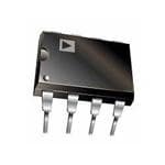
| 产品图片 |
|
| rohs | 符合RoHS无铅 / 符合限制有害物质指令(RoHS)规范要求 |
| 产品系列 | 放大器 IC,特殊用途放大器,Analog Devices SSM2141PZ- |
| 数据手册 | |
| 产品型号 | SSM2141PZ |
| 产品培训模块 | http://www.digikey.cn/PTM/IndividualPTM.page?site=cn&lang=zhs&ptm=30008http://www.digikey.cn/PTM/IndividualPTM.page?site=cn&lang=zhs&ptm=26202 |
| 产品目录页面 | |
| 产品种类 | 特殊用途放大器 |
| 供应商器件封装 | 8-PDIP |
| 共模抑制比—最小值 | 80 dB |
| 包装 | 管件 |
| 压摆率 | 9.5 V/µs |
| 商标 | Analog Devices |
| 增益带宽积 | - |
| 安装类型 | 通孔 |
| 安装风格 | Through Hole |
| 封装 | Tube |
| 封装/外壳 | 8-DIP(0.300",7.62mm) |
| 封装/箱体 | PDIP-8 |
| 工作温度 | -40°C ~ 85°C |
| 工作电源电压 | 18 V |
| 工厂包装数量 | 50 |
| 放大器类型 | 音频 |
| 最大双重电源电压 | +/- 18 V |
| 最大工作温度 | + 85 C |
| 最小工作温度 | - 40 C |
| 标准包装 | 50 |
| 电压-电源,单/双 (±) | ±6 V ~ 18 V |
| 电压-输入失调 | 25µV |
| 电流-电源 | 2.5mA |
| 电流-输入偏置 | - |
| 电流-输出/通道 | 45mA |
| 电源电压-最大 | 18 V |
| 电源电压-最小 | - 18 V |
| 电源电流 | 2.5 mA |
| 电路数 | 1 |
| 类型 | Differential Line Receiver |
| 系列 | SSM2141 |
| 视频文件 | http://www.digikey.cn/classic/video.aspx?PlayerID=1364138032001&width=640&height=505&videoID=2245193153001http://www.digikey.cn/classic/video.aspx?PlayerID=1364138032001&width=640&height=505&videoID=2245193159001 |
| 输入电压范围—最大 | 18 V |
| 输入补偿电压 | 25 uV |
| 输出类型 | - |
| 通道数量 | 1 Channel |


- 商务部:美国ITC正式对集成电路等产品启动337调查
- 曝三星4nm工艺存在良率问题 高通将骁龙8 Gen1或转产台积电
- 太阳诱电将投资9.5亿元在常州建新厂生产MLCC 预计2023年完工
- 英特尔发布欧洲新工厂建设计划 深化IDM 2.0 战略
- 台积电先进制程称霸业界 有大客户加持明年业绩稳了
- 达到5530亿美元!SIA预计今年全球半导体销售额将创下新高
- 英特尔拟将自动驾驶子公司Mobileye上市 估值或超500亿美元
- 三星加码芯片和SET,合并消费电子和移动部门,撤换高东真等 CEO
- 三星电子宣布重大人事变动 还合并消费电子和移动部门
- 海关总署:前11个月进口集成电路产品价值2.52万亿元 增长14.8%


PDF Datasheet 数据手册内容提取
a High Common-Mode Rejection Differential Line Receiver SSM2141 FEATURES FUNCTIONAL BLOCK DIAGRAM High Common-Mode Rejection DC: 100 dB typ 60 Hz: 100 dB typ 25kW 25kW –IN 2 5 SENSE 20 kHz: 70 dB typ 40 kHz: 62 dB typ 7 +VCC Low Distortion: 0.001% typ Fast Slew Rate: 9.5 V/(cid:109)s typ SSM2141 6 OUTPUT Wide Bandwidth: 3 MHz typ Low Cost Complements SSM2142 Differential Line Driver 4 –VEE 25kW 25kW APPLICATIONS +IN 3 1 REFERENCE Line Receivers Summing Amplifiers Buffer Amplifiers–Drives 600 (cid:86) Load PIN CONNECTIONS 8-Pin Plastic Mini-DIP (P Suffix) Narrow Body SO GENERAL DESCRIPTION (S Suffix) The SSM2141 is an integrated differential amplifier intended to receive balanced line inputs in audio applications requiring a high level of noise immunity and optimum common-mode REFERENCE 1 8 NC rejection. The SSM2141 typically achieves 100 dB of common- –IN 2 SSM2141 7 V+ mode rejection (CMR), whereas implementing an op amp with +IN 3 TOP VIEW 6 OUTPUT (Not to Scale) four off-the-shelf precision resistors will typically achieve only V– 4 5 SENSE 40 dB of CMR—inadequate for high-performance audio. NC = NO CONNECT The SSM2141 achieves low distortion performance by maintaining a large slew rate of 9.5 V/m s and high open-loop gain. Distortion is less than 0.002% over the full audio bandwidth. The SSM2141 complements the SSM2142 balanced line driver. Together, these devices comprise a fully integrated solution for equivalent transformer balancing of audio signals without the problems of distortion, EMI fields, and high cost. Additional applications for the SSM2141 include summing signals, differential preamplifiers, and 600 W low distortion buffer amplifiers. For similar performance with G = 1/2, see SSM2143. REV.C Information furnished by Analog Devices is believed to be accurate and reliable. However, no responsibility is assumed by Analog Devices for its use, nor for any infringements of patents or other rights of third parties which may result from its use. No license is granted by implication or One Technology Way, P.O. Box 9106, Norwood, MA 02062-9106, U.S.A. otherwise under any patent or patent rights of Analog Devices. Tel: 617/329-4700 Fax: 781/461-3113
SSM2141–SPECIFICATIONS ELECTRICAL CHARACTERISTICS (@ V = (cid:54)18 V, T = +25(cid:56)C, unless otherwise noted) S A SSM2141 Parameter Symbol Conditions Min Typ Max Units OFFSET VOLTAGE V V = 0 V –1000 25 1000 m V OS CM GAIN ERROR No Load, V = – 10 V, R = 0 W 0.001 0.01 % IN S INPUT VOLTAGE RANGE IVR (Note 1) – 10 V COMMON-MODE REJECTION CMR V = – 10 V 80 100 dB CM POWER SUPPLY REJECTION RATIO PSRR V = – 6 V to – 18 V 0.7 15 m V/V S OUTPUT SWING V R = 2 kW – 13 – 14.7 V O L SHORT-CIRCUIT CURRENT LIMIT I Output Shorted to Ground +45/–15 mA SC SMALL-SIGNAL BANDWIDTH (–3 dB) BW R = 2 kW 3 MHz L SLEW RATE SR R = 2 kW 6 9.5 V/m s L TOTAL HARMONIC DISTORTION R = 100 kW 0.001 % L THD R = 600 W 0.01 L CAPACITIVE LOAD DRIVE CAPABILITY C No Oscillation 300 pF L SUPPLY CURRENT I No Load 2.5 3.5 mA SY NOTES 1Input Voltage Range Guaranteed by CMR test. Specifications subject to change without notice ELECTRICAL CHARACTERISTICS (@ V = (cid:54)18 V, –40(cid:56)C £ T £ +85(cid:56)C) S A Parameter Symbol Conditions Min Typ Max Units OFFSET VOLTAGE V V = 0 V –2500 200 2500 m V OS CM GAIN ERROR No Load, V = – 10 V, R = 0 W 0.002 0.02 % IN S INPUT VOLTAGE RANGE IVR (Note 1) – 10 V COMMON-MODE REJECTION CMR V = – 10 V 75 90 dB CM POWER SUPPLY REJECTION RATIO PSRR V = – 6 V to – 18 V 1.0 20 m V/V S OUTPUT SWING V R = 2 kW – 13 – 14.7 V O L SLEW RATE SR R = 2 kW 9.5 V/m s L SUPPLY CURRENT I No Load 2.6 4.0 mA SY NOTES 1Input Voltage Range Guaranteed by CMR test. Specifications subject to change without notice –2– REV. C
SSM2141 ABSOLUTE MAXIMUM RATINGS1 Package Type (cid:117) 2 (cid:117) Units Supply Voltage . . . . . . . . . . . . . . . . . . . . . . . . . . . . . . . – 18 V JA JC Input Voltage1 . . . . . . . . . . . . . . . . . . . . . . . . Supply Voltage 8-Pin Plastic DIP (P) 103 43 (cid:176) C/W Output Short-Circuit Duration . . . . . . . . . . . . . . Continuous Storage Temperature Range NOTES 1For supply voltages less than – 18 V, the absolute maximum input voltage is equal P Package . . . . . . . . . . . . . . . . . . . . . . . –65(cid:176) C to +150(cid:176) C to the supply voltage. Lead Temperature (Soldering, 60 sec) . . . . . . . . . . . . +300(cid:176) C 2q is specified for worst case mounting conditions, i.e., q is specified for device JA JA Junction Temperature . . . . . . . . . . . . . . . . . . . . . . . . +150(cid:176) C in socket for P-DIP package. Operating Temperature Range . . . . . . . . . . . . –40(cid:176) C to +85(cid:176) C Typical Performance Characteristics Small Signal Transient Response Large Signal Transient Response Common-Mode Rejection vs. Frequency Power Supply Rejection vs. Frequency Total Harmonic Distortion vs. Frequency Dynamic Intermodulation Distortion vs. Frequency REV. C –3–
SSM2141–Typical Performance Characteristics Input Offset Voltage vs. Temperature Closed-Loop Gain vs. Frequency Closed-Loop Output Impedance vs. Frequency Gain Error vs. Temperature Slew Rate vs. Temperature Supply Current vs. Temperature Supply Current vs. Supply Voltage Maximum Output Voltage vs. Maximum Output Voltage vs. Output Current (Source) Output Current (Sink) –4– REV. C
SSM2141 5mV 1S +1µV 0V –1µV 0.1 TO 10Hz PEAK-TO-PEAK NOISE Voltage Noise Density vs. Frequency Low Frequency Voltage Noise 10mV 2mS 10mV 1mS +10µV +10µV 0V 0V –10µV –10µV TVAS == +–152V5(cid:176)C TVAS == +– 2155(cid:176)VC NOTE: EXTERNAL AMPLIFIER GAIN = 1000; NOTE: EXTERNAL AMPLIFIER GAIN = 1000; THEREFORE, VERTICAL SCALE = 10µV/DIV. THEREFORE, VERTICAL SCALE = 10µV/DIV. Voltage Noise from 0 kHz to 10 kHz Voltage Noise from 0 kHz to 1 kHz APPLICATIONS INFORMATION The SSM2141 represents a versatile analog building block. In order to capitalize on fast settling time, high slew rate, and high CMR, proper decoupling and grounding techniques must be employed. For decoupling, place 0.1 m F capacitor located within close proximity from each supply pin to ground. Slew Rate Test Circuit REV. C –5–
SSM2141 MAINTAINING COMMON-MODE REJECTION In order to achieve the full common-mode rejection capability of the SSM2141, the source impedance must be carefully controlled. Slight imbalances of the source resistance will result in a degradation of DC CMR—even a 5 W imbalance will degrade CMR by 20 dB. Also, the matching of the reactive source impedance must be matched in order to preserve the CMRR over frequency. Figure 5.Suitable Instrumentation Amplifier Requirements can be Addressed by Using an Input Stage Consisting of A, A, R and R 1 2 1 2 Figure 1.Precision Difference Amplifier. Rejects [E +E ] Common-Mode Signal = 1 2 by 100 dB 2 Figure 2.Precision Unity Gain Inverting Amplifier Figure 3.Precision Summing Amplifier Figure 4.Precision Summing Amplifier with Gain –6– REV. C
SSM2141 OUTLINE DIMENSIONS 0.400 (10.16) 0.365 (9.27) 0.355 (9.02) 8 5 0.280 (7.11) 0.250 (6.35) 1 4 0.240 (6.10) 0.325 (8.26) 0.310 (7.87) 0.100 (2.54) 0.300 (7.62) BSC 0.060 (1.52) 0.195 (4.95) 0.210 (5.33) MAX 0.130 (3.30) MAX 0.115 (2.92) 0.015 0.150 (3.81) (0.38) 0.015 (0.38) 0.130 (3.30) MIN GAUGE 0.115 (2.92) SEATING PLANE 0.014 (0.36) PLANE 0.010 (0.25) 0.022 (0.56) 0.008 (0.20) 0.005 (0.13) 0.430 (10.92) 0.018 (0.46) MIN MAX 0.014 (0.36) 0.070 (1.78) 0.060 (1.52) 0.045 (1.14) COMPLIANTTO JEDEC STANDARDS MS-001 CONTROLLING DIMENSIONSARE IN INCHES; MILLIMETER DIMENSIONS (RCINEOFRPEANRERERENN LCTEEHA EODSNSEL MSY)AAAYNR BDEE AR CROOEU NNNFODIGETUDAR-POEPFDRFOA INSPC RWHIAH ETOEQL UFEIO VORAR LU EHSNAETL ISFN FLDOEEARSDIGSN.. 070606-A Figure 6. 8-Lead Plastic Dual In-Line Package [PDIP] Narrow Body (N-8) Dimensions shown in inches and (millimeters) 5.00(0.1968) 4.80(0.1890) 8 5 4.00(0.1574) 6.20(0.2441) 3.80(0.1497) 1 4 5.80(0.2284) 1.27(0.0500) 0.50(0.0196) BSC 1.75(0.0688) 0.25(0.0099) 45° 0.25(0.0098) 1.35(0.0532) 8° 0.10(0.0040) 0° COPLANARITY 0.51(0.0201) 0.10 SEATING 0.31(0.0122) 0.25(0.0098) 10..2470((00..00510507)) PLANE 0.17(0.0067) COMPLIANTTOJEDECSTANDARDSMS-012-AA C(RINOEFNPEATRRREOENNLCLTEIHNEOGSNDELISYM)AEANNRDSEIAORRNOESUNANORDETEDAIN-POMPFRIFLOLMPIMIRLELIATIMTEEERTFSEO;RIRNECUQHSUEDIVIINMAELDENENSSTIIOGSNNFS.OR 012407-A Figure 7.8-Lead Standard Small Outline Package [SOIC_N] Narrow Body (R-8) Dimensions shown in millimeters and (inches) REV. C –7–
SSM2141 ORDERING GUIDE Model1 Temperature Range Package Description Package Option SSM2141PZ −40°C ≤ T ≤ +85°C 8-Lead PDIP N-8 A SSM2141SZ −40°C ≤ T ≤ +85°C 8-Lead SOIC_N R-8 A SSM2141SZ-REEL −40°C ≤ T ≤ +85°C 8-Lead SOIC_N R-8 A 1 Z = RoHS Compliant Part. REVISION HISTORY 6/11—Rev. B to Rev. C Updated Outline Dimensions ......................................................... 7 Changes to Ordering Guide ............................................................ 8 5/91—Rev. A to Rev. B ©2007 Analog Devices, Inc. All rights reserved. Trademarks and registered trademarks are the property of their respective owners. D10008-0-6/11(C) –8– REV. C
Mouser Electronics Authorized Distributor Click to View Pricing, Inventory, Delivery & Lifecycle Information: A nalog Devices Inc.: SSM2141SZ-REEL SSM2141PZ SSM2141SZ