ICGOO在线商城 > 集成电路(IC) > 线性 - 放大器 - 仪表,运算放大器,缓冲器放大器 > MC34071ADG
 Datasheet下载
- 型号: MC34071ADG
- 制造商: ON Semiconductor
- 库位|库存: xxxx|xxxx
- 要求:
| 数量阶梯 | 香港交货 | 国内含税 |
| +xxxx | $xxxx | ¥xxxx |
查看当月历史价格
查看今年历史价格
MC34071ADG产品简介:
ICGOO电子元器件商城为您提供MC34071ADG由ON Semiconductor设计生产,在icgoo商城现货销售,并且可以通过原厂、代理商等渠道进行代购。 MC34071ADG价格参考¥3.00-¥4.74。ON SemiconductorMC34071ADG封装/规格:线性 - 放大器 - 仪表,运算放大器,缓冲器放大器, 通用 放大器 1 电路 8-SOIC。您可以下载MC34071ADG参考资料、Datasheet数据手册功能说明书,资料中有MC34071ADG 详细功能的应用电路图电压和使用方法及教程。
MC34071ADG 是安森美半导体(ON Semiconductor)生产的一款高性能运算放大器,属于线性放大器类别中的运算放大器子类。该器件具有高增益、宽频带和良好的输入阻抗特性,适用于多种模拟信号处理场景。

应用场景包括:

1. 工业自动化与控制系统:用于传感器信号的放大与调理,如温度、压力、电流等微弱信号的检测和处理。

2. 电源管理电路:在开关电源或DC-DC转换器中作为误差放大器,用于反馈环路控制,提高电源稳定性与响应速度。

3. 测试与测量设备:在示波器、万用表、信号发生器等仪器中用于高精度信号放大与处理。

4. 音频处理电路:虽然不是专用音频运放,但在低噪声前置放大、音效处理电路中也有应用。

5. 汽车电子系统:如车载传感器接口、电池管理系统(BMS)中的信号调节模块。

6. 医疗设备:用于生物电信号(如心电、脑电)的前级放大,需配合其他元件实现高共模抑制比(CMRR)设计。

MC34071ADG 采用单电源供电,适合多种应用场景,具备较强的通用性和可靠性,广泛应用于需要高性能模拟信号处理的工业与消费电子领域。
| 参数 | 数值 |
| -3db带宽 | - |
| 产品目录 | 集成电路 (IC)半导体 |
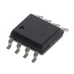
| 描述 | IC OPAMP GP 4.5MHZ 8SOIC运算放大器 - 运放 3-44V Single 3mV VIO Commercial Temp |
| 产品分类 | Linear - Amplifiers - Instrumentation, OP Amps, Buffer Amps集成电路 - IC |
| 品牌 | ON Semiconductor |
| 产品手册 | |
| 产品图片 |
|
| rohs | 符合RoHS无铅 / 符合限制有害物质指令(RoHS)规范要求 |
| 产品系列 | 放大器 IC,运算放大器 - 运放,ON Semiconductor MC34071ADG- |
| 数据手册 | |
| 产品型号 | MC34071ADG |
| 产品目录页面 | |
| 产品种类 | 运算放大器 - 运放 |
| 供应商器件封装 | 8-SOIC N |
| 共模抑制比—最小值 | 80 dB |
| 关闭 | No Shutdown |
| 其它名称 | MC34071ADG-ND |
| 包装 | 管件 |
| 压摆率 | 13 V/µs |
| 双重电源电压 | +/- 3 V, +/- 5 V, +/- 9 V |
| 商标 | ON Semiconductor |
| 增益带宽生成 | 4.5 MHz |
| 增益带宽积 | 4.5MHz |
| 安装类型 | 表面贴装 |
| 安装风格 | SMD/SMT |
| 封装 | Tube |
| 封装/外壳 | 8-SOIC(0.154",3.90mm 宽) |
| 封装/箱体 | SOIC-8 |
| 工作温度 | 0°C ~ 70°C |
| 工作电源电压 | 3 V to 44 V, +/- 1.5 V to +/- 22 V |
| 工厂包装数量 | 98 |
| 技术 | Bipolar |
| 放大器类型 | 通用 |
| 最大双重电源电压 | +/- 22 V |
| 最大工作温度 | + 70 C |
| 最小双重电源电压 | +/- 1.5 V |
| 最小工作温度 | 0 C |
| 标准包装 | 98 |
| 电压-电源,单/双 (±) | 3 V ~ 44 V, ±1.5 V ~ 22 V |
| 电压-输入失调 | 500µV |
| 电流-电源 | 1.9mA |
| 电流-输入偏置 | 100nA |
| 电流-输出/通道 | 30mA |
| 电源电流 | 1.9 mA |
| 电路数 | 1 |
| 系列 | MC34071A |
| 转换速度 | 13 V/us |
| 输入偏压电流—最大 | 500 nA |
| 输入参考电压噪声 | 32 nV |
| 输入补偿电压 | 3 mV |
| 输出电流 | 30 mA |
| 输出类型 | - |
| 通道数量 | 1 Channel |


- 商务部:美国ITC正式对集成电路等产品启动337调查
- 曝三星4nm工艺存在良率问题 高通将骁龙8 Gen1或转产台积电
- 太阳诱电将投资9.5亿元在常州建新厂生产MLCC 预计2023年完工
- 英特尔发布欧洲新工厂建设计划 深化IDM 2.0 战略
- 台积电先进制程称霸业界 有大客户加持明年业绩稳了
- 达到5530亿美元!SIA预计今年全球半导体销售额将创下新高
- 英特尔拟将自动驾驶子公司Mobileye上市 估值或超500亿美元
- 三星加码芯片和SET,合并消费电子和移动部门,撤换高东真等 CEO
- 三星电子宣布重大人事变动 还合并消费电子和移动部门
- 海关总署:前11个月进口集成电路产品价值2.52万亿元 增长14.8%


PDF Datasheet 数据手册内容提取
MC34071,2,4,A MC33071,2,4,A, NCV33072,4,A Single Supply 3.0 V to 44 V Operational Amplifiers Quality bipolar fabrication with innovative design concepts are hhttttpp::////oonnsseemmii..ccoomm employed for the MC33071/72/74, MC34071/72/74, NCV33072/74A series of monolithic operational amplifiers. This series of operational amplifiers offer 4.5 MHz of gain bandwidth product, 13 V/(cid:2)s slew rate PDIP−8 P SUFFIX and fast settling time without the use of JFET device technology. 8 CASE 626 Although this series can be operated from split supplies, it is 1 particularly suited for single supply operation, since the common mode input voltage range includes ground potential (V ). With a EE Darlington input stage, this series exhibits high input resistance, low SOIC−8 8 D SUFFIX input offset voltage and high gain. The all NPN output stage, CASE 751 characterized by no deadband crossover distortion and large output 1 voltage swing, provides high capacitance drive capability, excellent phase and gain margins, low open loop high frequency output impedance and symmetrical source/sink AC frequency response. WQFN10 MT SUFFIX The MC33071/72/74, MC34071/72/74, NCV33072/74,A series of CASE 510AJ devices are available in standard or prime performance (A Suffix) grades and are specified over the commercial, industrial/vehicular or military temperature ranges. The complete series of single, dual and quad operational amplifiers are available in plastic DIP, SOIC, QFN and TSSOP surface mount packages. PDIP−14 Features P SUFFIX • CASE 646 Wide Bandwidth: 4.5 MHz 14 • High Slew Rate: 13 V/(cid:2)s 1 • Fast Settling Time: 1.1 (cid:2)s to 0.1% SOIC−14 • Wide Single Supply Operation: 3.0 V to 44 V 14 D SUFFIX • CASE 751A Wide Input Common Mode Voltage Range: Includes Ground (VEE) 1 • Low Input Offset Voltage: 3.0 mV Maximum (A Suffix) • Large Output Voltage Swing: −14.7 V to +14 V (with ±15 V TSSOP−14 Supplies) DTB SUFFIX • 14 Large Capacitance Drive Capability: 0 pF to 10,000 pF CASE 948G 1 • Low Total Harmonic Distortion: 0.02% • Excellent Phase Margin: 60° ORDERING INFORMATION • Excellent Gain Margin: 12 dB See detailed ordering and shipping information on page 18 of • Output Short Circuit Protection this data sheet. • ESD Diodes/Clamps Provide Input Protection for Dual and Quad DEVICE MARKING INFORMATION • NCV Prefix for Automotive and Other Applications Requiring See general marking information in the device marking Unique Site and Control Change Requirements; AEC−Q100 section on page 21 of this data sheet. Qualified and PPAP Capable • These Devices are Pb−Free, Halogen Free/BFR Free and are RoHS Compliant © Semiconductor Components Industries, LLC, 2014 1 Publication Order Number: July, 2014 − Rev. 22 MC34071/D
MC34071,2,4,A MC33071,2,4,A, NCV33072,4,A PIN CONNECTIONS CASE 626/CASE 751 CASE 646/CASE 751A/CASE 948G CASE 510AJ VCC Offset Null 1 8 NC Output 1 1 14 Output 4 10 Inputs 23 -+ 76 VOCuCtput Inputs 1 2 -+ 1 4 -+ 13 Inputs 4 Output 1 1 9 Output 2 3 12 VEE 4 5 Offset Null NC 2 8 NC VCC 4 11 VEE (Single, Top View) In 1 3 7 In 2 Inputs 2 5 +- 2 3 +- 10 Inputs 3 In + 1 4 6 In + 2 Output 1 1 8 VCC 6 9 5 2 - 7 Output 2 Output 2 7 8 Output 3 Inputs 1 3 + 6 VEE/GND - Inputs 2 VEE 4 + 5 (Quad, Top View) (Top View) (Dual, Top View) VCC Q3 Q4 Q5 Q6 Q7 Q1 Q17 Q2 R1 C1 R2 D2 Q18 Bias - Q8 Q9 Q10 Q11 R6 R7 Output Inputs R8 + C2 D3 Q19 Base Q13 Q14 Q15 Q16 Current Cancellation Q12 Current D1 Limit R5 R3 R4 VEE/GND Offset Null (MC33071, MC34071 only) Figure 1. Representative Schematic Diagram (Each Amplifier) http://onsemi.com 2
MC34071,2,4,A MC33071,2,4,A, NCV33072,4,A MAXIMUM RATINGS Rating Symbol Value Unit Supply Voltage (from VEE to VCC) VS +44 V Input Differential Voltage Range VIDR (Note 1) V Input Voltage Range VIR (Note 1) V Output Short Circuit Duration (Note 2) tSC Indefinite Sec Operating Junction Temperature TJ +150 °C Storage Temperature Range Tstg −60 to +150 °C ESD Capability, Dual and Quad (Note 3) V Human Body Model ESDHBM 2000 Machine Model ESDMM 200 Stresses exceeding those listed in the Maximum Ratings table may damage the device. If any of these limits are exceeded, device functionality should not be assumed, damage may occur and reliability may be affected. 1. Either or both input voltages should not exceed the magnitude of VCC or VEE. 2. Power dissipation must be considered to ensure maximum junction temperature (TJ) is not exceeded (see Figure 2). 3. This device series incorporates ESD protection and is tested by the following methods: ESD Human Body Model tested per AEC−Q100−002 (JEDEC standard: JESD22−A114) ESD Machine Model tested per AEC−Q100−003 (JEDEC standard: JESD22−A115) http://onsemi.com 3
MC34071,2,4,A MC33071,2,4,A, NCV33072,4,A ELECTRICAL CHARACTERISTICS (VCC = +15 V, VEE = −15 V, RL = connected to ground, unless otherwise noted. See Note 4 for TA = Tlow to Thigh) A Suffix Non−Suffix Characteristics Symbol Min Typ Max Min Typ Max Unit InpVuCt CO =ff s+e1t5 V Vo,lt aVgEeE (=R −S1 =5 1V0, 0T A(cid:3) =, V +C2M5 °=C 0 V, VO = 0 V) VIO −− 0.5 3.0 −− 1.0 5.0 mV VCC = +5.0 V, VEE = 0 V, TA = +25°C − 0.5 3.0 − 1.5 5.0 VCC = +15 V, VEE = −15 V, TA = Tlow to Thigh − 5.0 − 7.0 Average Temperature Coefficient of Input Offset (cid:4)VIO/(cid:4)T − 10 − − 10 − (cid:2)V/°C Voltage RS = 10 (cid:3), VCM = 0 V, VO = 0 V, TA = Tlow to Thigh Input Bias Current (VCM = 0 V, VO = 0 V) IIB nA TA = +25°C − 100 500 − 100 500 TA = Tlow to Thigh − − 700 − − 700 Input Offset Current (VCM = 0 V, VO = 0V) IIO nA TA = +25°C − 6.0 50 − 6.0 75 TA = Tlow to Thigh − − 300 − − 300 Input Common Mode Voltage Range VICR V TA = +25°C VEE to (VCC −1.8) VEE to (VCC −1.8) TA = Tlow to Thigh VEE to (VCC −2.2) VEE to (VCC −2.2) Large Signal Voltage Gain (VO = ±10 V, RL = 2.0 k(cid:3)) AVOL V/mV TA = +25°C 50 100 − 25 100 − TA = Tlow to Thigh 25 − − 20 − − Output Voltage Swing (VID = ±1.0 V) VOH V VCC = +5.0 V, VEE = 0 V, RL = 2.0 k(cid:3), TA = +25°C 3.7 4.0 − 3.7 4.0 − VCC = +15 V, VEE = −15 V, RL = 10 k(cid:3), TA = +25°C 13.6 14 − 13.6 14 − VCC = +15 V, VEE = −15 V, RL = 2.0 k(cid:3), 13.4 − − 13.4 − − TA = Tlow to Thigh VCC = +5.0 V, VEE = 0 V, RL = 2.0 k(cid:3), TA = +25°C VOL − 0.1 0.3 − 0.1 0.3 V VCC = +15 V, VEE = −15 V, RL = 10 k(cid:3), TA = +25°C − −14.7 −14.3 − −14.7 −14.3 VCC = +15 V, VEE = −15 V, RL = 2.0 k(cid:3), − − −13.5 − − −13.5 TA = Tlow to Thigh Output Short Circuit Current (VID = 1.0 V, VO = 0 V, ISC mA TA = 25°C) Source 10 30 − 10 30 − Sink 20 30 − 20 30 − Common Mode Rejection CMR 80 97 − 70 97 − dB RS ≤ 10 k(cid:3), VCM = VICR, TA = 25°C Power Supply Rejection (RS = 100 (cid:3)) PSR 80 97 − 70 97 − dB VCC/VEE = +16.5 V/−16.5 V to +13.5 V/−13.5 V, TA = 25°C Power Supply Current (Per Amplifier, No Load) ID mA VCC = +5.0 V, VEE = 0 V, VO = +2.5 V, TA = +25°C − 1.6 2.0 − 1.6 2.0 VCC = +15 V, VEE = −15 V, VO = 0 V, TA = +25°C − 1.9 2.5 − 1.9 2.5 VCC = +15 V, VEE = −15 V, VO = 0 V, − − 2.8 − − 2.8 TA = Tlow to Thigh Product parametric performance is indicated in the Electrical Characteristics for the listed test conditions, unless otherwise noted. Product performance may not be indicated by the Electrical Characteristics if operated under different conditions. 4. Tlow = −40°C for MC33071,2,4,/A, NCV33074/AThigh = +85°C for MC33071,2,4,/A, NCV33074/A = 0°C for MC34071,2,4,/A = +70°C for MC34071,2,4,/A = −40°C for MC34072,4/V, NCV33072,4A = +125°C for MC34072,4/V, NCV33072,4A, NCV34074V Case 510AJ Tlow/Thigh guaranteed by product characterization. http://onsemi.com 4
MC34071,2,4,A MC33071,2,4,A, NCV33072,4,A AC ELECTRICAL CHARACTERISTICS (VCC = +15 V, VEE = −15 V, RL = connected to ground. TA = +25°C, unless otherwise noted.) A Suffix Non−Suffix Characteristics Symbol Min Typ Max Min Typ Max Unit Slew Rate (Vin = −10 V to +10 V, RL = 2.0 k(cid:3), CL = 500 pF) SR V/(cid:2)s AV = +1.0 8.0 10 − 8.0 10 − AV = −1.0 − 13 − − 13 − Setting Time (10 V Step, AV = −1.0) ts (cid:2)s To 0.1% (+1/2 LSB of 9−Bits) − 1.1 − − 1.1 − To 0.01% (+1/2 LSB of 12−Bits) − 2.2 − − 2.2 − Gain Bandwidth Product (f = 100 kHz) GBW 3.5 4.5 − 3.5 4.5 − MHz Power Bandwidth BW − 160 − − 160 − kHz AV = +1.0, RL = 2.0 k(cid:3), VO = 20 Vpp, THD = 5.0% Phase margin fm Deg RL = 2.0 k(cid:3) − 60 − − 60 − RL = 2.0 k(cid:3), CL = 300 pF − 40 − − 40 − Gain Margin Am dB RL = 2.0 k(cid:3) − 12 − − 12 − RL = 2.0 k(cid:3), CL = 300 pF − 4.0 − − 4.0 − Equivalent Input Noise Voltage en − 32 − − 32 − nV/√Hz RS = 100 (cid:3), f = 1.0 kHz Equivalent Input Noise Current in − 0.22 − − 0.22 − pA/√Hz f = 1.0 kHz Differential Input Resistance Rin − 150 − − 150 − M(cid:3) VCM = 0 V Differential Input Capacitance Cin − 2.5 − − 2.5 − pF VCM = 0 V Total Harmonic Distortion THD − 0.02 − − 0.02 − % AV = +10, RL = 2.0 k(cid:3), 2.0 Vpp ≤ VO ≤ 20 Vpp, f = 10 kHz Channel Separation (f = 10 kHz) − − 120 − − 120 − dB Open Loop Output Impedance (f = 1.0 MHz) |ZO| − 30 − − 30 − W Single Supply Split Supplies 3.0 V to 44 V VCC+|VEE|≤44 V VCC VCC VCC 7 2 - 1 VCC 1 6 3 + 5 2 2 1 4 3 3 10 k 4 VEE 4 VEE VEE VEE Offset nulling range is approximately ±80 mV with a 10 k potentiometer (MC33071, MC34071 only). Figure 2. Power Supply Configurations Figure 3. Offset Null Circuit http://onsemi.com 5
MC34071,2,4,A MC33071,2,4,A, NCV33072,4,A 2400 W) TION (m 2000 GE (mV) 4.0 VVVCECECM === -+01155 VV SSIPA 1600 OLTA 2.0 ER DI 1200 SOIC-14 Pkg 8 & 14 Pin Plastic Pkg SET V 0 W F M PO 800 UT OF-2.0 U P M SOIC-8 Pkg N AXI 400 (cid:4)(cid:3), IO P(cid:3)(cid:3)(cid:3), MD 0 VVI-4.0 -55 -40 -20 0 20 40 60 80 100 120 140 160 -55 -25 0 25 50 75 100 125 TA, AMBIENT TEMPERATURE (°C) TA, AMBIENT TEMPERATURE (°C) Figure 4. Maximum Power Dissipation versus Figure 5. Input Offset Voltage versus Temperature for Package Types Temperature for Representative Units V) VCC NGE (D) 1.3 VCC -0.8 VCC VCC/VEE = +1.5 V/ -1.5 V to +22 V/ -22 V TAGE RARMALIZE 1.2 VVVCECECM === - 0+1155 V V LO ON 1.1 VCC -1.6 MODE VRRENT ( 1.0 N U VCC -2.4 MOS C 0.9 MA OBI VEE +0.01 UT CPUT 0.8 VEE-55 -25 0 VEE 25 50 75 100 125(cid:4)(cid:3)(cid:3)(cid:3), INPCRI(cid:4), INIB0.7-55 -25 0 25 50 75 100 125 VI TA, AMBIENT TEMPERATURE (°C) TA, AMBIENT TEMPERATURE (°C) Figure 6. Input Common Mode Voltage Figure 7. Normalized Input Bias Current Range versus Temperature versus Temperature D) 1.4 50 E ORMALIZ 1.2 TVVACE EC= ==2 5- +°1C155 V V G (V)pp 40 RtoL G Croonunnedc TteAd = 25°C N N T ( WI N S 30 URRE 1.0 TAGE RL = 10 k RL = 2.0 k C L T BIAS 0.8 PUT VO 20 PU UT 10 N O (cid:4), IB , O I V I 0.6 0 -12 -8.0 -4.0 0 4.0 8.0 12 0 5.0 10 15 20 25 VIC, INPUT COMMON MODE VOLTAGE (V) VCC, |VEE|, SUPPLY VOLTAGE (V) Figure 8. Normalized Input Bias Current versus Figure 9. Split Supply Output Voltage Input Common Mode Voltage Swing versus Supply Voltage http://onsemi.com 6
MC34071,2,4,A MC33071,2,4,A, NCV33072,4,A E (V) VCC Source VCC/VEE = +4.5 V/ -4.5 V to +22 V/ -22 V E (V) VCC VCC G G OLTA VCC -1.0 −40 OLTAVCC-2.0 VCC = +15 V N V 25 N V RL = GND TIO VCC -2.0 125 TIOVCC-4.0 TA = 25°C A A R R U U SAT VEE +2.0 Sink SAT 0.2 T T U U P 25 P UT VEE +1.0 UT 0.1 O 85 O V , sat VEE 125 V , sat 0 GND 0 5.0 10 15 20 100 1.0 k 10 k 100 k IL, LOAD CURRENT (±mA) RL, LOAD RESISTANCE TO GROUND ((cid:3)) Figure 10. Split Supply Output Saturation Figure 11. Single Supply Output Saturation versus Load Current versus Load Resistance to Ground V) 0 60 E ( LTAG-0.4 VCC mA) 50 Sink N VO NT ( 40 TURATIO-0.8 T CURRE 30 Source V , OUTPUT SAsat 21..00 GND VRTACL C=to =2 V 5+C°1CC5 V I(cid:5)(cid:5)(cid:3)(cid:3), OUTPUSC21000 VRV(cid:4)CELV EC≤in = = 0= -.+ 1111 .5(cid:3)05 VVV 100 1.0 k 10 k 100 k -55 -25 0 25 50 75 100 125 RL, LOAD RESISTANCE TO VCC ((cid:3)) TA, AMBIENT TEMPERATURE (°C) Figure 12. Single Supply Output Saturation Figure 13. Output Short Circuit Current versus Load Resistance to V versus Temperature CC 50 28 VCC = +15 V ΩPEDANCE ((cid:4)) 4300 VV(cid:4)TVAECOI OEM == == =20 5 -±0°10C5.5 V mA GE SWING (V)pp 221406 VARTTVAVHCEL ECD=== = =2+2≤ 5.1-+ 01°.11 0.Ck505 % VV T IM 20 OLTA 12 OUTPU AV = 1000 AV = 100 AV = 10 AV = 1.0 PUT V 8.0 Z(cid:5)(cid:3), O 10 OUT 4.0 , O V 0 0 1.0 k 10 k 100 1.0 M 10 M 3.0 k 10 k 30 k 100 k 300 k 1.0 M 3.0 M f, FREQUENCY (Hz) f, FREQUENCY (Hz) Figure 14. Output Impedance Figure 15. Output Voltage Swing versus Frequency versus Frequency http://onsemi.com 7
MC34071,2,4,A MC33071,2,4,A, NCV33072,4,A 0.4 4.0 %) %) TORTION ( 0.3 AV = 1000 TORTION ( 3.0 AV = 1000 VVRTACEL EC== ==22 5.- 0+°1 C1k55 V V C DIS VVCEEC == - +1155 V V C DIS NI 0.2 VO = 2.0 Vpp NI 2.0 MO RL = 2.0 k MO HAR AV = 100 TA = 25°C HAR AV = 100 TAL 0.1 TAL 1.0 AV = 10 D, TO AV = 10 D, TO AV = 1.0 TH 0 AV = 1.0 TH 0 10 100 1.0 k 10 k 100 k 0 4.0 8.0 12 16 20 f, FREQUENCY (Hz) VO, OUTPUT VOLTAGE SWING (Vpp) Figure 16. Total Harmonic Distortion Figure 17. Total Harmonic Distortion versus Frequency versus Output Voltage Swing 116 100 B) B) d d 0 AIN (112 VCC = +15 V AIN ( 80 S) GE G VVEOE= =- 1-01 5V Vto +10 V GE G Phase Gain 45 GREE P VOLTA108 Rf ≤L =1 01H0z k P VOLTA 60 MPhaargsien 90 ASE (DE OO104 OO 40 = 60° PH N L N L VCC = +15 V 135SS PE PE VEE = -15 V CE A(cid:4)(cid:3)(cid:3)(cid:3), OVOL100 A(cid:4)(cid:3)(cid:3)(cid:3), OVOL20 VRTAOL === 2205. 0V° Ck 180φ, EX 96 0 -55 -25 0 25 50 75 100 125 1.0 10 100 1.0 k 10 k 100 k 1.0 M 10 M 100 M TA, AMBIENT TEMPERATURE (°C) f, FREQUENCY (Hz) Figure 18. Open Loop Voltage Gain Figure 19. Open Loop Voltage Gain and versus Temperature Phase versus Frequency D) E B) 20 1 ALI 1.15 AIN (d 10 PMhaargsien = 60° 100 NORM 1.1 VVCEEC == - +1155 V V LTAGE G 0 GMaairngin = 12 dB 112400EGREES) ODUCT ( 1.05 RL = 2.0 k O D R P V-10 E ( H P 1.0 A(cid:4)(cid:3)(cid:3)(cid:3), OPEN LOOVOL---234000 1234VVV....CEO PPGGEC = hh aa== aa0ii nn ss1+ Vee5RR1 (cid:4) 5LLRRV LL==V(cid:4) ==22 ..(cid:4)2200.. 00kk(cid:4) ,kk C,(cid:4) LC L=T A=3 0=30 02 0p5 F°pCF 2 43 116800φ, EXCESS PHAS W, GAIN BANDWIDT 00..098.559 B 1.0 2.0 3.0 5.0 7.0 10 20 30 G -55 -25 0 25 50 75 100 125 f, FREQUENCY (MHz) TA, AMBIENT TEMPERATURE (°C) Figure 20. Open Loop Voltage Gain and Figure 21. Normalized Gain Bandwidth Phase versus Frequency Product versus Temperature http://onsemi.com 8
MC34071,2,4,A MC33071,2,4,A, NCV33072,4,A 100 70 VCC = +15 V S) 60 VCC = +15 V 80 VEE = -15 V EE VEE = -15 V T OVERSHOOT 60 RVTAOL === 22-5.10°0 Ck V to +10 V MARGIN (DEGR 543000 ARVTAVOL ==== 2+2-5.110°.0 0Ck V to t o(cid:2) +10 V PERCEN 4200 , PHASE m20 φ 10 0 0 10 100 1.0 k 10 k 10 100 1.0 k 10 k CL, LOAD CAPACITANCE (pF) CL, LOAD CAPACITANCE (pF) Figure 22. Percent Overshoot versus Figure 23. Phase Margin versus Load Capacitance Load Capacitance 14 80 12 VVCEEC == - +1155 V V EES) CL = 10 pF N (dB) 10 ARVL == +2.10. 0k to ∞ DEGR 60 CL = 100 pF ARGI 8.0 VTAO == 2-51°0C V to +10 V GIN ( VCC = +15 V A(cid:4), GAIN Mm64..00 PHASE MAR 2400 CL = 1,000 pF VARVVEOL E === = +2- .1-10.10 0k5 V tVo t o∞ +10 V , m 2.0 φ CL = 10,000 pF 0 0 10 100 1.0 k 10 k -55 -25 0 25 50 75 100 125 CL, LOAD CAPACITANCE (pF) TA, AMBIENT TEMPERATURE (°C) Figure 24. Gain Margin versus Load Capacitance Figure 25. Phase Margin versus Temperature 16 12 70 VCC = +15 V 10 60 S) A(cid:4), GAIN MARGIN (dB)m841..200 VARVVEOL E === = +2C- .1 10L-.0 01=k 5V 1t o V,t0 o∞0 +01 p0F V CLC =L =1C 01L0 0= ,p 01F000 p pFF A(cid:4), GAIN MARGIN (dB)m8642....0000 VVRAVCET EC== RR = =+R2 1 1- 1+01 +105- 5+ RV V2 VO GainPhase 54320000 , PHASE MARGIN (DEGREEm 0 VO = 0 V 10φ TA = 25°C 0 0 -55 -25 0 25 50 75 100 125 1.0 10 100 1.0 k 10 k 100 k TA, AMBIENT TEMPERATURE (°C) RT, DIFFERENTIAL SOURCE RESISTANCE ((cid:3)) Figure 26. Gain Margin versus Temperature Figure 27. Phase Margin and Gain Margin versus Differential Source Resistance http://onsemi.com 9
MC34071,2,4,A MC33071,2,4,A, NCV33072,4,A 1.15 V) 10 LIZED) 1.1 VVAVCE EC= ==+ 1- +.10155 V V ROM 0 V ( 5.0 10 mV 1.0 mV 1.0 mV VVAVCE EC= ==- 1- +.10155 V V MA1.05 RL = 2.0 k G F TA = 25°C W RATE (NOR0.19.50 CL = 500 pF OLTAGE SWIN 0 UCnocmopmepnesnasteadted SLE T V-5.0 1.0 mV R, 0.9 PU 10 mV S UT 1.0 mV O 0.85 (cid:4), O-10 -55 -25 0 25 50 75 100 125 V 0 0.5 1.0 1.5 2.0 2.5 3.0 3.5 Δ TA, AMBIENT TEMPERATURE (°C) ts, SETTLING TIME ((cid:2)s) Figure 28. Normalized Slew Rate Figure 29. Output Settling Time versus Temperature VCC = +15 V VEE = -15 V AV = +1.0 RL = 2.0 k 50 mV/DIV 0 VVCEEC == -+1155 VV 5.0 V/DIV 0 CTAL == 2350°0C pF AV = +1.0 RL = 2.0 k CL = 300 pF TA = 25°C 2.0 (cid:2)s/DIV 1.0 (cid:2)s/DIV Figure 30. Small Signal Transient Response Figure 31. Large Signal Transient Response 100 100 dB) TA = 125°C VCC = +15 V B) VCC = +15 V TION ( 80 TA = 25°C VVECEM == -01 V5 V ON (d 80 VTAE E= =2 5-°1C5 V EC TA = -55°C (cid:4)VCM = ±1.5 V CTI (cid:4)VCC E REJ 60 REJE 60 -ADM (cid:4)VO ((cid:4)VCC = +1.5 V) D Y + O L OMMON M 40 (cid:4)VCM -A+DM (cid:4)VO WER SUPP 40 +PSR = 20 L(cid:4)ogVEE (cid:4)V(cid:4)OV/CACDM +PSR CMR, C 200 CMR = 20 Log (cid:4)(cid:4)VVCOM x ADM PSR, PO 200 -PSR = 20 Log (cid:4)V(cid:4)OV/EAEDM ((cid:4)VEE = -+P1S.5R V) 0.1 1.0 10 100 1.0 k 10 k 100 k 1.0 M 10 M 0.1 1.0 10 100 1.0 k 10 k 100 k 1.0 M 10 M f, FREQUENCY (Hz) f, FREQUENCY (Hz) Figure 32. Common Mode Rejection Figure 33. Power Supply Rejection versus Frequency versus Frequency http://onsemi.com 10
MC34071,2,4,A MC33071,2,4,A, NCV33072,4,A 9.0 105 mA) 8.0 TA = -55°C ON (dB) -PSR ((cid:4)VEE = +1.5 V) VVCEEC == - +1155 V V T ( CTI95 N E URRE 7.0 TA = 25°C Y REJ +PSR ((cid:4)VCC = +1.5 V) I(cid:4)(cid:3) , SUPPLY CCC65..00 TA = 125°C Quad device PSR, POWER SUPPL8755 +-PPSSRR == 2200 LLoogg (cid:4)(cid:4)(cid:4)(cid:4)VVOOVV//CEAAECDDMM -A+DM (cid:4)(cid:4)VVCEEC (cid:4)VO 4.0 65 0 5.0 10 15 20 25 -55 -25 0 25 50 75 100 125 VCC, |VEE|, SUPPLY VOLTAGE (V) TA, AMBIENT TEMPERATURE (°C) Figure 34. Supply Current versus Figure 35. Power Supply Rejection Supply Voltage versus Temperature 120 70 2.8 CHANNEL SEPARATION (dB)18642000000 VVTACE EC= ==2 5- +°1C155 V V √NPUT NOICE VOLTAGE (nVHz(cid:3)) 6543200000 CuVrroeltnatge VVVTACEC ECM= ===2 5 - 0+°1C155 V V 22110.....40628 √PUT NOISE CURRENT (pA )Hz e(cid:5)(cid:3)(cid:3), In 10 0.4 (cid:4), INn 0 0 0 i 10 20 30 50 70 100 200 300 10 100 1.0 k 10 k 100 k f, FREQUENCY (kHz) f, FREQUENCY (kHz) Figure 36. Channel Separation versus Frequency Figure 37. Input Noise versus Frequency APPLICATIONS INFORMATION CIRCUIT DESCRIPTION/PERFORMANCE FEATURES Although the bandwidth, slew rate, and settling time of the up to approximately 5.0 mA of current from V through EE MC34071 amplifier series are similar to op amp products either inputs clamping diode without damage or latching, utilizing JFET input devices, these amplifiers offer other although phase reversal may again occur. additional distinct advantages as a result of the PNP If one or both inputs exceed the upper common mode transistor differential input stage and an all NPN transistor voltage limit, the amplifier output is readily predictable and output stage. may be in a low or high state depending on the existing input Since the input common mode voltage range of this input bias conditions. stage includes the V potential, single supply operation is Since the input capacitance associated with the small EE feasible to as low as 3.0 V with the common mode input geometry input device is substantially lower (2.5 pF) than voltage at ground potential. the typical JFET input gate capacitance (5.0 pF), better The input stage also allows differential input voltages up frequency response for a given input source resistance can to ±44 V, provided the maximum input voltage range is not be achieved using the MC34071 series of amplifiers. This exceeded. Specifically, the input voltages must range performance feature becomes evident, for example, in fast between V and V supply voltages as shown by the settling D−to−A current to voltage conversion applications EE CC maximum rating table. In practice, although not where the feedback resistance can form an input pole with recommended, the input voltages can exceed the V the input capacitance of the op amp. This input pole creates CC voltage by approximately 3.0 V and decrease below the V a 2nd order system with the single pole op amp and is EE voltage by 0.3 V without causing product damage, although therefore detrimental to its settling time. In this context, output phase reversal may occur. It is also possible to source lower input capacitance is desirable especially for higher http://onsemi.com 11
MC34071,2,4,A MC33071,2,4,A, NCV33072,4,A values of feedback resistances (lower current DACs). This Because the PNP output emitter−follower transistor has input pole can be compensated for by creating a feedback been eliminated, the MC34071 series offers a 20 mA zero with a capacitance across the feedback resistance, if minimum current sink capability, typically to an output necessary, to reduce overshoot. For 2.0 k(cid:3) of feedback voltage of (V +1.8 V). In single supply applications the EE resistance, the MC34071 series can settle to within 1/2 LSB output can directly source or sink base current from a of 8−bits in 1.0 (cid:2)s, and within 1/2 LSB of 12−bits in 2.2 (cid:2)s common emitter NPN transistor for fast high current for a 10 V step. In a inverting unity gain fast settling switching applications. configuration, the symmetrical slew rate is ±13 V/(cid:2)s. In the In addition, the all NPN transistor output stage is classic noninverting unity gain configuration, the output inherently fast, contributing to the bipolar amplifier’s high positive slew rate is +10 V/(cid:2)s, and the corresponding gain bandwidth product and fast settling capability. The negative slew rate will exceed the positive slew rate as a associated high frequency low output impedance (30 (cid:3) typ function of the fall time of the input waveform. @ 1.0 MHz) allows capacitive drive capability from 0 pF to Since the bipolar input device matching characteristics 10,000 pF without oscillation in the unity closed loop gain are superior to that of JFETs, a low untrimmed maximum configuration. The 60° phase margin and 12 dB gain margin offset voltage of 3.0 mV prime and 5.0 mV downgrade can as well as the general gain and phase characteristics are be economically offered with high frequency performance virtually independent of the source/sink output swing characteristics. This combination is ideal for low cost conditions. This allows easier system phase compensation, precision, high speed quad op amp applications. since output swing will not be a phase consideration. The The all NPN output stage, shown in its basic form on the high frequency characteristics of the MC34071 series also equivalent circuit schematic, offers unique advantages over allow excellent high frequency active filter capability, the more conventional NPN/PNP transistor Class AB output especially for low voltage single supply applications. stage. A 10 k(cid:3) load resistance can swing within 1.0 V of the Although the single supply specifications is defined at positive rail (V ), and within 0.3 V of the negative rail 5.0V, these amplifiers are functional to 3.0 V @ 25°C CC (V ), providing a 28.7 V swing from ±15 V supplies. although slight changes in parametrics such as bandwidth, EE pp This large output swing becomes most noticeable at lower slew rate, and DC gain may occur. supply voltages. If power to this integrated circuit is applied in reverse The positive swing is limited by the saturation voltage of polarity or if the IC is installed backwards in a socket, large the current source transistor Q , and V of the NPN pull up unlimited current surges will occur through the device that 7 BE transistor Q , and the voltage drop associated with the short may result in device destruction. 17 circuit resistance, R . The negative swing is limited by the Special static precautions are not necessary for these 7 saturation voltage of the pull−down transistor Q , the bipolar amplifiers since there are no MOS transistors on the 16 voltage drop I R , and the voltage drop associated with die. L 6 resistance R , where I is the sink load current. For small As with most high frequency amplifiers, proper lead 7 L valued sink currents, the above voltage drops are negligible, dress, component placement, and PC board layout should be allowing the negative swing voltage to approach within exercised for optimum frequency performance. For millivolts of V . For large valued sink currents (>5.0 mA), example, long unshielded input or output leads may result in EE diode D3 clamps the voltage across R , thus limiting the unwanted input−output coupling. In order to preserve the 6 negative swing to the saturation voltage of Q , plus the relatively low input capacitance associated with these 16 forward diode drop of D3 (≈V +1.0 V). Thus for a given amplifiers, resistors connected to the inputs should be EE supply voltage, unprecedented peak−to−peak output voltage immediately adjacent to the input pin to minimize additional swing is possible as indicated by the output swing stray input capacitance. This not only minimizes the input specifications. pole for optimum frequency response, but also minimizes If the load resistance is referenced to V instead of extraneous “pick up” at this node. Supply decoupling with CC ground for single supply applications, the maximum adequate capacitance immediately adjacent to the supply pin possible output swing can be achieved for a given supply is also important, particularly over temperature, since many voltage. For light load currents, the load resistance will pull types of decoupling capacitors exhibit great impedance the output to V during the positive swing and the output changes over temperature. CC will pull the load resistance near ground during the negative The output of any one amplifier is current limited and thus swing. The load resistance value should be much less than protected from a direct short to ground. However, under that of the feedback resistance to maximize pull up such conditions, it is important not to allow the device to capability. exceed the maximum junction temperature rating. Typically for ±15 V supplies, any one output can be shorted continuously to ground without exceeding the maximum temperature rating. http://onsemi.com 12
MC34071,2,4,A MC33071,2,4,A, NCV33072,4,A (Typical Single Supply Applications V = 5.0 V) CC VCC 5.1 M VO 0 3.7 Vpp VCC 0 3.7 Vpp 20 k Cin 1.0 M 100 k + CO VO 68 k MC34071 + 36.6 mVpp - Cin 10 k MC34071 VO Vin 100 k 10 k - CO 10 k 1.0 k AV = 101 RL Vin 370 mVpp 100 k RL BW (-3.0 dB) = 45 kHz AV = 10 BW (-3.0 dB) = 450 kHz Figure 38. AC Coupled Noninverting Amplifier Figure 39. AC Coupled Inverting Amplifier VO 4.75 Vpp VCC 2.63 V 91 k 5.1 k RL 5.1 k + 2.5 V 100 k MC34071 VO - 0 0 to 10,000 pF Vin + MC54/74XX 1.0 M MC34071 - Cable TTL Gate Vin AV = 10 BW (-3.0 dB) = 450 kHz Figure 40. DC Coupled Inverting Amplifier Figure 41. Unity Gain Buffer TTL Driver Maximum Output Swing C R3 0.047 2.2 k R1 Vin - 1.1 k C MC34071 VO R2 0.047 + VCC Vin ≥ 0.2 Vdc 5.6 k fo = 30 kHz - VO Ho = 10 R R MC34071 0.4 VCC Ho = 1.0 Vin 16 k 16 k + GAOiv e=n G foa i=n Cate Cnteenr tFerr eFqrueeqnuceyncy C Choose Value fo, Q, Ao, C 0.01 Then: Q R3 R1 R3 R3 = (cid:4) R1 = (cid:4) R2 = fo = 1.0 kHz (cid:5)foC 2Ho 4Q2R1-R3 2.0 R 32 k 1 Qofo fo = 4(cid:5)RC For less than 10% error from operational amplifier GBW < 0.1 2.0 C 2.0 C where fo and GBW are expressed in Hz. 0.02 0.02 GBW = 4.5 MHz Typ. Figure 42. Active High−Q Notch Filter Figure 43. Active Bandpass Filter http://onsemi.com 13
MC34071,2,4,A MC33071,2,4,A, NCV33072,4,A CF Vin 2.0 V RF Vin + VO 5.0 k 5.0 k 5.0 k MC34071 t - VO - MC34071 2.0 k VO 10 k 10 k 10 k + VCC 1.0 V RL 0.2 (cid:2)s 4.0 V Delay Bit 13 V/(cid:2)s Switches 25 V/(cid:2)s (R-2R) Ladder Network 0.1 t Settling Time Delay 1.0 (cid:2)s (8-Bits, 1/2 LSB) 1.0 (cid:2)s Figure 44. Low Voltage Fast D/A Converter Figure 45. High Speed Low Voltage Comparator VCC “ON" Vin < Vref VCC VCC Vin + RL MC34071 - + + Vref MC34071 MC34071 - - “ON" Vin > Vref RL (A) PNP (B) NPN Figure 46. LED Driver Figure 47. Transistor Driver ILoad RF + MC34071 VO - GSeronusned R Ceusrisretonrt RS R1 ICell M-C34071 VO + R2 R1 VO = ILoad RS 1+ R2 For VO > 0.1V VCell = 0 V BW ( -3.0 dB) = GBW R2 VO = ICell RF R1+R2 VO > 0.1 V Figure 48. AC/DC Ground Current Monitor Figure 49. Photovoltaic Cell Amplifier http://onsemi.com 14
MC34071,2,4,A MC33071,2,4,A, NCV33072,4,A VO Hysteresis R2 Vref R1 + VOH Iout Vin M-C34071 VOL VinL VinH Vin Vin M+C34071 VinL = R1R+1R2 (VOL-Vref)+Vref Vref - R1 VinH = R1+R2 (VOH-Vref)+Vref R1 Vin±VIO R VH = R1+R (VOH -VOL) Iout = R Figure 50. Low Input Voltage Comparator Figure 51. High Compliance Voltage to with Hysteresis Sink Current Converter R1 R2 R4 +Vref RF M-C13/42072 R3 - 1/2 VO R R +V1 + M+C34072 - VO MC34071 +V2 R = (cid:4)R R + R2 R4 = (Critical to CMRR) R1 R3 VO = 1 + RR43 V2-V1 RR43 (cid:4)R < < R RF VO = Vref (cid:4)2RR 2RF For (V2 ≥ V1), V > 0 RF > > R (VO ≥ 0.1 V) Figure 52. High Input Impedance Figure 53. Bridge Current Amplifier Differential Amplifier fOSC (cid:3) 0R.8C5 V + IB + ISC VP 0 t Vin + VO = Vin (pk) t - Base Charge Removal MC34071 - Iout R -1/2 + 1/2 + MC34072 MC34072 RL VP 10,000 pF C + - ±IB V+ 100 k Pulse Width Vin 100 k 47 k VP Control Group VP OSC Comparator High Current t Output Figure 54. Low Voltage Peak Detector Figure 55. High Frequency Pulse Width Modulation http://onsemi.com 15
MC34071,2,4,A MC33071,2,4,A, NCV33072,4,A GENERAL ADDITIONAL APPLICATIONS INFORMATION V = ±15.0 V S C2 C2 R1 0.02 0.05 C1 46.1 k 1.0 R2 - R1 R3 5.6 k C1 MC34071 560 510 - 1.0 R2 + fo = 100 Hz 1.1 k Ho = 20 MC34071 0.C414 + fo = 1.0 kHz Choose: fo, Ho, C2 Ho = 10 Choose: fo, Ho, C1 Then: R1 = (cid:5)(cid:4)HfooC+10.(cid:4)52 2 Then: C1 = 2C2 (Ho+1) R2 = 2(cid:5)foC1 (1/Ho+2) (cid:4) 2 R2 R2 C R2 = R3 = R1 = C2 = 4(cid:5)foC2 Ho+1 Ho Ho Figure 56. Second Order Low−Pass Active Filter Figure 57. Second Order High−Pass Active Filter CF* VO = 10 V RF Step 2.0 k + - +MC34071 VO R1 -MC34071 RL VO I Uncompensated ts = 1.0 (cid:2)s Vin R2 to 1/2 LSB (8-Bits) HighD ASCpeed Compensated ttso =1 /22. 2L S(cid:2)Bs (12-Bits) VO = R2 BW (-3.0 dB) = GBW R1 Vin R1 R1 +R2 *Optional Compensation SR = 13 V/(cid:2)s SR = 13 V/(cid:2)s Figure 58. Fast Settling Inverter Figure 59. Basic Inverting Amplifier + MC34071 VO - Vin R2 Vin + RL MC34071 VO - R1 VO R2 = 1 + Vin R1 BWp = 200 kHz BW (-3.0 dB) = GBW R1 VO = 20 Vpp R1 +R2 SR = 10 V/(cid:2)s Figure 60. Basic Noninverting Amplifier Figure 61. Unity Gain Buffer (A = +1.0) V http://onsemi.com 16
MC34071,2,4,A MC33071,2,4,A, NCV33072,4,A + R R MC34074 - R - RE MC34074 VO R + - R Example: MC34074 Let: R = RE = 12 k R + R TBhWe n=: 1A.V5 =M 3H.0z AV = 1 +(cid:3)2 RE Figure 62. High Impedance Differential Amplifier +VO + + MC34074 + 100 k - 10 RL 10 +10 - MC34074 220 pF + 100 k -10 + + + RL RL +VO -VO 100 k -MC34074 10 10 ∞ 18.93 -18.78 10 k 18 -18 -VO 5.0 k 15.4 -15.4 Figure 63. Dual Voltage Doubler http://onsemi.com 17
MC34071,2,4,A MC33071,2,4,A, NCV33072,4,A ORDERING INFORMATION Op Amp Operating Shipping† Function Device Temperature Range Package MC34071PG PDIP−8 50 Units / Rail (Pb−Free) MC34071APG PDIP−8 50 Units / Rail (Pb−Free) MC34071DG SOIC−8 98 Units / Rail (Pb−Free) MC34071DR2G TA = 0° to +70°C SOIC−8 2500 / Tape & Reel (Pb−Free) MC34071ADG SOIC−8 98 Units / Rail (Pb−Free) MC34071ADR2G SOIC−8 2500 / Tape & Reel (Pb−Free) Single MC33071PG PDIP−8 50 Units / Rail (Pb−Free) MC33071APG PDIP−8 50 Units / Rail (Pb−Free) MC33071DG SOIC−8 98 Units / Rail (Pb−Free) MC33071DR2G TA = −40° to +85°C SOIC−8 2500 / Tape & Reel (Pb−Free) MC33071ADG SOIC−8 98 Units / Rail (Pb−Free) MC33071ADR2G SOIC−8 2500 / Tape & Reel (Pb−Free) http://onsemi.com 18
MC34071,2,4,A MC33071,2,4,A, NCV33072,4,A ORDERING INFORMATION (continued) Op Amp Operating Shipping† Function Device Temperature Range Package MC34072PG PDIP−8 (Pb−Free) 50 Units / Rail MC34072APG PDIP−8 (Pb−Free) MC34072DG SOIC−8 (Pb−Free) 98 Units / Rail MC34072ADG SOIC−8 TA = 0° to +70°C (Pb−Free) MC34072DR2G SOIC−8 (Pb−Free) 2500 Units / Tape & Reel MC34072ADR2G SOIC−8 (Pb−Free) MC34072AMTTBG WQFN10 3000 Units / Tape & Reel (Pb−Free) MC33072PG PDIP−8 (Pb−Free) 50 Units / Rail MC33072APG PDIP−8 Dual (Pb−Free) MC33072DG SOIC−8 (Pb−Free) MC33072ADG TA = −40° to +85°C SOIC−8 98 Units / Rail (Pb−Free) MC33072DR2G SOIC−8 (Pb−Free) 2500 / Tape & Reel MC33072ADR2G SOIC−8 (Pb−Free) MC34072VDG SOIC−8 98 Units / Rail (Pb−Free) MC34072VDR2G SOIC−8 2500 / Tape & Reel (Pb−Free) MC34072VPG TA = −40° to +125°C PDIP−8 50 Units / Rail (Pb−Free) NCV33072DR2G* SOIC−8 2500 / Tape & Reel (Pb−Free) †For information on tape and reel specifications, including part orientation and tape sizes, please refer to our Tape and Reel Packaging Specifications Brochure, BRD8011/D. *NCV prefix for automotive and other applications requiring unique site and control change requirements; AEC−Q100 qualified and PPAP capable. http://onsemi.com 19
MC34071,2,4,A MC33071,2,4,A, NCV33072,4,A ORDERING INFORMATION (continued) Op Amp Operating Shipping† Function Device Temperature Range Package MC34074PG PDIP−14 (Pb−Free) 25 Units / Rail MC34074APG PDIP−14 (Pb−Free) MC34074DG SOIC−14 (Pb−Free) MC34074ADG TA = 0° to +70°C SOIC−14 55 Units / Rail (Pb−Free) MC34074ADR2G SOIC−14 (Pb−Free) 2500 Units / Tape & Reel MC34074DR2G SOIC−14 (Pb−Free) MC33074PG PDIP−14 (Pb−Free) 25 Units / Rail MC33074APG PDIP−14 (Pb−Free) MC33074DG SOIC−14 (Pb−Free) 55 Units / Rail MC33074ADG SOIC−14 (Pb−Free) MC33074DR2G SOIC−14 (Pb−Free) 2500 / Tape & Reel NCV33074DR2G* SOIC−14 Quad (Pb−Free) MC33074ADR2G SOIC−14 TA = −40° to +85°C (Pb−Free) 2500 / Tape & Reel NCV33074ADR2G* SOIC−14 (Pb−Free) MC33074DTBG TSSOP−14 96 Units / Rail (Pb−Free) MC33074DTBR2G TSSOP−14 2500 / Tape & Reel (Pb−Free) MC33074ADTBG TSSOP−14 96 Units / Rail (Pb−Free) MC33074ADTBR2G TSSOP−14 (Pb−Free) 2500 / Tape & Reel NCV33074ADTBR2G* TSSOP−14 (Pb−Free) MC34074VDG SOIC−14 55 Units / Rail (Pb−Free) MC34074VDR2G SOIC−14 (Pb−Free) NCV34074VDR2G* TA = −40° to +125°C SOIC−14 2500 / Tape & Reel (Pb−Free) MC34074VPG PDIP−14 25 Units / Rail (Pb−Free) †For information on tape and reel specifications, including part orientation and tape sizes, please refer to our Tape and Reel Packaging Specifications Brochure, BRD8011/D. *NCV prefix for automotive and other applications requiring unique site and control change requirements; AEC−Q100 qualified and PPAP capable. http://onsemi.com 20
MC34071,2,4,A MC33071,2,4,A, NCV33072,4,A MARKING DIAGRAMS PDIP−8 P SUFFIX CASE 626 8 8 8 8 8 MC3x071P MC3x071AP MC3x072P MC3x072AP MC34072VP AWL AWL AWL AWL AWL YYWWG YYWWG YYWWG YYWWG YYWWG 1 1 1 1 1 SOIC−8 D SUFFIX CASE 751 8 8 8 8 8 3x071 3x071 3x072 3x072 34072 ALYW ALYWA ALYW ALYWA ALYWV (cid:2) (cid:2) (cid:2) (cid:2) (cid:2) 1 1 1 1 1 *applies to NCV33072DR2G PDIP−14 P SUFFIX CASE 646 14 14 14 MC3x074P MC3x074AP MC34074VP AWLYYWWG AWLYYWWG AWLYYWWG 1 1 1 SOIC−14 TSSOP−14 D SUFFIX DTB SUFFIX CASE 751A CASE 948G 14 14 14 14 14 14 MC3x074DG MC3x074ADG MC34074VDG MC33 MC33 NCV3 AWLYWW AWLYWW AWLYWW 074 074A 074A ALYW(cid:2) ALYW(cid:2) ALYW(cid:2) (cid:2) (cid:2) (cid:2) 1 1 1 *applies to NCV34074VDR2G 1 1 1 WQFN10 MT SUFFIX CASE 510AJ 4072 AAYW (cid:2) x = 3 or 4 A = Assembly Location WL, L = Wafer Lot YY, Y = Year WW, W = Work Week G or (cid:2) = Pb−Free Package (Note: Microdot may be in either location) http://onsemi.com 21
MC34071,2,4,A MC33071,2,4,A, NCV33072,4,A PACKAGE DIMENSIONS 8 LEAD PDIP CASE 626−05 ISSUE N D A NOTES: 1. DIMENSIONING AND TOLERANCING PER ASME Y14.5M, 1994. E 2. CONTROLLING DIMENSION: INCHES. H 3. DIMENSIONS A, A1 AND L ARE MEASURED WITH THE PACK- AGE SEATED IN JEDEC SEATING PLANE GAUGE GS−3. 8 5 4. DIMENSIONS D, D1 AND E1 DO NOT INCLUDE MOLD FLASH OR PROTRUSIONS. MOLD FLASH OR PROTRUSIONS ARE E1 NOT TO EXCEED 0.10 INCH. 5. DIMENSION E IS MEASURED AT A POINT 0.015 BELOW DATUM PLANE H WITH THE LEADS CONSTRAINED PERPENDICULAR 1 4 TO DATUM C. 6. DIMENSION E3 IS MEASURED AT THE LEAD TIPS WITH THE NOTE 8 c LEADS UNCONSTRAINED. b2 B 7. DATUM PLANE H IS COINCIDENT WITH THE BOTTOM OF THE END VIEW LEADS, WHERE THE LEADS EXIT THE BODY. TOP VIEW WITH LEADS CONSTRAINED 8. PACKAGE CONTOUR IS OPTIONAL (ROUNDED OR SQUARE CORNERS). NOTE 5 INCHES MILLIMETERS A2 DIM MIN MAX MIN MAX e/2 A A −−−− 0.210 −−− 5.33 NOTE 3 A1 0.015 −−−− 0.38 −−− A2 0.115 0.195 2.92 4.95 L b 0.014 0.022 0.35 0.56 b2 0.060 TYP 1.52 TYP C 0.008 0.014 0.20 0.36 D 0.355 0.400 9.02 10.16 SEATING A1 PLANE D1 0.005 −−−− 0.13 −−− E 0.300 0.325 7.62 8.26 C M E1 0.240 0.280 6.10 7.11 D1 e 0.100 BSC 2.54 BSC e eB eB −−−− 0.430 −−− 10.92 L 0.115 0.150 2.92 3.81 8Xb END VIEW M −−−− 10° −−− 10° 0.010 M C A M B M NOTE 6 SIDE VIEW PDIP−14 CASE 646−06 ISSUE R NOTES: 1. DIMENSIONING AND TOLERANCING PER ASME Y14.5M, 1994. D A 2. CONTROLLING DIMENSION: INCHES. 14 8 E 3. DIMENSIONS A, A1 AND L ARE MEASURED WITH THE PACK- H AGE SEATED IN JEDEC SEATING PLANE GAUGE GS−3. 4. DIMENSIONS D, D1 AND E1 DO NOT INCLUDE MOLD FLASH OR PROTRUSIONS. MOLD FLASH OR PROTRUSIONS ARE NOT TO EXCEED 0.10 INCH. E1 5. DIMENSION E IS MEASURED AT A POINT 0.015 BELOW DATUM PLANE H WITH THE LEADS CONSTRAINED PERPENDICULAR TO DATUM C. 6. DIMENSION E3 IS MEASURED AT THE LEAD TIPS WITH THE 1 7 c LEADS UNCONSTRAINED. NOTE 8 TOP VIEW b2 B WITH LEEANDSD C VOINESWTRAINED 78.. DLPEAAACTDUKSAM,G PWEL HACENORENE TH TO IHSUE RC LOISEI NAODCPSITD IEEOXNNITTA WLT H(IRTEHO B UTONHDDEY EB.DO OTTRO SMQ OUFA RTEHE NOTE 5 CORNERS). A2 INCHES MILLIMETERS A DIM MIN MAX MIN MAX NOTE 3 A −−−− 0.210 −−− 5.33 L A1 0.015 −−−− 0.38 −−− A2 0.115 0.195 2.92 4.95 b 0.014 0.022 0.35 0.56 SEATING A1 PLANE b2 0.060 TYP 1.52 TYP C 0.008 0.014 0.20 0.36 C M D 0.735 0.775 18.67 19.69 D1 D1 0.005 −−−− 0.13 −−− e eB E 0.300 0.325 7.62 8.26 14Xb END VIEW E1 0.240 0.280 6.10 7.11 e 0.100 BSC 2.54 BSC NOTE 6 0.010 M C A M B M eB −−−− 0.430 −−− 10.92 SIDE VIEW L 0.115 0.150 2.92 3.81 M −−−− 10° −−− 10° http://onsemi.com 22
MC34071,2,4,A MC33071,2,4,A, NCV33072,4,A PACKAGE DIMENSIONS TSSOP−14 CASE 948G ISSUE B 14X K REF NOTES: 1. DIMENSIONING AND TOLERANCING PER 0.10 (0.004) M T U S V S ANSI Y14.5M, 1982. 2. CONTROLLING DIMENSION: MILLIMETER. 0.15 (0.006) T U S 3. DIMENSION A DOES NOT INCLUDE MOLD FLASH, PROTRUSIONS OR GATE BURRS. N MOLD FLASH OR GATE BURRS SHALL NOT 0.25 (0.010) EXCEED 0.15 (0.006) PER SIDE. 2XL/2 14 8 4I.NTDEIMRLEENASDIO FNL ABS DHO OERS PNROOT TINRCULSUIODNE. M INTERLEAD FLASH OR PROTRUSION SHALL NOT EXCEED 0.25 (0.010) PER SIDE. L B 5. DIMENSION K DOES NOT INCLUDE −U− N DAMBAR PROTRUSION. ALLOWABLE PIN 1 DAMBAR PROTRUSION SHALL BE 0.08 IDENT. F (0.003) TOTAL IN EXCESS OF THE K DIMENSION AT MAXIMUM MATERIAL 1 7 DETAIL E CONDITION. 6. TERMINAL NUMBERS ARE SHOWN FOR REFERENCE ONLY. 7. DIMENSION A AND B ARE TO BE 0.15 (0.006) T U S A K DETERMINED AT DATUM PLANE −W−. MILLIMETERS INCHES −V− K1 DIM MIN MAX MIN MAX ÇÉÇÉÇÉ A 4.90 5.10 0.193 0.200 B 4.30 4.50 0.169 0.177 J J1 C −−− 1.20 −−− 0.047 ÇÉÇÉÇÉ D 0.05 0.15 0.002 0.006 F 0.50 0.75 0.020 0.030 SECTION N−N G 0.65 BSC 0.026 BSC H 0.50 0.60 0.020 0.024 J 0.09 0.20 0.004 0.008 −W− J1 0.09 0.16 0.004 0.006 C K 0.19 0.30 0.007 0.012 K1 0.19 0.25 0.007 0.010 0.10 (0.004) L 6.40 BSC 0.252 BSC M 0 (cid:3) 8 (cid:3) 0 (cid:3) 8 (cid:3) −T− SEATING D G H DETAIL E PLANE SOLDERING FOOTPRINT* 7.06 1 0.65 PITCH 14X 14X 0.36 1.26 DIMENSIONS: MILLIMETERS *For additional information on our Pb−Free strategy and soldering details, please download the ON Semiconductor Soldering and Mounting Techniques Reference Manual, SOLDERRM/D. http://onsemi.com 23
MC34071,2,4,A MC33071,2,4,A, NCV33072,4,A PACKAGE DIMENSIONS SOIC−8 NB CASE 751−07 ISSUE AK NOTES: −X− 1. DIMENSIONING AND TOLERANCING PER ANSI Y14.5M, 1982. A 2. CONTROLLING DIMENSION: MILLIMETER. 3. DIMENSION A AND B DO NOT INCLUDE MOLD PROTRUSION. 4. MAXIMUM MOLD PROTRUSION 0.15 (0.006) 8 5 PER SIDE. 5. DIMENSION D DOES NOT INCLUDE DAMBAR B S 0.25 (0.010) M Y M PROTRUSION. ALLOWABLE DAMBAR PROTRUSION SHALL BE 0.127 (0.005) TOTAL 1 IN EXCESS OF THE D DIMENSION AT −Y− 4 K 6. 7M5A1X−I0M1U TMH RMUA T7E51R−IA0L6 CAROEN DOIBTSIOONL.ETE. NEW STANDARD IS 751−07. G MILLIMETERS INCHES DIM MIN MAX MIN MAX C NX 45(cid:3) A 4.80 5.00 0.189 0.197 B 3.80 4.00 0.150 0.157 SEATING PLANE C 1.35 1.75 0.053 0.069 −Z− D 0.33 0.51 0.013 0.020 G 1.27 BSC 0.050 BSC 0.10 (0.004) H 0.10 0.25 0.004 0.010 H D M J J 0.19 0.25 0.007 0.010 K 0.40 1.27 0.016 0.050 M 0 (cid:3) 8 (cid:3) 0 (cid:3) 8 (cid:3) N 0.25 0.50 0.010 0.020 0.25 (0.010)M Z Y S X S S 5.80 6.20 0.228 0.244 SOLDERING FOOTPRINT* 1.52 0.060 7.0 4.0 0.275 0.155 0.6 1.270 0.024 0.050 (cid:5) (cid:6) mm SCALE 6:1 inches *For additional information on our Pb−Free strategy and soldering details, please download the ON Semiconductor Soldering and Mounting Techniques Reference Manual, SOLDERRM/D. http://onsemi.com 24
MC34071,2,4,A MC33071,2,4,A, NCV33072,4,A PACKAGE DIMENSIONS SOIC−14 CASE 751A−03 ISSUE K D A NOTES: B 1.DIMENSIONING AND TOLERANCING PER ASME Y14.5M, 1994. 2.CONTROLLING DIMENSION: MILLIMETERS. 14 8 3.DIMENSION b DOES NOT INCLUDE DAMBAR A3 PROTRUSION. ALLOWABLE PROTRUSION SHALL BE 0.13 TOTAL IN EXCESS OF AT MAXIMUM MATERIAL CONDITION. H E 4.DIMENSIONS D AND E DO NOT INCLUDE MOLD PROTRUSIONS. L 5.MAXIMUM MOLD PROTRUSION 0.15 PER SIDE. 1 7 DETAIL A MILLIMETERS INCHES 0.25 M B M 13Xb DIM MIN MAX MIN MAX A 1.35 1.75 0.054 0.068 0.25 M C A S B S A1 0.10 0.25 0.004 0.010 A3 0.19 0.25 0.008 0.010 DETAIL A b 0.35 0.49 0.014 0.019 h A D 8.55 8.75 0.337 0.344 X 45(cid:3) E 3.80 4.00 0.150 0.157 e 1.27 BSC 0.050 BSC H 5.80 6.20 0.228 0.244 h 0.25 0.50 0.010 0.019 e A1 C SEATING M ML 0.04 0(cid:3) 1.72 5(cid:3) 0.001 6(cid:3) 0.074 9(cid:3) PLANE SOLDERING FOOTPRINT* 6.50 14X 1.18 1 1.27 PITCH 14X 0.58 DIMENSIONS: MILLIMETERS *For additional information on our Pb−Free strategy and soldering details, please download the ON Semiconductor Soldering and Mounting Techniques Reference Manual, SOLDERRM/D. http://onsemi.com 25
MC34071,2,4,A MC33071,2,4,A, NCV33072,4,A PACKAGE DIMENSIONS WQFN10 CASE 510AJ ISSUE A D A B L L NOTES: 1. DIMENSIONING AND TOLERANCING PER ASME Y14.5M, 1994. ÍÍÍ 2. CONTROLLING DIMENSION: MILLIMETERS. PIN ONE L1 3. DIMENSION b APPLIES TO PLATED REFERENÍCE ÍÍ TERMINAL AND IS MEASURED BETWEEN 0.15 AND 0.30mm FROM TERMINAL. ÍÍÍ E DETAIL A 4. COPLANARITY APPLIES TO THE EXPOSED ALTERNATE TERMINAL PAD AS WELL AS THE TERMINALS. CONSTRUCTIONS MILLIMETERS 0.15 C DIM MIN MAX A 0.70 0.80 A1 0.00 0.05 0.15 C EXPOSEDÉ Cu ÉMÉOLD CMPD A3 0.20 REF TOP VIEW b 0.20 0.30 ÉÉÉ D 2.60 BSC E 2.60 BSC A3 0.10 C DETAIL B DETAIL B e 0.50 BSC L 0.45 0.55 ALTERNATE A CONSTRUCTIONS L1 0.00 0.15 L2 0.55 0.65 0.08 C A1 NOTE 4 SIDE VIEW C SPELAATNIENG SOLDERING FOOTPRINT* 2.90 DETAIL A 9XL 5 1 0.50 4 6 PITCH 2.90 1 9 e 10X 0.30 10X 0.73 L2 10 DIMENSIONS: MILLIMETERS 10Xb 0.10 C A B *For additional information on our Pb−Free strategy and soldering BOTTOM VIEW 0.05 C NOTE 3 dMeotauinlsti,n pgl eTaesceh ndioqwuenslo Rade ftehree nOcNe MSeamnuicaol,n SduOcLtoDrE SRoRldMer/Din.g and ON Semiconductor and are registered trademarks of Semiconductor Components Industries, LLC (SCILLC). SCILLC owns the rights to a number of patents, trademarks, copyrights, trade secrets, and other intellectual property. A listing of SCILLC’s product/patent coverage may be accessed at www.onsemi.com/site/pdf/Patent−Marking.pdf. SCILLC reserves the right to make changes without further notice to any products herein. SCILLC makes no warranty, representation or guarantee regarding the suitability of its products for any particular purpose, nor does SCILLC assume any liability arising out of the application or use of any product or circuit, and specifically disclaims any and all liability, including without limitation special, consequential or incidental damages. “Typical” parameters which may be provided in SCILLC data sheets and/or specifications can and do vary in different applications and actual performance may vary over time. All operating parameters, including “Typicals” must be validated for each customer application by customer’s technical experts. SCILLC does not convey any license under its patent rights nor the rights of others. SCILLC products are not designed, intended, or authorized for use as components in systems intended for surgical implant into the body, or other applications intended to support or sustain life, or for any other application in which the failure of the SCILLC product could create a situation where personal injury or death may occur. Should Buyer purchase or use SCILLC products for any such unintended or unauthorized application, Buyer shall indemnify and hold SCILLC and its officers, employees, subsidiaries, affiliates, and distributors harmless against all claims, costs, damages, and expenses, and reasonable attorney fees arising out of, directly or indirectly, any claim of personal injury or death associated with such unintended or unauthorized use, even if such claim alleges that SCILLC was negligent regarding the design or manufacture of the part. SCILLC is an Equal Opportunity/Affirmative Action Employer. This literature is subject to all applicable copyright laws and is not for resale in any manner. PUBLICATION ORDERING INFORMATION LITERATURE FULFILLMENT: N. American Technical Support: 800−282−9855 Toll Free ON Semiconductor Website: www.onsemi.com Literature Distribution Center for ON Semiconductor USA/Canada P.O. Box 5163, Denver, Colorado 80217 USA Europe, Middle East and Africa Technical Support: Order Literature: http://www.onsemi.com/orderlit Phone: 303−675−2175 or 800−344−3860 Toll Free USA/Canada Phone: 421 33 790 2910 Fax: 303−675−2176 or 800−344−3867 Toll Free USA/Canada Japan Customer Focus Center For additional information, please contact your local Email: orderlit@onsemi.com Phone: 81−3−5817−1050 Sales Representative http://onsemi.com MC34071/D 26
Mouser Electronics Authorized Distributor Click to View Pricing, Inventory, Delivery & Lifecycle Information: O N Semiconductor: MC34072AMTTBG MC33071ADG MC33071ADR2G MC33071DG MC33071DR2G MC33072ADG MC33072ADR2G MC33072APG MC33072DG MC33072DR2G MC33072PG MC33074ADG MC33074ADR2G MC33074ADTBG MC33074ADTBR2G MC33074APG MC33074DG MC33074DR2G MC33074DTBG MC33074DTBR2G MC33074PG MC34071ADG MC34071ADR2G MC34071DG MC34071DR2G MC34072ADG MC34072ADR2G MC34072APG MC34072DG MC34072DR2G MC34072PG MC34072VDG MC34072VDR2G MC34072VPG MC34074ADG MC34074ADR2G MC34074APG MC34074DG MC34074DR2G MC34074PG MC34074VDG MC34074VDR2G MC34074VPG NCV33074DR2G NCV33074ADTBR2G NCV34074VDR2G SCV33074ADTBR2G