ICGOO在线商城 > 分立半导体产品 > 二极管 - 整流器 - 单 > SS23
 Datasheet下载
- 型号: SS23
- 制造商: Fairchild Semiconductor
- 库位|库存: xxxx|xxxx
- 要求:
| 数量阶梯 | 香港交货 | 国内含税 |
| +xxxx | $xxxx | ¥xxxx |
查看当月历史价格
查看今年历史价格
SS23产品简介:
ICGOO电子元器件商城为您提供SS23由Fairchild Semiconductor设计生产,在icgoo商城现货销售,并且可以通过原厂、代理商等渠道进行代购。 SS23价格参考。Fairchild SemiconductorSS23封装/规格:二极管 - 整流器 - 单, 肖特基 表面贴装 二极管 30V 2A DO-214AA(SMB)。您可以下载SS23参考资料、Datasheet数据手册功能说明书,资料中有SS23 详细功能的应用电路图电压和使用方法及教程。
ON Semiconductor的SS23是一款小型、高效的小信号肖特基整流二极管,广泛应用于各种电子电路中。以下是其主要应用场景:

1. 电源管理:
   SS23常用于低电压、小电流的电源转换电路中,例如DC-DC转换器或低压降整流电路。其低正向压降特性(典型值为0.28V)有助于提高效率,减少功率损耗。

2. 电池充电保护:
   在便携式设备中,SS23可用作反向电池保护或防止电流回流的单向导通器件。它能有效避免电池过放电或外部电源对电池的不良影响。

3. 信号隔离与保护:
   该型号适合用于信号隔离场景,例如在多电源系统中防止电流窜扰。同时,它也可用作静电放电(ESD)保护元件,确保敏感电路的安全运行。

4. 续流二极管:
   在开关电源或电机驱动电路中,SS23可以用作续流二极管,吸收感性负载关断时产生的反向电动势,从而保护晶体管或其他开关元件。

5. 太阳能微逆变器:
   在小型光伏系统中,SS23可用于旁路或防反充功能,确保太阳能电池板在阴影或故障情况下不会影响整个阵列性能。

6. 消费类电子产品:
   SS23因体积小巧(SOD-323封装)和高可靠性,常见于手机充电器、USB接口电路、蓝牙设备等消费类电子产品中。

7. 汽车电子:
   虽然SS23并非专为汽车设计,但在一些低功耗车载辅助设备(如传感器模块或指示灯控制电路)中,也能发挥其作用。

总结来说,SS23凭借其低正向压降、快速恢复时间和紧凑封装的特点,适用于需要高效、稳定且空间受限的各种低功率整流和保护应用。
| 参数 | 数值 |
| 产品目录 | |
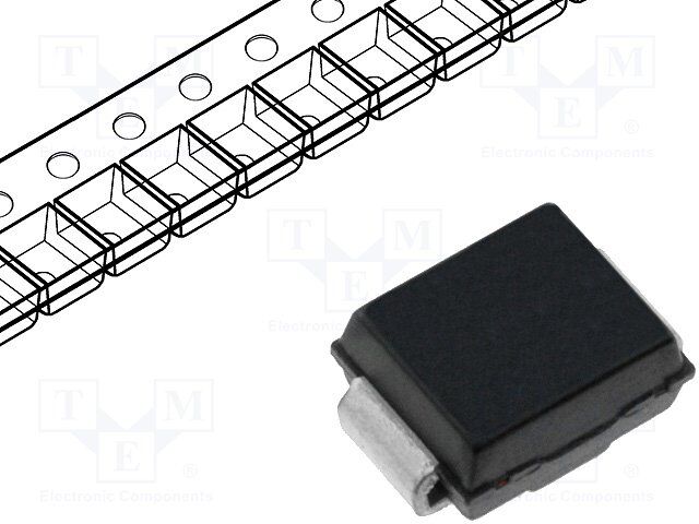
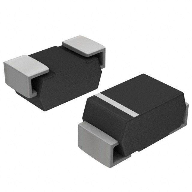
| 描述 | DIODE SCHOTTKY 30V 2A SMB肖特基二极管与整流器 2a/30V Schottky |
| 产品分类 | 单二极管/整流器分离式半导体 |
| 品牌 | Fairchild Semiconductor |
| 产品手册 | |
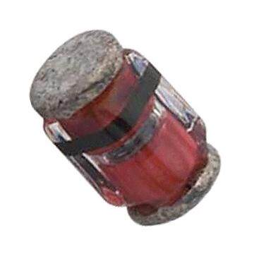
| 产品图片 |
|
| rohs | RoHS 合规性豁免无铅 / 符合限制有害物质指令(RoHS)规范要求 |
| 产品系列 | 二极管与整流器,肖特基二极管与整流器,Fairchild Semiconductor SS23- |
| 数据手册 | |
| 产品型号 | SS23 |
| 不同If时的电压-正向(Vf) | 500mV @ 2A |
| 不同 Vr、F时的电容 | - |
| 不同 Vr时的电流-反向漏电流 | 400µA @ 30V |
| 二极管类型 | |
| 产品 | Schottky Rectifiers |
| 产品目录页面 | |
| 产品种类 | 肖特基二极管与整流器 |
| 供应商器件封装 | DO-214AA(SMB) |
| 其它名称 | SS23CT |
| 包装 | 剪切带 (CT) |
| 单位重量 | 180 mg |
| 反向恢复时间(trr) | - |
| 商标 | Fairchild Semiconductor |
| 安装类型 | 表面贴装 |
| 安装风格 | SMD/SMT |
| 封装 | Reel |
| 封装/外壳 | DO-214AA,SMB |
| 封装/箱体 | SMB (DO-214AA) |
| 峰值反向电压 | 30 V |
| 工作温度-结 | -65°C ~ 125°C |
| 工作温度范围 | - 65 C to + 125 C |
| 工厂包装数量 | 3000 |
| 技术 | Silicon |
| 最大反向漏泄电流 | 400 uA |
| 最大工作温度 | + 125 C |
| 最大浪涌电流 | 50 A |
| 最小工作温度 | - 65 C |
| 标准包装 | 1 |
| 正向电压下降 | 0.5 V |
| 正向连续电流 | 2 A |
| 热阻 | 75°C/W Ja |
| 电压-DC反向(Vr)(最大值) | 30V |
| 电流-平均整流(Io) | 2A |
| 系列 | SS23 |
| 速度 | 快速恢复 =< 500 ns,> 200mA(Io) |
| 配置 | Single |
| 零件号别名 | SS23_NL |


- 商务部:美国ITC正式对集成电路等产品启动337调查
- 曝三星4nm工艺存在良率问题 高通将骁龙8 Gen1或转产台积电
- 太阳诱电将投资9.5亿元在常州建新厂生产MLCC 预计2023年完工
- 英特尔发布欧洲新工厂建设计划 深化IDM 2.0 战略
- 台积电先进制程称霸业界 有大客户加持明年业绩稳了
- 达到5530亿美元!SIA预计今年全球半导体销售额将创下新高
- 英特尔拟将自动驾驶子公司Mobileye上市 估值或超500亿美元
- 三星加码芯片和SET,合并消费电子和移动部门,撤换高东真等 CEO
- 三星电子宣布重大人事变动 还合并消费电子和移动部门
- 海关总署:前11个月进口集成电路产品价值2.52万亿元 增长14.8%


PDF Datasheet 数据手册内容提取
SS12 THRU SS1200 Reverse Voltage - 20 to 200 Volts Forward Current - 1.0 Ampere SURFACE MOUNT SCHOTTKY BARRIER RECTIFIER Features DO-214AC/SMA The plastic package carries Underwriters Laboratory Flammability Classification 94V-0 For surface mounted applications Metal silicon junction,majority carrier conduction 0.067 (1.70) 0.110(2.80) 0.039 (1.00) 0.094(2.40) Low power loss,high efficiency Built-in strain relief,ideal for automated placement High forward surge current capability 0.177(4.50) 0.157(3.99) High temperature soldering guaranteed: 0.012(0.305) 0.006(0.152) 250 °C/10 seconds at terminals 0.087(2.20) 0.078(1.90) Mechanical Data 0.059(1.50) 0.035(0.90) 0.008(0.203)MAX. Cas e : JEDEC DO-214AC/SMA molded plastic body 0.205(5.20) Termina ls : Solderable per MIL-STD-750,Method 2026 0.188(4.80) Po larity : Color band denotes cathode end Moun ting Po s ition : Any Weigh t : 0.002 ounce, 0.07 grams Dimensions in inches and (millimeters) Maximum Ratings And Electrical Characteristics Ratings at 25 C ambient temperature unless otherwise specified. Single phase half-wave 60Hz,resistive or inductive load,for capacitive load current derate by 20%. Parameter SS12 SS13 SS14 SS15 SS16 SS18 SS110 SS1150 SS1200 SYMBOLS UNITS MDD MDD MDD MDD MDD MDD MDD MDD MDD Marking Code SS12 SS13 SS14 SS15 SS16 SS18 SS110 SS1150 SS1200 Maximum repetitive peak reverse voltage VRRM 20 30 40 50 60 80 100 150 200 V Maximum RMS voltage VRMS 14 21 28 35 42 56 70 105 140 V Maximum DC blocking voltage VDC 20 30 40 50 60 80 100 150 200 V Maximum average forward rectified current I(AV) 1.0 A at TL(see fig.1) Peak forward surge current 8.3ms single half sine-wave IFSM 30 A superimposed onrated load (JEDEC Method) Maximum instantaneous forward voltage at 1.0A VF 0.45 0.55 0.70 0.85 0.9 V Maximum DC reverse current TA=25℃ 0.5 0.2 at rated DCblocking voltage TA=125℃ IR 10.0 5.0 2.0 mA Typical junction capacitance (NOTE 1) CJ 110 90 pF Typical thermal resistance (NOTE 2) RθJA 88.0 ℃/W Operating junction temperature range TJ -50 to +125 -50 to +150 ℃ Storage temperature range TSTG -50 to +150 ℃ Note:1.Measured at 1MHz and applied reverse voltage of 4.0V D.C. 2.P.C.B. mounted with 0.2x0.2”(5.0x5.0mm) copper pad areas DN:T20515A0 http://www.microdiode.com Rev:2020A0 Page :1
SS12 THRU SS1200 Reverse Voltage - 20 to 200 Volts Forward Current - 1.0 Ampere Typical Characterisitics Fig.1 Forward Current Derating Curve Fig.2 Typical Reverse Characteristics ent (A) 1.5 ent ( μA) 1100 43 TJ=100°C urr 1.0 urr C C ward erse 10 2 TJ=75°C v e For 0.5 s Re 101 SSSS1162-/SSSS112040 ag ou TJ=25°C er Single phase half-wave 60 Hz ne Av 0.0 resistive or inductive load sta 10 0 n 25 50 75 100 125 150 I 0 20 40 60 80 100 Case Temperature (°C) Percent of Rated Peak Reverse Voltage(%) Fig.3 Typical Forward Characteristic Fig.4 Typical Junction Capacitance A) 20 500 nt ( 10 F) TJ=25°C e p 200 urr e ( C c d an 100 war acit staneous For 10..01 SSSSSSSS11112116/05/SS//SSSSSS1114181 2 20 Junction Cap 521000 SSSS1162-/SSSS112400 n I 0 0.2 0.4 0.6 0.8 1.0 1.2 1.4 1.6 1.8 0.1 1 10 100 Instaneous Forward Voltage (V) Reverse Voltage (V) Fig.5 Maximum Non-Repetitive Peak Fig.6- Typical Transient Thermal Impedance Forward Surge Current ) W Current (A) 332604 °C(dance/ 100 e e g p d Sur 18 al Im 10 war 12 erm or h F T Peak 8(J.3E DmEsC S Mingelteh oHda)l f Sine Wave sient 00 n 1 1 10 100 Tra 0.01 0.1 1 10 100 Number of Cycles at 60Hz t, Pulse Duration(sec) The curve above is for reference only. http://www.microdiode.com Rev:2020A0 Page :2
SS12 THRU SS1200 Reverse Voltage - 20 to 200 Volts Forward Current - 1.0 Ampere Packing information unit:mm P0 Item Symbol Tolerance SMA P1 D1 d Carrier width A 0.1 2.80 E Carrier length B 0.1 5.33 F W1 Carrier depth C 0.1 2.36 W Sprocket hole d 0.05 1.50 B 13" Reel outside diameter D 2.0 330.00 13" Reel inner diameter D1 min 50.00 7" Reel outside diameter D 2.0 178.00 A P 7" Reel inner diameter D1 min 62.00 Feed hole diameter D2 0.5 13.00 Sprocket hole position E 0.1 1.75 Punch hole position F 0.1 5.50 D2 Punch hole pitch P 0.1 4.00 T Sprocket hole pitch P0 0.1 4.00 Embossment center P1 0.1 2.00 C Overall tape thickness T 0.1 0.28 Tape width W 0.3 12.00 D Reel width W1 1.0 18.00 Note:Devices are packed in accor dance with EIA standar RS-481-A and specifications listed above. Reel packing COMPONENT INNER REEL CARTON APPROX. PACKAGE REEL SIZE REEL SPACING BOX BOX DIA, SIZE CARTON GROSS WEIGHT (pcs) (m/m) (pcs) (m/m) (m/m) (m/m) (pcs) (kg) SMA 7" 2,000 4.0 4,000 183*155*183 178 382*356*392 80,000 16.0 SMA 11" 5,000 4.0 10,000 290*290*38 330 310*310*360 80,000 11.0 SMA 13" 7,500 4.0 15,000 335*335*38 330 350*330*360 120,000 14.5 Suggested Pad Layout Symbol Unit (mm) Unit (inch) A 1.68 0.066 B 1.52 0.060 C 3.90 0.154 D 2.41 0.095 E 5.45 0.215 Important Notice and Disclaimer Microdiode Electronics (Jiangsu) reserves the right to make changes to this document and its products and specifications at any time without notice. Customers should obtain and confirm the latest product information and specifications before final design,purchase or use. Microdiode Electronics (Jiangsu) makes no warranty, representation or guarantee regarding the suitability of its products for any particular purpose, not does Microdiode Electronics (Jiangsu) assume any liability for application assistance or customer product design. Microdiode Electronics (Jiangsu) does not warrant or accept any liability with products which are purchased or used for any unintended or unauthorized application. No license is granted by implication or otherwise under any intellectual property rights of Microdiode Electronics (Jiangsu). Microdiode Electronics (Jiangsu) products are not authorized for use as critical components in life support devices or systems without express written approval of Microdiode Electronics (Jiangsu). http://www.microdiode.com Rev:2020A0 Page :3