ICGOO在线商城 > SPU04N60C3
 Datasheet下载
- 型号: SPU04N60C3
- 制造商: Infineon
- 库位|库存: xxxx|xxxx
- 要求:
| 数量阶梯 | 香港交货 | 国内含税 |
| +xxxx | $xxxx | ¥xxxx |
查看当月历史价格
查看今年历史价格
SPU04N60C3产品简介:
ICGOO电子元器件商城为您提供SPU04N60C3由Infineon设计生产,在icgoo商城现货销售,并且可以通过原厂、代理商等渠道进行代购。 提供SPU04N60C3价格参考以及InfineonSPU04N60C3封装/规格参数等产品信息。 你可以下载SPU04N60C3参考资料、Datasheet数据手册功能说明书, 资料中有SPU04N60C3详细功能的应用电路图电压和使用方法及教程。
| 参数 | 数值 |
| 产品目录 | |
| ChannelMode | Enhancement |
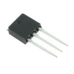
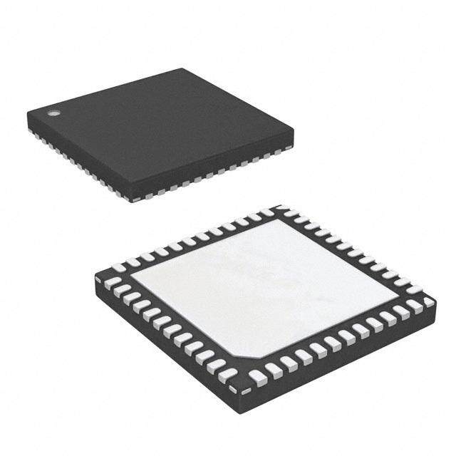
| 描述 | MOSFET N-CH 650V 4.5A TO-251MOSFET COOL MOS N-CH 650V 4.5A |
| 产品分类 | FET - 单分离式半导体 |
| FET功能 | 标准 |
| FET类型 | MOSFET N 通道,金属氧化物 |
| Id-ContinuousDrainCurrent | 4.5 A |
| Id-连续漏极电流 | 4.5 A |
| 品牌 | Infineon Technologies |
| 产品手册 | |
| 产品图片 |
|
| rohs | 符合RoHS无铅 / 符合限制有害物质指令(RoHS)规范要求 |
| 产品系列 | 晶体管,MOSFET,Infineon Technologies SPU04N60C3CoolMOS™ |
| 数据手册 | http://www.infineon.com/dgdl/SPD_U04N60C3_Rev.2.4.pdf?folderId=db3a304412b407950112b408e8c90004&fileId=db3a304412b407950112b42d7d034887 |
| 产品型号 | SPU04N60C3 |
| Pd-PowerDissipation | 50 W |
| Pd-功率耗散 | 50 W |
| RdsOn-Drain-SourceResistance | 950 mOhms |
| RdsOn-漏源导通电阻 | 950 mOhms |
| Vds-Drain-SourceBreakdownVoltage | 600 V |
| Vds-漏源极击穿电压 | 600 V |
| Vgs-Gate-SourceBreakdownVoltage | +/- 20 V |
| Vgs-栅源极击穿电压 | 20 V |
| 上升时间 | 2.5 ns |
| 下降时间 | 9.5 ns |
| 不同Id时的Vgs(th)(最大值) | 3.9V @ 200µA |
| 不同Vds时的输入电容(Ciss) | 490pF @ 25V |
| 不同Vgs时的栅极电荷(Qg) | 25nC @ 10V |
| 不同 Id、Vgs时的 RdsOn(最大值) | 950 毫欧 @ 2.8A,10V |
| 产品培训模块 | http://www.digikey.cn/PTM/IndividualPTM.page?site=cn&lang=zhs&ptm=25318 |
| 产品种类 | MOSFET |
| 供应商器件封装 | PG-TO251-3 |
| 其它名称 | SP000095850 |
| 典型关闭延迟时间 | 58.5 ns |
| 功率-最大值 | 50W |
| 包装 | 管件 |
| 商标 | Infineon Technologies |
| 商标名 | CoolMOS |
| 安装类型 | 通孔 |
| 安装风格 | SMD/SMT |
| 封装 | Tube |
| 封装/外壳 | TO-251-3 长引线,IPak,TO-251AB |
| 封装/箱体 | IPAK-3 |
| 工厂包装数量 | 1500 |
| 晶体管极性 | N-Channel |
| 最大工作温度 | + 150 C |
| 最小工作温度 | - 55 C |
| 标准包装 | 1,500 |
| 漏源极电压(Vdss) | 650V |
| 电流-连续漏极(Id)(25°C时) | 4.5A (Tc) |
| 系列 | SPU04N60 |
| 通道模式 | Enhancement |
| 配置 | Single |
| 零件号别名 | SP000095850 SPU04N60C3BKMA1 |


- 商务部:美国ITC正式对集成电路等产品启动337调查
- 曝三星4nm工艺存在良率问题 高通将骁龙8 Gen1或转产台积电
- 太阳诱电将投资9.5亿元在常州建新厂生产MLCC 预计2023年完工
- 英特尔发布欧洲新工厂建设计划 深化IDM 2.0 战略
- 台积电先进制程称霸业界 有大客户加持明年业绩稳了
- 达到5530亿美元!SIA预计今年全球半导体销售额将创下新高
- 英特尔拟将自动驾驶子公司Mobileye上市 估值或超500亿美元
- 三星加码芯片和SET,合并消费电子和移动部门,撤换高东真等 CEO
- 三星电子宣布重大人事变动 还合并消费电子和移动部门
- 海关总署:前11个月进口集成电路产品价值2.52万亿元 增长14.8%


(B)(TU)-VG.jpg)
PDF Datasheet 数据手册内容提取
IPB90R340C3 CoolMOS™ Power Transistor ProductSummary Features V @T =25°C 900 V DS J •Lowestfigure-of-meritR xQ ON g R @T =25°C 0.34 W DS(on),max J •Extremedv/dtrated Q 94 nC g,typ •Highpeakcurrentcapability •QualifiedaccordingtoJEDEC1) forindustrialapplications PG-TO263 •Pb-freeleadplating;RoHScompliant •Ultralowgatecharge CoolMOS™900Visdesignedfor: •QuasiResonantFlyback/Forwardtopologies •SMPS •PCSilverbox •Lighting •Solar TTyyppee PPaacckkaaggee MMaarrkkiinngg IIPPBB9900RR334400CC33 PPGG--TTOO226633 99RR334400CC Maximumratings,atT =25°C,unlessotherwisespecified J Parameter Symbol Conditions Value Unit Continuousdraincurrent I T =25 °C 15 A D C T =100 °C 9.5 C Pulseddraincurrent2) ID,pulse TC=25 °C 34 Avalancheenergy,singlepulse E I =3.1 A,V =50 V 678 mJ AS D DD Avalancheenergy,repetitivet 2),3) E I =3.1 A,V =50 V 1 AR AR D DD Avalanchecurrent,repetitivet 2),3) I 3.1 A AR AR MOSFETdv/dt ruggedness dv/dt V =0...400 V 50 V/ns DS Gatesourcevoltage V static ±20 V GS AC(f>1Hz) ±30 Powerdissipation P T =25 °C 208 W tot C Operatingandstoragetemperature T ,T -55...150 °C J stg RReevv..22..00 ppaaggee11 22001122--0044--1166
IPB90R340C3 Maximumratings,atT =25°C,unlessotherwisespecified J Parameter Symbol Conditions Value Unit Continuousdiodeforwardcurrent I 9.2 A S T =25 °C C Diodepulsecurrent2) IS,pulse 34 Reversediodedv/dt 4) dv/dt 4 V/ns Parameter Symbol Conditions Values Unit min. typ. max. Thermalcharacteristics Thermalresistance,junction-case R - - 0.6 K/W thJC SMDversion,device R onPCB:atminimum - - 62 thJA Thermalresistance,junction- footprint ambient SMDversion,device R onPCB:at6cm² - 35 - thJA ccoooolliinnggaarreeaa5) Solderingtemperature,onlyreflow solderingallowed;partnotqualified T reflowMSL1 - - 260 °C fordirectwavesolderingbutbottom sold sidePCBwavesolderingisallowed Electricalcharacteristics,atT =25°C,unlessotherwisespecified J Staticcharacteristics Drain-sourcebreakdownvoltage V V =0 V,I =250 µA 900 - - V (BR)DSS GS D Gatethresholdvoltage V V =V ,I =1 mA 2.5 3 3.5 GS(th) DS GS D V =900 V,V =0 V, Zerogatevoltagedraincurrent I DS GS - - 2 µA DSS T =25 °C j V =900 V,V =0 V, DS GS - 20 - T =150 °C j Gate-sourceleakagecurrent I V =20 V,V =0 V - - 100 nA GSS GS DS V =10 V,I =9.2 A, Drain-sourceon-stateresistance R GS D - 0.28 0.34 W DS(on) T =25 °C j V =10 V,I =9.2 A, GS D - 0.76 - T =150 °C j Gateresistance R f=1 MHz,opendrain - 1.3 - W G RReevv..22..00 ppaaggee22 22001122--0044--1166
IPB90R340C3 Parameter Symbol Conditions Values Unit min. typ. max. Dynamiccharacteristics Inputcapacitance C - 2400 - pF iss V =0 V,V =100 V, GS DS f=1 MHz Outputcapacitance C - 120 - oss Effectiveoutputcapacitance,energy C - 71 - related6) o(er) V =0 V,V =0 V GS DS Effectiveoutputcapacitance,time to 500 V C - 280 - related7) o(tr) Turn-ondelaytime t - 70 - ns d(on) V =400 V, Risetime t DD - 20 - r V =10 V,I =9.2A, GS D Turn-offdelaytime td(off) RG=23.1 W - 400 - Falltime t - 25 - f GateChargeCharacteristics Gatetosourcecharge Q - 11 - nC gs Gatetodraincharge Qgd VDD=400 V,ID=9.2 A, - 41 - Gatechargetotal Qg VGS=0 to 10 V - 94 - Gateplateauvoltage V - 4.6 - V plateau ReverseDiode V =0 V,I =9.2 A, Diodeforwardvoltage V GS F - 0.8 1.2 V SD T =25 °C j Reverserecoverytime t - 510 - ns rr V =400 V,I =I , Reverserecoverycharge Q R F S - 11 - µC rr di /dt=100 A/µs F Peakreverserecoverycurrent I - 41 - A rrm 1)J-STD20andJESD22 2)Pulsewidtht limitedbyT p J,max 3)RepetitiveavalanchecausesadditionalpowerlossesthatcanbecalculatedasP =E *f. AV AR 4)I ≤I , di/dt≤200A/µs, V =400V,V <V ,T<T ,identicallowsideandhighsideswitch SD D DClink peak (BR)DSS J J,max 5)Deviceon40mm*40mm*1.5mmepoxyPCBFR4with6cm²(onelayer,70µmthick)copperareafordrain connection.PCBisverticalwithoutblownair. 6)C isafixedcapacitancethatgivesthesamestoredenergyasC whileV isrisingfrom0to50%V . o(er) oss DS DSS 7)C isafixedcapacitancethatgivesthesamechargingtimeasC whileV isrisingfrom0to50%V o(tr) oss DS DSS. RReevv..22..00 ppaaggee33 22001122--0044--1166
IPB90R340C3 1Powerdissipation 2Safeoperatingarea P =f(T ) I =f(V );T =25°C;D=0 tot C D DS C parameter:t p 225500 110022 lliimmiitteeddbbyyoonn--ssttaattee rreessiissttaannccee 11µµss 220000 1100µµss 110011 110000µµss 115500 11mmss ]] WW [[ A]A] PPtottot I[I[DD 1100mmss 110000 110000 DDCC 5500 00 1100--11 00 2255 5500 7755 110000 112255 115500 11 1100 110000 11000000 TTCC[[°°CC]] VVDDSS[[VV]] 3Max.transientthermalimpedance 4Typ.outputcharacteristics Z =f(t ) I =f(V );T =25°C thJC P D DS J parameter:D=t /T parameter:V p GS 100 50 10V 8V 40 0.5 6V 30 W] 0.2 5.5V [K/ 10-1 [A] C D J 0.1 I h Zt 20 5V 0.05 0.02 0.01 10 4.5V singlepulse 4V 10-2 0 0 5 10 15 20 25 10-5 10-4 10-3 10-2 10-1 t [s] V [V] p DS RReevv..22..00 ppaaggee44 22001122--0044--1166
IPB90R340C3 5Typ.outputcharacteristics 6Typ.drain-sourceon-stateresistance I =f(V );T =150°C R =f(I );T =150°C D DS J DS(on) D J parameter:V parameter:V GS GS 2255 55 2200VV 1100VV 2200 88VV 44 66VV 55VV 1155 33 ]] 44..55VV WW [A][A] [[on)on) IIDD DS(DS( 1100VV RR 1100 22 55VV 44VV 44..88VV 55 11 44..55VV 44VV 00 00 00 55 1100 1155 2200 2255 00 55 1100 1155 2200 2255 3300 VV [[VV]] II [[AA]] DDSS DD 7Drain-sourceon-stateresistance 8Typ.transfercharacteristics R =f(T );I =9.2A;V =10V I =f(V );V =20V DS(on) j D GS D GS DS parameter:T J 1 50 25°C 0.8 40 0.6 30 ] W [n) 98% typ A] o [ S( D RD I 150°C 0.4 20 0.2 10 0 0 -60 -20 20 60 100 140 180 0 2 4 6 8 10 T [°C] V [V] J GS RReevv..22..00 ppaaggee55 22001122--0044--1166
IPB90R340C3 9Typ.gatecharge 10Forwardcharacteristicsofreversediode V =f(Q );I =9.2Apulsed I =f(V ) GS gate D F SD parameter:V parameter:T DD J 1100 110022 88 2255°°CC,,9988%% 115500°°CC,,9988%% 110011 66 115500°°CC [V][V] 440000VV 772200VV A]A] GSGS [[FF 2255°°CC VV II 44 110000 22 00 1100--11 00 2200 4400 6600 8800 110000 00 00..55 11 11..55 22 QQ [[nnCC]] VV [[VV]] ggaattee SSDD 11Avalancheenergy 12Drain-sourcebreakdownvoltage E =f(T );I =3.1A;V =50V V =f(T );I =0.25mA AS J D DD BR(DSS) J D 700 1050 600 1000 500 950 ] 400 V] J [ m S) [AS R(DS E 300 B V 900 200 850 100 0 800 25 50 75 100 125 150 -60 -20 20 60 100 140 180 T [°C] T [°C] J J RReevv..22..00 ppaaggee66 22001122--0044--1166
IPB90R340C3 13Typ.capacitances 14Typ.C storedenergy oss C=f(V );V =0V;f=1MHz E =f(V ) DS GS oss DS 110044 1122 CCiissss 1100 110033 88 ]] ]] JJ FF µµ pp 110022 CCoossss [[ 66 C[C[ ossoss EE 44 110011 CCrrssss 22 110000 00 00 110000 220000 330000 440000 550000 660000 00 110000 220000 330000 440000 550000 660000 VV [[VV]] VV [[VV]] DDSS DDSS RReevv..22..00 ppaaggee77 22001122--0044--1166
IPB90R340C3 Definitionofdiodeswitchingcharacteristics RReevv..22..00 ppaaggee88 22001122--0044--1166
IPB90R340C3 PG-TO263Outlines RReevv..22..00 ppaaggee99 22001122--0044--1166
IPB90R340C3 Publishedby InfineonTechnologiesAG 81726Munich,Germany ©2008InfineonTechnologiesAG AllRightsReserved. LegalDisclaimer Theinformationgiveninthisdocumentshallinnoeventberegardedasaguaranteeof conditionsorcharacteristics.Withrespecttoanyexamplesorhintsgivenherein,anytypical valuesstatedhereinand/oranyinformationregardingtheapplicationofthedevice, InfineonTechnologiesherebydisclaimsanyandallwarrantiesandliabilitiesofanykind, includingwithoutlimitation,warrantiesofnon-infringementofintellectualpropertyrights ofanythirdparty. Information Forfurtherinformationontechnology,deliverytermsandconditionsandprices,please contactthenearestInfineonTechnologiesOffice(www.infineon.com). Warnings Duetotechnicalrequirements,componentsmaycontaindangeroussubstances.Forinformation onthetypesinquestion,pleasecontactthenearestInfineonTechnologiesOffice. InfineonTechnologiescomponentsmaybeusedinlife-supportdevicesorsystemsonlywith theexpresswrittenapprovalofInfineonTechnologies,ifafailureofsuchcomponentscan rreeaassoonnaabbllyybbeeeexxppeecctteeddttooccaauusseetthheeffaaiilluurreeoofftthhaattlliiffee--ssuuppppoorrttddeevviicceeoorrssyysstteemmoorrttooaaffffeecctt thesafetyoreffectivenessofthatdeviceorsystem.Lifesupportdevicesorsystemsare intendedtobeimplantedinthehumanbodyortosupportand/ormaintainandsustain and/orprotecthumanlife.Iftheyfail,itisreasonabletoassumethatthehealthoftheuser orotherpersonsmaybeendangered. RReevv..22..00 ppaaggee1100 22001122--0044--1166
Mouser Electronics Authorized Distributor Click to View Pricing, Inventory, Delivery & Lifecycle Information: I nfineon: SPU04N60C3 IPB90R340C3ATMA1 IPB90R340C3 IPW80R290C3A IPB80R290C3A