 Datasheet下载
- 型号: SP4065-08ATG
- 制造商: Littelfuse
- 库位|库存: xxxx|xxxx
- 要求:
| 数量阶梯 | 香港交货 | 国内含税 |
| +xxxx | $xxxx | ¥xxxx |
查看当月历史价格
查看今年历史价格
SP4065-08ATG产品简介:
ICGOO电子元器件商城为您提供SP4065-08ATG由Littelfuse设计生产,在icgoo商城现货销售,并且可以通过原厂、代理商等渠道进行代购。 SP4065-08ATG价格参考。LittelfuseSP4065-08ATG封装/规格:TVS - 二极管, 。您可以下载SP4065-08ATG参考资料、Datasheet数据手册功能说明书,资料中有SP4065-08ATG 详细功能的应用电路图电压和使用方法及教程。
Littelfuse Inc.生产的SP4065-08ATG是一款TVS(瞬态电压抑制)二极管,主要用于保护电子设备免受瞬态电压的损害。其应用场景包括:

1. 数据接口保护:适用于USB、HDMI、以太网等高速数据接口,能够有效抑制静电放电(ESD)和浪涌电压,确保信号传输的稳定性。

2. 通信设备:在手机、路由器、调制解调器等通信设备中,该TVS二极管可保护敏感元件免受雷击浪涌和开关噪声的影响。

3. 汽车电子:用于车载信息娱乐系统、导航设备和传感器电路中,提供可靠的过电压保护,满足汽车环境中严苛的电磁兼容性要求。

4. 工业控制:在自动化控制系统、PLC模块和传感器接口中,防止因感应雷击或负载切换引起的电压尖峰对设备造成损坏。

5. 消费类电子产品:如笔记本电脑、平板电脑和数码相机等,为电源输入端和外部连接器提供保护,提升产品可靠性。

SP4065-08ATG具有低电容特性,适合高速信号线路;同时具备高响应速度和良好的钳位性能,能够在微秒级时间内将瞬态电压限制在安全范围内,从而保护后端电路不受损害。
| 参数 | 数值 |
| 品牌 | Littelfuse |
| 产品目录 | 半导体 |
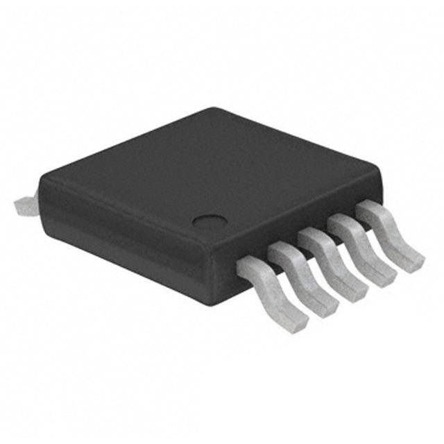
| 描述 | TVS二极管阵列 3.3V 20A Lightning Surge Prot |
| 产品分类 | 分离式半导体 |
| 产品手册 | |
| 产品图片 |
|
| 产品系列 | 二极管与整流器,TVS二极管,TVS二极管阵列,Littelfuse SP4065-08ATG |
| mouser_ship_limit | 该产品可能需要其他文件才能进口到中国。 |
| 产品型号 | SP4065-08ATG |
| 产品种类 | TVS二极管阵列 |
| 商标 | Littelfuse |
| 商标名 | SPA |
| 外壳高度 | 1.25 mm |
| 安装风格 | SMD/SMT |
| 封装 | Reel |
| 封装/箱体 | MSOP-10 |
| 尺寸 | 3.1 mm W x 3.1 mm L x 1.1 mm H |
| 峰值浪涌电流 | 20 A |
| 峰值脉冲功率耗散 | 300 W |
| 工作电压 | 3.3 V |
| 最大工作温度 | + 125 C |
| 最小工作温度 | - 40 C |
| 极性 | Unidirectional |
| 电容 | 4.4 pF |
| 端接类型 | SMD/SMT |
| 通道 | 8 Channels |
| 钳位电压 | 13.5 V |


- 商务部:美国ITC正式对集成电路等产品启动337调查
- 曝三星4nm工艺存在良率问题 高通将骁龙8 Gen1或转产台积电
- 太阳诱电将投资9.5亿元在常州建新厂生产MLCC 预计2023年完工
- 英特尔发布欧洲新工厂建设计划 深化IDM 2.0 战略
- 台积电先进制程称霸业界 有大客户加持明年业绩稳了
- 达到5530亿美元!SIA预计今年全球半导体销售额将创下新高
- 英特尔拟将自动驾驶子公司Mobileye上市 估值或超500亿美元
- 三星加码芯片和SET,合并消费电子和移动部门,撤换高东真等 CEO
- 三星电子宣布重大人事变动 还合并消费电子和移动部门
- 海关总署:前11个月进口集成电路产品价值2.52万亿元 增长14.8%


PDF Datasheet 数据手册内容提取
TVS Diode Arrays (SPA ® Diodes) Lightning Surge Protection - SP4065 SP4065 Series 3.3V 20A Diode Array RoHS Pb GREEN Description The SP4065 integrates low capacitance diodes with an additional zener diode to protect each I/O pin against ESD and high surge events. This robust device can safely absorb up to 20A per IEC 61000-4-5, 2nd Edition (tp=8/20μs) without performance degradation and a minimum ±30kV ESD per IEC 61000-4-2 International Standard. Their low loading capacitance also makes them ideal for protecting highspeed signal pins. Pinout Features • ESD, IEC 61000-4-2, • Low leakage current of I/O 1 I/O 8 ±30kV contact, ±30kV air 1µA (MAX) at 3.3V I/O 2 I/O 7 • EFT, IEC 61000-4-4, 40A • AEC-Q101 qualified I/O 6 (5/50ns) • Halogen free, Lead-free I/O 3 • Lightning, IEC 61000-4-5, and RoHS compliant I/O 5 I/O 4 2nd Edition 20A (8/20µs) • Moisture Sensitivity Level NC GND • Low capacitance of 4.4pF (MSL - Level 1) (TYP) per I/O Functional Block Diagram Applications • LCD/LED TVs • Notebooks I/O 8 I/O 7 I/O 6 I/O 5 • Desktops • 1Gb Ethernet • Game Consoles • Network Hardware • Set Top Boxes • Small Cells Application Example LVDS Interface LVDS Controller I/O 1 I/O 2 I/O 3 I/O 4 GND CLK+ CLK- A0+ Additional Information A0- Outside World A1+ A1- A2+ A2- Datasheet Resources Samples Signal Shield GND SP4065-08ATG Life Support Note: Shield GND Not Intended for Use in Life Support or Life Saving Applications The products shown herein are not designed for use in life sustaining or life saving applications unless otherwise expressly indicated. © 2016 Littelfuse, Inc. Specifications are subject to change without notice. Revised: 12/29/16
TVS Diode Arrays (SPA ® Diodes) Lightning Surge Protection - SP4065 Absolute Maximum Ratings Thermal Information Symbol Parameter Value Units Parameter Rating Units I Peak Current (t=8/20μs) 20.0 A Storage Temperature Range -55 to 150 °C PP p Maximum Junction Temperature 150 °C P Peak Pulse Power (t=8/20µs) 300 W PK p Maximum Lead Temperature 260 °C T Operating Temperature -40 to 125 ºC OP (Soldering 20-40s) T Storage Temperature -55 to 150 °C STOR CAUTION: Stresses above those listed in “Absolute Maximum Ratings” may cause permanent damage to the device. This is a stress only rating and operation of the device at these or any other conditions above those indicated in the operational sections of this specification is not implied. Electrical Characteristics (T =25ºC) OP Parameter Symbol Test Conditions Min Typ Max Units Reverse Standoff Voltage V 3.3 V RWM Snap Back Voltage V I =50mA 2.8 V SB SB Reverse Leakage Current I V =3.3V, I/O to GND 0.5 1.0 µA LEAK R I =1A, t=8/20µs, Fwd 5.5 V PP p I =5A, t=8/20µs, Fwd 7.0 V Clamp Voltage1 V PP p C I =10A, t=8/20µs, Fwd 9.0 V PP p I =20A, t=8/20µs, Fwd 13.5 V PP p Dynamic Resistance R (V - V ) / (I - I ) 0.4 Ω DYN C2 C1 PP2 PP1 IEC61000-4-2 (Contact) ±30 kV ESD Withstand Voltage1 V ESD IEC61000-4-2 (Air) ±30 kV Diode Capacitance1 C Reverse Bias=0V 4.4 5.0 pF I/O-GND Diode Capacitance1 C Reverse Bias=0V 2.2 pF I/O-I/O Note: 1. Parameter is guaranteed by design and/or device characterization. Clamping Voltage vs. I Capacitance vs. Bias PP 14.0 5.0 12.0 4.0 V)C10.0 pF) Clamp Voltage ( 68..00 Capacitance ( 23..00 4.0 1.0 2.0 0.0 0.0 1.0 3.0 5.0 7.0 9.0 11.0 13.0 15.0 17.0 19.0 21.0 0 0.5 1 1.5 2 2.5 3 Peak Pulse Current-IPP (A) Bias Voltage (V) © 2016 Littelfuse, Inc. Specifications are subject to change without notice. Revised: 12/29/16
TVS Diode Arrays (SPA ® Diodes) Lightning Surge Protection - SP4065 8/20µs Pulse Waveform Product Characteristics 110% Lead Plating Pre-Plated Frame 100% Lead Material Copper Alloy 90% 80% Lead Coplanarity 0.0004 inches (0.102mm) of IPP 70% Substrate material Silicon nt 60% e erc 50% Body Material Molded Epoxy, rated UL 94 V-0 P 40% 30% 20% Notes : 1. All dimensions are in millimeters 10% 2. Dimensions include solder plating. 0% 0.0 5.0 10.0 15.0 20.0 25.0 30.0 3. Dimensions are exclusive of mold flash & metal burr. Time (μs) 4. Blo is facing up for mold and facing down for trim/form, i.e. reverse trim/form. 5. Package surface matte finish VDI 11-13. Soldering Parameters tP Reflow Condition Pb – Free assembly TP CCrriittiiccaall ZZoonnee e RRaammpp--uupp TTLL ttoo TTPP Pre Heat --- TTTeeimmmepp ee(mrraaittnuu rrteeo MMmaainxx ) ( (T(Ttss(m()mina)x))) 1625000 0–°° CC1 80 secs rutarepm TS(mTaxL) tL RRaammpp--ddoown s e PPrreehheeaatt T Atov epreaagke ramp up rate (Liquidus) Temp (TL) 3°C/second max TS(min) tS T to T - Ramp-up Rate 3°C/second max S(max) L 25 - Temperature (T) (Liquidus) 217°C time to peak temperature Time Reflow L - Temperature (t) 60 – 150 seconds L Peak Temperature (T) 260+0/-5 °C Part Numbering System P Time within 5°C of actual peak 20 – 40 seconds SP 4065 -08ATG Temperature (t) p G= Green Ramp-down Rate 6°C/second max TVS Diode Arrays (SPA® Diodes) T= Tape & Reel Time 25°C to peak Temperature (T) 8 minutes Max. P Do not exceed 260°C Package Series A = MSOP10 Number of Channels Ordering Information Part Marking System Part Number Package Marking Min. Order Qty. LF SP4065-08ATG MSOP-10 AAH8 4000 YYWWD YYWW = Date code Product Series AA*8 Number of AA= SP4065 Channels Assembly Site © 2016 Littelfuse, Inc. Specifications are subject to change without notice. Revised: 12/29/16
TVS Diode Arrays (SPA ® Diodes) Lightning Surge Protection - SP4065 Package Dimensions — MSOP-10 2.00 D [0.0787] 0.50 Package MSOP 10 [0.0197] Pins 10 JEDEC MO-187 Millimeters Inches E1 E 5.28[0.2079]3.20[0.1260] 1.04[0.0409]4.24[0.1669] DAIM M-in M1.1a0x M-in 0M.0a4x3 A1 0.00 0.15 0.000 0.006 B 0.17 0.27 0.007 0.011 0.32 [0.0126] c 0.08 0.23 0.003 0.009 Solder Pad Layout D 2.90 3.10 0.114 0.122 1 2 A E 4.67 5.10 0.184 0.200 E1 2.90 3.10 0.114 0.122 C e 0.50 BSC 0.020 BSC L 0.40 0.80 0.016 0.032 B e A1 L Embossed Carrier Tape & Reel Specification — MSOP-10 Millimetres Inches Min Max Min Max E 1.65 1.85 0.065 0.073 e 0.5 0.02 F 5.40 5.60 0.213 0.220 D 1.50 1.60 0.059 0.063 D1 1.50 Min 0.059 Min P0 3.90 4.10 0.154 0.161 W 11.70 12.30 0.460 0.484 P 7.90 8.10 0.311 0.319 A0 5.20 5.40 0.205 0.213 B0 3.20 3.50 0.126 0.138 K0 1.20 1.50 0.047 0.059 t 0.30 +/- 0.05 0.012+/- 0.002 Pin 1 Location User Feeding Direction © 2016 Littelfuse, Inc. Specifications are subject to change without notice. Revised: 12/29/16