ICGOO在线商城 > 集成电路(IC) > 接口 - 驱动器,接收器,收发器 > SN75ALS176D
 Datasheet下载
- 型号: SN75ALS176D
- 制造商: Texas Instruments
- 库位|库存: xxxx|xxxx
- 要求:
| 数量阶梯 | 香港交货 | 国内含税 |
| +xxxx | $xxxx | ¥xxxx |
查看当月历史价格
查看今年历史价格
SN75ALS176D产品简介:
ICGOO电子元器件商城为您提供SN75ALS176D由Texas Instruments设计生产,在icgoo商城现货销售,并且可以通过原厂、代理商等渠道进行代购。 SN75ALS176D价格参考¥7.24-¥10.64。Texas InstrumentsSN75ALS176D封装/规格:接口 - 驱动器,接收器,收发器, 半 收发器 1/1 RS422,RS485 8-SOIC。您可以下载SN75ALS176D参考资料、Datasheet数据手册功能说明书,资料中有SN75ALS176D 详细功能的应用电路图电压和使用方法及教程。
Texas Instruments 的 SN75ALS176D 是一款 低功耗、半双工差分收发器,常用于 RS-485 通信接口中。它属于接口类器件中的驱动器/接收器/收发器类别,广泛应用于工业自动化、楼宇控制、仪器仪表等领域。

 主要应用场景包括:

1. 工业自动化系统:用于PLC(可编程逻辑控制器)、传感器、执行器之间的数据通信,支持长距离、抗干扰的信号传输。
2. 楼宇自动化:如暖通空调(HVAC)、照明控制、安防系统等,适用于需要多点通信和远距离传输的场合。
3. 电机控制与变频器通信:在工业电机控制系统中,作为主控制器与各从设备之间的通信接口。
4. 远程数据采集系统:适用于远程监控与数据采集(SCADA)系统,实现现场设备与中央控制系统的可靠通信。
5. 智能电表与能源管理系统:用于电力系统中电表之间的通信,支持 Modbus 或其他基于 RS-485 的协议。

该器件具有较强的抗干扰能力,支持多点通信结构,适用于电磁干扰较严重的工业环境。其半双工设计适合对成本和功耗有要求的应用场景。
| 参数 | 数值 |
| 产品目录 | 集成电路 (IC)半导体 |
| 描述 | IC DIFF BUS TRANSCEIVER 8-SOICRS-422/RS-485 接口 IC Differential Bus |
| Duplex | Half Duplex |
| 产品分类 | |
| 品牌 | Texas Instruments |
| 产品手册 | |
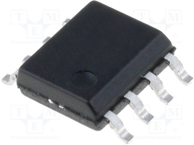
| 产品图片 |
|
| rohs | 符合RoHS无铅 / 符合限制有害物质指令(RoHS)规范要求 |
| 产品系列 | 接口 IC,RS-422/RS-485 接口 IC,Texas Instruments SN75ALS176D- |
| 数据手册 | |
| 产品型号 | SN75ALS176D |
| 产品目录页面 | |
| 产品种类 | RS-422/RS-485 接口 IC |
| 供应商器件封装 | 8-SOIC |
| 其它名称 | 296-9958-5 |
| 功能 | Transceiver |
| 包装 | 管件 |
| 协议 | RS422,RS485 |
| 单位重量 | 72.600 mg |
| 双工 | Half Duplex |
| 商标 | Texas Instruments |
| 安装类型 | 表面贴装 |
| 安装风格 | SMD/SMT |
| 封装 | Tube |
| 封装/外壳 | 8-SOIC(0.154",3.90mm 宽) |
| 封装/箱体 | SOIC-8 |
| 工作温度 | 0°C ~ 70°C |
| 工作温度范围 | 0 C to + 70 C |
| 工作电源电压 | 5 V |
| 工厂包装数量 | 75 |
| 接收器滞后 | 60mV |
| 接收机数量 | 4 Receiver |
| 数据速率 | 35 Mb/s |
| 最大工作温度 | + 70 C |
| 最小工作温度 | 0 C |
| 标准包装 | 75 |
| 激励器数量 | 1 Driver |
| 电压-电源 | 4.75 V ~ 5.25 V |
| 电源电流 | 30 mA |
| 类型 | 收发器 |
| 系列 | SN75ALS176 |
| 驱动器/接收器数 | 1/1 |


- 商务部:美国ITC正式对集成电路等产品启动337调查
- 曝三星4nm工艺存在良率问题 高通将骁龙8 Gen1或转产台积电
- 太阳诱电将投资9.5亿元在常州建新厂生产MLCC 预计2023年完工
- 英特尔发布欧洲新工厂建设计划 深化IDM 2.0 战略
- 台积电先进制程称霸业界 有大客户加持明年业绩稳了
- 达到5530亿美元!SIA预计今年全球半导体销售额将创下新高
- 英特尔拟将自动驾驶子公司Mobileye上市 估值或超500亿美元
- 三星加码芯片和SET,合并消费电子和移动部门,撤换高东真等 CEO
- 三星电子宣布重大人事变动 还合并消费电子和移动部门
- 海关总署:前11个月进口集成电路产品价值2.52万亿元 增长14.8%


PDF Datasheet 数据手册内容提取
SN65ALS176, SN75ALS176, SN75ALS176A, SN75ALS176B DIFFERENTIAL BUS TRANSCEIVERS SLLS040H – AUGUST 1987 – REVISED JUNE 2000 (cid:0) Meet or Exceed the Requirements of D OR P PACKAGE TIA/EIA-422-B, TIA/EIA-485-A† and ITU (TOP VIEW) Recommendations V.11 and X.27 (cid:0) R 1 8 VCC Operate at Data Rates up to 35 Mbaud RE 2 7 B (cid:0) Four Skew Limits Available: DE 3 6 A SN65ALS176...15 ns D 4 5 GND SN75ALS176...10 ns SN75ALS176A...7.5 ns SN75ALS176B...5 ns (cid:0) Designed for Multipoint Transmission on Long Bus Lines in Noisy Environments (cid:0) Low Supply-Current Requirements ...30 mA Max (cid:0) Wide Positive and Negative Input/Output Bus-Voltage Ranges (cid:0) Thermal Shutdown Protection (cid:0) Driver Positive and Negative Current Limiting (cid:0) Receiver Input Hysteresis (cid:0) Glitch-Free Power-Up and Power-Down Protection (cid:0) Receiver Open-Circuit Fail-Safe Design description The SN65ALS176 and SN75ALS176 series differential bus transceivers are designed for bidirectional data communication on multipoint bus transmission lines. They are designed for balanced transmission lines and meet TIA/EIA-422-B, TIA/EIA-485-A, and ITU Recommendations V.11 and X.27. The SN65ALS176 and SN75ALS176 series combine a 3-state, differential line driver and a differential input line receiver, both of which operate from a single 5-V power supply. The driver and receiver have active-high and active-low enables, respectively, that can be connected together externally to function as a direction control. The driver differential outputs and the receiver differential inputs are connected internally to form a differential input/output (I/O) bus port that is designed to offer minimum loading to the bus when the driver is disabled or V = 0. This port features wide positive and negative common-mode voltage ranges, making the device CC suitable for party-line applications. The SN65ALS176 is characterized for operation from –40°C to 85°C. The SN75ALS176 series is characterized for operation from 0°C to 70°C. Please be aware that an important notice concerning availability, standard warranty, and use in critical applications of TexasInstruments semiconductor products and disclaimers thereto appears at the end of this data sheet. †These devices meet or exceed the requirements of TIA/EIA-485-A, except for the Generator Contention Test (para. 3.4.2) and the Generator Current Limit (para. 3.4.3). The applied test voltage ranges are –6 V to 8 V for the SN75ALS176, SN75ALS176A, and SN75ALS176B and –4 V to 8 V for the SN65ALS180. PRODUCTION DATA information is current as of publication date. Copyright 2000, Texas Instruments Incorporated Products conform to specifications per the terms of Texas Instruments standard warranty. Production processing does not necessarily include testing of all parameters. POST OFFICE BOX 655303 • DALLAS, TEXAS 75265 1
SN65ALS176, SN75ALS176, SN75ALS176A, SN75ALS176B DIFFERENTIAL BUS TRANSCEIVERS SLLS040H – AUGUST 1987 – REVISED JUNE 2000 AVAILABLE OPTIONS PACKAGED DEVICES TA tsk(lim)†† SMALL OUTLINE PLASTIC DIP (D)‡ (P) 10 SN75ALS176D SN75ALS176P 0°C to 70°C 7.5 SN75ALS176AD SN75ALS176AP 5 SN75ALS176BD SN75ALS176BP –40°C to 85°C 15 SN65ALS176D SN65ALS176P †This is the maximum range that the driver or receiver delay times vary over temperature, VCC, and process (device to device). ‡The D package is available taped and reeled. Add the suffix R to the device type (e.g., SN75ALS176DR). Function Tables DRIVER INPUT ENABLE OUTPUTS D DE A B H H H L L H L H X L Z Z H = high level, L = low level, X = irrelevant, Z = high impedance RECEIVER DIFFERENTIAL ENABLE OUTPUT INPUTS RE R A–B VID ≥ 0.2 V L H –0.2 V < VID < 0.2 V L ? VID ≤ –0.2 V L L X H Z Inputs open L H H = high level, L = low level, X = irrelevant, Z = high impedance logic symbol§ logic diagram (positive logic) 3 DE 3 DE EN1 2 4 RE EN2 D 6 2 4 1 A RE D 1 7 B R 1 67 A Bus B 1 R 2 §This symbol is in accordance with ANSI/IEEE Std 91-1984 and IEC Publication 617-12. 2 POST OFFICE BOX 655303 • DALLAS, TEXAS 75265
SN65ALS176, SN75ALS176, SN75ALS176A, SN75ALS176B DIFFERENTIAL BUS TRANSCEIVERS SLLS040H – AUGUST 1987 – REVISED JUNE 2000 schematics of inputs and outputs EQUIVALENT OF EACH INPUT TYPICAL OF A AND B I/O PORTS TYPICAL OF RECEIVER OUTPUT VCC VCC VCC R(eq) 180 kW 8N5O WM NOM Connected on A Port Input 3 kW NOM A or B Output 18 kW NOM Driver Input: R(eq) = 3 kW NOM 180 kW Enable Inputs: R(eq) = 8 kW NOM NOM 1.1 kW R(eq) = equivalent resistor Connected NOM on B Port absolute maximum ratings over operating free-air temperature range (unless otherwise noted)† Supply voltage, V (see Note 1) . . . . . . . . . . . . . . . . . . . . . . . . . . . . . . . . . . . . . . . . . . . . . . . . . . . . . . . . . . . . . 7 V CC Voltage range at any bus terminal . . . . . . . . . . . . . . . . . . . . . . . . . . . . . . . . . . . . . . . . . . . . . . . . . . . . . –7 V to 12 V Enable input voltage, V . . . . . . . . . . . . . . . . . . . . . . . . . . . . . . . . . . . . . . . . . . . . . . . . . . . . . . . . . . . . . . . . . . . . 5.5 V I Package thermal impedance, q (see Note 2): D package . . . . . . . . . . . . . . . . . . . . . . . . . . . . . . . . . . . 97°C/W JA P package . . . . . . . . . . . . . . . . . . . . . . . . . . . . . . . . . . . 85°C/W Lead temperature 1,6 mm (1/16 inch) from case for 10 seconds . . . . . . . . . . . . . . . . . . . . . . . . . . . . . . . 260°C Storage temperature range, T . . . . . . . . . . . . . . . . . . . . . . . . . . . . . . . . . . . . . . . . . . . . . . . . . . . –65°C to 150°C stg †Stresses beyond those listed under “absolute maximum ratings” may cause permanent damage to the device. These are stress ratings only, and functional operation of the device at these or any other conditions beyond those indicated under “recommended operating conditions” is not implied. Exposure to absolute-maximum-rated conditions for extended periods may affect device reliability. NOTES: 1. All voltage values, except differential I/O bus voltage, are with respect to network ground terminal. 2. The package thermal impedance is calculated in accordance with JESD 51. POST OFFICE BOX 655303 • DALLAS, TEXAS 75265 3
SN65ALS176, SN75ALS176, SN75ALS176A, SN75ALS176B DIFFERENTIAL BUS TRANSCEIVERS SLLS040H – AUGUST 1987 – REVISED JUNE 2000 recommended operating conditions (unless otherwise noted) MIN NOM MAX UNIT Supply voltage, VCC 4.75 5 5.25 V 12 IInnppuutt vvoollttaaggee aatt aannyy bbuuss tteerrmmiinnaall ((sseeppaarraatteellyy oorr ccoommmmoonn mmooddee)), VVII oorr VVIICC VV –7 High-level input voltage, VIH D, DE, and RE 2 V Low-level input voltage, VIL D, DE, and RE 0.8 V Differential input voltage, VID (see Note 3) ±12 V Driver –60 mA HHiigghh-lleevveell oouuttppuutt ccuurrrreenntt, IIOOHH Receiver –400 m A Driver 60 LLooww-lleevveell oouuttppuutt ccuurrrreenntt, IIOOLL mmAA Receiver 8 SN65ALS176 –40 85 OOppeerraattiinngg ffrreeee-aaiirr tteemmppeerraattuurree, TTAA °°CC SN75ALS176 series 0 70 NOTE 3: Differential input/output bus voltage is measured at the noninverting terminal A with respect to the inverting terminal B. 4 POST OFFICE BOX 655303 • DALLAS, TEXAS 75265
SN65ALS176, SN75ALS176, SN75ALS176A, SN75ALS176B DIFFERENTIAL BUS TRANSCEIVERS SLLS040H – AUGUST 1987 – REVISED JUNE 2000 DRIVER SECTION electrical characteristics over recommended ranges of supply voltage and operating free-air temperature range (unless otherwise noted) PARAMETER TEST CONDITIONS† MIN TYP‡ MAX UNIT VIK Input clamp voltage II = –18 mA –1.5 V VO Output voltage IO = 0 0 6 V |VOD1| Differential output voltage IO = 0 1.5 6 V |VOODD22| Differential output voltagge RL = 100 W , See Figure 1 1/2VoOr D21§ V RL = 54 W , See Figure 1 1.5 2.5 5 V VOD3 Differential output voltage Vtest = –7 V to 12 V, See Figure 2 1.5 5 V Change in magnitude of D |VOD| differential output voltage¶ RL = 54 W or 100 W , See Figure 1 ±0.2 V 3 VOC Common-mode output voltage RL = 54 W or 100 W , See Figure 1 –1 V Change in magnitude of D |VOC| common-mode output voltage¶ RL = 54 W or 100 W , See Figure 1 ±0.2 V Outputs disabled VO = 12 V 1 IIOO OOuuttppuutt ccuurrrreenntt mmAA (see Note 4) VO = –7 V –0.8 IIH High-level input current VI = 2.4 V 20 m A IIL Low-level input current VI = 0.4 V –400 m A VO = –4 V SN65ALS176 –250 VO = –6 V SN75ALS176 –250 IOS Short-circuit output current### VO = 0 –150 mA VO = VCC 250 VO = 8 V 250 Outputs enabled 23 30 IICCCC SSuuppppllyy ccuurrrreenntt NNoo llooaadd mmAA Outputs disabled 19 26 †The power-off measurement in TIA/EIA-422-B applies to disabled outputs only and is not applied to combined inputs and outputs. ‡All typical values are at VCC = 5 V and TA = 25°C. §The minimum VOD2 with a 100-W load is either 1/2 VOD1 or 2 V, whichever is greater. ¶D |VOD| and D |VOC| are the changes in magnitude of VOD and VOC, respectively, that occur when the input is changed from one logic state to the other. #Duration of the short circuit should not exceed one second for this test. NOTE 4: This applies for power on and power off. Refer to TIA/EIA-485-A for exact conditions. The TIA/EIA-422-B limit does not apply for a combined driver and receiver terminal. POST OFFICE BOX 655303 • DALLAS, TEXAS 75265 5
SN65ALS176, SN75ALS176, SN75ALS176A, SN75ALS176B DIFFERENTIAL BUS TRANSCEIVERS SLLS040H – AUGUST 1987 – REVISED JUNE 2000 switching characteristics over recommended ranges of supply voltage and operating free-air temperature range (unless otherwise noted) SN65ALS176 PARAMETER TEST CONDITIONS MIN TYP† MAX UNIT td(OD) Differential output delay time RL = 54 W, CL = 50 pF, See Figure 3 15 ns tsk(p) Pulse skew‡ RL = 54 W, CL = 50 pF, See Figure 3 0 2 ns tsk(lim) Pulse skew§ RL = 54 W, CL = 50 pF, See Figure 3 15 ns tt(OD) Differential output transition time RL = 54 W, CL = 50 pF, See Figure 3 8 ns tPZH Output enable time to high level RL = 110 W , CL = 50 pF, See Figure 4 80 ns tPZL Output enable time to low level RL = 110 W , CL = 50 pF, See Figure 5 30 ns tPHZ Output disable time from high level RL = 110 W , CL = 50 pF, See Figure 4 50 ns tPLZ Output disable time from low level RL = 110 W , CL = 50 pF, See Figure 5 30 ns †All typical values are at VCC = 5 V, TA = 25°C. ‡Pulse skew is defined as the |tPLH – tPHL| of each channel of the same device. §Skew limit is the maximum difference in propagation delay times between any two channels of any two devices. SN75ALS176, SN75ALS176A, SN75ALS176B PARAMETER TEST CONDITIONS MIN TYP† MAX UNIT ’ALS176 3 8 13 DDiifffferenttiiall outtputt td((OD)) ’ALS176A RL = 54 W, CL = 50 pF, See Figure 3 4 7 11.5 ns ddeellaayy ttiimmee ’ALS176B 5 8 10 tsk(p) Pulse skew‡ RL = 54 W, CL = 50 pF, See Figure 3 0 2 ns ’ALS176 10 tsk((lim)) Pulse skew§§ ’ALS176A RL = 54 W, CL = 50 pF, See Figure 3 7.5 ns ’ALS176B 5 tt(OD) Differential output transition time RL = 54 W, CL = 50 pF, See Figure 3 8 ns tPZH Output enable time to high level RL = 110 W , CL = 50 pF, See Figure 4 23 50 ns tPZL Output enable time to low level RL = 110 W , CL = 50 pF, See Figure 5 14 20 ns tPHZ Output disable time from high level RL = 110 W , CL = 50 pF, See Figure 4 20 35 ns tPLZ Output disable time from low level RL = 110 W , CL = 50 pF, See Figure 5 8 17 ns †All typical values are at VCC = 5 V, TA = 25°C. ‡Pulse skew is defined as the |tPLH – tPHL| of each channel of the same device. §Skew limit is the maximum difference in propagation delay times between any two channels of any two devices. SYMBOL EQUIVALENTS DATA-SHEET TIA/EIA-422-B TIA/EIA-485-A PARAMETER VO Voa, Vob Voa, Vob |VOD1| Vo Vo |VOD2| Vt (RL = 100 W ) Vt (RL = 54 W ) Vt (test termination |VOD3| None measurement 2) D |VOD| ||Vt| – |Vt|| ||Vt| – |Vt|| VOC |Vos| |Vos| D |VOC| |Vos – Vos| |Vos – Vos| IOS |Isa|, |Isb| None IO |Ixa|, |Ixb| Iia, Iib 6 POST OFFICE BOX 655303 • DALLAS, TEXAS 75265
SN65ALS176, SN75ALS176, SN75ALS176A, SN75ALS176B DIFFERENTIAL BUS TRANSCEIVERS SLLS040H – AUGUST 1987 – REVISED JUNE 2000 RECEIVER SECTION electrical characteristics over recommended ranges of common-mode input voltage, supply voltage, and operating free-air temperature range (unless otherwise noted) PARAMETER TEST CONDITIONS MIN TYP† MAX UNIT VIT+ Positive-going input threshold voltage VO = 2.7 V, IO = –0.4 mA 0.2 V VIT– Negative-going input threshold voltage VO = 0.5 V, IO = 8 mA –0.2‡ V Vhys Hysteresis voltage (VIT+ – VIT–) 60 mV VIK Enable-input clamp voltage II = –18 mA –1.5 V VVOOHH HHiigghh-lleevveell oouuttppuutt vvoollttaaggee VIIDD = 200 mV,, IOOHH = –400 mm A,, 22.77 VV See Figure 6 VID = –200 mV, IOL = 8 mA, VOL Low-level output voltage See Figure 6 0.45 V IOZ High-impedance-state output current VO = 0.4 V to 2.4 V ±20 m A Other input = 0 V VI = 12 V 1 VVII LLiinnee iinnppuutt ccuurrrreenntt mmAA (see Note 5) VI = –7 V –0.8 IIH High-level-enable input current VIH = 2.7 V 20 m A IIL Low-level-enable input current VIL = 0.4 V –100 m A rI Input resistance 12 20 kW IOS Short-circuit output current VID = 200 mV, VO = 0 –15 –85 mA Outputs enabled 23 30 IICCCC SSuuppppllyy ccuurrrreenntt NNoo llooaadd mmAA Outputs disabled 19 26 †All typical values are at VCC = 5 V, TA = 25°C. ‡The algebraic convention, in which the less positive (more negative) limit is designated minimum, is used in this data sheet for common-mode input voltage and threshold voltage levels only. NOTE 5: This applies for power on and power off. Refer to TIA/EIA-485-A for exact conditions. POST OFFICE BOX 655303 • DALLAS, TEXAS 75265 7
SN65ALS176, SN75ALS176, SN75ALS176A, SN75ALS176B DIFFERENTIAL BUS TRANSCEIVERS SLLS040H – AUGUST 1987 – REVISED JUNE 2000 switching characteristics over recommended ranges of supply voltage and operating free-air temperature range (unless otherwise noted) SN65ALS176 PARAMETER TEST CONDITIONS MIN TYP† MAX UNIT VID = –1.5 V to 1.5 V, CL = 15 pF, tpd Propagation time See Figure 7 25 ns tsk(p) Pulse skew§ SVIeDe =F i–g1u.r5e V7 to 1.5 V, CL = 15 pF, 0 2 ns tsk(lim) Pulse skew¶ RSeLe = F 5ig4u W,re 3 CL = 50 pF, 15 ns tPZH Output enable time to high level CL = 15 pF, See Figure 8 11 18 ns tPZL Output enable time to low level CL = 15 pF, See Figure 8 11 18 ns tPHZ Output disable time from high level CL = 15 pF, See Figure 8 50 ns tPLZ Output disable time from low level CL = 15 pF, See Figure 8 30 ns †All typical values are at VCC = 5 V, TA = 25°C. §Pulse skew is defined as the |tPLH – tPHL| of each channel of the same device. ¶Skew limit is the maximum difference in propagation delay times between any two channels of any two devices. SN75ALS176, SN75ALS176A, SN75ALS176B PARAMETER TEST CONDITIONS MIN TYP† MAX UNIT ’ALS176 9 14 19 tpd Propagation time ’ALS176A VVID = –11.55 VV tto 11.55 VV, CCL = 1155 pFF, 10.5 14 18 ns SSeeee FFiigguurree 77 ’ALS176B 11.5 13 16.5 tsk(p) Pulse skew‡ SVIeDe =F i–g1u.r5e V7 to 1.5 V, CL = 15 pF, 0 2 ns ’ALS176 10 tsk((lim)) Pulse skew§§ ’ALS176A RRL = 5544 WW, CCL = 5500 pFF, 7.5 ns SSeeee FFiigguurree 33 ’ALS176B 5 tPZH Output enable time to high level CL = 15 pF, See Figure 8 7 14 ns tPZL Output enable time to low level CL = 15 pF, See Figure 8 20 35 ns tPHZ Output disable time from high level CL = 15 pF, See Figure 8 20 35 ns tPLZ Output disable time from low level CL = 15 pF, See Figure 8 8 17 ns †All typical values are at VCC = 5 V, TA = 25°C. ‡Pulse skew is defined as the |tPLH – tPHL| of each channel of the same device. §Skew limit is the maximum difference in propagation delay times between any two channels of any two devices. PARAMETER MEASUREMENT INFORMATION RL 2 VOD2 RL 2 VOC Figure 1. Driver V and V OD2 OC 8 POST OFFICE BOX 655303 • DALLAS, TEXAS 75265
SN65ALS176, SN75ALS176, SN75ALS176A, SN75ALS176B DIFFERENTIAL BUS TRANSCEIVERS SLLS040H – AUGUST 1987 – REVISED JUNE 2000 PARAMETER MEASUREMENT INFORMATION 375 W VOD3 60 W Vtest 375 W Figure 2. Driver V OD3 3 V Input 1.5 V 1.5 V 0 V C(sLe e= N5o0 tpeF A) td(ODH) td(ODL) RL = 54 W (see Note C) (s≈e2e.5 N Vote C) (sGeeen Neorateto Br) 50 W Output Output 50% 90% 90% 50% 10% 10% ≈–2.5 V 3 V tt(OD) tt(OD) TEST CIRCUIT VOLTAGE WAVEFORMS NOTES: A. CL includes probe and jig capacitance. B. The input pulse is supplied by a generator having the following characteristics: PRR ≤ 1 MHz, 50% duty cycle, tr ≤ 6 ns, tf ≤ 6 ns, ZO=50W . C. td(OD) = td(ODH) or td(ODL) Figure 3. Driver Test Circuit and Voltage Waveforms Output S1 3 V 0 V or 3 V Input 1.5 V 1.5 V 0 V (sCeeL N= o5t0e pAF) RL = 110 W tPZH tPHZ Generator (see Note B) 50 W VOH Output 2.3 V Voff ≈0 TEST CIRCUIT VOLTAGE WAVEFORMS NOTES: A. CL includes probe and jig capacitance. B. The input pulse is supplied by a generator having the following characteristics: PRR ≤ 1 MHz, 50% duty cycle, tr ≤ 6 ns, tf ≤ 6 ns, ZO=50W . Figure 4. Driver Test Circuit and Voltage Waveforms POST OFFICE BOX 655303 • DALLAS, TEXAS 75265 9
SN65ALS176, SN75ALS176, SN75ALS176A, SN75ALS176B DIFFERENTIAL BUS TRANSCEIVERS SLLS040H – AUGUST 1987 – REVISED JUNE 2000 PARAMETER MEASUREMENT INFORMATION 5 V RL = 110 W 3 V S1 Output Input 1.5 V 1.5 V 0 V or 3 V 0 V CL = 50 pF (see Note A) tPZL tPLZ Generator 50 W 5 V (see Note B) Output 2.3 V 0.5 V VOL TEST CIRCUIT VOLTAGE WAVEFORMS NOTES: A. CL includes probe and jig capacitance. B. The input pulse is supplied by a generator having the following characteristics: PRR ≤ 1 MHz, 50% duty cycle, tr ≤ 6 ns, tf ≤ 6 ns, ZO=50W . Figure 5. Driver Test Circuit and Voltage Waveforms VID VOH +IOL –IOH VOL Figure 6. Receiver V and V Test Circuit OH OL 3 V Input 1.5 V 1.5 V 0 V Generator 51 W Output (see NottPeL CH) t(sPeHeL Note C) (see Note B) 1.5 V CL = 15 pF VOH (see Note A) Output 1.3 V 1.3 V 0 V VOL TEST CIRCUIT VOLTAGE WAVEFORMS NOTES: A. CL includes probe and jig capacitance. B. The input pulse is supplied by a generator having the following characteristics: PRR ≤ 1 MHz, 50% duty cycle, tr ≤ 6 ns, tf ≤ 6 ns, ZO=50W . C. tpd = tPLH or tPHL Figure 7. Receiver Test Circuit and Voltage Waveforms 10 POST OFFICE BOX 655303 • DALLAS, TEXAS 75265
SN65ALS176, SN75ALS176, SN75ALS176A, SN75ALS176B DIFFERENTIAL BUS TRANSCEIVERS SLLS040H – AUGUST 1987 – REVISED JUNE 2000 PARAMETER MEASUREMENT INFORMATION 5 V S2 1.5 V S1 2 kW –1.5 V Output CL = 15 pF (see Note A) 5 kW 1N916 or Equivalent Generator (see Note B) 50 W S3 TEST CIRCUIT 3 V 3 V S1 to 1.5 V S1 to –1.5 V Input 1.5 V S2 Open Input 1.5 V S2 Closed S3 Closed S3 Open 0 V 0 V tPZH tPZL VOH ≈4.5 V Output 1.5 V Output 1.5 V 0 V VOL 3 V 3 V S1 to 1.5 V S1 to –1.5 V Input 1.5 V S2 Closed Input 1.5 V S2 Closed S3 Closed S3 Closed 0 V 0 V tPHZ tPLZ VOH ≈1.3 V 0.5 V Output Output 0.5 V ≈1.3 V VOL VOLTAGE WAVEFORMS NOTES: A. CL includes probe and jig capacitance. B. The input pulse is supplied by a generator having the following characteristics: PRR ≤ 1 MHz, 50% duty cycle, tr ≤ 6 ns, tf ≤ 6 ns, ZO=50W . Figure 8. Receiver Test Circuit and Voltage Waveforms POST OFFICE BOX 655303 • DALLAS, TEXAS 75265 11
SN65ALS176, SN75ALS176, SN75ALS176A, SN75ALS176B DIFFERENTIAL BUS TRANSCEIVERS SLLS040H – AUGUST 1987 – REVISED JUNE 2000 TYPICAL CHARACTERISTICS† DRIVER DRIVER HIGH-LEVEL OUTPUT VOLTAGE LOW-LEVEL OUTPUT VOLTAGE vs vs HIGH-LEVEL OUTPUT CURRENT LOW-LEVEL OUTPUT CURRENT 5 5 VCC = 5 V VCC = 5 V 4.5 TA = 25°C 4.5 TA = 25°C V V e – 4 e – 4 g g a a olt 3.5 olt 3.5 V V put 3 put 3 ut ut O 2.5 O 2.5 el el v v Le 2 Le 2 h- w- Hig 1.5 Lo 1.5 – – VOH 1 VOL 1 0.5 0.5 0 0 0 –20 –40 –60 –80 –100 –120 0 20 40 60 80 100 120 IOH – High-Level Output Current – mA IOL – Low-Level Output Current – mA Figure 9 Figure 10 DRIVER DIFFERENTIAL OUTPUT VOLTAGE vs OUTPUT CURRENT 4 VCC = 5 V 3.5 TA = 25°C V – e g 3 a olt V ut 2.5 p ut O al 2 nti re 1.5 e Diff – 1 D O V 0.5 0 0 10 20 30 40 50 60 70 80 90 100 IO – Output Current – mA Figure 11 †Operation of the device at these or any other conditions beyond those indicated under ‘‘recommended operating conditions” is not implied. 12 POST OFFICE BOX 655303 • DALLAS, TEXAS 75265
SN65ALS176, SN75ALS176, SN75ALS176A, SN75ALS176B DIFFERENTIAL BUS TRANSCEIVERS SLLS040H – AUGUST 1987 – REVISED JUNE 2000 RECEIVER TYPICAL CHARACTERISTICS† RECEIVER RECEIVER HIGH-LEVEL OUTPUT VOLTAGE HIGH-LEVEL OUTPUT VOLTAGE vs vs FREE-AIR TEMPERATURE HIGH-LEVEL OUTPUT CURRENT 5 5 VCC = 5 V e – V 4.54 TVAID = = 2 05.°3C V e – V 4.45 IVOIDH == 3–0404 0m mVA g g a a Volt 3.5 Volt 3.5 ut ut p 3 p 3 Out VCC = 5.25 V Out el 2.5 el 2.5 ev VCC = 5 V ev h-L 2 h-L 2 g g Hi 1.5 Hi 1.5 – – VOH 1 VCC = 4.75 V VOH 1 0.5 0.5 0 0 0 –5 –10 –15 –20 –25 –30 –35 –40 –45 –50 –40 –20 0 20 40 60 80 100 120 IOH – High-Level Output Current – mA TA – Free-Air Temperature – °C Figure 12 Figure 13 RECEIVER RECEIVER LOW-LEVEL OUTPUT VOLTAGE LOW-LEVEL OUTPUT VOLTAGE vs vs FREE-AIR TEMPERATURE LOW-LEVEL OUTPUT CURRENT 0.6 0.6 VCC = 5 V VCC = 5 V TA = 25°C VID = –300 mA Output Voltage – V 000...453 VID = –300 mV Output Voltage – V 000...453 IOL = 8 mA w-Level 0.2 w-Level 0.2 – Lo – Lo VOL 0.1 VOL 0.1 0 0 0 5 10 15 20 25 30 –40 –20 0 20 40 60 80 100 120 IOL – Low-Level Output Current – mA TA – Free-Air Temperature – °C Figure 14 Figure 15 †Operation of the device at these or any other conditions beyond those indicated under ‘‘recommended operating conditions” is not implied. POST OFFICE BOX 655303 • DALLAS, TEXAS 75265 13
SN65ALS176, SN75ALS176, SN75ALS176A, SN75ALS176B DIFFERENTIAL BUS TRANSCEIVERS SLLS040H – AUGUST 1987 – REVISED JUNE 2000 TYPICAL CHARACTERISTICS† RECEIVER RECEIVER OUTPUT VOLTAGE OUTPUT VOLTAGE vs vs ENABLE VOLTAGE ENABLE VOLTAGE 5 6 LVoIDa d= =0 .83 kVW to GND LVoIDa d= =0 .13 kVW to VCC VCC = 5.25 V 4 VCC = 5.25 V TA = 25°C 5 TA = 25°C e – V e – V 4 VCC = 4.75 V oltag 3 VCC = 4.75 V VCC = 5 V oltag VCC = 5 V V V ut ut 3 p p Out 2 Out – – 2 O O V V 1 1 0 0 0 0.5 1 1.5 2 2.5 3 0 0.5 1 1.5 2 2.5 3 VI(en) – Enable Voltage – V VI(en) – Enable Voltage – V Figure 16 Figure 17 †Operation of the device at these or any other conditions beyond those indicated under ‘‘recommended operating conditions” is not implied. APPLICATION INFORMATION RT RT Up to 53 Transceivers NOTE A: The line should terminate at both ends in its characteristic impedance (RT = ZO). Stub lengths off the main line should be kept as short as possible. Figure 18. Typical Application Circuit 14 POST OFFICE BOX 655303 • DALLAS, TEXAS 75265
IMPORTANTNOTICE TexasInstrumentsIncorporatedanditssubsidiaries(TI)reservetherighttomakecorrections,modifications,enhancements, improvements,andotherchangestoitsproductsandservicesatanytimeandtodiscontinueanyproductorservicewithoutnotice. Customersshouldobtainthelatestrelevantinformationbeforeplacingordersandshouldverifythatsuchinformationiscurrentand complete.AllproductsaresoldsubjecttoTI’stermsandconditionsofsalesuppliedatthetimeoforderacknowledgment. TIwarrantsperformanceofitshardwareproductstothespecificationsapplicableatthetimeofsaleinaccordancewithTI’s standardwarranty.TestingandotherqualitycontroltechniquesareusedtotheextentTIdeemsnecessarytosupportthis warranty.Exceptwheremandatedbygovernmentrequirements,testingofallparametersofeachproductisnotnecessarily performed. TIassumesnoliabilityforapplicationsassistanceorcustomerproductdesign.Customersareresponsiblefortheirproductsand applicationsusingTIcomponents.Tominimizetherisksassociatedwithcustomerproductsandapplications,customersshould provideadequatedesignandoperatingsafeguards. TIdoesnotwarrantorrepresentthatanylicense,eitherexpressorimplied,isgrantedunderanyTIpatentright,copyright,mask workright,orotherTIintellectualpropertyrightrelatingtoanycombination,machine,orprocessinwhichTIproductsorservices areused.InformationpublishedbyTIregardingthird-partyproductsorservicesdoesnotconstitutealicensefromTItousesuch productsorservicesorawarrantyorendorsementthereof.Useofsuchinformationmayrequirealicensefromathirdpartyunder thepatentsorotherintellectualpropertyofthethirdparty,oralicensefromTIunderthepatentsorotherintellectualpropertyofTI. ReproductionofinformationinTIdatabooksordatasheetsispermissibleonlyifreproductioniswithoutalterationandis accompaniedbyallassociatedwarranties,conditions,limitations,andnotices.Reproductionofthisinformationwithalterationisan unfairanddeceptivebusinesspractice.TIisnotresponsibleorliableforsuchaltereddocumentation. ResaleofTIproductsorserviceswithstatementsdifferentfromorbeyondtheparametersstatedbyTIforthatproductorservice voidsallexpressandanyimpliedwarrantiesfortheassociatedTIproductorserviceandisanunfairanddeceptivebusiness practice.TIisnotresponsibleorliableforanysuchstatements. TIproductsarenotauthorizedforuseinsafety-criticalapplications(suchaslifesupport)whereafailureoftheTIproductwould reasonablybeexpectedtocauseseverepersonalinjuryordeath,unlessofficersofthepartieshaveexecutedanagreement specificallygoverningsuchuse.Buyersrepresentthattheyhaveallnecessaryexpertiseinthesafetyandregulatoryramifications oftheirapplications,andacknowledgeandagreethattheyaresolelyresponsibleforalllegal,regulatoryandsafety-related requirementsconcerningtheirproductsandanyuseofTIproductsinsuchsafety-criticalapplications,notwithstandingany applications-relatedinformationorsupportthatmaybeprovidedbyTI.Further,BuyersmustfullyindemnifyTIandits representativesagainstanydamagesarisingoutoftheuseofTIproductsinsuchsafety-criticalapplications. TIproductsareneitherdesignednorintendedforuseinmilitary/aerospaceapplicationsorenvironmentsunlesstheTIproductsare specificallydesignatedbyTIasmilitary-gradeor"enhancedplastic."OnlyproductsdesignatedbyTIasmilitary-grademeetmilitary specifications.BuyersacknowledgeandagreethatanysuchuseofTIproductswhichTIhasnotdesignatedasmilitary-gradeis solelyattheBuyer'srisk,andthattheyaresolelyresponsibleforcompliancewithalllegalandregulatoryrequirementsin connectionwithsuchuse. TIproductsareneitherdesignednorintendedforuseinautomotiveapplicationsorenvironmentsunlessthespecificTIproducts aredesignatedbyTIascompliantwithISO/TS16949requirements.Buyersacknowledgeandagreethat,iftheyuseany non-designatedproductsinautomotiveapplications,TIwillnotberesponsibleforanyfailuretomeetsuchrequirements. FollowingareURLswhereyoucanobtaininformationonotherTexasInstrumentsproductsandapplicationsolutions: Products Applications Amplifiers amplifier.ti.com Audio www.ti.com/audio DataConverters dataconverter.ti.com Automotive www.ti.com/automotive DSP dsp.ti.com Broadband www.ti.com/broadband Interface interface.ti.com DigitalControl www.ti.com/digitalcontrol Logic logic.ti.com Military www.ti.com/military PowerMgmt power.ti.com OpticalNetworking www.ti.com/opticalnetwork Microcontrollers microcontroller.ti.com Security www.ti.com/security LowPower www.ti.com/lpw Telephony www.ti.com/telephony Wireless Video&Imaging www.ti.com/video Wireless www.ti.com/wireless MailingAddress:TexasInstruments,PostOfficeBox655303,Dallas,Texas75265 Copyright©2007,TexasInstrumentsIncorporated
PACKAGE OPTION ADDENDUM www.ti.com 23-Apr-2007 PACKAGING INFORMATION OrderableDevice Status(1) Package Package Pins Package EcoPlan(2) Lead/BallFinish MSLPeakTemp(3) Type Drawing Qty SN65ALS176D ACTIVE SOIC D 8 75 Green(RoHS& CUNIPDAU Level-1-260C-UNLIM noSb/Br) SN65ALS176DE4 ACTIVE SOIC D 8 75 Green(RoHS& CUNIPDAU Level-1-260C-UNLIM noSb/Br) SN65ALS176DG4 ACTIVE SOIC D 8 75 Green(RoHS& CUNIPDAU Level-1-260C-UNLIM noSb/Br) SN65ALS176DR ACTIVE SOIC D 8 2500 Green(RoHS& CUNIPDAU Level-1-260C-UNLIM noSb/Br) SN65ALS176DRE4 ACTIVE SOIC D 8 2500 Green(RoHS& CUNIPDAU Level-1-260C-UNLIM noSb/Br) SN65ALS176DRG4 ACTIVE SOIC D 8 2500 Green(RoHS& CUNIPDAU Level-1-260C-UNLIM noSb/Br) SN65ALS176P OBSOLETE PDIP P 8 TBD CallTI CallTI SN75ALS176AD ACTIVE SOIC D 8 75 Green(RoHS& CUNIPDAU Level-1-260C-UNLIM noSb/Br) SN75ALS176ADE4 ACTIVE SOIC D 8 75 Green(RoHS& CUNIPDAU Level-1-260C-UNLIM noSb/Br) SN75ALS176ADG4 ACTIVE SOIC D 8 75 Green(RoHS& CUNIPDAU Level-1-260C-UNLIM noSb/Br) SN75ALS176ADR ACTIVE SOIC D 8 2500 Green(RoHS& CUNIPDAU Level-1-260C-UNLIM noSb/Br) SN75ALS176ADRE4 ACTIVE SOIC D 8 2500 Green(RoHS& CUNIPDAU Level-1-260C-UNLIM noSb/Br) SN75ALS176ADRG4 ACTIVE SOIC D 8 2500 Green(RoHS& CUNIPDAU Level-1-260C-UNLIM noSb/Br) SN75ALS176AP ACTIVE PDIP P 8 50 Pb-Free CUNIPDAU N/AforPkgType (RoHS) SN75ALS176APE4 ACTIVE PDIP P 8 50 Pb-Free CUNIPDAU N/AforPkgType (RoHS) SN75ALS176BD ACTIVE SOIC D 8 75 Green(RoHS& CUNIPDAU Level-1-260C-UNLIM noSb/Br) SN75ALS176BDE4 ACTIVE SOIC D 8 75 Green(RoHS& CUNIPDAU Level-1-260C-UNLIM noSb/Br) SN75ALS176BDG4 ACTIVE SOIC D 8 75 Green(RoHS& CUNIPDAU Level-1-260C-UNLIM noSb/Br) SN75ALS176BDR ACTIVE SOIC D 8 2500 Green(RoHS& CUNIPDAU Level-1-260C-UNLIM noSb/Br) SN75ALS176BDRE4 ACTIVE SOIC D 8 2500 Green(RoHS& CUNIPDAU Level-1-260C-UNLIM noSb/Br) SN75ALS176BDRG4 ACTIVE SOIC D 8 2500 Green(RoHS& CUNIPDAU Level-1-260C-UNLIM noSb/Br) SN75ALS176BP ACTIVE PDIP P 8 50 Pb-Free CUNIPDAU N/AforPkgType (RoHS) SN75ALS176BPE4 ACTIVE PDIP P 8 50 Pb-Free CUNIPDAU N/AforPkgType (RoHS) SN75ALS176D ACTIVE SOIC D 8 75 Green(RoHS& CUNIPDAU Level-1-260C-UNLIM noSb/Br) SN75ALS176DE4 ACTIVE SOIC D 8 75 Green(RoHS& CUNIPDAU Level-1-260C-UNLIM noSb/Br) Addendum-Page1
PACKAGE OPTION ADDENDUM www.ti.com 23-Apr-2007 OrderableDevice Status(1) Package Package Pins Package EcoPlan(2) Lead/BallFinish MSLPeakTemp(3) Type Drawing Qty SN75ALS176DG4 ACTIVE SOIC D 8 75 Green(RoHS& CUNIPDAU Level-1-260C-UNLIM noSb/Br) SN75ALS176DR ACTIVE SOIC D 8 2500 Green(RoHS& CUNIPDAU Level-1-260C-UNLIM noSb/Br) SN75ALS176DRE4 ACTIVE SOIC D 8 2500 Green(RoHS& CUNIPDAU Level-1-260C-UNLIM noSb/Br) SN75ALS176DRG4 ACTIVE SOIC D 8 2500 Green(RoHS& CUNIPDAU Level-1-260C-UNLIM noSb/Br) SN75ALS176P ACTIVE PDIP P 8 50 Pb-Free CUNIPDAU N/AforPkgType (RoHS) SN75ALS176PE4 ACTIVE PDIP P 8 50 Pb-Free CUNIPDAU N/AforPkgType (RoHS) (1)Themarketingstatusvaluesaredefinedasfollows: ACTIVE:Productdevicerecommendedfornewdesigns. LIFEBUY:TIhasannouncedthatthedevicewillbediscontinued,andalifetime-buyperiodisineffect. NRND:Notrecommendedfornewdesigns.Deviceisinproductiontosupportexistingcustomers,butTIdoesnotrecommendusingthispartin anewdesign. PREVIEW:Devicehasbeenannouncedbutisnotinproduction.Samplesmayormaynotbeavailable. OBSOLETE:TIhasdiscontinuedtheproductionofthedevice. (2)EcoPlan-Theplannedeco-friendlyclassification:Pb-Free(RoHS),Pb-Free(RoHSExempt),orGreen(RoHS&noSb/Br)-pleasecheck http://www.ti.com/productcontentforthelatestavailabilityinformationandadditionalproductcontentdetails. TBD:ThePb-Free/Greenconversionplanhasnotbeendefined. Pb-Free(RoHS):TI'sterms"Lead-Free"or"Pb-Free"meansemiconductorproductsthatarecompatiblewiththecurrentRoHSrequirements forall6substances,includingtherequirementthatleadnotexceed0.1%byweightinhomogeneousmaterials.Wheredesignedtobesoldered athightemperatures,TIPb-Freeproductsaresuitableforuseinspecifiedlead-freeprocesses. Pb-Free(RoHSExempt):ThiscomponenthasaRoHSexemptionforeither1)lead-basedflip-chipsolderbumpsusedbetweenthedieand package, or 2) lead-based die adhesive used between the die and leadframe. The component is otherwise considered Pb-Free (RoHS compatible)asdefinedabove. Green(RoHS&noSb/Br):TIdefines"Green"tomeanPb-Free(RoHScompatible),andfreeofBromine(Br)andAntimony(Sb)basedflame retardants(BrorSbdonotexceed0.1%byweightinhomogeneousmaterial) (3) MSL, Peak Temp. -- The Moisture Sensitivity Level rating according to the JEDEC industry standard classifications, and peak solder temperature. Important Information and Disclaimer:The information provided on this page represents TI's knowledge and belief as of the date that it is provided. TI bases its knowledge and belief on information provided by third parties, and makes no representation or warranty as to the accuracy of such information. Efforts are underway to better integrate information from third parties. TI has taken and continues to take reasonable steps to provide representative and accurate information but may not have conducted destructive testing or chemical analysis on incomingmaterialsandchemicals.TIandTIsuppliersconsidercertaininformationtobeproprietary,andthusCASnumbersandotherlimited informationmaynotbeavailableforrelease. InnoeventshallTI'sliabilityarisingoutofsuchinformationexceedthetotalpurchasepriceoftheTIpart(s)atissueinthisdocumentsoldbyTI toCustomeronanannualbasis. Addendum-Page2
PACKAGE MATERIALS INFORMATION www.ti.com 19-Mar-2008 TAPE AND REEL INFORMATION *Alldimensionsarenominal Device Package Package Pins SPQ Reel Reel A0(mm) B0(mm) K0(mm) P1 W Pin1 Type Drawing Diameter Width (mm) (mm) Quadrant (mm) W1(mm) SN65ALS176DR SOIC D 8 2500 330.0 12.4 6.4 5.2 2.1 8.0 12.0 Q1 SN75ALS176ADR SOIC D 8 2500 330.0 12.4 6.4 5.2 2.1 8.0 12.0 Q1 SN75ALS176BDR SOIC D 8 2500 330.0 12.4 6.4 5.2 2.1 8.0 12.0 Q1 SN75ALS176DR SOIC D 8 2500 330.0 12.4 6.4 5.2 2.1 8.0 12.0 Q1 PackMaterials-Page1
PACKAGE MATERIALS INFORMATION www.ti.com 19-Mar-2008 *Alldimensionsarenominal Device PackageType PackageDrawing Pins SPQ Length(mm) Width(mm) Height(mm) SN65ALS176DR SOIC D 8 2500 340.5 338.1 20.6 SN75ALS176ADR SOIC D 8 2500 340.5 338.1 20.6 SN75ALS176BDR SOIC D 8 2500 340.5 338.1 20.6 SN75ALS176DR SOIC D 8 2500 340.5 338.1 20.6 PackMaterials-Page2
None
MECHANICAL DATA MPDI001A – JANUARY 1995 – REVISED JUNE 1999 P (R-PDIP-T8) PLASTIC DUAL-IN-LINE 0.400 (10,60) 0.355 (9,02) 8 5 0.260 (6,60) 0.240 (6,10) 1 4 0.070 (1,78) MAX 0.325 (8,26) 0.020 (0,51) MIN 0.300 (7,62) 0.015 (0,38) Gage Plane 0.200 (5,08) MAX Seating Plane 0.010 (0,25) NOM 0.125 (3,18) MIN 0.100 (2,54) 0.430 (10,92) MAX 0.021 (0,53) 0.010 (0,25) M 0.015 (0,38) 4040082/D 05/98 NOTES: A. All linear dimensions are in inches (millimeters). B. This drawing is subject to change without notice. C. Falls within JEDEC MS-001 For the latest package information, go to http://www.ti.com/sc/docs/package/pkg_info.htm • POST OFFICE BOX 655303 DALLAS, TEXAS 75265
PACKAGE OPTION ADDENDUM www.ti.com 6-Feb-2020 PACKAGING INFORMATION Orderable Device Status Package Type Package Pins Package Eco Plan Lead/Ball Finish MSL Peak Temp Op Temp (°C) Device Marking Samples (1) Drawing Qty (2) (6) (3) (4/5) SN65ALS176D ACTIVE SOIC D 8 75 Green (RoHS NIPDAU Level-1-260C-UNLIM -40 to 85 65A176 & no Sb/Br) SN65ALS176DR ACTIVE SOIC D 8 2500 Green (RoHS NIPDAU Level-1-260C-UNLIM -40 to 85 65A176 & no Sb/Br) SN75ALS176AD ACTIVE SOIC D 8 75 Green (RoHS NIPDAU Level-1-260C-UNLIM 0 to 70 7A176A & no Sb/Br) SN75ALS176ADR ACTIVE SOIC D 8 2500 Green (RoHS NIPDAU Level-1-260C-UNLIM 0 to 70 7A176A & no Sb/Br) SN75ALS176ADRE4 ACTIVE SOIC D 8 2500 Green (RoHS NIPDAU Level-1-260C-UNLIM 0 to 70 7A176A & no Sb/Br) SN75ALS176ADRG4 ACTIVE SOIC D 8 2500 Green (RoHS NIPDAU Level-1-260C-UNLIM 0 to 70 7A176A & no Sb/Br) SN75ALS176AP ACTIVE PDIP P 8 50 Green (RoHS NIPDAU N / A for Pkg Type 0 to 70 75ALS176A & no Sb/Br) SN75ALS176BD ACTIVE SOIC D 8 75 Green (RoHS NIPDAU Level-1-260C-UNLIM 0 to 70 7A176B & no Sb/Br) SN75ALS176BDG4 ACTIVE SOIC D 8 75 Green (RoHS NIPDAU Level-1-260C-UNLIM 0 to 70 7A176B & no Sb/Br) SN75ALS176BDR ACTIVE SOIC D 8 2500 Green (RoHS NIPDAU Level-1-260C-UNLIM 0 to 70 7A176B & no Sb/Br) SN75ALS176BP ACTIVE PDIP P 8 50 Green (RoHS NIPDAU N / A for Pkg Type 0 to 70 75ALS176B & no Sb/Br) SN75ALS176D ACTIVE SOIC D 8 75 Green (RoHS NIPDAU Level-1-260C-UNLIM 0 to 70 75A176 & no Sb/Br) SN75ALS176DR ACTIVE SOIC D 8 2500 Green (RoHS NIPDAU Level-1-260C-UNLIM 0 to 70 75A176 & no Sb/Br) SN75ALS176P ACTIVE PDIP P 8 50 Green (RoHS NIPDAU N / A for Pkg Type 0 to 70 75ALS176 & no Sb/Br) SN75ALS176PE4 ACTIVE PDIP P 8 50 Green (RoHS NIPDAU N / A for Pkg Type 0 to 70 75ALS176 & no Sb/Br) (1) The marketing status values are defined as follows: ACTIVE: Product device recommended for new designs. LIFEBUY: TI has announced that the device will be discontinued, and a lifetime-buy period is in effect. NRND: Not recommended for new designs. Device is in production to support existing customers, but TI does not recommend using this part in a new design. Addendum-Page 1
PACKAGE OPTION ADDENDUM www.ti.com 6-Feb-2020 PREVIEW: Device has been announced but is not in production. Samples may or may not be available. OBSOLETE: TI has discontinued the production of the device. (2) RoHS: TI defines "RoHS" to mean semiconductor products that are compliant with the current EU RoHS requirements for all 10 RoHS substances, including the requirement that RoHS substance do not exceed 0.1% by weight in homogeneous materials. Where designed to be soldered at high temperatures, "RoHS" products are suitable for use in specified lead-free processes. TI may reference these types of products as "Pb-Free". RoHS Exempt: TI defines "RoHS Exempt" to mean products that contain lead but are compliant with EU RoHS pursuant to a specific EU RoHS exemption. Green: TI defines "Green" to mean the content of Chlorine (Cl) and Bromine (Br) based flame retardants meet JS709B low halogen requirements of <=1000ppm threshold. Antimony trioxide based flame retardants must also meet the <=1000ppm threshold requirement. (3) MSL, Peak Temp. - The Moisture Sensitivity Level rating according to the JEDEC industry standard classifications, and peak solder temperature. (4) There may be additional marking, which relates to the logo, the lot trace code information, or the environmental category on the device. (5) Multiple Device Markings will be inside parentheses. Only one Device Marking contained in parentheses and separated by a "~" will appear on a device. If a line is indented then it is a continuation of the previous line and the two combined represent the entire Device Marking for that device. (6) Lead/Ball Finish - Orderable Devices may have multiple material finish options. Finish options are separated by a vertical ruled line. Lead/Ball Finish values may wrap to two lines if the finish value exceeds the maximum column width. Important Information and Disclaimer:The information provided on this page represents TI's knowledge and belief as of the date that it is provided. TI bases its knowledge and belief on information provided by third parties, and makes no representation or warranty as to the accuracy of such information. Efforts are underway to better integrate information from third parties. TI has taken and continues to take reasonable steps to provide representative and accurate information but may not have conducted destructive testing or chemical analysis on incoming materials and chemicals. TI and TI suppliers consider certain information to be proprietary, and thus CAS numbers and other limited information may not be available for release. In no event shall TI's liability arising out of such information exceed the total purchase price of the TI part(s) at issue in this document sold by TI to Customer on an annual basis. Addendum-Page 2
PACKAGE MATERIALS INFORMATION www.ti.com 19-Mar-2008 TAPE AND REEL INFORMATION *Alldimensionsarenominal Device Package Package Pins SPQ Reel Reel A0(mm) B0(mm) K0(mm) P1 W Pin1 Type Drawing Diameter Width (mm) (mm) Quadrant (mm) W1(mm) SN65ALS176DR SOIC D 8 2500 330.0 12.4 6.4 5.2 2.1 8.0 12.0 Q1 SN75ALS176ADR SOIC D 8 2500 330.0 12.4 6.4 5.2 2.1 8.0 12.0 Q1 SN75ALS176BDR SOIC D 8 2500 330.0 12.4 6.4 5.2 2.1 8.0 12.0 Q1 SN75ALS176DR SOIC D 8 2500 330.0 12.4 6.4 5.2 2.1 8.0 12.0 Q1 PackMaterials-Page1
PACKAGE MATERIALS INFORMATION www.ti.com 19-Mar-2008 *Alldimensionsarenominal Device PackageType PackageDrawing Pins SPQ Length(mm) Width(mm) Height(mm) SN65ALS176DR SOIC D 8 2500 340.5 338.1 20.6 SN75ALS176ADR SOIC D 8 2500 340.5 338.1 20.6 SN75ALS176BDR SOIC D 8 2500 340.5 338.1 20.6 SN75ALS176DR SOIC D 8 2500 340.5 338.1 20.6 PackMaterials-Page2
None
PACKAGE OUTLINE D0008A SOIC - 1.75 mm max height SCALE 2.800 SMALL OUTLINE INTEGRATED CIRCUIT C SEATING PLANE .228-.244 TYP [5.80-6.19] .004 [0.1] C A PIN 1 ID AREA 6X .050 [1.27] 8 1 2X .189-.197 [4.81-5.00] .150 NOTE 3 [3.81] 4X (0 -15 ) 4 5 8X .012-.020 B .150-.157 [0.31-0.51] .069 MAX [3.81-3.98] .010 [0.25] C A B [1.75] NOTE 4 .005-.010 TYP [0.13-0.25] 4X (0 -15 ) SEE DETAIL A .010 [0.25] .004-.010 0 - 8 [0.11-0.25] .016-.050 [0.41-1.27] DETAIL A (.041) TYPICAL [1.04] 4214825/C 02/2019 NOTES: 1. Linear dimensions are in inches [millimeters]. Dimensions in parenthesis are for reference only. Controlling dimensions are in inches. Dimensioning and tolerancing per ASME Y14.5M. 2. This drawing is subject to change without notice. 3. This dimension does not include mold flash, protrusions, or gate burrs. Mold flash, protrusions, or gate burrs shall not exceed .006 [0.15] per side. 4. This dimension does not include interlead flash. 5. Reference JEDEC registration MS-012, variation AA. www.ti.com
EXAMPLE BOARD LAYOUT D0008A SOIC - 1.75 mm max height SMALL OUTLINE INTEGRATED CIRCUIT 8X (.061 ) [1.55] SYMM SEE DETAILS 1 8 8X (.024) [0.6] SYMM (R.002 ) TYP [0.05] 5 4 6X (.050 ) [1.27] (.213) [5.4] LAND PATTERN EXAMPLE EXPOSED METAL SHOWN SCALE:8X SOLDER MASK SOLDER MASK METAL OPENING OPENING METAL UNDER SOLDER MASK EXPOSED METAL EXPOSED METAL .0028 MAX .0028 MIN [0.07] [0.07] ALL AROUND ALL AROUND NON SOLDER MASK SOLDER MASK DEFINED DEFINED SOLDER MASK DETAILS 4214825/C 02/2019 NOTES: (continued) 6. Publication IPC-7351 may have alternate designs. 7. Solder mask tolerances between and around signal pads can vary based on board fabrication site. www.ti.com
EXAMPLE STENCIL DESIGN D0008A SOIC - 1.75 mm max height SMALL OUTLINE INTEGRATED CIRCUIT 8X (.061 ) [1.55] SYMM 1 8 8X (.024) [0.6] SYMM (R.002 ) TYP [0.05] 5 4 6X (.050 ) [1.27] (.213) [5.4] SOLDER PASTE EXAMPLE BASED ON .005 INCH [0.125 MM] THICK STENCIL SCALE:8X 4214825/C 02/2019 NOTES: (continued) 8. Laser cutting apertures with trapezoidal walls and rounded corners may offer better paste release. IPC-7525 may have alternate design recommendations. 9. Board assembly site may have different recommendations for stencil design. www.ti.com
IMPORTANTNOTICEANDDISCLAIMER TI PROVIDES TECHNICAL AND RELIABILITY DATA (INCLUDING DATASHEETS), DESIGN RESOURCES (INCLUDING REFERENCE DESIGNS), APPLICATION OR OTHER DESIGN ADVICE, WEB TOOLS, SAFETY INFORMATION, AND OTHER RESOURCES “AS IS” AND WITH ALL FAULTS, AND DISCLAIMS ALL WARRANTIES, EXPRESS AND IMPLIED, INCLUDING WITHOUT LIMITATION ANY IMPLIED WARRANTIES OF MERCHANTABILITY, FITNESS FOR A PARTICULAR PURPOSE OR NON-INFRINGEMENT OF THIRD PARTY INTELLECTUAL PROPERTY RIGHTS. These resources are intended for skilled developers designing with TI products. You are solely responsible for (1) selecting the appropriate TI products for your application, (2) designing, validating and testing your application, and (3) ensuring your application meets applicable standards, and any other safety, security, or other requirements. These resources are subject to change without notice. TI grants you permission to use these resources only for development of an application that uses the TI products described in the resource. Other reproduction and display of these resources is prohibited. No license is granted to any other TI intellectual property right or to any third party intellectual property right. TI disclaims responsibility for, and you will fully indemnify TI and its representatives against, any claims, damages, costs, losses, and liabilities arising out of your use of these resources. TI’s products are provided subject to TI’s Terms of Sale (www.ti.com/legal/termsofsale.html) or other applicable terms available either on ti.com or provided in conjunction with such TI products. TI’s provision of these resources does not expand or otherwise alter TI’s applicable warranties or warranty disclaimers for TI products. Mailing Address: Texas Instruments, Post Office Box 655303, Dallas, Texas 75265 Copyright © 2020, Texas Instruments Incorporated