ICGOO在线商城 > 集成电路(IC) > 接口 - 驱动器,接收器,收发器 > MAX3454EEUD+

 Datasheet下载
- 型号: MAX3454EEUD+
- 制造商: Maxim
- 库位|库存: xxxx|xxxx
- 要求:
| 数量阶梯 | 香港交货 | 国内含税 |
| +xxxx | $xxxx | ¥xxxx |
查看当月历史价格
查看今年历史价格
MAX3454EEUD+产品简介:
ICGOO电子元器件商城为您提供MAX3454EEUD+由Maxim设计生产,在icgoo商城现货销售,并且可以通过原厂、代理商等渠道进行代购。 MAX3454EEUD+价格参考。MaximMAX3454EEUD+封装/规格:接口 - 驱动器,接收器,收发器, 半 收发器 1/1 USB 2.0 14-TSSOP。您可以下载MAX3454EEUD+参考资料、Datasheet数据手册功能说明书,资料中有MAX3454EEUD+ 详细功能的应用电路图电压和使用方法及教程。
MAX3454EEUD+ 是 Maxim Integrated 公司生产的一款接口驱动器、接收器和收发器芯片,属于 RS-485/RS-422 通信协议系列。以下是该型号的应用场景:

 1. 工业自动化
   - MAX3454EEUD+ 常用于工业控制网络中,支持多点差分数据传输。例如,在工厂的 PLC(可编程逻辑控制器)与传感器、执行器之间进行高效通信。
   - 可应用于生产线监控系统,实现设备状态反馈和指令发送。

 2. 楼宇自动化
   - 在智能建筑中,该芯片可用于 HVAC(暖通空调)、照明控制和安防系统中的数据传输。
   - 支持长距离通信(可达 1200 米),适合大型楼宇内不同区域之间的信息交换。

 3. 数据采集系统
   - 适用于远程数据采集模块,将来自多个传感器的数据通过 RS-485/RS-422 接口传输到中央处理单元。
   - 提供高抗干扰能力,确保在复杂电磁环境下数据传输的可靠性。

 4. 通信设备
   - 在串口服务器、路由器或网关设备中,MAX3454EEUD+ 可用作接口转换器,实现 TTL/CMOS 电平与 RS-485/RS-422 差分信号之间的转换。
   - 支持全双工或半双工模式,灵活适应不同通信需求。

 5. 医疗设备
   - 用于需要稳定数据传输的医疗仪器,如监护仪、超声设备等,实现主机与外设之间的可靠通信。
   - 芯片的低功耗特性有助于延长便携式医疗设备的电池寿命。

 6. 交通运输
   - 在轨道交通、车辆控制系统中,MAX3454EEUD+ 可用于列车车厢间的通信链路,确保实时数据同步。
   - 其强大的抗噪能力和宽工作温度范围(-40°C 至 +85°C)使其非常适合恶劣环境下的应用。

 7. 能源管理
   - 在电力系统中,可用于智能电表、配电自动化设备中的数据传输。
   - 支持高达 2.5 Mbps 的数据速率,满足快速响应的需求。

 总结
MAX3454EEUD+ 凭借其高性能、低功耗和高可靠性,广泛应用于需要差分信号传输的领域。无论是工业控制还是消费电子,它都能提供稳定的通信解决方案。
| 参数 | 数值 |
| 产品目录 | 集成电路 (IC)半导体 |
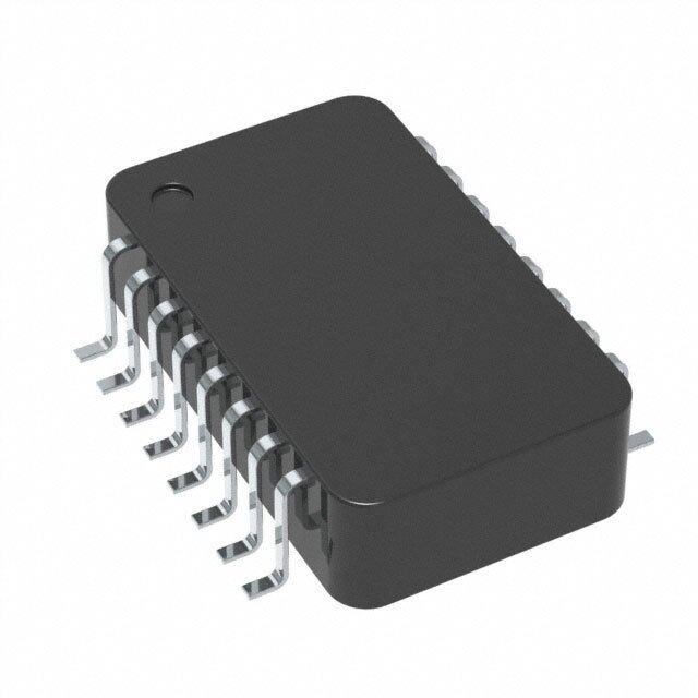
| 描述 | IC TXRX USB ESD-PROT 14TSSOPUSB 接口集成电路 USB Transceiver |
| 产品分类 | |
| 品牌 | Maxim Integrated |
| 产品手册 | |
| 产品图片 |
|
| rohs | 符合RoHS无铅 / 符合限制有害物质指令(RoHS)规范要求 |
| 产品系列 | 接口 IC,USB 接口集成电路,Maxim Integrated MAX3454EEUD+- |
| 数据手册 | |
| 产品型号 | MAX3454EEUD+ |
| 产品培训模块 | http://www.digikey.cn/PTM/IndividualPTM.page?site=cn&lang=zhs&ptm=25703http://www.digikey.cn/PTM/IndividualPTM.page?site=cn&lang=zhs&ptm=25705 |
| 产品目录页面 | |
| 产品种类 | USB 接口集成电路 |
| 供应商器件封装 | 14-TSSOP |
| 包装 | 管件 |
| 协议 | USB 2.0 |
| 双工 | 半 |
| 商标 | Maxim Integrated |
| 安装类型 | 表面贴装 |
| 安装风格 | SMD/SMT |
| 封装 | Tube |
| 封装/外壳 | 14-TSSOP(0.173",4.40mm 宽) |
| 封装/箱体 | TSSOP-14 |
| 工作温度 | -40°C ~ 85°C |
| 工作电源电压 | 1.65 V to 3.6 V, 3 V to 5.5 V |
| 工作电源电流 | 10 mA, 2.5 mA |
| 工厂包装数量 | 96 |
| 接口类型 | Differential Data Interface, Single End |
| 接收器滞后 | 250mV |
| 数据速率 | 12 Mbps, 480 Mbps |
| 最大工作温度 | + 85 C |
| 最小工作温度 | - 40 C |
| 标准 | USB 1.1 |
| 标准包装 | 96 |
| 电压-电源 | 1.65 V ~ 3.6 V |
| 类型 | Transceiver |
| 系列 | MAX3454E |
| 速度 | Full-Speed |
| 零件号别名 | MAX3454E |
| 驱动器/接收器数 | 1/1 |


PDF Datasheet 数据手册内容提取
19-2924; Rev 4; 2/06 ±15kV ESD-Protected USB Transceivers General Description Features M The MAX3453E–MAX3456E ±15kV ESD-protected USB- (cid:2) ±15kV ESD Protection on D+ and D- A compliant transceivers interface low-voltage ASICs with USB devices. The devices fully comply with USB 1.1 (cid:2) USB 1.1 and USB 2.0 (Low-Speed and Full-Speed)- X and USB 2.0 when operating at full (12Mbps) and low Compliant Transceivers 3 (1.5Mbps) speeds. The MAX3453E–MAX3456E operate (cid:2) Combined VP and VM Inputs/Outputs 4 wloiwth- vVoLltaagse lAowSI Cass. +1.65V, ensuring compatibility with (cid:2) +1.65V to +3.6V VLLogic Supply Input for 5 3 Interfacing with Low-Voltage ASICs The MAX3453E–MAX3456E feature a logic-selectable E suspend mode that reduces current consumption to (cid:2) Enumerate Input Function (MAX3453E/MAX3454E) less than 40µA. Integrated ±15kV ESD protection pro- – (cid:2) Powered from Li+ Battery as Low as +3.1V M tects the USB D+ and D- bidirectional bus connections. (MAX3454E/MAX3456E) The MAX3453E supports only full-speed (12Mbps) A operation. The MAX3453E/MAX3454E feature an inter- (cid:2) VBUSDetection (MAX3453E/MAX3455E) X nal 1.5kΩUSB pullup resistor and an enumeration func- (cid:2) Internal Pullup Resistor (MAX3453E/MAX3454E) tion that allows devices to logically disconnect while 3 plugged in. The MAX3453E/MAX3455E provide a push- (cid:2) No Power-Supply Sequencing Required 4 pull bus-detect (BD) output that asserts high when 5 VBUS> +4.0V. 6 The MAX3453E–MAX3456E operate over the extended E Ordering Information temperature range (-40°C to +85°C) and are available in 14-pin TSSOP and 16-pin (3mm x 3mm) thin QFN packages. PART TEMP RANGE PIN-PKG PKG CODE MAX3453EEUD -40oC to +85oC 14 TSSOP U14-1 Applications MAX3453EETE -40oC to +85oC 16 Thin QFN T1633-4 MAX3454EEUD -40oC to +85oC 14 TSSOP U14-1 PDAs MAX3454EETE -40oC to +85oC 16 Thin QFN T1633-4 PC Peripherals MAX3455EEUD -40oC to +85oC 14 TSSOP U14-1 Cellular Telephones MAX3455EETE -40oC to +85oC 16 Thin QFN T1633-4 Data Cradles MAX3456EEUD -40oC to +85oC 14 TSSOP U14-1 MP3 Players MAX3456EETE -40oC to +85oC 16 Thin QFN T1633-4 Selector Guide VBUS POWER- VL POWER- INTERNAL VBUS LEVEL USB SPEED ±15kV ESD PART SUPPLY SUPPLY PULLUP ENUMERATE DETECT SUPPORTED PROTECTION VOLTAGE (V) VOLTAGE (V) RESISTOR MAX3453E 4.0 to 5.5 1.65 to 3.6 Yes Yes Yes Full Yes MAX3454E 3.0 to 5.5 1.65 to 3.6 Yes No Yes Low/full Yes MAX3455E 4.0 to 5.5 1.65 to 3.6 No Yes No Low/full Yes MAX3456E 3.0 to 5.5 1.65 to 3.6 No No No Low/full Yes Typical Operating Circuit appears at end of data sheet. Pin Configurations appear at end of data sheet. ________________________________________________________________Maxim Integrated Products 1 For pricing, delivery, and ordering information,please contact Maxim/Dallas Direct!at 1-888-629-4642, or visit Maxim’s website at www.maxim-ic.com.
±15kV ESD-Protected USB Transceivers E ABSOLUTE MAXIMUM RATINGS 6 VBUS, VL, D+, D- to GND.......................................-0.3V to +6.0V Continuous Power Dissipation (TA= +70°C) 5 VTRMto GND............................................-0.3V to (VBUS+ 0.3V) 14-Pin TSSOP (derate 9.1mW/°C above +70°C).........727mW VP, VM, SUS, ENUM, SPD, 16-Pin Thin QFN (derate 14.7mW/°C above +70°C)....1176mW 4 RCV, OE, BD to GND................................-0.3V to (VL+ 0.3V) Operating Temperature Range...........................-40°C to +85°C 3 Current (into any pin)........................................................±15mA Junction Temperature......................................................+150°C Short-Circuit Current (D+ and D-)...................................±150mA Storage Temperature Range.............................-65°C to +150°C X Lead Temperature (soldering, 10s).................................+300°C A Stresses beyond those listed under “Absolute Maximum Ratings” may cause permanent damage to the device. These are stress ratings only, and functional M operation of the device at these or any other conditions beyond those indicated in the operational sections of the specifications is not implied. Exposure to absolute maximum rating conditions for extended periods may affect device reliability. – E 3 5 DC ELECTRICAL CHARACTERISTICS 4 (VBUS= +4.0V to +5.5V or VTRM= +3.0V to +3.6V, VL= +1.65V to +3.6V, TA= TMINto TMAX, unless otherwise noted. Typical values 3 are at VBUS= +5.0V, VL= +2.5V, and TA= +25°C.) (Note 1) X PARAMETER SYMB O L CONDITIONS MIN TYP MAX UNITS A SUPPLY INPUTS (VBUS, VTRM, VL) M Regulated Supply Voltage Output VTRM Internal regulator 3.0 3.3 3.6 V Full-speed transmitting and receiving at Operating Supply Current IVBUS 10 mA 12Mbps, CL = 50pF on D+ and D- (Note 2) Full-speed transmitting and receiving at Operating VL Supply Current IVL 2.5 mA 12Mbps (Note 2) Full-Speed Idle and SE0 Supply Full-speed idle: VD+ > 2.7V, VD- < 0.3V 250 350 IVBUS(IDLE) µA Current SE0: VD+ < 0.3V, VD- < 0.3V 250 350 Full-speed idle, MAX3453E/MAX3455E 15 Static VL Supply Current IVL(STATIC) SE0, or suspend µA mode MAX3454E/MAX3456E 5 MAX3453E (ENUM = low), 40 MAX3455E VM = VP = open, Suspend Supply Current IVBUS(SUSP) µA SUS = OE = high MAX3454E (ENUM = low), 35 MAX3456E Disable Mode Supply Current IVBUS(DIS) VL = GND or open 20 µA VBUS = GND or MAX3453E/MAX3455E 20 open, OE = low, Sharing Mode VL Supply Current IVL(SHARING) VP = low or high, µA VM = low or MAX3454E/MAX3456E 5 high, SUS = high D+/D- Sharing Mode Load ID_(SHARING) VBUS = GND or open, VD_ = 0 or +5.5V 20 µA Current D+/D- Disable Mode Load ID_(DIS) VL = GND or open, VD_ = 0 or +5.5V 5 µA Current 2 _______________________________________________________________________________________
±15kV ESD-Protected USB Transceivers DC ELECTRICAL CHARACTERISTICS (continued) M (VBUS= +4.0V to +5.5V or VTRM= +3.0V to +3.6V, VL= +1.65V to +3.6V, TA= TMINto TMAX, unless otherwise noted. Typical values A are at VBUS= +5.0V, VL= +2.5V, and TA= +25°C.) (Note 1) X PARAMETER SYMB O L CONDITIONS MIN TYP MAX UNITS 3 MAX3453E/MAX3455E, supply lost 3.6 4 MAX3453E/MAX3455E, supply present 4.0 5 USB Power-Supply Detection Threshold VTH_VBUS MAX3454E/MAX3456E, supply lost 0.8 V 3 MAX3454E/MAX3456E, supply present E 3.6 (Note 3) – USB Power-Supply Detection MAX3453E/MAX3455E 40 M VHYST_VBUS mV Hysteresis MAX3454E/MAX3456E 75 A VL Power-Supply Detection VTH_VL 0.85 V X Threshold 3 DIGITAL INPUTS/OUTPUTS (VP, VM, RCV, SUS, OE, SPD, BD, ENUM) 4 Input-Voltage Low VIL VM, VP, SUS, SPD, ENUM, OE 0.3 x VL V 5 Input-Voltage High VIH VM, VP, SUS, SPD, ENUM, OE 0.7 x VL V 6 Output-Voltage Low VOL VM, VP, RCV, BD, IOL = +2mA 0.4 V E Output-Voltage High VOH VM, VP, RCV, BD, IOH = -2mA VL - 0.4 V Input Leakage Current ILKG -1 +1 µA Input Capacitance CIN Measured from input to GND 10 pF ANALOG INPUTS/OUTPUTS (D+, D-) Differential Input Sensitivity VID |VD+ - VD-| 0.2 V Differential Common-Mode VCM Includes VID range 0.8 2.5 V Voltage Single-Ended Input Low Voltage VILSE 0.8 V Single-Ended Input High Voltage VIHSE 2.0 V Hysteresis VHYST 250 mV Output-Voltage Low VOLD RL = 1.5kΩ to +3.6V 0.3 V Output-Voltage High VOHD RL = 15kΩ to GND 2.8 3.6 V Off-State Leakage Current ILZ -1 +1 µA Transceiver Capacitance CIND Measured from D_ to GND 20 pF Driver Output Impedance ZDRV Steady-state drive 3.5 15.5 Ω Input Impedance ZIN Driver off 10 MΩ Internal Pullup Resistance RPULLUP ILOAD = 500µA (MAX3453E/MAX3454E) 1.425 1.575 kΩ (Note 4) ESD PROTECTION (D+, D-) Human Body Model ±15 kV IEC 61000-4-2 Contact Discharge ±8 kV _______________________________________________________________________________________ 3
±15kV ESD-Protected USB Transceivers E TIMING CHARACTERISTICS 6 (VBUS= +4.0V to +5.5V or VTRM = +3.0V to +3.6V, VL= +1.65V to +3.6V, TA= TMINto TMAX, unless otherwise noted. Typical values 5 are at VBUS= +5V, VL= +2.5V, and TA= +25°C.) (Note 1) 4 PARAMETER SYMBOL CONDITIONS MIN TYP MAX UNITS 3 DRIVER CHARACTERISTICS (Full-Speed Mode, CL = 50pF) X Rise Time tFR 10% to 90% of |VOHD - VOLD|, Figures 1, 6 4 20 ns A Fall Time tFF 90% to 10% of |VOHD - VOLD|, Figures 1, 6 4 20 ns M Excluding the first transition from idle state, Rise/Fall-Time Matching (Note 2) tFR / tFF 90 110 % Figures 1, 6 – E Output-Signal Crossover Voltage Excluding the first transition from idle state, VCRS_F 1.3 2.0 V 3 (Note 2) Figures 2, 6 5 tPLH_DRV Low-to-high transition, Figures 2, 6 18 Driver Propagation Delay ns 4 tPHL_DRV High-to-low transition, Figures 2, 6 18 3 tPHZ_DRV High-to-off transition, Figure 3 20 ns Driver Disable Delay X tPLZ_DRV Low-to-off transition, Figure 3 20 ns A tPZH_DRV Off-to-high transition, Figure 3 20 ns Driver Enable Delay M tPZL_DRV Off-to-low transition, Figure 3 20 ns DRIVER CHARACTERISTICS (low-speed mode, CL = 200pF to 600pF, MAX3454E/MAX3455E/MAX3456E) Rise Time tLR 10% to 90% of |VOHD - VOLD|, Figures 1, 6 75 300 ns Fall Time tLF 90% to 10% of |VOHD - VOLD|, Figures 1, 6 75 300 ns Excluding the first transition from idle state, Rise/Fall-Time Matching tLR / tLF 80 125 % Figures 1, 6 Excluding the first transition from idle state, Output-Signal Crossover Voltage VCRS_L 1.3 2.0 V Figures 2, 6 RECEIVER CHARACTERISTICS (CL = 15pF) Differential Receiver Propagation tPLH_RCV Low-to-high transition, Figures 4, 6 22 ns Delay tPHL_RCV High-to-low transition, Figures 4, 6 22 Single-Ended Receiver tPLH_SE Low-to-high transition, Figures 4, 6 12 ns Propagation Delay tPHL_SE High-to-low transition, Figures 4, 6 12 Single-Ended Receiver Disable tPHZ_SE High-to-off transition, Figure 5 15 ns Delay tPLZ_SE Low-to-off transition, Figure 5 15 Single-Ended Receiver Enable tPZH_SE Off-to-high transition, Figure 5 15 ns Delay tPZL_SE Off-to-low transition, Figure 5 15 Note 1: Parameters are 100% production tested at +25°C, unless otherwise noted. Limits over temperature are guaranteed by design. Note 2: Guaranteed by design, not production tested. Note 3: Production tested to +2.7V for VL< +3.0V. Note 4: Including external 27Ωseries resistor. 4 _______________________________________________________________________________________
±15kV ESD-Protected USB Transceivers Typical Operating Characteristics M (VBUS= +5.0V, VL= +3.3V, TA= +25°C, unless otherwise noted.) A X SINGLE-ENDED RECEIVER RISE-/FALL-TIME MATCHING RISE-/FALL-TIME MATCHING 3 PROPAGATION DELAY vs. VL (FULL SPEED) (LOW SPEED) 8 MAX3453E-56E toc02 MAX3453E-56E toc03 4 Y (ns) 67 CL = 15TpAF = +25°CTA = +85°C MAX3453E-56E toc01 CL = 50pF CL = 400pF 53E ELA 5 D+/D- D+/D- – ON D 4 1V/div 1V/div M AGATI 3 TA = -40°C A P O PR 2 X 1 3 4 0 1.6 1.8 2.0 2.2 2.4 2.6 2.8 3.0 3.2 3.4 3.6 20ns/div 100ns/div 5 VL (V) 6 E SUPPLY CURRENT LOGIC SUPPLY CURRENT OE, VP, VM TIMING vs. D+/D- CAPACITANCE vs. D+/D- CAPACITANCE CL = 15pF MAX3453E-56E toc04V2VP/div ENT (mA) 111222468024 MAX3453E-56E toc05 µURRENT (A) 334450505000000 SPD = VL, fIN = 6MHz MAX3453E-56E toc06 R C V2VM/div LY CUR 1102 UPPLY 220500 SUPP 8 SPD = VL, fIN = 6MHz GIC S 150 6 O OE L 100 4 5V/div 50 2 SPD = GND, fIN = 750kHz SPD = GND, fIN = 750kHz 0 0 20ns/div 0 50 100 150 200 250 300 350 400 0 50 100 150 200 250 300 350 400 D+/D- CAPACITANCE (pF) D+/D- CAPACITANCE (pF) _______________________________________________________________________________________ 5
±15kV ESD-Protected USB Transceivers E Pin Description 6 PIN 5 4 MAX3454E/ MAX3455E/ MAX3453E 3 NAME FUNCTION MAX3456E X A TSSOP THIN QFN TSSOP THIN QFN M Digital I/O Connections Logic Supply. Connect a +1.65V to – 1 15 1 15 VL +3.6V supply to VL. Bypass VL to GND with a 0.1µF ceramic E capacitor. 3 Speed Selector Input. Connect SPD to GND to select the low- 5 speed data rate (1.5Mbps). Connect SPD to VL to select the full- 4 2 1 — — SPD speed data rate (12Mbps). The MAX3453E only supports full- 3 speed operation. X Di ffere nti al Receiv er O utp ut. RCV re spo nds to the di ffere nti al in p uts 3 2 3 2 RCV A on D+ and D- (s ee Tabl e s 3, 4). RC V assert s lo w if SU S = V L. M Receiver Output/Driver Input. VP functions as a receiver output 4 3 4 3 VP when OE = VL. VP duplicates D+ when receiving. VP functions as a driver input when OE = GND. Receiver Output/Driver Input. VM functions as a receiver output 5 4 5 4 VM when OE = VL. VM duplicates D- when receiving. VM functions as a driver input when OE = GND. No Connection. Not internally connected. 6, 13* 5, 8, 13*, 16 6 5, 8, 16 N.C. *Pin 13 is No Connection for MAX3456E only. 7 6 7 6 GND Ground Suspend Input. Drive SUS low for normal operation. Drive SUS high to put the MAX3453E–MAX3456E into suspend mode. RCV 8 7 8 7 SUS asserts low in suspend mode. VP and VM remain active in suspend mode. Output Enable. Drive OE to GND to enable the transmitter 9 9 9 9 OE outputs. Drive OE to VL to disable the transmitter outputs. OE also controls the I/O direction of VP and VM (see Tables 3, 4). USB Input/Output. For OE = GND, D- functions as a USB output, with VM providing the input signal. For OE = VL, D- functions as a USB input, with VM functioning as a single-ended 10 10 10 10 D- receiver output. Connect a 1.5kΩ resistor from D- to VTRM for low-speed (1.5Mbps) operation (MAX3455E/MAX3456E). Drive ENUM to VL to connect the internal 1.5kΩ resistor from D- to VTRM for low-speed (MAX3454E, SPD = GND) operation. 6 _______________________________________________________________________________________
±15kV ESD-Protected USB Transceivers Pin Description (continued) M PIN A X MAX3454E/ MAX3455E/ MAX3453E 3 NAME FUNCTION MAX3456E 4 5 TSSOP THIN QFN TSSOP THIN QFN 3 E USB Input/Output. For OE = GND, D+ functions as a USB output, with VP providing the input signal. For OE = VL, D+ – functions as a USB input, with VP functioning as a single-ended M receiver output. Connect a 1.5kΩ resistor from D+ to VTRM for 11 11 11 11 D+ A full-speed (12Mbps) operation (MAX3455E/MAX3456E). Drive ENUM to VL to connect the internal 1.5kΩ resistor (MAX3453E/ X MAX3454E) from D+ to VTRM for full-speed (MAX3454E, SPD = 3 VL) operation. 4 Internal Regulator Output. VTRM provides a regulated +3.3V 5 output. Bypass VTRM to GND with a 1µF (min) ceramic 6 capacitor as close to the device as possible. VTRM normally E derives power from VBUS. Alternatively, drive VTRM directly with 12 12 12 12 VTRM a +3.3V ±10% supply (MAX3454E/MAX3456E). VTRM provides power to internal circuitry and provides the pullup voltage for an external USB pullup resistor (MAX3455E/MAX3456E). Do not use VTRM to power external circuitry. 13 13 Bus-Detection Output (MAX3453E/MAX3455E). The push-pull (MAX3455E (MAX3455E 13 13 BD BD output asserts low and the device enters sharing mode if only) only) VBUS < +3.6V. BD asserts high if VBUS > +4.0V. Enumerate Function Selection Input (MAX3453E/MAX3454E). Drive ENUM to VL to connect the internal 1.5kΩ resistor 13 13 between VTRM and D+ or D-, depending on the state of SPD. (MAX3454E (MAX3454E 2 1 ENUM Drive ENUM to GND to disconnect the internal 1.5kΩ resistor. only) only) For SPD = VL, the 1.5kΩ resistor connects to D+. For SPD = GND, the 1.5kΩ resistor connects to D-. For the MAX3453E, the resistor only connects to D+. USB Power-Supply Input. Connect a +4.0V to +5.5V power supply to VBUS. VBUS provides power to the internal linear regulator. Bypass VBUS to GND with a 0.1µF ceramic capacitor 14 14 14 14 VBUS as close to the device as possible. Connect VBUS and VTRM together when powering the MAX3454E/MAX3456E with an external power supply (+3.3V ±10%). _______________________________________________________________________________________ 7
±15kV ESD-Protected USB Transceivers E Functional Diagram 6 5 4 3 X A MAX3453E TO INTERNAL M CIRCUITRY BD – LDO VBUS E VTH_VBUS REGULATOR 3 5 VL VTRM 4 3 X VP D+ A D- M VM OE LEVEL TRANSLATOR RCV SUS TO INTERNAL CIRCUITRY 1.5kΩ VTRM ENUM GND 8 _______________________________________________________________________________________
±15kV ESD-Protected USB Transceivers Functional Diagram (continued) M A X 3 4 MAX3454E– 5 MAX3456E 3 TO INTERNAL MAX3455E ONLY CIRCUITRY E BD LDO VBUS – VTH_VBUS REGULATOR M A VL VTRM X SPD 3 4 VP 5 D+ 6 D- VM E OE LEVEL TRANSLATOR RCV SUS TO INTERNAL CIRCUITRY MAX3454E ONLY 1.5kΩ VTRM SPD CONTROL ENUM LOGIC GND _______________________________________________________________________________________ 9
±15kV ESD-Protected USB Transceivers E Detailed Description pullup resistor, allowing the MAX3453E/MAX3454E to simulate a bus disconnect while powered and connect- 6 The MAX3453E–MAX3456E USB-compliant transceivers ed to the USB cable. The MAX3453E/MAX3455E fea- 5 cUoSnBv esritg snianlgs,le a-enndd UedS Bo rs idginffaelrse ntoti asl inloggleic-e-lenvdeeld s iogrn dailfsfe tro- ture a bus-detect output (BD) that asserts high if VBUS 4 ential logic-level signals. The MAX3453E fully complies > +4V. BD asserts low if VBUS < +3.6V. The 3 MAX3455E/MAX3456E require external pullup resistors with full-speed (12Mbps) operation under USB specifica- X tion 2.0. The MAX3454E–MAX3456E fully comply with from either D+ or D- to VTRM to utilize the appropriate bus speed. The MAX3456E is pin-for-pin compatible USB specification 1.1, and full-speed (12Mbps) and low- A with the Micrel MIC2550A. speed (1.5Mbps) operation under USB specification 2.0. M The MAX3453E–MAX3456E operate with VL as low as Applications Information +1.65V, ensuring compatibility with low-voltage ASICs. – Power-Supply Configurations E The MAX3453E–MAX3456E derive power from the USB Normal Operating Mode 3 h(MoAstX 3(4V5B4UES/M) AoXr3 4f5r6oEm) cao nsniencgteled- ctoe lVl BLUiS+o rb farottme ray Connect VLand VBUSto system power supplies (Table 1). 5 +3.3V regulated supply connected to VBUS and VTRM. Connect VL to a +1.65V to +3.6V supply. Connect VBUS 4 The MAX3453E–MAX3456E meet the physical layer to a +4.0V to +5.5V supply. Alternatively, the MAX3454E/ MAX3456E can derive power from a single Li+ battery. 3 specifications for logic-level supply voltages (VL) from X +1.65V to +3.6V. Integrated ±15kV ESD protection safe- Connect the battery to VBUS. guards the D+ and D- USB I/O ports. Additionally, the MAX3454E/MAX3456E can derive A power from a +3.3V ±10% voltage regulator. Connect The MAX3453E/MAX3454E feature an enumerate func- M tion providing an internal 1.5kΩ pullup resistor from D+ VBUS and VTRM to an external +3.3V voltage regulator. (MAX3453E/MAX3454E) or D- (MAX3454E only) to VBUS no longer consumes current to power the internal VTRM. The enumerate function disconnects the 1.5kΩ linear regulator in this configuration. Table 1. Power-Supply Configurations VBUS (V) VTRM (V) VL (V) CONFIGURATION NOTES 4.0 to 5.5 3.0 to 3.6 output 1.65 to 3.6 Normal mode — 3.1 to 4.5 3.0 to 3.6 output 1.65 to 3.6 Battery supply MAX3454E/MAX3456E 3.0 to 3.6 3.0 to 3.6 input 1.65 to 3.6 Voltage regulator supply MAX3454E/MAX3456E GND or floating High-Z 1.65 to 3.6 Sharing mode Table 2 3.0 to 5.5 High-Z GND or floating Disable mode Table 2 Table 2. Disable-Mode and Sharing-Mode Connections INPUTS/OUTPUTS DISABLE MODE SHARING MODE • Floating or connected to GND VBUS/VTRM +3.0V to +5.5V / High Impedance (MAX3453E/MAX3454E/MAX3456E) / High Impedance • < 3.6V (MAX3453E/MAX3455E) / High Impedance VL Floating or connected to GND 1.65V to 3.6V input D+ and D- High impedance High impedance High impedance for OE = low VP and VM Invalid* High for OE = high RCV Invalid* Undefined** SPD (MAX3454E–MAX3456E), SUS, OE, ENUM High impedance High impedance (MAX3453E/MAX3454E) BD (MAX3453E/MAX3455E) Invalid* Low *High impedance or low. **High or low. 10 ______________________________________________________________________________________
±15kV ESD-Protected USB Transceivers Disable Mode Table 3a. Transmit Truth Table M Connect VBUS to a system power supply and leave VL (OE = 0, SUS = 0) unconnected or connect to GND. D+ and D- enter a tri- A state mode and VBUS (or VBUS and VTRM) consumes INPUTS OUTPUTS X less than 20µA of supply current. D+ and D- withstand OUTPUT STATE VP VM D+ D- RCV 3 external signals up to +5.5V in disable mode (Table 2). 0 0 0 0 X SE0 4 Sharing Mode 0 1 0 1 0 Logic 0 5 Connect VL to a system power supply and leave VBUS 1 0 1 0 1 Logic 1 3 (or VBUS and VTRM) unconnected or connect to GND. D+ and D- enter a tri-state mode, allowing other circuitry 1 1 1 1 X Undefined E to share the USB D+ and D- lines, and VLconsumes less X= Undefined. – than 20µA of supply current. D+ and D- withstand M external signals up to +5.5V in sharing mode (Table 2). A Table 3b. Transmit Truth Table Device Control X (OE = 0, SUS = 1) OE 3 OE controls the direction of communication. Drive OE INPUTS OUTPUTS 4 low to transfer data from the logic side to the USB side. OUTPUT STATE For OE = low, VP and VM serve as differential driver VP VM D+ D- RCV 5 inputs to the USB transmitter. 0 0 0 0 0 SE0 6 E Drive OE high to transfer data from the USB side to the 0 1 0 1 0 Logic 0 logic side. For OE = high, VP and VM serve as single- 1 0 1 0 0 Logic 1 ended receiver outputs from the USB inputs 1 1 1 1 0 Undefined (D+ and D-). RCV serves as a differential receiver out- put, regardless of the state of OE. ENUM (MAX3453E/MAX3454E) Table 4a. Receive Truth Table The MAX3453E/MAX3454E feature an enumerate func- tion that allows software control of USB enumeration. (OE = 1 and SUS = 0) USB protocol requires a 1.5kΩ pullup resistor to D+ or D- to indicate the transmission speed to the host (see INPUTS OUTPUTS OUTPUT STATE the SPD section). The MAX3453E/MAX3454E provide D+ D- VP VM RCV an internal 1.5kΩ pullup resistor. Disconnect the pullup 0 0 0 0 X SE0 resistor from the circuit to simulate the removal of a 0 1 0 1 0 Logic 0 device from the USB. Drive ENUM low to disconnect the internal pullup resistor. Drive ENUM high to connect 1 0 1 0 1 Logic 1 the internal pullup resistor. The SPD state (MAX3454E 1 1 1 1 X Undefined only) determines whether the pullup resistor connects X= Undefined. to D+ or D-. For ENUM = high, the internal pullup resis- tor connects to D+ when SPD = VL (full speed) or to D- when SPD = GND (low speed). The MAX3453E only Table 4b. Receive Truth Table supports full-speed operation; therefore, the pullup resistor only connects to D+ or is disconnected. (OE = 1 and SUS = 1) tFR, tLR tFF, tLF INPUTS OUTPUTS OUTPUT STATE VOHD D+ D- VP VM RCV 90% 90% 0 0 0 0 0 SE0 0 1 0 1 0 Logic 0 1 0 1 0 0 Logic 1 10% 10% 1 1 1 1 0 Undefined VOLD Figure 1. Rise and Fall Times ______________________________________________________________________________________ 11
±15kV ESD-Protected USB Transceivers E SPD (MAX3454E/MAX3455E/MAX3456E) SPD sets the transceiver speed. Connect SPD to GND 6 to select the low-speed data rate (1.5Mbps). Connect VP AND VM RISE/FALL TIMES < 4ns 5 VM SPD to VL to select the full-speed data rate (12Mbps). 4 The MAX3454E provides an internal pullup resistor for 3 selecting the bus speed. The MAX3455E and X MAX3456E require an external pullup resistor to D+ or VP D- to set the bus speed. Connect the 1.5kΩ resistor A between D+ and VTRM to set the full-speed (12Mbps) tPLH_DRV tPHL_DRV M data rate, or connect the 1.5kΩresistor between D- and VTRMto set the low-speed (1.5Mbps) data rate. – D- E SUS 3 The SUS state determines whether the MAX3453E– VCRS_F , VCRS_L MAX3456E operate in normal mode or in suspend 5 mode. Connect SUS to GND to enable normal opera- D+ 4 tion. Drive SUS high to enable suspend mode. RCV 3 asserts low and VP and VM remain active in suspend X mode (Tables 3 and 4). Supply current decreases in Figure 2. Timing of VP and VM to D+ and D- A suspend mode (see the Electrical Characteristics). BD (MAX3453E/MAX3455E) M External Components The push-pull bus detect (BD) output monitors VBUS and asserts high if VBUS is greater than +4.0V. BD External Resistors asserts low if VBUS is less than +3.6V and the Proper USB operation requires two external resistors, MAX3453E/MAX3455E enters sharing mode (Table 2). each 27Ω ±1%, 1/8W (or greater). Install one resistor in series between D+ of the MAX3453E–MAX3456E and VTRM D+ on the USB connector. Install the other resistor in An internal linear regulator generates the VTRM voltage series between D- of the MAX3453E–MAX3456E and D- (+3.3V, typ). VTRM derives power from VBUS (see the on the USB connector (see Typical Operating Circuit). Power-Supply Configurations section). VTRM powers the The MAX3455E/MAX3456E require an external 1.5kΩ internal portions of the USB circuitry and provides the pullup voltage for an external USB pullup resistor pullup resistor between VTRM and D+ or D- to set the bus speed. (MAX3455E/MAX3456E). Bypass VTRM to GND with a 1µF ceramic capacitor as close to the device as possible. External Capacitors Do not use VTRMto provide power to external circuitry. The MAX3453E–MAX3456E require three external D+ and D- capacitors for proper operation. Bypass VLto GND with a D+ and D- serve as bidirectional bus connections and 0.1µF ceramic capacitor. Bypass VBUS to GND with a are ESD protected to ±15kV (Human Body Model). For 0.1µF ceramic capacitor. Bypass VTRM to GND with a 1µF (min) ceramic capacitor. Install all capacitors as OE = low, D+ and D- serve as transmitter outputs. For close to the device as possible. OE= high, D+ and D- serve as receiver inputs. Data Transfer VBUS For most applications, VBUS connects to the VBUS termi- Transmitting Data to the USB nal on the USB connector (see the Power-Supply The MAX3453E–MAX3456E transmit data to the USB Configurations section). VBUS can also connect to an differentially on D+ and D-. VP and VM serve as differ- external supply as low as +3.1V (MAX3454E/MAX3456E). ential input signals to the driver (Tables 3a and 3b). Drive VBUSlow to enable sharing mode. Bypass VBUSto Receiving Data from the USB GND with a 0.1µF ceramic capacitor as close to the To receive data from the USB, drive OE high and SUS device as possible. low. Differential data received by D+ and D- appears as a differential logic signal at RCV. Single-ended receivers on D+ and D- drive VP and VM, respectively (Tables 4a and 4b). 12 ______________________________________________________________________________________
±15kV ESD-Protected USB Transceivers M A OE OE X 3 VP/VM CONNECTED TO GND, D+/D- CONNECTED TO GND, 4 D+/D- CONNECTED TO PULLUP VP/VM CONNECTED TO PULLUP 5 D+/D- VP/VM 3 E tPLZ_DRV tPZL_DRV tPLZ_SE tPZL_SE – M VP/VM CONNECTED TO VL, D+/D- CONNECTED TO +3V, A OE D+/D- CONNECTED TO PULLDOWN OE VP/VM CONNECTED TO PULLDOWN X 3 VP/VM 4 D+/D- 5 6 tPHZ_DRV tPZH_DRV tPHZ_SE tPZH_SE E Figure 3. Enable and Disable Timing, Driver Figure 5. Enable and Disable Timing, Receiver INPUT RISE/FALL TIME < 4ns +3V MAX3453E– TEST D+/D- MAX3456E POINT RCV, VM, 0V AND VP CL (a) LOAD FOR RCV, VM, AND VP TEST MAX3453E– tPLVHL_RCV, MAX3456E 27Ω POINT tPLH_SE D+ AND D- CL tPHL_RCV, (b) LOAD FOR D+/D- 15kΩ RCV, VM, AND VP tPHL_SE Figure 4. Timing of D+ and D- to RCV, VM, and VP Figure 6. Test Circuits ______________________________________________________________________________________ 13
±15kV ESD-Protected USB Transceivers E ESD Protection RC RD 6 D+ and D- possess extra protection against static elec- 1MΩ 1.5kΩ 5 tricity to protect the devices up to ±15kV. The ESD structures withstand high ESD in all operating modes: CHARGE-CURRENT- DISCHARGE 4 LIMIT RESISTOR RESISTANCE normal operation, suspend mode, and powered down. 3 AX D•+± 1a5nkdV D u-s pinrgo vthidee H puromteacnt iBoond tyo Mthoed feolllowing limits: VOHLDIGTCAHG-E 100CpFs SCTAOPRAACGITEOR DUTENEVDSICETRE • ±8kV using the Contact Discharge method specified SOURCE M in IEC 61000-4-2 – ESD Test Conditions E ESD performance depends on a variety of conditions. 3 Contact Maxim for a reliability report that documents Figure 7. Human Body ESD Test Models 5 test setup, test methodology, and test results. 4 Human Body Model 3 Figure 7 shows the Human Body Model and Figure 8 X shows the current waveform generated when dis- IP 100% Ir PEAK-TO-PEAK RINGING 90% (NOT DRAWN TO SCALE) charged into a low impedance. This model consists of A a 100pF capacitor charged to the ESD voltage of inter- M AMPERES est, which then discharges into the test device through a 1.5kΩresistor. 36.8% IEC 61000-4-2 10% The IEC 61000-4-2 standard covers ESD testing and 0 0 TIME performance of finished equipment. It does not specifi- tRL tDL cally refer to integrated circuits. The major difference CURRENT WAVEFORM between tests done using the Human Body Model and IEC 61000-4-2 is a higher peak current in IEC 61000-4- Figure 8. Human Body Model Current Waveform 2, due to lower series resistance. Hence, the ESD with- stand voltage measured to IEC 61000-4-2 generally is lower than that measured using the Human Body Model. Figure 9 shows the IEC 61000-4-2 model. The RC RD 50MΩ to 100MΩ 330Ω Contact Discharge method connects the probe to the device before the probe is charged. CHARGE-CURRENT- DISCHARGE LIMIT RESISTOR RESISTANCE Machine Model The Machine Model for ESD tests all connections using HIGH- DEVICE a 200pF storage capacitor and zero discharge resis- VOLTAGE Cs STORAGE UNDER DC 150pF CAPACITOR TEST tance. Its objective is to emulate the stress caused by SOURCE contact that occurs with handling and assembly during manufacturing. All pins require this protection during manufacturing, not just inputs and outputs. After PC board assembly, the Machine Model is less relevant to I/O ports. Figure 9. IEC 61000-4-2 ESD Test Model Chip Information TRANSISTOR COUNT: 873 PROCESS: BiCMOS 14 ______________________________________________________________________________________
±15kV ESD-Protected USB Transceivers Typical Operating Circuits M A +1.65V TO +3.6V X 0.1µF 0.1µF 3 PC 4 VL(I/O) BD* VL VBUS UPOSBWER 5 27Ω 1% 3 VP D+ D+ E 27Ω 1% – VM MAX3453E D- D- M ASIC MAX3454E RCV GND GND A USB CABLE X ENUM 15kΩ 15kΩ 3 SUS 4 5 SPD** VTRM 6 1µF OE E GND *MAX3453E ONLY. **MAX3454E ONLY. +1.65V TO +3.6V 0.1µF 0.1µF PC VL(I/O) VP VL VBUS USB POWER VM VTRM 1µF RCV MAX3455E 1.5kΩ*** ASIC MAX3456E* BD** 27Ω 1% D+ D+ SUS 27Ω 1% SPD D- D- OE GND GND GND USB CABLE 15kΩ 15kΩ *PIN COMPATIBLE WITH MICREL MIC2550A. **MAX3455E ONLY. ***CONNECT TO D+ FOR FULL-SPEED OPERATION. CONNECT TO D- FOR LOW-SPEED OPERATION. ______________________________________________________________________________________ 15
±15kV ESD-Protected USB Transceivers E Pin Configurations 6 5 TOP VIEW 4 3 VL 1 14 VBUS VL 1 14 VBUS X ENUM 2 13 BD SPD 2 13 N.C. (ENUM*) (BD**) A RCV 3 MAX3453E 12 VTRM RCV 3 MAX3454E 12 VTRM M MAX3455E VP 4 11 D+ VP 4 MAX3456E 11 D+ – E VM 5 10 D- VM 5 10 D- 3 N.C. 6 9 OE N.C. 6 9 OE 5 GND 7 8 SUS GND 7 8 SUS 4 3 TSSOP TSSOP X MA N.C. VL VBUS BD N.C. VL VBUS N.C.(ENUM*)(BD**) 16 15 14 13 16 15 14 13 ENUM 1 12 VTRM SPD 1 12 VTRM RCV 2 MAX3453E 11 D+ RCV 2 MAX3454E 11 D+ MAX3455E MAX3456E VP 3 10 D- VP 3 10 D- ***EXPOSED PADDLE ***EXPOSED PADDLE VM 4 9 OE VM 4 9 OE 5 6 7 8 5 6 7 8 N.C. GND SUS N.C. N.C. GND SUS N.C. 3mm x 3mm 3mm x 3mm THIN QFN THIN QFN *MAX3454E ONLY. **MAX3455E ONLY. ***CONNECT EXPOSED PADDLE TO GND OR LEAVE FLOATING. 16 ______________________________________________________________________________________
±15kV ESD-Protected USB Transceivers Package Information M (The package drawing(s) in this data sheet may not reflect the most current specifications. For the latest package outline information, A go to www.maxim-ic.com/packages.) X S 3 P MARKING E (NE - 1) X e N.E 4 HI 5 E/2 N T 3 (ND - 1) X e D2/2 QF E D/2 AAAA 6L – e 1 D CL D2 12x M A X k b 0.10 M C A B 3 CL L E2/2 4 5 E2 6 E CL CL 0.10 C 0.08 C A A2 A1 L L e e PACKAGE OUTLINE 8, 12, 16L THIN QFN, 3x3x0.8mm 1 21-0136 G 2 ______________________________________________________________________________________ 17
±15kV ESD-Protected USB Transceivers E Package Information (continued) 6 (The package drawing(s) in this data sheet may not reflect the most current specifications. For the latest package outline information, 5 go to www.maxim-ic.com/packages.) 4 3 X PKG 8L 3x3 12L 3x3 16L 3x3 EXPOSED PAD VARIATIONS A REF. MIN. NOM.MAX. MIN. NOM.MAX. MIN. NOM.MAX. PKG. D2 E2 DOWN M A 0.70 0.75 0.80 0.70 0.75 0.80 0.70 0.75 0.80 CODES MIN. NOM. MAX. MIN. NOM. MAX. PIN ID JEDEC ABLOLNODWSE D b 0.25 0.30 0.35 0.20 0.25 0.30 0.20 0.25 0.30 TQ833-1 0.25 0.70 1.25 0.25 0.70 1.25 0.35 x 45¡ WEEC NO – D 2.90 3.00 3.10 2.90 3.00 3.10 2.90 3.00 3.10 T1233-1 0.95 1.10 1.25 0.95 1.10 1.25 0.35 x 45¡ WEED-1 NO E E 2.90 3.00 3.10 2.90 3.00 3.10 2.90 3.00 3.10 T1233-3 0.95 1.10 1.25 0.95 1.10 1.25 0.35 x 45¡ WEED-1 YES e 0.65 BSC. 0.50 BSC. 0.50 BSC. T1233-4 0.95 1.10 1.25 0.95 1.10 1.25 0.35 x 45¡ WEED-1 YES 3 L 0.35 0.55 0.75 0.45 0.55 0.65 0.30 0.40 0.50 T1633-1 0.95 1.10 1.25 0.95 1.10 1.25 0.35 x 45¡ WEED-2 NO N 8 12 16 5 T1633-2 0.95 1.10 1.25 0.95 1.10 1.25 0.35 x 45¡ WEED-2 YES ND 2 3 4 4 NE 2 3 4 T1633F-3 0.65 0.80 0.95 0.65 0.80 0.95 0.225 x 45¡ WEED-2 N/A 3 A1 0 0.02 0.05 0 0.02 0.05 0 0.02 0.05 T1633FH-3 0.65 0.80 0.95 0.65 0.80 0.95 0.225 x 45¡ WEED-2 N/A A2 0.20 REF 0.20 REF 0.20 REF T1633-4 0.95 1.10 1.25 0.95 1.10 1.25 0.35 x 45¡ WEED-2 NO X k 0.25 - - 0.25 - - 0.25 - - A M NOTES: 1. DIMENSIONING & TOLERANCING CONFORM TO ASME Y14.5M-1994. 2. ALL DIMENSIONS ARE IN MILLIMETERS. ANGLES ARE IN DEGREES. 3. N IS THE TOTAL NUMBER OF TERMINALS. 4. THE TERMINAL #1 IDENTIFIER AND TERMINAL NUMBERING CONVENTION SHALL CONFORM TO JESD 95-1 SPP-012. DETAILS OF TERMINAL #1 IDENTIFIER ARE OPTIONAL, BUT MUST BE LOCATED WITHIN THE ZONE INDICATED. THE TERMINAL #1 IDENTIFIER MAY BE EITHER A MOLD OR MARKED FEATURE. 5. DIMENSION b APPLIES TO METALLIZED TERMINAL AND IS MEASURED BETWEEN 0.20 mm AND 0.25 mm FROM TERMINAL TIP. 6. ND AND NE REFER TO THE NUMBER OF TERMINALS ON EACH D AND E SIDE RESPECTIVELY. 7. DEPOPULATION IS POSSIBLE IN A SYMMETRICAL FASHION. 8. COPLANARITY APPLIES TO THE EXPOSED HEAT SINK SLUG AS WELL AS THE TERMINALS. 9. DRAWING CONFORMS TO JEDEC MO220 REVISION C. 10. MARKING IS FOR PACKAGE ORIENTATION REFERENCE ONLY. 11. NUMBER OF LEADS SHOWN ARE FOR REFERENCE ONLY. PACKAGE OUTLINE 8, 12, 16L THIN QFN, 3x3x0.8mm 2 21-0136 G 2 18 ______________________________________________________________________________________
±15kV ESD-Protected USB Transceivers Package Information (continued) M (The package drawing(s) in this data sheet may not reflect the most current specifications. For the latest package outline information, A go to www.maxim-ic.com/packages.) X 3 S P E 4 m. 0m 5 4 P4. 3 O SS E T – M A X 3 4 5 6 E PACKAGE OUTLINE, TSSOP 4.40mm BODY 1 21-0066 G 1 Revision History Pages changed at Rev1: 1, 14, 19, slide Maxim cannot assume responsibility for use of any circuitry other than circuitry entirely embodied in a Maxim product. No circuit patent licenses are implied. Maxim reserves the right to change the circuitry and specifications without notice at any time. Maxim Integrated Products, 120 San Gabriel Drive, Sunnyvale, CA 94086 408-737-7600 ____________________19 © 2006 Maxim Integrated Products is a registered trademark of Maxim Integrated Products.
Mouser Electronics Authorized Distributor Click to View Pricing, Inventory, Delivery & Lifecycle Information: M axim Integrated: MAX3453EETE+ MAX3454EETE+ MAX3454EEUD+ MAX3453EETE+T MAX3454EETE+T MAX3454EEUD+T MAX3456EETE+ MAX3456EETE+T