ICGOO在线商城 > 集成电路(IC) > 接口 - 驱动器,接收器,收发器 > DP83849IVS/NOPB

 Datasheet下载
- 型号: DP83849IVS/NOPB
- 制造商: Texas Instruments
- 库位|库存: xxxx|xxxx
- 要求:
| 数量阶梯 | 香港交货 | 国内含税 |
| +xxxx | $xxxx | ¥xxxx |
查看当月历史价格
查看今年历史价格
DP83849IVS/NOPB产品简介:
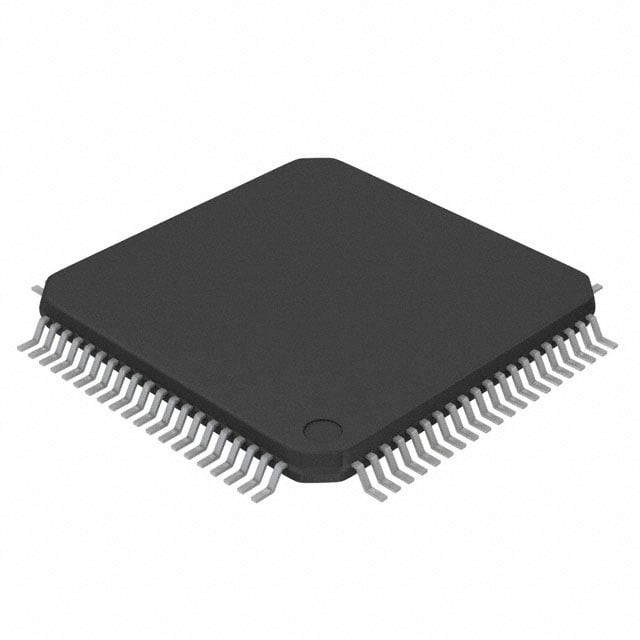
ICGOO电子元器件商城为您提供DP83849IVS/NOPB由Texas Instruments设计生产,在icgoo商城现货销售,并且可以通过原厂、代理商等渠道进行代购。 DP83849IVS/NOPB价格参考。Texas InstrumentsDP83849IVS/NOPB封装/规格:接口 - 驱动器,接收器,收发器, 收发器 2/2 以太网 80-TQFP(12x12)。您可以下载DP83849IVS/NOPB参考资料、Datasheet数据手册功能说明书,资料中有DP83849IVS/NOPB 详细功能的应用电路图电压和使用方法及教程。
Texas Instruments(德州仪器)的DP83849IVS/NOPB是一款用于接口应用的驱动器、接收器和收发器。它属于以太网物理层(PHY)收发器系列,支持10/100 Mbps以太网通信标准。以下是该型号的主要应用场景:

 1. 工业自动化与控制
   DP83849IVS/NOPB广泛应用于工业自动化领域,特别是在需要可靠网络连接的环境中。它可以用于连接PLC(可编程逻辑控制器)、HMI(人机界面)设备以及各种传感器和执行器。通过以太网接口,这些设备可以实现高速数据传输,确保工业控制系统中的实时性和稳定性。

 2. 楼宇自动化
   在智能建筑中,该芯片可以用于连接各种监控设备、安防系统、照明控制和环境控制系统。它能够提供稳定的数据传输,确保楼宇管理系统中的各个子系统能够高效协同工作。例如,通过以太网连接的温控器、门禁系统等设备可以通过DP83849IVS/NOPB进行数据交换。

 3. 汽车电子
   在现代汽车中,以太网逐渐成为车载网络的标准之一。DP83849IVS/NOPB可以用于汽车内部的通信系统,如车载娱乐系统、高级驾驶辅助系统(ADAS)和车辆诊断系统。它能够在复杂的电磁环境中保持稳定的通信性能,确保车辆内部各个模块之间的数据传输安全可靠。

 4. 通信基础设施
   该芯片也适用于小型网络设备,如路由器、交换机和无线接入点。它能够为这些设备提供高效的以太网接口,确保网络数据的快速传输和处理。在一些小型企业或家庭网络环境中,DP83849IVS/NOPB可以作为核心组件,帮助构建稳定可靠的局域网。

 5. 嵌入式系统
   对于需要以太网连接的嵌入式设备,DP83849IVS/NOPB是一个理想的选择。它可以集成到各种嵌入式系统中,如医疗设备、智能家居控制器等。通过以太网接口,这些设备可以与外部网络进行数据交互,实现远程监控和管理功能。

总的来说,DP83849IVS/NOPB凭借其高可靠性和低功耗特性,适合应用于对网络性能要求较高的场景,尤其是在工业、汽车和通信等领域。
| 参数 | 数值 |
| 产品目录 | 集成电路 (IC)半导体 |
| 描述 | IC TXRX ETHERNET PHY DUAL 80TQFP以太网 IC PHYTER DUAL COMM TEMP DUAL PORT |
| 产品分类 | |
| 品牌 | Texas Instruments |
| 产品手册 | |
| 产品图片 |
|
| rohs | 符合RoHS无铅 / 符合限制有害物质指令(RoHS)规范要求 |
| 产品系列 | 通信及网络 IC,以太网 IC,Texas Instruments DP83849IVS/NOPB- |
| 数据手册 | |
| 产品型号 | DP83849IVS/NOPB |
| 产品 | Ethernet Transceivers |
| 产品目录页面 | |
| 产品种类 | 以太网 IC |
| 以太网连接类型 | 10Base-T, 100Base-TX |
| 供应商器件封装 | 80-TQFP |
| 其它名称 | *DP83849IVS/NOPB |
| 包装 | 托盘 |
| 协议 | 以太网 |
| 双工 | - |
| 商标 | Texas Instruments |
| 安装类型 | 表面贴装 |
| 安装风格 | SMD/SMT |
| 封装 | Tray |
| 封装/外壳 | 80-TQFP |
| 封装/箱体 | TQFP-80 |
| 工作温度 | -40°C ~ 85°C |
| 工厂包装数量 | 119 |
| 接口 | MII, RMII, SNI |
| 接收器滞后 | - |
| 支持标准 | 802.3u, 802.3u ENDEC, 802.3u MII, 802.3u PCS, 1149.1 JTAG |
| 数据速率 | - |
| 最大功率耗散 | 600 mW |
| 最大工作温度 | + 85 C |
| 最小工作温度 | - 40 C |
| 标准包装 | 119 |
| 电压-电源 | 3 V ~ 3.6 V |
| 电源电压-最大 | 3.6 V |
| 电源电压-最小 | 3 V |
| 类型 | 收发器 |
| 系列 | DP83849I |
| 配用 | /product-detail/zh/DP83849IVS-EVK/DP83849IVS-EVK-ND/1640565 |
| 驱动器/接收器数 | 2/2 |


- 商务部:美国ITC正式对集成电路等产品启动337调查
- 曝三星4nm工艺存在良率问题 高通将骁龙8 Gen1或转产台积电
- 太阳诱电将投资9.5亿元在常州建新厂生产MLCC 预计2023年完工
- 英特尔发布欧洲新工厂建设计划 深化IDM 2.0 战略
- 台积电先进制程称霸业界 有大客户加持明年业绩稳了
- 达到5530亿美元!SIA预计今年全球半导体销售额将创下新高
- 英特尔拟将自动驾驶子公司Mobileye上市 估值或超500亿美元
- 三星加码芯片和SET,合并消费电子和移动部门,撤换高东真等 CEO
- 三星电子宣布重大人事变动 还合并消费电子和移动部门
- 海关总署:前11个月进口集成电路产品价值2.52万亿元 增长14.8%


PDF Datasheet 数据手册内容提取
Product Sample & Technical Tools & Support & Reference Folder Buy Documents Software Community Design DP83849I SNOSAX1F–MAY2008–REVISEDSEPTEMBER2015 DP83849I PHYTER DUAL Industrial Temperature With Flexible Port Switching Dual Port 10/100 Mb/s Ethernet Physical Layer Transceiver 1 Device Overview 1.1 Features 1 • Low-power3.3-V,0.18-µmCMOSTechnology • IEEE802.3uMII • LowpowerConsumption<600mWTypical • IEEE802.3uAuto-NegotiationandParallel • 3.3-VMACInterface Detection • Auto-MDIXfor10/100Mb/s • IEEE802.3uENDEC,10BASE-TTransceiversand Filters • EnergyDetectionMode • IEEE802.3uPCS,100BASE-TXTransceiversand • FlexibleMIIPortAssignment Filters • DynamicIntegrityUtility • IEEE1149.1JTAG • DynamicLinkQualityMonitoring • IntegratedANSIX3.263CompliantTP-PMD • TDRbasedCableDiagnosticandCableLength PhysicalSub-layerwithAdaptiveEqualizationand Detection BaselineWanderCompensation • OptimizedLatencyforReal-TimeEthernet • ProgrammableLEDSupportforLink,10/100Mb/s Operation Mode,Activity,DuplexandCollisionDetect • ReferenceClockOut • SingleRegisterAccessforCompletePHYStatus • RMIIRev.1.2Interface(Configurable) • 10/100Mb/sPacketBIST(Built-InSelfTest) • SNIInterface(Configurable) • 80-pinTQFPPackage(12-mm ×12-mm) • MIISerialManagementInterface(MDCandMDIO) 1.2 Applications • MedicalInstrumentation • WirelessRemoteBaseStation • FactoryAutomation • GeneralEmbeddedApplications • MotorandMotionControl 1.3 Description The number of applications requiring Ethernet Connectivity continues to expand. Along with this increased market demand is a change in application requirements. Where single channel Ethernet used to be sufficient, many applications such as wireless remote base stations and industrial networking now require DUALPortfunctionalityforredundancyorsystemmanagement. The DP83849I is a highly reliable, feature rich device perfectly suited for industrial applications enabling Ethernet on the factory floor. The DP83849I features two fully independent 10/100 ports for multi-port applications.Theuniqueportswitchingcapabilityalsoallowsthetwoportstobeconfiguredtoprovidefully integratedrangeextension,mediaconversion,hardwarebasedfailoverandportmonitoring. TheDP83849IprovidesoptimumflexibilityinMPUselectionbysupportingbothMIIandRMIIinterfaces.In addition this device includes a powerful new diagnostics tool to ensure initial network operation and maintenance. InadditiontotheTDRscheme,commonlyusedfordetectingfaultsduringinstallation,theinnovativecable diagnostics provides for real time continuous monitoring of the link quality. This allows the system designer to implement a fault prediction mechanism to detect and warn of changing or deteriorating link conditions. The DP83849I continues to build on its Ethernet expertise and leadership position by providing a powerful combinationoffeaturesandflexibility,easingEthernetimplementationforthesystemdesigner. 1 AnIMPORTANTNOTICEattheendofthisdatasheetaddressesavailability,warranty,changes,useinsafety-criticalapplications, intellectualpropertymattersandotherimportantdisclaimers.PRODUCTIONDATA.
DP83849I SNOSAX1F–MAY2008–REVISEDSEPTEMBER2015 www.ti.com DeviceInformation(1) PARTNUMBER PACKAGE BODYSIZE DP83849I TQFP(80) 12.00mm×12.00mm (1) Formoreinformation,seeSection10,MechanicalPackagingandOrderableInformation. 1.4 System Diagram cs 10BASE-T MAC MII/RMII/SNI Port B gneti J-45 or DP83849I Ma R 100BASE-TX MPU/CPU cs 10BASE-T MAC MII/RMII/SNI PortA gneti J-45 or Ma R 100BASE-TX 25MHz Status Clock LEDs Source 2 DeviceOverview Copyright©2008–2015,TexasInstrumentsIncorporated SubmitDocumentationFeedback ProductFolderLinks:DP83849I
DP83849I www.ti.com SNOSAX1F–MAY2008–REVISEDSEPTEMBER2015 Table of Contents 1 DeviceOverview......................................... 1 5.3 FeatureDescription................................. 30 .............................................. ........................... 1.1 Features 1 5.4 DeviceFunctionalModes 40 ........................................... ........................................ 1.2 Applications 1 5.5 Programming 51 ............................................ ....................................... 1.3 Description 1 5.6 RegisterBlock 61 1.4 System Diagram...................................... 2 6 Applications,Implementation,andLayout........ 87 2 Revision History......................................... 3 6.1 ApplicationInformation.............................. 87 3 TerminalConfigurationandFunctions.............. 4 6.2 TypicalApplication.................................. 87 3.1 PinAssignments...................................... 6 7 PowerSupplyRecommendations.................. 92 3.2 SignalDescriptions................................... 7 8 Layout.................................................... 93 4 Specifications........................................... 13 8.1 LayoutGuidelines................................... 93 ......................... ..................................... 4.1 AbsoluteMaximumRatings 13 8.2 Layout Example 96 4.2 ESDRatings........................................ 13 9 DeviceandDocumentationSupport............... 97 ............... .............................. 4.3 RecommendedOperatingConditions 13 9.1 CommunityResources 97 ................................. .......................................... 4.4 Thermal Information 13 9.2 Trademarks 97 ................................... ..................... 4.5 DCSpecifications 14 9.3 ElectrostaticDischargeCaution 97 ........................... ............................................. 4.6 ACTimingRequirements 14 9.4 Glossary 97 5 DetailedDescription................................... 30 10 MechanicalPackagingandOrderable ............................................ Information.............................................. 97 5.1 Overview 30 5.2 FunctionalBlockDiagram........................... 30 10.1 PackagingInformation .............................. 97 2 Revision History NOTE:Pagenumbersforpreviousrevisionsmaydifferfrompagenumbersinthecurrentversion. ChangesfromRevisionE(May2008)toRevisionF Page • AddedESDRatingtable,FeatureDescriptionsection,DeviceFunctionalModes,Applicationand Implementationsection,PowerSupplyRecommendationssection,Layoutsection,DeviceandDocumentation Supportsection,andMechanical,Packaging,andOrderableInformationsection. ......................................... 1 Copyright©2008–2015,TexasInstrumentsIncorporated RevisionHistory 3 SubmitDocumentationFeedback ProductFolderLinks:DP83849I
DP83849I SNOSAX1F–MAY2008–REVISEDSEPTEMBER2015 www.ti.com 3 Terminal Configuration and Functions The DP83849I pins are classified into the following interface categories (each interface is described in the sectionsthatfollow): • SerialManagementInterface • MACDataInterface • ClockInterface • LEDInterface • JTAGInterface • ResetandPowerDown • StrapOptions • 10/100Mb/sPMDInterface • SpecialConnectPins • PowerandGroundpins NOTE Strappingpinoption.SeeSection3.2.7forstrapdefinitions. All DP83849I signal pins are I/O cells regardless of the particular use. The following definitions define the functionalityoftheI/Ocellsforeachpin. Type:I Input Type:O Output Type:I/O Input/Output TypeOD OpenDrain Type:PD,PU InternalPulldown/Pullup Type:S StrappingPin(Allstrappinshaveweakinternalpullupsorpulldowns.Ifthedefaultstrap valueistobechangedthenanexternal2.2-kΩ resistormustbeused.See Section3.2.7fordetails.) 4 TerminalConfigurationandFunctions Copyright©2008–2015,TexasInstrumentsIncorporated SubmitDocumentationFeedback ProductFolderLinks:DP83849I
DP83849I www.ti.com SNOSAX1F–MAY2008–REVISEDSEPTEMBER2015 PFCPackage 80-PinTQFP TopView B _ N E N _ RX_ER_B/MDIX_EN_B COL_B RXD0_B/PHYAD3 RXD1_B/PHYAD4 RXD2_B/EXTENDER_E COREGND2 PFBIN4 RXD3_B/ED_EN_B IOGND2 IOVDD2 TX_CLK_B TX_EN_B TXD0_B TXD1_B TXD2_B TXD3_B/SNI_MODE_B PWRDOWN_INT_B LED_LINK_B/AN0_B LED_SPEED_B/AN1_B LED_ACT/LED_COL/AN 0 9 8 7 6 5 4 3 2 1 0 9 8 7 6 5 4 3 2 1 6 5 5 5 5 5 5 5 5 5 5 4 4 4 4 4 4 4 4 4 CRS_B/CRS_DV_B/LED_CFG_B 61 40 ANAGND4 RX_DV_B/MII_MODE_B 62 39 TPRDM_B RX_CLK_B 63 38 TPRDP_B IOGND3 64 37 CDGND2 IOVDD3 65 36 TPTDM_B MDIO 66 35 TPTDP_B MDC 67 34 PFBIN3 CLK2MAC 68 33 ANAGND3 X2 69 32 RBIAS X1 70 DP83849I 31 PFBOUT RESET_N 71 30 ANA33VDD TCK 72 29 ANAGND2 TDO 73 28 PFBIN2 TMS 74 27 TPTDP_A TRSTN 75 26 TPTDM_A TDI 76 25 CDGND1 IOGND4 77 24 TPRDP_A IOVDD4 78 23 TPRDM_A RX_CLK_A 79 22 ANAGND1 RX_DV_A/MII_MODE_A 80 21 LED_ACT/LED_COL/AN_EN_A o 1 2 3 4 5 6 7 8 9 10 11 12 13 14 15 16 17 18 19 20 CRS_DV_A/LED_CFG_A RX_ER_A/MDIX_EN_A COL_A RXD0_A/PHYAD1 RXD1_A/PHYAD2 COREGND1 PFBIN1 RXD2_A/CLK2MAC_DIS RXD3_A/ED_EN_A IOGND1 IOVDD1 TX_CLK_A TX_EN_A TXD0_A TXD1_A TXD2_A TXD3_A/SNI_MODE_A PWRDOWN_INT_A LED_LINK_A/AN0_A LED_SPEED_A/AN1_A A/ _ S R C Copyright©2008–2015,TexasInstrumentsIncorporated TerminalConfigurationandFunctions 5 SubmitDocumentationFeedback ProductFolderLinks:DP83849I
DP83849I SNOSAX1F–MAY2008–REVISEDSEPTEMBER2015 www.ti.com 3.1 Pin Assignments spacer PINNO. NAME PINNO. NAME 1 CRS_A/CRS_DV_A/LED_CFG_A 41 LED_ACT/LED_COL/AN_EN_B 2 RX_ER_A/MDIX_EN_A 42 LED_SPEED_B/AN1_B 3 COL_A 43 LED_LINK_B/AN0_B 4 RXD0_A/PHYAD1 44 PWRDOWN_INT_B 5 RXD1_A/PHYAD2 45 TXD3_B/SNI_MODE_B 6 COREGND1 46 TXD2_B 7 PFBIN1 47 TXD1_B 8 RXD2_A/CLK2MAC_DIS 48 TXD0_B 9 RXD3_A/ED_EN_A 49 TX_EN_B 10 IOGND1 50 TX_CLK_B 11 IOVDD1 51 IOVDD2 12 TX_CLK_A 52 IOGND2 13 TX_EN_A 53 RXD3_B/ED_EN_B 14 TXD0_A 54 PFBIN4 15 TXD1_A 55 COREGND2 16 TXD2_A 56 RXD2_B/EXTENDER_EN 17 TXD3_A/SNI_MODE_A 57 RXD1_B/PHYAD4 18 PWRDOWN_INT_A 58 RXD0_B/PHYAD3 19 LED_LINK_A/AN0_A 59 COL_B 20 LED_SPEED_A/AN1_A 60 RX_ER_B/MDIX_EN_B 21 LED_ACT/LED_COL/AN_EN_A 61 CRS_B/CRS_DV_B/LED_CFG_B 22 ANAGND1 62 RX_DV_B/MII_MODE_B 23 TPRDM_A 63 RX_CLK_B 24 TPRDP_A 64 IOGND3 25 CDGND1 65 IOVDD3 26 TPTDM_A 66 MDIO 27 TPTDP_A 67 MDC 28 PFBIN2 68 CLK2MAC 29 ANAGND2 69 X2 30 ANA33VDD 70 X1 31 PFBOUT 71 RESET_N 32 RBIAS 72 TCK 33 ANAGND3 73 TDO 34 PFBIN3 74 TMS 35 TPTDP_B 75 TRSTN 36 TPTDM_B 76 TDI 37 CDGND2 77 IOGND4 38 TPRDP_B 78 IOVDD4 39 TPRDM_B 79 RX_CLK_A 40 ANAGND4 80 RX_DV_A/MII_MODE_A 6 TerminalConfigurationandFunctions Copyright©2008–2015,TexasInstrumentsIncorporated SubmitDocumentationFeedback ProductFolderLinks:DP83849I
DP83849I www.ti.com SNOSAX1F–MAY2008–REVISEDSEPTEMBER2015 3.2 Signal Descriptions 3.2.1 Serial Management Interface SIGNALNAME TYPE PINNO. DESCRIPTION MDC I 67 MANAGEMENTDATACLOCK:SynchronousclocktotheMDIOmanagementdata input/outputserialinterfacewhichmaybeasynchronoustotransmitandreceiveclocks.The maximumclockrateis25MHzwithnominimumclockrate. MDIO I/O 66 MANAGEMENTDATAI/O:Bi-directionalmanagementinstruction/datasignalthatmaybe sourcedbythestationmanagemententityorthePHY.Thispinrequiresa1.5-kΩpullup resistor. 3.2.2 Clock Interface SIGNALNAME TYPE PINNO. DESCRIPTION X1 I 70 CRYSTAL/OSCILLATORINPUT:Thispinistheprimaryclockreferenceinputforthe DP83849Iandmustbeconnectedtoa25MHz0.005%(+50ppm)clocksource.The DP83849IsupportseitheranexternalcrystalresonatorconnectedacrosspinsX1andX2,or anexternalCMOS-leveloscillatorsourceconnectedtopinX1only. RMIIREFERENCECLOCK:ThispinistheprimaryclockreferenceinputfortheRMIImode andmustbeconnectedtoa50-MHz 0.005%(+50ppm)CMOS-leveloscillatorsource. X2 O 69 CRYSTALOUTPUT:Thispinistheprimaryclockreferenceoutputtoconnecttoanexternal 25MHzcrystalresonatordevice.ThispinmustbeleftunconnectedifanexternalCMOS oscillatorclocksourceisused. CLK2MAC O 68 CLOCKTOMAC: InMIImode,thispinprovidesa25-MHzclockoutputtothesystem. InRMIImode,thispinprovidesa50-MHzclockoutputtothesystem. ThisallowsotherdevicestousethereferenceclockfromtheDP83849Iwithoutrequiring additionalclocksources. IfthesystemdoesnotrequiretheCLK2MACsignal,theCLK2MACoutputmustbedisabled throughtheCLK2MACdisablestrap. 3.2.3 MAC Data Interface SIGNALNAME TYPE PINNO. DESCRIPTION TX_CLK_A 12 MIITRANSMITCLOCK:25-MHzTransmitclockoutputin100-Mb/smodeor2.5MHzin 10-Mb/smodederivedfromthe25-MHzreferenceclock. UnusedinRMIImode.ThedeviceusestheX1referenceclockinputasthe50-MHz O TX_CLK_B 50 referenceforbothtransmitandreceive. SNITRANSMITCLOCK:10-MHzTransmitclockoutputin10-Mb/sSNImode.TheMAC mustsourceTX_ENandTXD_0usingthisclock. TX_EN_A 13 MIITRANSMITENABLE:Activehighinputindicatesthepresenceofvaliddatainputson TXD[3:0]. RMIITRANSMITENABLE:Activehighinputindicatesthepresenceofvaliddataon I TX_EN_B 49 TXD[1:0]. SNITRANSMITENABLE:10-MHzTransmitclockoutputin10-Mb/sSNImode.The MACmustsourceTX_ENandTXD_0usingthisclock. TXD[3:0]_A 17,16,15,14 MIITRANSMITDATA:TransmitdataMIIinputpins,TXD[3:0],thatacceptdata synchronoustotheTX_CLK(2.5MHzin10Mb/smodeor25MHzin100Mb/smode). RMIITRANSMITDATA:TransmitdataRMIIinputpins,TXD[1:0],thatacceptdata I TXD[3:0]_B 45,46,47,48 synchronoustothe50-MHzreferenceclock. SNITRANSMITDATA:TransmitdataSNIinputpin,TXD_0,thatacceptdata synchronoustotheTX_CLK(10MHzin10Mb/sSNImode). MIIRECEIVECLOCK:Providesthe25-MHzrecoveredreceiveclocksfor100Mb/s RX_CLK_A 79 modeand2.5MHzfor10Mb/smode. UnusedinRMIImode.ThedeviceusestheX1referenceclockinputasthe50-MHz O referenceforbothtransmitandreceive. RX_CLK_B 63 SNIRECEIVECLOCK:Providesthe10-MHzrecoveredreceiveclocksfor10Mb/sSNI mode. Copyright©2008–2015,TexasInstrumentsIncorporated TerminalConfigurationandFunctions 7 SubmitDocumentationFeedback ProductFolderLinks:DP83849I
DP83849I SNOSAX1F–MAY2008–REVISEDSEPTEMBER2015 www.ti.com SIGNALNAME TYPE PINNO. DESCRIPTION MIIRECEIVEDATAVALID:Assertedhightoindicatethatvaliddataispresentonthe RX_DV_A 80 correspondingRXD[3:0]. RMIIRECEIVEDATAVALID:Assertedhightoindicatethatvaliddataispresentonthe O correspondingRXD[1:0].ThissignalisnotrequiredinRMIImode,becauseCRS_DV RX_DV_B 62 includestheRX_DVsignal,butisprovidedtoallowsimplerrecoveryoftheReceivedata. ThispinisnotusedinSNImode. MIIRECEIVEERROR:AssertedhighsynchronouslytoRX_CLKtoindicatethatan RX_ER_A 2 invalidsymbolhasbeendetectedwithinareceivedpacketin100Mb/smode. RMIIRECEIVEERROR:AssertedhighsynchronouslytoX1wheneveraninvalidsymbol O isdetected,andCRS_DVisassertedin100Mb/smode.Thispinisalsoassertedon RX_ER_B 60 detectionofaFalseCarrierevent.ThispinisnotrequiredtobeusedbyaMACinRMII mode,becausethePhyisrequiredtocorruptdataonareceiveerror. ThispinisnotusedinSNImode. MIIRECEIVEDATA:Nibblewidereceivedatasignalsdrivensynchronouslytothe RXD[3:0]_A 9,8,5,4 RX_CLK,25MHzfor100Mb/smode,2.5MHzfor10Mb/smode).RXD[3:0]signals containvaliddatawhenRX_DVisasserted. O RMIIRECEIVEDATA:2-bitsreceivedatasignals,RXD[1:0],drivensynchronouslytothe X1clock,50MHz. RXD[3:0]_B 53,56,57,58 SNIRECEIVEDATA:Receivedatasignal,RXD_0,drivensynchronouslytotheRX_CLK. RXD_0containsvaliddatawhenCRSisasserted.RXD[3:1]arenotusedinthismode. CRS_A/CRS_DV_A 1 MIICARRIERSENSE:Assertedhightoindicatethereceivemediumisnon-idle. RMIICARRIERSENSE/RECEIVEDATAVALID:ThissignalcombinestheRMIICarrier andReceiveDataValidindications.Foradetaileddescriptionofthissignal,see O CRS_B/CRS_DV_B 61 Section4.6. SNICARRIERSENSE:Assertedhightoindicatethereceivemediumisnon-idle.Itis usedtoframevalidreceivedataontheRXD_0signal. MIICOLLISIONDETECT:Assertedhightoindicatedetectionofacollisioncondition COL_A 3 (simultaneoustransmitandreceiveactivity)in10Mb/sand100Mb/sHalfDuplexModes. Whilein10BASE-THalfDuplexmodewithheartbeatenabledthispinisalsoassertedfor adurationofapproximately1µsattheendoftransmissiontoindicateheartbeat(SQE test). InFullDuplexMode,for10Mb/sor100Mb/soperation,thissignalisalwayslogic0. O Thereisnoheartbeatfunctionduring10Mb/sfullduplexoperation. COL_B 59 RMIICOLLISIONDETECT:PertheRMIISpecification,noCOLsignalisrequired.The MACwillrecoverCRSfromtheCRS_DVsignalandusethatalongwithitsTX_ENsignal todeterminecollision. SNICOLLISIONDETECT:Assertedhightoindicatedetectionofacollisioncondition (simultaneoustransmitandreceiveactivity)in10Mb/sSNImode. 8 TerminalConfigurationandFunctions Copyright©2008–2015,TexasInstrumentsIncorporated SubmitDocumentationFeedback ProductFolderLinks:DP83849I
DP83849I www.ti.com SNOSAX1F–MAY2008–REVISEDSEPTEMBER2015 3.2.4 LED Interface The DP83849I supports three configurable LED pins. The LEDs support two operational modes that are selected by the LED mode strap and a third operational mode that is register configurable. The definitions for the LEDs for each mode are detailed in the following table. Because the LEDs are also used as strap options,thepolarityoftheLEDoutputisdependentonwhetherthepinispulledupordown. spacer SIGNALNAME TYPE PINNO. DESCRIPTION LED_LINK_A 19 LINKLED:InMode1,thispinindicatesthestatusoftheLINK.TheLEDwillbeON whenLinkisgood. I/O LINK/ACTLED:InMode2andMode3,thispinindicatestransmitandreceiveactivityin LED_LINK_B 43 additiontothestatusoftheLink.TheLEDwillbeONwhenLinkisgood.Itwillblink whenthetransmitterorreceiverisactive. LED_SPEED_A 20 SPEEDLED:TheLEDisONwhendeviceisin100Mb/sandOFFwhenin10Mb/s. I/O FunctionalityofthisLEDisindependentofmodeselected. LED_SPEED_B 42 LED_ACT/LED_COL_A 21 ACTIVITYLED:InMode1,thispinistheActivityLEDwhichisONwhenactivityis presentoneitherTransmitorReceive. I/O COLLISION/DUPLEXLED:InMode2,thispinbydefaultindicatesCollisiondetection. LED_ACT/LED_COL_B 41 ForMode3,thisLEDoutputmaybeprogrammedtoindicateFull-duplexstatusinstead ofCollision. 3.2.5 JTAG Interface SIGNALNAME TYPE PINNO. DESCRIPTION TCK I,PU 72 TESTCLOCK:Thispinhasaweakinternalpullup. TDO O 73 TESTOUTPUT: TMS I,PU 74 TESTMODESELECT:Thispinhasaweakinternalpullup. TRSTN I,PU 75 TESTRESETActivelowtestreset.Thispinhasaweakinternalpullup. TDI I,PU 76 TESTDATAINPUT:Thispinhasaweakinternalpullup. 3.2.6 Reset and Power Down SIGNALNAME TYPE PINNO. DESCRIPTION RESET:ActiveLowinputthatinitializesorre-initializestheDP83849I.Assertingthispin lowforatleast1µswillforcearesetprocesstooccur.Allinternalregisterswillre- RESET_N I,PU 71 initializetotheirdefaultstatesasspecifiedforeachbitintheRegisterBlocksection.All strapoptionsarere-initializedaswell. PWRDOWN_INT_A 18 ThedefaultfunctionofthispinisPOWERDOWN. POWERDOWN:Thepinisanactivelowinputinthismodeandmustbeassertedlowto putthedeviceinaPowerDownmode. I,PU INTERRUPT:Thepinisanopendrainoutputinthismodeandwillbeassertedlow PWRDOWN_INT_B 44 whenaninterruptconditionoccurs.Althoughthepinhasaweakinternalpullup,some applicationsmayrequireanexternalpullupresister.Registeraccessisrequiredforthe pintobeusedasaninterruptmechanism.SeeSection6.2.4.2formoredetailsonthe interruptmechanisms. Copyright©2008–2015,TexasInstrumentsIncorporated TerminalConfigurationandFunctions 9 SubmitDocumentationFeedback ProductFolderLinks:DP83849I
DP83849I SNOSAX1F–MAY2008–REVISEDSEPTEMBER2015 www.ti.com 3.2.7 Strap Options The DP83849I uses many of the functional pins as strap options. The values of these pins are sampled during reset and used to strap the device into specific modes of operation. The strap option pin assignmentsaredefinedbelow.Thefunctionalpinnameisindicatedinparentheses. A 2.2-kΩ resistor must be used for pulldown or pullup to change the default strap option. If the default option is required, then there is no need for external pullup or pull down resistors. Because these pins may have alternate functions after reset is deasserted, they must not be connected directly to VCC or GND. spacer PIN SIGNALNAME TYPE DESCRIPTION NO. PHYAD1(RXD0_A) 4 PHYADDRESS[4:1]:TheDP83849IprovidesfourPHYaddresspins,thestateof whicharelatchedintothePHYCTRLregisteratsystemHardware-Reset.Phy PHYAD2(RXD1_A) 5 Address[0]selectsbetweenportsAandB. PHYAD3(RXD0_B) S,O,PD 58 TheDP83849IsupportsPHYAddressstrappingforPortAevenvalues0 (<0000_0>)through30(<1111_0>).PortBwillbestrappedtoodd values1(<0000_1>)through31(<1111_1>). PHYAD4(RXD1_B) 57 PHYAD[4:1]pinshaveweakinternalpulldownresistors. Auto-NegotiationEnable:Whenhigh,thisenablesAuto-Negotiationwiththe AN_EN 21 capabilitysetbyAN0andAN1pins.Whenlow,thisputsthepartintoForcedMode (LED_ACT/LED_COL_A) withthecapabilitysetbyAN0andAN1pins. AN1_A(LED_SPEED_A) 20 AN0/AN1:Theseinputpinscontroltheforcedoradvertisedoperatingmodeofthe AN0_A(LED_LINK_A) 19 DP83849I according to the following table. The value on these pins is set by connecting the input pins to GND (0) or VCC (1) through 2.2-kΩ resistors. These AN_EN 41 pinsmustNEVERbeconnecteddirectlytoGNDorVCC. (LED_ACT/LED_COL_B) AN1_B(LED_SPEED_B) 42 ThevaluesetatthisinputislatchedintotheDP83849IatHardware-Reset. The float/pulldown status of these pins are latched into the Basic Mode Control AN0_B(LED_LINK_B) 43 RegisterandtheAuto_NegotiationAdvertisementRegisterduringHardware-Reset. Thedefaultis111becausethesepinshaveinternalpullups. S,O,PU AN_EN AN1 AN0 ForcedMode 0 0 0 10BASE-T,Half-Duplex 0 0 1 10BASE-T,Full-Duplex 0 1 0 100BASE-TX,Half-Duplex 0 1 1 100BASE-TXFull-Duplex AN_EN AN1 AN0 AdvertisedMode 1 0 0 10BASE-T,Half/Full-Duplex 1 0 1 100BASE-TX,Half/Full-Duplex 1 1 0 10BASE-T,Half-Duplex 100BASE-TX,Half-Duplex 1 1 1 10BASE-T,Half/Full-Duplex 100BASE-TX,Half/Full-Duplex MII_MODE_A(RX_DV_A) 80 MIIMODESELECT:Thisstrappingoptionpairdeterminestheoperatingmodeof theMACDataInterface.Defaultoperation(Nopullups)willenablenormalMIIMode SNI_MODE_A(TXD3_A) 17 ofoperation.StrappingMII_MODEhighwillcausethedevicetobeinRMIIorSNI MII_MODE_B(RX_DV_B) 62 modesofoperation,determinedbythestatusoftheSNI_MODEstrap.Becausethe pinsincludeinternalpulldowns,thedefaultvaluesare0.BothMACDataInterfaces musthavetheirRMIIModesettingsthesame;thatis,bothinRMIImodeorboth SNI_MODE_B(TXD3_B) 45 notinRMIImode S,O,PD Thefollowingtabledetailstheconfigurations: MII_MODE SNI_MODE MACInterfaceMode 0 X MIIMode 1 0 RMIIMode 1 1 10-Mb/sSNImode 10 TerminalConfigurationandFunctions Copyright©2008–2015,TexasInstrumentsIncorporated SubmitDocumentationFeedback ProductFolderLinks:DP83849I
DP83849I www.ti.com SNOSAX1F–MAY2008–REVISEDSEPTEMBER2015 PIN SIGNALNAME TYPE DESCRIPTION NO. LED_CFG_A LEDCONFIGURATION:Thisstrappingoptiondeterminesthemodeofoperationof 1 (CRS_A/CRS_DV_A) theLEDpins.DefaultisMode1.Mode1andMode2canbecontrolledthroughthe S,O,PU strapoption.Allmodesareconfigurablethroughregisteraccess. LED_CFG_B 61 (CRS_B/CRS_DV_B) SeeTable5-2forLEDModeSelection. MDIX_EN_A(RX_ER_A) 2 MDIXENABLE:DefaultistoenableMDIX.ThisstrappingoptiondisablesAuto- S,O,PU MDIX.AnexternalpulldownwilldisableAutoMDIXmode. MDIX_EN_B(RX_ER_B) 60 ED_EN_A(RXD3_A) 9 EnergyDetectENABLE:DefaultistodisableEnergyDetectmode.Thisstrapping optionenablesEnergyDetectmodefortheport.InEnergyDetectmode,thedevice S,O,PD ED_EN_B(RXD3_B) 53 willinitiallybeinalow-powerstateuntildetectingactivityonthewire.Anexternal pullupwillenableEnergyDetectmode. ClocktoMACDisable:Thisstrappingoptiondisables(floats)theCLK2MACpin. DefaultistoenableCLK2MACoutput.Anexternalpullupwilldisable(float)the CLK2MAC_DIS(RXD2_A) S,O,PD 8 CLK2MACpin.IfthesystemdoesnotrequiretheCLK2MACsignal,theCLK2MAC outputmustbedisabledthroughthisstrapoption. ExtenderModeEnable:ThisstrappingoptionenablesExtenderModeforboth ports.Whenenabled,thestrapwillenableSingleClockMIITXandRXmodes EXTENDER_EN(RXD2_B) S,O,PD 56 unlessRMIIModeisalsostrapped.SNIModecannotbestrappedifExtender Modeisstrapped. 3.2.8 PMD Interface for 10 Mb/s and 100 Mb/s SIGNALNAME TYPE PINNO. DESCRIPTION TPTDM_A 26 10BASE-Tor100BASE-TXTransmitData TPTDP_A 27 In10BASE-Tor100BASE-TX:Differential commondrivertransmitoutput(PMDOutputPair). TPTDM_B 36 These differential outputs are automatically configured to either 10BASE-T or 100BASE-TX I/O signaling. InAuto-MDIXmodeofoperation,thispaircanbeusedastheReceiveInputpair. TPTDP_B 35 Thesepinsrequire3.3-Vbiasforoperation. TPRDM_A 23 10BASE-Tor100BASE-TXReceiveData TPRDP_A 24 In 10BASE-T or 100BASE-TX: Differential receive input (PMD Input Pair). These differential TPRDM_B I/O 39 inputsareautomaticallyconfiguredtoaccepteither100BASE-TXor10BASE-Tsignaling. InAuto-MDIXmodeofoperation,thispaircanbeusedastheTransmitOutputpair. TPRDP_B 38 Thesepinsrequire3.3-Vbiasforoperation. 3.2.9 Special Connections SIGNALNAME TYPE PINNO. DESCRIPTION RBIAS I 32 BiasResistorConnection:A4-87kΩ1%resistormustbeconnectedfromRBIAStoGND. PowerFeedbackOutput:Parallelcaps,10µFand0.1µF,mustbeplacedclosetothe PFBOUT O 31 PFBOUT.ConnectthispintoPFBIN1(pin13),PFBIN2(pin27),PFBIN3(pin35),PFBIN4(pin 49).SeeSection6.2.3forproperplacementpin. PFBIN1 7 PowerFeedbackInput:ThesepinsarefedwithpowerfromPFBOUTpin.Asmallcapacitor of0.1µFmustbeconnectedclosetoeachpin. PFBIN2 28 I PFBIN3 34 Note:DonotsupplypowertothesepinsotherthanfromPFBOUT. PFBIN4 54 Copyright©2008–2015,TexasInstrumentsIncorporated TerminalConfigurationandFunctions 11 SubmitDocumentationFeedback ProductFolderLinks:DP83849I
DP83849I SNOSAX1F–MAY2008–REVISEDSEPTEMBER2015 www.ti.com 3.2.10 Power Supply Pins SIGNALNAME PINNO. DESCRIPTION IOVDD1,IOVDD2,IOVDD3,IOVDD4 11,51,65,78 I/O3.3-VSupply IOGND1,IOGND2,IOGND3,IOGND4 10,52,64,77 I/OGround COREGND1,COREGND2 6,55 CoreGround CDGND1,CDGND2 25,37 CDGround ANA33VDD 30 Analog3.3-VSupply ANAGND1,ANAGND2,ANAGND3, 22,29,33,40 AnalogGround ANAGND4 12 TerminalConfigurationandFunctions Copyright©2008–2015,TexasInstrumentsIncorporated SubmitDocumentationFeedback ProductFolderLinks:DP83849I
DP83849I www.ti.com SNOSAX1F–MAY2008–REVISEDSEPTEMBER2015 4 Specifications 4.1 Absolute Maximum Ratings overoperatingfree-airtemperaturerange(unlessotherwisenoted) (1)(2) MIN MAX UNIT V Supplyvoltage –0.5 4.2 V CC V DCinputvoltage –0.5 V +0.5 V IN CC V DCoutputvoltage –0.5 V +0.5 V OUT CC T Storagetemperature –65 150 °C stg (1) StressesbeyondthoselistedunderAbsoluteMaximumRatingsmaycausepermanentdamagetothedevice.Thesearestressratings only,whichdonotimplyfunctionaloperationofthedeviceattheseoranyotherconditionsbeyondthoseindicatedunderRecommended OperatingConditions.Exposuretoabsolute-maximum-ratedconditionsforextendedperiodsmayaffectdevicereliability. (2) Allparametersarespecifiedbytest,statisticalanalysis,ordesign. 4.2 ESD Ratings VALUE UNIT Humanbodymodel(HBM),perANSI/ESDA/JEDECJS-001(1)(2) ±4000 V(ESD) Electrostaticdischarge Chargeddevicemodel(CDM),perJEDECspecificationJESD22- ±1000 V C101(3) (1) JEDECdocumentJEP155statesthat500-VHBMallowssafemanufacturingwithastandardESDcontrolprocess. (2) R =1.5kΩ,C =120pF ZAP ZAP (3) JEDECdocumentJEP157statesthat250-VCDMallowssafemanufacturingwithastandardESDcontrolprocess. 4.3 Recommended Operating Conditions overoperatingfree-airtemperaturerange(unlessotherwisenoted) MIN NOM MAX UNIT V Supplyvoltage 3.3 ±0.3 V CC T IndustrialAmbienttemperature –40 85 °C A P Powerdissipation 594 mW D 4.4 Thermal Information DP83849I THERMALMETRIC(1) TQFP UNIT 80PINS R Junction-to-ambientthermalresistance 57.8 °C/W θJA R Junction-to-case(top)thermalresistance 14.6 °C/W θJC(top) R Junction-to-boardthermalresistance 33.3 °C/W θJB ψ Junction-to-topcharacterizationparameter 0.4 °C/W JT ψ Junction-to-boardcharacterizationparameter 32.9 °C/W JB (1) Formoreinformationabouttraditionalandnewthermalmetrics,seetheSemiconductorandICPackageThermalMetricsapplication report,SPRA953. Copyright©2008–2015,TexasInstrumentsIncorporated Specifications 13 SubmitDocumentationFeedback ProductFolderLinks:DP83849I
DP83849I SNOSAX1F–MAY2008–REVISEDSEPTEMBER2015 www.ti.com 4.5 DC Specifications overoperatingfree-airtemperaturerange(unlessotherwisenoted) PARAMETER TESTCONDITIONS PINTYPES MIN TYP MAX UNIT V Inputhighvoltage NominalV I,I/O 2.0 V IH CC V Inputlowvoltage I,I/O 0.8 V IL I Inputhighcurrent V =V I,I/O 10 µA IH IN CC I Inputlowcurrent V =GND I,I/O 10 µA IL IN V Outputlowvoltage I =4mA O,I/O 0.4 V OL OL V Outputhighvoltage I =–4mA O,I/O Vcc–0.5 V OH OH V Outputlowvoltage I =2.5mA LED 0.4 V ledOL OL V Outputhighvoltage I =–2.5mA LED Vcc–0.5 V ledOH OH I Tri-stateleakage V =V I/O,O ±10 µA OZ OUT CC V 100MTransmitvoltage PMDOutputPair 0.95 1 1.05 V TPTD_100 V 100MTransmitvoltagesymmetry PMDOutputPair ±2% TPTDsym V 10MTransmitvoltage PMDOutputPair 2.2 2.5 2.8 V TPTD_10 C CMOSInputcapacitance I 8 pF IN1 C CMOSOutputcapacitance O 8 pF OUT1 SD 100BASE-TXSignaldetectturnon PMDInputPair 1000 mVdiffpk- THon threshold pk SD 100BASE-TXSignaldetectturnoff PMDInputPair 200 mVdiffpk- THoff threshold pk V 10BASE-TReceiveThreshold PMDInputPair 585 mV TH1 I 100BASE-TX(FullDuplex) Supply 180 mA dd100 I 10BASE-T(FullDuplex) Supply 180 mA dd10 Idd PowerDownMode CLK2MACdisabled Supply 9.5 mA 4.6 AC Timing Requirements MIN NOM MAX UNIT POWERUPTIMING(REFERTOFigure4-1)(1) MDIOispulledhighfor32-bitserialmanagement PostPowerUpStabilizationtimepriortoMDC initialization. T2.1.1 167 ms preambleforregisteraccesses X1Clockmustbestableforaminimumof167msat powerup. HardwareConfigurationPinsaredescribedinthePin HardwareConfigurationLatch-inTimefrompower Descriptionsection. T2.1.2 167 ms up X1Clockmustbestableforaminimumof167msat powerup. HardwareConfigurationpinstransitiontooutput T2.1.3 50 ns drivers RESETTIMING(REFERTOFigure4-1)(2) PostRESETStabilizationtimepriortoMDC MDIOispulledhighfor32-bitserialmanagement T2.2.1 3 µs preambleforregisteraccesses initialization. HardwareConfigurationLatch-inTimefromthe HardwareConfigurationPinsaredescribedinPin T2.2.2 3 µs DeassertionofRESET(eithersoftorhard) Descriptionsection. HardwareConfigurationpinstransitiontooutput T2.2.3 50 ns drivers X1Clockmustbestableforatminimumof1µsduring T2.2.4 RESETpulsewidth 1 µs RESETpulselowtime. MIISERIALMANAGEMENTTIMING(REFERTOFigure4-3) T2.3.1 MDCtoMDIO(Output)DelayTime 0 30 ns T2.3.2 MDIO(Input)toMDCSetupTime 10 ns T2.3.3 MDIO(Input)toMDCHoldTime 10 ns T2.3.4 MDCFrequency 2.5 25 MHz (1) InRMIIMode,theminimumPostPowerupStabilizationandHardwareConfigurationLatch-intimesare84ms. (2) Itisimportanttochoosepullupand/orpulldownresistorsforeachofthehardwareconfigurationpinsthatprovidefastRCtimeconstants inordertolatch-inthepropervaluepriortothepintransitioningtoanoutputdriver. 14 Specifications Copyright©2008–2015,TexasInstrumentsIncorporated SubmitDocumentationFeedback ProductFolderLinks:DP83849I
DP83849I www.ti.com SNOSAX1F–MAY2008–REVISEDSEPTEMBER2015 AC Timing Requirements (continued) MIN NOM MAX UNIT 100Mb/sMIITRANSMITTIMING(REFERTOFigure4-4) T2.4.1 TX_CLKHigh/LowTime 100Mb/sNormalmode 16 20 24 ns T2.4.2 TXD[3:0],TX_ENDataSetuptoTX_CLK 100Mb/sNormalmode 10 ns T2.4.3 TXD[3:0],TX_ENDataHoldfromTX_CLK 100Mb/sNormalmode 0 ns 100Mb/sMIIRECEIVETIMING(REFERTOFigure4-5)(3) T2.5.1 RX_CLKHigh/LowTime 100Mb/sNormalmode 16 20 24 ns T2.5.2 RX_CLKtoRXD[3:0],RX_DV,RX_ERDelay 100Mb/sNormalmode 10 30 ns 100BASE-TXTRANSMITPACKETLATENCYTIMING(REFERTOFigure4-6)(4) T2.6.1 TX_CLKtoPMDOutputPairLatency 100Mb/sNormalmode 5 bits 100BASE-TXTRANSMITPACKETDEASSERTIONTIMING(REFERTOFigure4-7)(5) T2.7.1 TX_CLKtoPMDOutputPairDeassertion 100Mb/sNormalmode 5 bits 100BASE-TXTRANSMITTIMING(tR/F)ANDJITTER)(REFERTOFigure4-8)(6)(7) 100Mb/sPMDOutputPairtRandtF 3 4 5 ns T2.8.1 100Mb/stRandtFMismatch 500 ps T2.8.2 100Mb/sPMDOutputPairTransmitJitter 1.4 ns 100BASE-TXRECEIVEPACKETLATENCYTIMING(REFERTOFigure4-9)(8)(9) T2.9.1 CarrierSenseONDelay 100Mb/sNormalmode 20 bits T2.9.2 ReceiveDataLatency 100Mb/sNormalmode 24 bits 100BASE-TXMIIRECEIVEPACKETDEASSERTIONTIMING(REFERTOFigure4-10)(9)(10) T2.10.1 CarrierSenseOFFDelay 100BASE-TXmode 24 bits 10Mb/sMIITRANSMITTIMING(REFERTOFigure4-11)(11) T2.11.1 TX_CLKHigh/LowTime 10Mb/sMIImode 190 200 210 ns T2.11.2 TXD[3:0],TX_ENDataSetuptoTX_CLKfall 10Mb/sMIImode 25 ns T2.11.3 TXD[3:0],TX_ENDataHoldfromTX_CLKrise 10Mb/sMIImode 0 ns 10Mb/sMIIRECEIVETIMING(REFERTOFigure4-12)(12) T2.12.1 RX_CLKHigh/LowTime 160 200 240 ns T2.12.2 RX_CLKtoRXD[3:0],RX_DVDelay 10Mb/sMIImode 100 ns RX_CLKrisingedgedelayfromRXD[3:0],RX_DV T2.12.3 10Mb/sMIImode 100 ns Valid 10Mb/sSERIALMODETRANSMITTIMING(REFERTOFigure4-13) T2.13.1 TX_CLKHighTime 10Mb/sSerialmode 20 25 30 ns T2.13.2 TX_CLKLowTime 10Mb/sSerialmode 70 75 80 ns T2.13.3 TXD_0,TX_ENDataSetuptoTX_CLKrise 10Mb/sSerialmode 25 ns T2.13.4 TXD_0,TX_ENDataHoldfromTX_CLKrise 10Mb/sSerialmode 0 ns 10Mb/sSERIALMODERECEIVETIMING(REFERTOFigure4-15)(3) T2.14.1 RTX_CLKhigh/lowTime 35 50 65 ns T2.14.2 RX_CLKfalltoRXD_0,RX_DVDelay 10Mb/sSerialmode –10 10 ns (3) RX_CLKmaybeheldloworhighforalongerperiodoftimeduringtransitionbetweenreferenceandrecoveredclocks.Minimumhigh andlowtimeswillnotbeviolated. (4) ForNormalmode,latencyisdeterminedbymeasuringthetimefromthefirstrisingedgeofTX_CLKoccurringaftertheassertionof TX_ENtothefirstbitofthe“J”codegroupasoutputfromthePMDOutputPair.1bittime=10nsin100Mb/smode. (5) DeassertionisdeterminedbymeasuringthetimefromthefirstrisingedgeofTX_CLKoccurringafterthedeassertionofTX_ENtothe firstbitofthe“T”codegroupasoutputfromthePMDOutputPair.1bittime=10nsin100Mb/smode. (6) NormalMismatchisthedifferencebetweenthemaximumandminimumofallriseandfalltimes. (7) Riseandfalltimestakenat10%and90%ofthe+1or–1amplitude. (8) CarrierSenseOnDelayisdeterminedbymeasuringthetimefromthefirstbitofthe“J”codegrouptotheassertionofCarrierSense. (9) 1bittime=10nsin100Mb/smode. (10) CarrierSenseOffDelayisdeterminedbymeasuringthetimefromthefirstbitofthe“T”codegrouptothedeassertionofCarrierSense. (11) AnattachedMacmustdrivethetransmitsignalsusingthepositiveedgeofTX_CLK.Asshownabove,theMIIsignalsaresampledon thefallingedgeofTX_CLK. (12) RX_CLKmaybeheldlowforalongerperiodoftimeduringtransitionbetweenreferenceandrecoveredclocks.Minimumhighandlow timeswillnotbeviolated. Copyright©2008–2015,TexasInstrumentsIncorporated Specifications 15 SubmitDocumentationFeedback ProductFolderLinks:DP83849I
DP83849I SNOSAX1F–MAY2008–REVISEDSEPTEMBER2015 www.ti.com AC Timing Requirements (continued) MIN NOM MAX UNIT 10BASE-TTRANSMITTIMING(STARTOFPACKET)(REFERTOFigure4-16)(13) TransmitOutputDelayfromtheFallingEdgeof T2.15.1 10Mb/sMIImode 3.5 bits TX_CLK TransmitOutputDelayfromtheRisingEdgeof T2.15.2 10Mb/sSerialmode 3.5 bits TX_CLK 10BASE-TTRANSMITTIMING(ENDOFPACKET)(REFERTOFigure4-17) T2.16.1 EndofPacketHighTime(with0endingbit) 250 300 ns T2.16.2 EndofPacketHighTime(with1endingbit) 250 300 ns 10BASE-TRECEIVETIMING(STARTOFPACKET)(REFERTOFigure4-18)(13)(14) CarrierSenseTurnonDelay(PMDInputPairto T2.17.1 630 1000 ns CRS) T2.17.2 RX_DVLatency 10 bits T2.17.3 ReceiveDataLatency MeasurementshownfromSFD 8 bits 10BASE-TRECEIVETIMING(ENDOFPACKET)(REFERTOFigure4-19) T2.18.1 CarrierSenseTurnOffDelay 1.0 µs 10Mb/sHEARTBEATTIMING(REFERTOFigure4-20) T2.19.1 CDHeartbeatDelay 10Mb/shalf-duplexmode 1200 ns T2.19.2 CDHeartbeatDuration 10Mb/shalf-duplexmode 1000 ns 10Mb/sJABBERTIMING(REFERTOFigure4-21) T2.20.1 JabberActivationTime 85 ms T2.20.2 JabberDeactivationTime 500 ms 10BASE-TNORMALLINKPULSETIMING(REFERTOFigure4-22)(15) T2.21.1 PulseWidth 100 ns T2.21.2 PulsePeriod 16 ms AUTO-NEGOTIATIONFASTLINKPULSE(FLP)TIMING(REFERTOFigure4-23)(15) T2.22.1 Clock,DataPulseWidth 100 ns T2.22.2 ClockPulsetoClockPulsePeriod 125 µs T2.22.3 ClockPulsetoDataPulsePeriod Data=1 62 µs T2.22.4 BurstWidth 2 ms T2.22.5 FLPBursttoFLPBurstPeriod 16 ms 100BASE-TXSIGNALDETECTTIMING(REFERTO)Figure4-24 T2.23.1 SDInternalTurnonTime 1 ms T2.23.2 SDInternalTurnoffTime 350 µs 100Mb/sINTERNALLOOPBACKTIMING(REFERTOFigure4-25)(16)(17) T2.24.1 TX_ENtoRX_DVLoopback 100Mb/sinternalloopbackmode 240 ns 10Mb/sINTERNALLOOPBACKTIMING(REFERTOFigure4-26)(17) T2.25.1 TX_ENtoRX_DVLoopback 10Mb/sinternalloopbackmode 2 µs RMIITRANSMITTIMING(REFERTOFigure4-27) T2.26.1 X1ClockPeriod 50-MHzReferenceClock 20 ns T2.26.2 TXD[1:0],TX_EN,DataSetuptoX1rising 4 ns T2.26.3 TXD[1:0],TX_EN,DataHoldfromX1rising 2 ns T2.26.4 X1ClocktoPMDOutputPairLatency 100BASE-TXmode 11 bits (13) 1bittime=100nsin10Mb/smode. (14) 10BASE-TRX_DVLatencyismeasuredfromfirstbitofpreambleonthewiretotheassertionofRX_DV (15) Thesespecificationsrepresenttransmittimings. (16) Duetothenatureofthedescramblerfunction,all100BASE-TXLoopbackmodeswillcauseaninitial“dead-time”ofupto550µsduring whichtimenodatawillbepresentatthereceiveMIIoutputs.The100BASE-TXtimingspecifiedisbasedondevicedelaysafterthe initial550µs“dead-time”. (17) MeasurementismadefromthefirstrisingedgeofTX_CLKafterassertionofTX_EN. 16 Specifications Copyright©2008–2015,TexasInstrumentsIncorporated SubmitDocumentationFeedback ProductFolderLinks:DP83849I
DP83849I www.ti.com SNOSAX1F–MAY2008–REVISEDSEPTEMBER2015 AC Timing Requirements (continued) MIN NOM MAX UNIT RMIIRECEIVETIMING(REFERTOFigure4-28)(18)(19)(20)(21)(22)(23) T2.27.1 X1ClockPeriod 50-MHzReferenceClock 20 ns RXD[1:0],CRS_DV,RX_DV,andRX_ERoutput T2.27.2 2 14 ns delayfromX1rising T2.27.3 CRSONdelay(100Mb) 100BASE-TXmode 18.5 bits T2.27.4 CRSOFFdelay(100Mb) 100BASE-TXmode 27 bits T2.27.5 RXD[1:0]andRX_ERlatency(100Mb) 100BASE-TXmode 38 bits SINGLECLOCKMII(SMII)TRANSMITTIMING(REFERTOFigure4-29) T2.28.1 X1ClockPeriod 25MHzReferenceClock 40 ns T2.28.2 TXD[3:0],TX_ENDataSetup ToX1rising 4 ns T2.28.3 TXD[3:0],TX_ENDataHold FromX1rising 2 ns T2.28.4 X1ClocktoPMDOutputPairLatency(100Mb) 100BASE-txMODE 13 bits SINGLECLOCKMII(SCMII)RECEIVETIMING(REFERTOFigure4-30)(24)(25)(26)(27)(28)(29) T2.29.1 1ClockPeriod 25MHzReferenceClock 40 ns T2.29.2 RXD[3:0],RX_DVandRX_ERoutputdelay FromX1rising 2 18 ns T2.29.3 CRSONdelay(100Mb) 100BASE-TXmode 19 bits T2.29.4 CRSOFFdelay(100Mb) 100BASE-TXmode 26 bits T2.29.5 RXD[1:0]andRX_ERlatency(100Mb) 100BASE-TXmode 56 bits ISOLATIONTIMING(REFERTOFigure4-31) Fromsoftwareclearofbit10intheBMCRregister T2.30.1 100 µs tothetransitionfromIsolatetoNormalMode CLK2MACTIMING(REFERTOFigure4-32)(30) MIImode 20 ns T2.31.1 CLK2MAChigh/LowTime RMIImode 10 8 ns T2.31.2 CLK2MACpropagationdelay RelativetoX1 ns 100Mb/sX1TOTX_CLKTIMING(REFERTOFigure4-33)(31) T2.32.1 X1toTX_CLKdelay 100Mb/sNormalmode 0 5 ns (18) PertheRMIISpecification,outputdelaysassumea25-pFload. (19) CRS_DVisassertedasynchronouslyinordertominimizelatencyofcontrolsignalsthroughthePhy.CRS_DVmaytoggle synchronouslyattheendofthepackettoindicateCRSdeassertion. (20) RX_DVissynchronoustoX1.WhilenotpartoftheRMIIspecification,thissignalisprovidedtosimplifyrecoveryofreceivedata. (21) CRSONdelayismeasuredfromthefirstbitoftheJKsymbolonthePMDInputPairtoinitialassertionofCRS_DV. (22) CRSOFFdelayismeasuredfromthefirstbitoftheTRsymbolonthePMDInputPairtoinitialdeassertionofCRS_DV. (23) ReceiveLatencyismeasuredfromthefirstbitofthesymbolpaironthePMDInputPair.TypicalvaluesarewiththeElasticityBufferset tothedefaultvalue(01). (24) LatencymeasurementismadefromtheX1Risingedgetothefirstbitofsymbol. (25) Outputdelaysassumea25pFload. (26) CRSisassertedanddeassertedasynchronouslyrelativetothereferenceclock. (27) CRSONdelayismeasuredfromthefirstbitoftheJKsymbolonthePMDReceivePairtoassertionofCRS_DV (28) CRS_OFFdelayismeasuredfromthefirstbitoftheTRsymbolonthePMDReceivePairtodeassertionofCRS_DV. (29) ReceiveLatencyismeasuredfromthefirstbitofthesymbolpaironthePMDReceivePair.TypicalvaluesarewiththeElasticityBuffer settothedefaultvalue(01). (30) CLK2MACcharacteristicsaredependentupontheX1inputcharacteristics. (31) X1toTX_CLKtimingisprovidedtosupportdevicesthatuseX1insteadofTX_CLKasthereferencefortransmitMlldata. Copyright©2008–2015,TexasInstrumentsIncorporated Specifications 17 SubmitDocumentationFeedback ProductFolderLinks:DP83849I
DP83849I SNOSAX1F–MAY2008–REVISEDSEPTEMBER2015 www.ti.com Vcc X1clock T2.1.1 Hardware RESET_N 32clocks MDC T2.1.2 Latch-InofHardware T2.1.3 ConfigurationPins input output DualFunctionPins BecomeEnabledAsOutputs Figure4-1.PowerUpTiming Vcc X1clock T2.2.4 T2.2.1 Hardware RESET_N 32clocks MDC T2.2.2 Latch-InofHardware T2.2.3 ConfigurationPins input output DualFunctionPins BecomeEnabledAsOutputs Figure4-2.ResetTiming 18 Specifications Copyright©2008–2015,TexasInstrumentsIncorporated SubmitDocumentationFeedback ProductFolderLinks:DP83849I
DP83849I www.ti.com SNOSAX1F–MAY2008–REVISEDSEPTEMBER2015 MDC T2.3.4 T2.3.1 MDIO(output) MDC T2.3.2 T2.3.3 MDIO(input) ValidData Figure4-3.MIISerialManagementTiming T2.4.1 T2.4.1 TX_CLK T2.4.2 T2.4.3 TXD[3:0] TX_EN Valid Data Figure4-4.100Mb/sMIITransmitTiming T2.5.1 T2.5.1 RX_CLK T2.5.2 RXD[3:0] RX_DV ValidData RX_ER Figure4-5.100Mb/sMIIReceiveTiming Copyright©2008–2015,TexasInstrumentsIncorporated Specifications 19 SubmitDocumentationFeedback ProductFolderLinks:DP83849I
DP83849I SNOSAX1F–MAY2008–REVISEDSEPTEMBER2015 www.ti.com TX_CLK TX_EN TXD T2.6.1 PMDOutputPair IDLE (J/K) DATA Figure4-6.100BASE-TXMIITransmitPacketLatencyTiming TX_CLK TX_EN TXD T2.7.1 PMDOutputPair DATA (T/R) IDLE DATA (T/R) IDLE Figure4-7.100BASE-TXMIITransmitPacketDeassertionTiming 20 Specifications Copyright©2008–2015,TexasInstrumentsIncorporated SubmitDocumentationFeedback ProductFolderLinks:DP83849I
DP83849I www.ti.com SNOSAX1F–MAY2008–REVISEDSEPTEMBER2015 T2.8.1 +1rise 90% 10% PMDOutputPair 10% +1 fall 90% T2.8.1 -1 fall -1 rise T2.8.1 T2.8.1 T2.8.2 PMDOutputPair eyepattern T2.8.2 Figure4-8.100BASE-TXTransmitTiming(t andJitter) R/F PMDInputPair IDLE (J/K) Data T2.9.1 CRS T2.9.2 RXD[3:0] RX_DV RX_ER Figure4-9.100BASE-TXMIIReceivePacketLatencyTiming PMDInputPair DATA (T/R) IDLE T2.10.1 CRS Figure4-10.100BASE-TXMIIReceivePacketDeassertionTiming Copyright©2008–2015,TexasInstrumentsIncorporated Specifications 21 SubmitDocumentationFeedback ProductFolderLinks:DP83849I
DP83849I SNOSAX1F–MAY2008–REVISEDSEPTEMBER2015 www.ti.com T2.11.1 T2.11.1 TX_CLK T2.11.2 T2.11.3 TXD[3:0] TX_EN ValidData Figure4-11.10Mb/sMIITransmitTiming T2.12.1 T2.12.1 RX_CLK T2.12.2 T2.12.3 RXD[3:0] RX_DV ValidData Figure4-12.10Mb/sMIIReceiveTiming TX_CLK TX_EN TXD PMDOutputPair T2.13.1 Figure4-13.10BASE-TTransmitTiming(StartofPacket) TX_CLK TX_EN T2.14.1 0 0 PMDOutputPair T2.14.2 PMDOutputPair 1 1 Figure4-14.10BASE-TTransmitTiming(EndofPacket) 22 Specifications Copyright©2008–2015,TexasInstrumentsIncorporated SubmitDocumentationFeedback ProductFolderLinks:DP83849I
DP83849I www.ti.com SNOSAX1F–MAY2008–REVISEDSEPTEMBER2015 T2.14.1 T2.14.1 RX_CLK T2.14.2 RXD[0] ValidData RX_DV Figure4-15.10Mb/sSerialModeReceiveTiming 1stSFDbitdecoded 1 0 1 0 1 0 101011 TPRD± T2.15.1 CRS RX_CLK T2.15.2 RX_DV T2.15.3 0000 Preamble SFD Data RXD[3:0] Figure4-16.10BASE-TTransmitTiming(StartofPacket) TX_CLK TX_EN T2.14.1 0 0 PMDOutputPair T2.14.2 PMDOutputPair 1 1 Figure4-17.10BASE-TTransmitTiming(EndofPacket) Copyright©2008–2015,TexasInstrumentsIncorporated Specifications 23 SubmitDocumentationFeedback ProductFolderLinks:DP83849I
DP83849I SNOSAX1F–MAY2008–REVISEDSEPTEMBER2015 www.ti.com 1stSFDbitdecoded 1 0 1 0 1 0 101011 TPRD± T2.15.1 CRS RX_CLK T2.15.2 RX_DV T2.15.3 0000 Preamble SFD Data RXD[3:0] Figure4-18.10BASE-TReceiveTiming(StartofPacket) 1 0 1 IDLE PMDInputPair RX_CLK T2.16.1 CRS Figure4-19.10BASE-TReceiveTiming(EndofPacket) TX_EN TX_CLK T2.17.1 T2.17.2 COL Figure4-20.10Mb/sHeartbeatTiming 24 Specifications Copyright©2008–2015,TexasInstrumentsIncorporated SubmitDocumentationFeedback ProductFolderLinks:DP83849I
DP83849I www.ti.com SNOSAX1F–MAY2008–REVISEDSEPTEMBER2015 TXE T2.18.1 PMDOutputPair T2.18.2 COL Figure4-21.10Mb/sJabberTiming T2.19.2 T2.19.1 NormalLinkPulse(s) Figure4-22.10BASE-TNormalLinkPulseTiming T2.20.2 T2.20.3 T2.20.1 T2.20.1 FastLinkPulse(s) clock data clock pulse pulse pulse T2.20.5 T2.20.4 FLPBurst FLPBurst Figure4-23.Auto-NegotiationFastLinkPulse(FLP)Timing PMDInputPair T2.21.1 T2.21.2 SD+ internal Figure4-24.100BASE-TXSignalDetectTiming Copyright©2008–2015,TexasInstrumentsIncorporated Specifications 25 SubmitDocumentationFeedback ProductFolderLinks:DP83849I
DP83849I SNOSAX1F–MAY2008–REVISEDSEPTEMBER2015 www.ti.com TX_CLK TX_EN TXD[3:0] CRS T2.22.1 RX_CLK RX_DV RXD[3:0] Figure4-25.100Mb/sInternalLoopbackTiming TX_CLK TX_EN TXD[3:0] CRS T2.23.1 RX_CLK RX_DV RXD[3:0] Figure4-26.10Mb/sInternalLoopbackTiming 26 Specifications Copyright©2008–2015,TexasInstrumentsIncorporated SubmitDocumentationFeedback ProductFolderLinks:DP83849I
DP83849I www.ti.com SNOSAX1F–MAY2008–REVISEDSEPTEMBER2015 T2.24.1 X1 T2.24.2 T2.24.3 TXD[1:0] ValidData TX_EN T2.24.4 PMDOutputPair Symbol Figure4-27.RMIITransmitTiming PMDInputPair IDLE (J/K) Data (TR) Data T2.25.4 T2.25.5 X1 T2.25.2 T2.25.1 T2.25.2 T2.25.2 T2.25.3 RX_DV CRS_DV T2.25.2 RXD[1:0] RX_ER Figure4-28.RMIIReceiveTiming T2.28.1 X1 T2.28.2 T2.28.3 TXD[3:0] ValidData TX_EN T2.28.4 PMDOutputPair Symbol Figure4-29.SingleClockMII(SCMII)TransmitTiming Copyright©2008–2015,TexasInstrumentsIncorporated Specifications 27 SubmitDocumentationFeedback ProductFolderLinks:DP83849I
DP83849I SNOSAX1F–MAY2008–REVISEDSEPTEMBER2015 www.ti.com PMDInputPair IDLE (J/K) Data (TR) Data T2.29.4 T2.29.5 X1 T2.29.1 T2.29.3 CRS T2.29.2 T2.29.2 RX_DV RXD[1:0] RX_ER Figure4-30.SingleClockMII(SCMII)ReceiveTiming Clearbit10ofBMCR (returntonormaloperation fromIsolatemode) T2.26.1 H/WorS/WReset (withPHYAD=00000) T2.26.2 MODE ISOLATE NORMAL Figure4-31.IsolationTiming X1 T2.31.2 T2.31.1 T2.31.1 CLK2MAC Figure4-32.CLK2MACtiming 28 Specifications Copyright©2008–2015,TexasInstrumentsIncorporated SubmitDocumentationFeedback ProductFolderLinks:DP83849I
DP83849I www.ti.com SNOSAX1F–MAY2008–REVISEDSEPTEMBER2015 X1 T2.27.1 TX_CLK Figure4-33.100Mb/sX1toTX_CLKTiming Copyright©2008–2015,TexasInstrumentsIncorporated Specifications 29 SubmitDocumentationFeedback ProductFolderLinks:DP83849I
DP83849I SNOSAX1F–MAY2008–REVISEDSEPTEMBER2015 www.ti.com 5 Detailed Description 5.1 Overview The DP83849I is a feature rich, dual 10/100 Mbps Ethernet transceiver. This section discusses in detail features of the DP83849I including: auto-negotiation, auto-mdix, LED interface, internal loopback, BIST operation,energydetectionmode,andlinkcablediagnosticsincludingTDRcapability. 5.2 Functional Block Diagram MII MANAGEMENT PORTA INTERFACE PORTB MII/RMII/SNI MII/RMII/SNI TX RX MDC MDIO TX RX MANAGEMENT INTERFACE 10/100PHYCORE 10/100PHYCORE PORTA PORTB BOUNDARY LED LED SCAN DRIVERS DRIVERS LEDS LEDS TPTD± TPRD± JTAG TPTD± TPRD± 5.3 Feature Description This section includes information on the various configuration options available with the DP83849I. The configurationoptionsdescribedinSection5.3.1throughSection5.3.6 include: • Auto-Negotiation • Auto-MDIX • LEDInterface • InternalLoopback • BIST • EnergyDetectMode 30 DetailedDescription Copyright©2008–2015,TexasInstrumentsIncorporated SubmitDocumentationFeedback ProductFolderLinks:DP83849I
DP83849I www.ti.com SNOSAX1F–MAY2008–REVISEDSEPTEMBER2015 5.3.1 Auto-Negotiation The Auto-Negotiation function provides a mechanism for exchanging configuration information between two ends of a link segment and automatically selecting the highest performance mode of operation supported by both devices. Fast Link Pulse (FLP) Bursts provide the signaling used to communicate Auto- Negotiation abilities between two devices at each end of a link segment. For further detail regarding Auto- Negotiation, refer to Clause 28 of the IEEE 802.3u specification. The DP83849I supports four different Ethernet protocols (10 Mb/s Half Duplex, 10 Mb/s Full Duplex, 100 Mb/s Half Duplex, and 100 Mb/s Full Duplex), so the inclusion of Auto-Negotiation ensures that the highest performance protocol will be selected based on the advertised ability of the Link Partner. The Auto-Negotiation function within the DP83849I can be controlled either by internal register access or by the use of the AN_EN, AN1 and AN0 pins. 5.3.1.1 Auto-NegotiationPinControl The state of AN_EN, AN0 and AN1 determines whether the DP83849I is forced into a specific mode or Auto-Negotiation will advertise a specific ability (or set of abilities) as given in Table 5-1. These pins allow configurationoptionstobeselectedwithoutrequiringinternalregisteraccess. The state of AN_EN, AN0 and AN1, upon power-up/reset, determines the state of bits [8:5] of the ANAR register. The Auto-Negotiation function selected at power-up or reset can be changed at any time by writing to the BasicModeControlRegister(BMCR)ataddress00h. Table5-1.Auto-NegotiationModes AN_EN AN1 AN0 FORCEDMODE 0 0 0 10BASE-T,Half-Duplex 0 0 1 10BASE-T,Full-Duplex 0 1 0 100BASE-TX,Half-Duplex 0 1 1 100BASE-TX,Full-Duplex AN_EN AN1 AN0 ADVERTISEDMODE 1 0 0 10BASE-T,Half/Full-Duplex 1 0 1 100BASE-TX,Half/Full-Duplex 1 1 0 10BASE-THalf-Duplex 100BASE-TX,Half-Duplex 1 1 1 10BASE-T,Half/Full-Duplex 100BASE-TX,Half/Full-Duplex 5.3.1.2 Auto-NegotiationRegisterControl When Auto-Negotiation is enabled, the DP83849I transmits the abilities programmed into the Auto- Negotiation Advertisement register (ANAR) at address 04h through FLP Bursts. Any combination of 10 Mb/s,100Mb/s,Half-Duplex,andFullDuplexmodesmaybeselected. Auto-NegotiationPriorityResolution: 1. 100BASE-TXFullDuplex(HighestPriority) 2. 100BASE-TXHalfDuplex 3. 10BASE-TFullDuplex 4. 10BASE-THalfDuplex(LowestPriority) Copyright©2008–2015,TexasInstrumentsIncorporated DetailedDescription 31 SubmitDocumentationFeedback ProductFolderLinks:DP83849I
DP83849I SNOSAX1F–MAY2008–REVISEDSEPTEMBER2015 www.ti.com The Basic Mode Control Register (BMCR) at address 00h provides control for enabling, disabling, and restarting the Auto-Negotiation process. When Auto-Negotiation is disabled, the Speed Selection bit in the BMCR controls switching between 10 Mb/s or 100 Mb/s operation, and the Duplex Mode bit controls switching between full duplex operation and half duplex operation. The Speed Selection and Duplex Mode bitshavenoeffectonthemodeofoperationwhentheAuto-NegotiationEnablebitisset. The Link Speed can be examined through the PHY Status Register (PHYSTS) at address 10h after a Link isachieved. The Basic Mode Status Register (BMSR) indicates the set of available abilities for technology types, Auto- Negotiation ability, and Extended Register Capability. These bits are permanently set to indicate the full functionality of the DP83849I (only the 100BASE-T4 bit is not set because the DP83849I does not support thatfunction). TheBMSRalsoprovidesstatuson: • WhetherornotAuto-Negotiationiscomplete • WhetherornottheLinkPartnerisadvertisingthataremotefaulthasoccurred • Whetherornotvalidlinkhasbeenestablished • SupportforManagementFramePreamblesuppression The Auto-Negotiation Advertisement Register (ANAR) indicates the Auto-Negotiation abilities to be advertised by the DP83849I. All available abilities are transmitted by default, but any ability can be suppressedbywritingtotheANAR. Updating the ANAR to suppress an ability is one way for a management agent to change (restrict) the technologythatisused. The Auto-Negotiation Link Partner Ability Register (ANLPAR) at address 05h is used to receive the base link code word as well as all next page code words during the negotiation. Furthermore, the ANLPAR will beupdatedtoeither0081hor0021hforparalleldetectiontoeither100Mb/sor10Mb/srespectively. The Auto-Negotiation Expansion Register (ANER) indicates additional Auto-Negotiation status. The ANER providesstatuson: • WhetherornotaParallelDetectFaulthasoccurred • WhetherornottheLinkPartnersupportstheNextPagefunction • WhetherornottheDP83849IsupportstheNextPagefunction • WhetherornotthecurrentpagebeingexchangedbyAuto-Negotiationhasbeenreceived • WhetherornottheLinkPartnersupportsAuto-Negotiation 5.3.1.3 Auto-NegotiationParallelDetection The DP83849I supports the Parallel Detection function as defined in the IEEE 802.3u specification. Parallel Detection requires both the 10 Mb/s and 100 Mb/s receivers to monitor the receive signal and report link status to the Auto-Negotiation function. Auto-Negotiation uses this information to configure the correct technology in the event that the Link Partner does not support Auto-Negotiation but is transmitting linksignalsthatthe100BASE-TXor10BASE-TPMAsrecognizeasvalidlinksignals. If the DP83849I completes Auto-Negotiation as a result of Parallel Detection, bits 5 and 7 within the ANLPAR register will be set to reflect the mode of operation present in the Link Partner. Note that bits 4:0 of the ANLPAR will also be set to 00001 based on a successful parallel detection to indicate a valid 802.3 selector field. Software may determine that negotiation completed through Parallel Detection by reading a zero in the Link Partner Auto-Negotiation Able bit once the Auto-Negotiation Complete bit is set. If configuredforparalleldetectmodeandanyconditionotherthanasinglegoodlinkoccursthentheparallel detectfaultbitwillbeset. 32 DetailedDescription Copyright©2008–2015,TexasInstrumentsIncorporated SubmitDocumentationFeedback ProductFolderLinks:DP83849I
DP83849I www.ti.com SNOSAX1F–MAY2008–REVISEDSEPTEMBER2015 5.3.1.4 Auto-NegotiationRestart Once Auto-Negotiation has completed, it may be restarted at any time by setting bit 9 (Restart Auto- Negotiation) of the BMCR to one. If the mode configured by a successful Auto-Negotiation loses a valid link, then the Auto-Negotiation process will resume and attempt to determine the configuration for the link. Thisfunctionensuresthatavalidconfigurationismaintainedifthecablebecomesdisconnected. A renegotiation request from any entity, such as a management agent, will cause the DP83849I to halt any transmit data and link pulse activity until the break_link_timer expires (~1500 ms). Consequently, the Link Partner will go into link fail and normal Auto-Negotiation resumes. The DP83849I will resume Auto- Negotiationafterthebreak_link_timerhasexpiredbyissuingFLP(FastLinkPulse)bursts. 5.3.1.5 Auto-NegotiationCompleteTime Parallel detection and Auto-Negotiation take approximately 2-3 seconds to complete. In addition, Auto- Negotiation with next page must take approximately 2-3 seconds to complete, depending on the number of next pages sent. Refer to Clause 28 of the IEEE 802.3u standard for a full description of the individual timersrelatedtoAuto-Negotiation. 5.3.1.6 EnablingAuto-NegotiationThroughSoftware It is important to note that if the DP83849I has been initialized upon power-up as a non-auto-negotiating device (forced technology), and it is then required that Auto-Negotiation or re-Auto-Negotiation be initiated through software, bit 12 (Auto-Negotiation Enable) of the Basic Mode Control Register (BMCR) must first beclearedandthensetforanyAuto-Negotiationfunctiontotakeeffect. 5.3.2 Auto-MDIX When enabled, this function utilizes Auto-Negotiation to determine the proper configuration for transmission and reception of data and subsequently selects the appropriate MDI pair for MDI/MDIX operation. The function uses a random seed to control switching of the crossover circuitry. This implementation complies with the corresponding IEEE 802.3 Auto-Negotiation and Crossover Specifications. Auto-MDIX is enabled by default and can be configured through strap or through PHYCR (19h) register, bits[15:14]. Neither Auto-Negotiation nor Auto-MDIX is required to be enabled in forcing crossover of the MDI pairs. ForcedcrossovercanbeachievedthroughtheFORCE_MDIXbit,bit14ofPHYCR(19h)register. NOTE Auto-MDIXwillnotworkinaforcedmodeofoperation. 5.3.3 LED Interface TheDP83849IsupportsthreeconfigurableLightEmittingDiode(LED)pinsforeachport. Several functions can be multiplexed onto the three LEDs using three different modes of operation. The LED operation mode can be selected by writing to the LED_CFG[1:0] register bits in the PHY Control Register (PHYCR) at address 19h, bits [6:5]. In addition, LED_CFG[0] for each port can be set by a strap option on the CRS_A and CRS_B pins. LED_CFG[1] is only controllable through register access and cannotbesetbyasstrappin. Copyright©2008–2015,TexasInstrumentsIncorporated DetailedDescription 33 SubmitDocumentationFeedback ProductFolderLinks:DP83849I
DP83849I SNOSAX1F–MAY2008–REVISEDSEPTEMBER2015 www.ti.com SeeTable5-2forLEDModeselection. Table5-2.LEDModeSelect MODE LED_CFG[1] LED_CFG[0] LED_LINK LED_SPEED LED_ACT/LED_COL ONforGoodLink ONin100Mb/s ONforActivity 1 don’tcare 1 OFFforNoLink OFFin10Mb/s OFFforNoActivity ONforGoodLink ONin100Mb/s ONforCollision 2 0 0 BLINKforActivity OFFin10Mb/s OFFforNoCollision ONforGoodLink ONin100Mb/s ONforFullDuplex 3 1 0 BLINKforActivity OFFin10Mb/s OFFforHalfDuplex The LED_LINK pin in Mode 1 indicates the link status of the port. In 100BASE-T mode, link is established as a result of input receive amplitude compliant with the TPPMD specifications which will result in internal generation of signal detect. A 10 Mb/s Link is established as a result of the reception of at least seven consecutive normal Link Pulses or the reception of a valid 10BASE-T packet. This will cause the assertion of LED_LINK. LED_LINK will deassert in accordance with the Link Loss Timer as specified in the IEEE 802.3specification. TheLED_LINKpininMode1willbeOFFwhennoLINKispresent. The LED_LINK pin in Mode 2 and Mode 3 will be ON to indicate Link is good and BLINK to indicate activity is present on activity. The BLINK frequency is defined in BLINK_FREQ, bits [7:6] of register LEDCR(18h). Activity is defined as configured in LEDACT_RX, bit 8 of register LEDCR (18h). If LEDACT_RX is 0, Activityissignaledforeithertransmitorreceive.IfLEDACT_RXis1,Activityisonlysignaledforreceive. The LED_SPEED pin indicates 10 or 100 Mb/s data rate of the port. The LED is ON when operating in 100Mb/s mode and OFF when operating in 10Mb/s mode. The functionality of this LED is independent of modeselected. The LED_ACT/LED_COL pin in Mode 1 indicates the presence of either transmit or receive activity. The LEDwillbeONforActivityandOFFforNoActivity.InMode2,thispinindicatestheCollisionstatusofthe port.TheLEDwillbeONforCollisionandOFFforNoCollision. The LED_ACT/LED_COL pin in Mode 3 indicates Duplex status for 10 Mb/s or 100 Mb/s operation. The LEDwillbeONforFullDuplexandOFFforHalfDuplex. In10Mb/shalfduplexmode,thecollisionLEDisbasedontheCOLsignal. Because these LED pins are also used as strap options, the polarity of the LED is dependent on whether thepinispulledupordown. 5.3.3.1 LEDs Because the Auto-Negotiation (AN) strap options share the LED output pins, the external components requiredforstrappingandLEDusagemustbeconsideredinordertoavoidcontention. Specifically,whentheLEDoutputsareusedtodriveLEDsdirectly,theactivestateofeachoutputdriveris dependent on the logic level sampled by the corresponding AN input upon power-up/reset. For example, if a given AN input is resistively pulled low then the corresponding output will be configured as an active high driver. Conversely, if a given AN input is resistively pulled high, then the corresponding output will be configuredasanactivelowdriver. Refer to Figure 5-1 for an example of AN connections to external components at port A. In this example, theANstrappingresultsinAuto-Negotiationdisabledwith100Full-Duplexforced. The adaptive nature of the LED outputs helps to simplify potential implementation issues of these dual purposepins. 34 DetailedDescription Copyright©2008–2015,TexasInstrumentsIncorporated SubmitDocumentationFeedback ProductFolderLinks:DP83849I
DP83849I www.ti.com SNOSAX1F–MAY2008–REVISEDSEPTEMBER2015 A _ L O C _ A D _ E D A L E _ T/ E K C P N A S LI _ _ _ D D D E E E L L L AN_EN_A AN1_A=1 AN0_A=1 =0 Ω k 2 Ω Ω Ω 2. 5 5 5 6 6 6 1 1 1 VCC GND Figure5-1.ANStrappingandLEDLoadingExample 5.3.3.2 LEDDirectControl The DP83849I provides another option to directly control any or all LED outputs through the LED Direct ControlRegister(LEDCR),address18h.TheregisterdoesnotprovidereadaccesstoLEDs. 5.3.4 Internal Loopback The DP83849I includes a Loopback Test mode for facilitating system diagnostics. The Loopback mode is selected through bit 14 (Loopback) of the Basic Mode Control Register (BMCR). Writing 1 to this bit enablesMIItransmitdatatoberoutedtotheMIIreceiveoutputs.Loopbackstatusmaybecheckedinbit3 of the PHY Status Register (PHYSTS). While in Loopback mode the data will not be transmitted onto the media. To ensure that the desired operating mode is maintained, Auto-Negotiation must be disabled beforeselectingtheLoopbackmode. 5.3.5 BIST The DP83849I incorporates an internal Built-in Self Test (BIST) circuit to accommodate in-circuit testing or diagnostics. The BIST circuit can be utilized to test the integrity of the transmit and receive data paths. BIST testing can be performed with the part in the internal loopback mode or externally looped back using aloopbackcablefixture. The BIST is implemented with independent transmit and receive paths, with the transmit block generating a continuous stream of a pseudo random sequence. The user can select a 9 bit or 15 bit pseudo random sequence from the PSR_15 bit in the PHY Control Register (PHYCR). The received data is compared to the generated pseudo-random data by the BIST Linear Feedback Shift Register (LFSR) to determine the BISTpass/failstatus. The pass/fail status of the BIST is stored in the BIST status bit in the PHYCR register. The status bit defaults to 0 (BIST fail) and will transition on a successful comparison. If an error (mis-compare) occurs, thestatusbitislatchedandiscleareduponasubsequentwritetotheStart/Stopbit. Copyright©2008–2015,TexasInstrumentsIncorporated DetailedDescription 35 SubmitDocumentationFeedback ProductFolderLinks:DP83849I
DP83849I SNOSAX1F–MAY2008–REVISEDSEPTEMBER2015 www.ti.com For transmit VOD testing, the Packet BIST Continuous Mode can be used to allow continuous data transmission,settingBIST_CONT_MODE,bit5,ofCDCTRL1(1Bh). The number of BIST errors can be monitored through the BIST Error Count in the CDCTRL1 (1Bh), bits [15:8]. 5.3.6 Energy Detect Mode When Energy Detect is enabled and there is no activity on the cable, the DP83849I will remain in a low power mode while monitoring the transmission line. Activity on the line will cause the DP83849I to go through a normal power up sequence. Regardless of cable activity, the DP83849I will occasionally wake up the transmitter to put ED pulses on the line, but will otherwise draw as little power as possible. Energy detectfunctionalityiscontrolledthroughregisterEnergyDetectControl(EDCR),address1Dh. 5.3.7 Link Diagnostic Capabilities The DP83849I contains several system diagnostic capabilities for evaluating link quality and detecting potential cabling faults in Twisted Pair cabling. Software configuration is available through the Link Diagnostics Registers – Page 2 which can be selected through Page Select Register (PAGESEL), address13h.Thesecapabilitiesinclude: • LinkedCableStatus • LinkQualityMonitor • TDR(TimeDomainReflectometry)CableDiagnostics 5.3.7.1 LinkedCableStatus Inanactiveconnectionwithavalidlinkstatus,thefollowingdiagnosticcapabilitiesareavailable: • Polarityreversal • Cableswap(MDIvsMDIX)detection • 100MbCableLengthEstimation • Frequencyoffsetrelativetolinkpartner • CableSignalQualityEstimation 5.3.7.2 PolarityReversal The DP83849I detects polarity reversal by detecting negative link pulses. The Polarity indication is available in bit 12 of the PHYSTS (10h) or bit 4 of the 10BTSCR (1Ah). Inverted polarity indicates the positive and negative conductors in the receive pair are swapped. Because polarity is corrected by the receiver,thisdoesnotnecessarilyindicateafunctionalprobleminthecable. Because the polarity indication is dependent on link pulses from the link partner, polarity indication is only valid in 10Mb modes of operation, or in 100Mb Auto-Negotiated mode. Polarity indication is not available in100Mbforcedmodeofoperationorinaparalleldetected100Mbmode. 5.3.7.2.1 CableSwapIndication As part of Auto-Negotiation, the DP83849I has the ability (using Auto-MDIX) to automatically detect a cable with swapped MDI pairs and select the appropriate pairs for transmitting and receiving data. Normal operationistermedMDI,whilecrossedoperationisMDIX.TheMDIXstatuscanbereadfrombit14ofthe PHYSTS(10h). 5.3.7.2.2 100MBCableLengthEstimation The DP83849I provides a method of estimating cable length based on electrical characteristics of the 100Mb Link. This essentially provides an effective cable length rather than a measurement of the physical cable length. The cable length estimation is only available in 100Mb mode of operation with a valid Link status.ThecablelengthestimationisavailableattheLinkDiagnosticsRegisters – Page2,register100Mb LengthDetect(LEN100_DET),address14h. 36 DetailedDescription Copyright©2008–2015,TexasInstrumentsIncorporated SubmitDocumentationFeedback ProductFolderLinks:DP83849I
DP83849I www.ti.com SNOSAX1F–MAY2008–REVISEDSEPTEMBER2015 5.3.7.2.3 FrequencyOffsetRelativetoLinkPartner As part of the 100Mb clock recovery process, the DSP implementation provides a frequency control parameter. This value may be used to indicate the frequency offset of the device relative to the link partner. This operation is only available in 100Mb operation with a valid link status. The frequency offset can be determined using the register 100Mb Frequency Offset Indication (FREQ100), address 15h, of the LinkDiagnosticsRegisters– Page2. Two different versions of the Frequency Offset may be monitored through bits [7:0] of register FREQ100 (15h). The first is the long-term Frequency Offset. The second is the current Frequency Control value, which includes short- term phase adjustments and can provide information on the amount of jitter in the system. 5.3.7.2.4 CableSignalQualityEstimation The cable signal quality estimator keeps a simple tracking of results of the DSP and can be used to generate an approximate Signal-to-Noise Ratio for the 100Mb receiver. This information is available to software through the Link Diagnostics Registers – Page 2: Variance Control (VAR_CTRL), address 1Ah andData(VAR_DATA),address1Bh. The variance computation times (VAR_TIMER) can be chosen from the set of {2, 4, 6, 8} ms. The 32-bit variance sum can be read by two consecutive reads of the VAR_DATA register. This sum can be used to compute an SNR estimate by software using the following equation: SNR = 10log10((37748736 × VAR_TIMER)/Variance). 5.3.7.2.5 LinkQualityMonitor The Link Quality Monitor allows a method to generate an alarm when the DSP adaption strays from a programmable window. This could occur due to changes in the cable which could indicate a potential problem. Software can program thresholds for the following DSP parameters to be used to interrupt the system: • DigitalEqualizerC1Coefficient(DEQC1) • DigitalAdaptiveGainControl(DAGC) • DigitalBase-LineWanderControl(DBLW) • RecoveredClockLong-TermFrequencyOffset(FREQ) • RecoveredClockFrequencyControl(FC) Software is expected to read initial adapted values and then program the thresholds based on an expected valid range. This mechanism takes advantage of the fact that the DSP adaption must remain in arelativelysmallrangeonceavalidlinkhasbeenestablished. 5.3.7.3 LinkQualityMonitorControlandStatus Control of the Link Quality Monitor is done through the Link Quality Monitor Register (LQMR), address 1Dh and the Link Quality Data Register (LQDR), address 1Bh of the Link Diagnostics Registers – Page 2. The LQMR register includes a global enable to enable the Link Quality Monitor function. In addition, it provides warning status from both high and low thresholds for each of the monitored parameters. Note that individual low or high parameter threshold comparisons can be disabled by setting to the minimum or maximumvalues. To allow the Link Quality Monitor to interrupt the system, the Interrupt must be enabled through the interruptcontrolregisters,MICR(11h)andMISR(12h). 5.3.7.3.1 CheckingCurrentParameterValues Prior to setting Threshold values, it is recommended that software check current adapted values. The thresholds may then be set relative to the adapted values. The current adapted values can be read using theLQDRregisterbysettingtheSample_Parambit[13]ofLQDR,address(1Eh). Copyright©2008–2015,TexasInstrumentsIncorporated DetailedDescription 37 SubmitDocumentationFeedback ProductFolderLinks:DP83849I
DP83849I SNOSAX1F–MAY2008–REVISEDSEPTEMBER2015 www.ti.com Forexample,toreadtheDBLWcurrentvalue: 1. Write2400htoLQDR(1Eh)tosettheSample_ParambitandsettheLQ_PARAM_SEL[2:0]to010. 2. ReadLQDR(1Eh).CurrentDBLWvalueisreturnedinthelow8bits. 5.3.7.3.2 ThresholdControl The LQDR (1Eh) register also provides a method of programming high and low thresholds for each of the fourparametersthatcanbemonitored.Theregisterimplementsanindirectread/writemechanism. Writes are accomplished by writing data, address, and a write strobe to the register. Reads are accomplished by writing the address to the register, and reading back the value of the selected threshold. Setting thresholds to the maximum or minimum values will disable the threshold comparison because valueshavetoexceedthethresholdtogenerateawarningcondition. Warnings are not generated if the parameter is equal to the threshold. By default, all thresholds are disabledbysettingtotheminormaxvalues.Table5-3showsthefourparametersandrangeofvalues. Table5-3.LinkQualityMonitorParameterRanges PARAMETER MINIMUMVALUE MAXIMUMVALUE MIN(2-scomp) MAX(2-scomp) DEQC1 –128 +127 0x80 0x7F DAGC 0 +255 0x00 0xFF DBLW –128 +127 0x80 0x7F FrequencyOffset –128 +127 0x80 0x7F FrequencyControl –128 +127 0x80 0x7F 5.3.7.4 TDRCableDiagnostics TheDP83849IimplementsaTimeDomainReflectometry(TDR)methodofcablelengthmeasurementand evaluation which can be used to evaluate a connected twisted pair cable. The TDR implementation involves sending a pulse out on either the Transmit or Receive conductor pair and observing the results on either pair. By observing the types and strength of reflections on each pair, software can determine the following: • Cableshort • Cableopen • Distancetofault • Identifywhichpairhasafault • Pairskew The TDR cable diagnostics works best in certain conditions. For example, an unterminated cable provides a good reflection for measuring cable length, while a cable with an ideal termination to an unpowered partnermaypro-videnoreflectionatall. 5.3.7.4.1 TDRPulseGenerator The TDR implementation can send two types of TDR pulses. The first option is to send 50-ns or 100-ns link pulses from the 10-Mb Common Driver. The second option is to send pulses from the 100-Mb CommonDriverin8-nsincrementsupto56nsinwidth.The100-Mbpulseswillalternatebetweenpositive and negative pulses. The shorter pulses provide better ability to measure short cable lengths, especially because they will limit overlap between the transmitted pulse and a reflected pulse. The longer pulses mayprovidebettermeasurementsoflongcablelengths. In addition, if the pulse width is programmed to 0, no pulse will be sent, but monitor circuit will still be activated.Thisallowssamplingofbackgrounddatatoprovideabaselineforanalysis. 38 DetailedDescription Copyright©2008–2015,TexasInstrumentsIncorporated SubmitDocumentationFeedback ProductFolderLinks:DP83849I
DP83849I www.ti.com SNOSAX1F–MAY2008–REVISEDSEPTEMBER2015 5.3.7.4.2 TDRPulseMonitor The TDR function monitors data from the Analog to Digital Converter (ADC) to detect both peak values and values above a programmable threshold. It can be programmed to detect maximum or minimum values.Inaddition,itrecordsthetime,in8-nsintervals,atwhichthepeakorthresholdvaluefirstoccurs. The TDR monitor implements a timer that starts when the pulse is transmitted. A window may be enabled to qualify incoming data to look for response only in a desired range. This is especially useful for eliminatingthetransmittedpulse,butalsomaybeusedtolookformultiplereflections. 5.3.7.4.3 TDRControlInterface The TDR Control interface is implemented in the Link Diagnostics Registers – Page 2 through TDR Control (TDR_CTRL), address 16h and TDR Window (TDR_WIN), address 17h. The following basic controlsare: • TDR Enable: Enable bit 15 of TDR_CTRL (16h) to allow the TDR function. This bypasses normal operationandgivescontroloftheCD10andCD100blocktotheTDRfunction. • TDR Send Pulse: Enable bit 11 of TDR_CTRL (16h) to send the TDR pulse and starts the TDR Monitor. ThefollowingTransmitmodecontrolsareavailable: • Transmit Mode: Enables use of 10Mb Link pulses from the 10Mb Common Driver or data pulses from the100MbCommonDriverbyenablingTDR100Mb,bit14ofTDR_CRTL(16h) • Transmit Pulse Width: Bits [10:8] of TDR_CTRL (16h) allows sending of 0 to 7 clock width pulses. Actual pulses are dependent on the transmit mode. If Pulse Width is set to 0, then no pulse will be sent. • Transmit Channel Select: The transmitter can send pulses down either the transmit pair or the receivepairbyenablingbit13ofTDR_CTRL(16h).Defaultvalueistoselectthetransmitpair. ThefollowingReceivemodecontrolsareavailable • Min/MaxModeSelect: Bit7ofTDR_CTRL(16h)controlstheTDRMonitoroperation.Indefaultmode, the monitor will detect maximum (positive) values. In Min mode, the monitor will detect minimum (negative)values. • Receive Channel Select: The receiver can monitor either the transmit pair or the receive pair by enablingbit12ofTDR_CTRL(16h).Defaultvalueistoselectthetransmitpair. • Receive Window: The receiver can monitor receive data within a programmable window using the TDRWindowRegister(TDR_WIN),address17h.Thewindowiscontrolledbytworegistervalues:TDR Start Window, bits [15:8] of TDR_WIN (17h) and TDR Stop Window, bits [7:0] of TDR_WIN (17h). The TDR Start Window indicates the first clock to start sampling. The TDR Stop Window indicates the last clock to sample. By default, the full window is enabled, with Start set to 0 and Stop set to 255. The windowrangeisin8nsclockincrements,sothemaximumwindowsizeis2048ns. 5.3.7.4.4 TDRResults The TDR function monitors data from the Analog to Digital Converter (ADC) to detect both peak values and values above a programmable threshold. It can be programmed to detect maximum or minimum values. In addition, it records the time, in 8ns intervals, at which the peak or threshold value first occurs. The results of a TDR peak and threshold measurement are available in the TDR Peak Measurement Register (TDR_PEAK), address 18h and TDR Threshold Measurement Register (TDR_THR), address 19h. The threshold measurement may be a more accurate method of measuring the length for longer cablestoprovideabetterindicationofthestartofthereceivedpulse,ratherthanthepeakvalue. SoftwareutilizingtheTDRfunctionmustimplementanalgorithmtosendTDRpulsesandevaluateresults. Multiple runs must be used to best qualify any received pulses as multiple reflections could exist. In addition, when monitoring the transmitting pair, the window feature must be used to disqualify the transmittedpulse.Multiplerunsmayalsobeusedtoaveragethevaluesprovidingmoreaccurateresults. Copyright©2008–2015,TexasInstrumentsIncorporated DetailedDescription 39 SubmitDocumentationFeedback ProductFolderLinks:DP83849I
DP83849I SNOSAX1F–MAY2008–REVISEDSEPTEMBER2015 www.ti.com Actual distance measurements are dependent on the velocity of propagation of the cable. The delay value istypicallyontheorderof4.6to4.9ns/m. 5.4 Device Functional Modes The DP83849I supports several modes of operation using the MII interface pins. The options are defined inthefollowingsectionsandinclude: • MIIMode • RMIIMode • 10MbSerialNetworkInterface(SNI) • SingleClockMIIMode(SCMII) In addition, the DP83849I supports the standard 802.3u MII Serial Management Interface and a Flexible MIIPortAssignmentscheme. The modes of operation can be selected by strap options or register control. For RMII mode, it is required tousethestrapoption,becauseitrequiresa50-MHzclockinsteadofthenormal25MHz. In each of these modes, the IEEE 802.3 serial management interface is operational for device configuration and status. The serial management interface of the MII allows for the configuration and control of multiple PHY devices, gathering of status, error information, and the determination of the type andcapabilitiesoftheattachedPHY(s). 5.4.1 MII Interface The DP83849I incorporates the Media Independent Interface (MII) as specified in Clause 22 of the IEEE 802.3u standard. This interface may be used to connect PHY devices to a MAC in 10/100 Mb/s systems. ThissectiondescribesthenibblewideMIIdatainterface. The nibble wide MII data interface consists of a receive bus and a transmit bus each with control signals tofacilitatedatatransferbetweenthePHYandtheupperlayer(MAC). 5.4.1.1 Nibble-wideMIIDataInterface Clause 22 of the IEEE 802.3u specification defines the Media Independent Interface. This interface includes a dedicated receive bus and a dedicated transmit bus. These two data buses, along with various control and status signals, allow for the simultaneous exchange of data between the DP83849I and the upperlayeragent(MAC). ThereceiveinterfaceconsistsofanibblewidedatabusRXD[3:0],areceiveerrorsignalRX_ER,areceive data valid flag RX_DV, and a receive clock RX_CLK for synchronous transfer of the data. The receive clock operates at either 2.5 MHz to support 10 Mb/s operation modes or at 25 MHz to support 100 Mb/s operationalmodes. The transmit interface consists of a nibble wide data bus TXD[3:0], a transmit enable control signal TX_EN,andatransmitclockTX_CLKwhichrunsateither2.5MHzor25MHz. Additionally, the MII includes the carrier sense signal CRS, as well as a collision detect signal COL. The CRS signal asserts to indicate the reception of data from the network or as a function of transmit data in Half Duplex mode. The COL signal asserts as an indication of a collision which can occur during half- duplexoperationwhenbothatransmitandreceiveoperationoccursimultaneously. 5.4.1.2 CollisionDetect For Half Duplex, a 10BASE-T or 100BASE-TX collision is detected when the receive and transmit channelsareactivesimultaneously.CollisionsarereportedbytheCOLsignalontheMII. If the DP83849I is transmitting in 10 Mb/s mode when a collision is detected, the collision is not reported until seven bits have been received while in the collision state. This prevents a collision being reported incorrectlyduetonoiseonthenetwork.TheCOLsignalremainssetforthedurationofthecollision. 40 DetailedDescription Copyright©2008–2015,TexasInstrumentsIncorporated SubmitDocumentationFeedback ProductFolderLinks:DP83849I
DP83849I www.ti.com SNOSAX1F–MAY2008–REVISEDSEPTEMBER2015 Ifacollisionoccursduringareceiveoperation,itisimmediatelyreportedbytheCOLsignal. When heartbeat is enabled (only applicable to 10 Mb/s operation), approximately 1Ms after the transmission of each packet, a Signal Quality Error (SQE) signal of approximately 10 bit times is generated(internally)toindicatesuccessfultransmission.SQEisreportedasapulseontheCOLsignalof theMII. 5.4.1.3 CarrierSense Carrier Sense (CRS) is asserted due to receive activity, once valid data is detected through the squelch function during 10 Mb/s operation. During 100 Mb/s operation CRS is asserted when a valid link (SD) and twonon-contiguouszerosaredetectedontheline. For10or100Mb/sHalfDuplexoperation,CRSisassertedduringeitherpackettransmissionorreception. For10or100Mb/sFullDuplexoperation,CRSisassertedonlyduetoreceiveactivity. CRSisdeassertedfollowinganendofpacket. 5.4.2 Reduced MII Interface The DP83849I incorporates the Reduced Media Independent Interface (RMII) as specified in the RMII specification (rev1.2) from the RMII Consortium. This interface may be used to connect PHY devices to a MAC in 10/100 Mb/s systems using a reduced number of pins. In this mode, data is transferred 2-bits at a time using the 50 MHz RMII_REF clock for both transmit and receive. The following pins are used in RMII mode: • TX_EN • TXD[1:0] • RX_ER(optionalforMac) • CRS_DV • RXD[1:0] • X1(RMIIReferenceclockis50MHz) In addition, the RMII mode supplies an RX_DV signal which allows for a simpler method of recovering receive data without having to separate RX_DV from the CRS_DV indication. This is especially useful for diagnostictestingwhereitmaybedesirabletoexternallyloopReceiveMIIdatadirectlytothetransmitter. The RX_ER output may be used by the MAC to detect error conditions. It is asserted for symbol errors received during a packet, False Carrier events, and also for FIFO underrun or overrun conditions. BecausethePhyisrequiredtocorruptreceivedataonanerror,aMACisnotrequiredtouseRX_ER. It is important to note that because both digital channels in the DP83849I share the X1/RMII_REF input, both channels must have RMII mode enabled or both channels must have RMII mode disabled. Either channelmaybein10Mbor100MbmodeinRMIIornon-RMIImode. Because the reference clock operates at 10 times the data rate for 10 Mb/s operation, transmit data is sampled every 10 clocks. Likewise, receive data will be generated every 10th clock so that an attached devicecansamplethedataevery10clocks. RMII mode requires a 50-MHz oscillator be connected to the device X1 pin. A 50-MHz crystal is not supported. Totoleratepotentialfrequencydifferencesbetweenthe50-MHzreferenceclockandtherecoveredreceive clock, the receive RMII function includes a programmable elasticity buffer. The elasticity buffer is programmable to minimize propagation delay based on expected packet size and clock accuracy. This allowsforsupportingarangeofpacketsizesincludingjumboframes. Copyright©2008–2015,TexasInstrumentsIncorporated DetailedDescription 41 SubmitDocumentationFeedback ProductFolderLinks:DP83849I
DP83849I SNOSAX1F–MAY2008–REVISEDSEPTEMBER2015 www.ti.com The elasticity buffer will force Frame Check Sequence errors for packets which overrun or underrun the FIFO. Underrun and Overrun conditions can be reported in the RMII and Bypass Register (RBR). Table 5- 4 indicates how to program the elasticity buffer FIFO (in 4-bit increments) based on expected max packet size and clock accuracy. It assumes both clocks (RMII Reference clock and far-end Transmitter clock) havethesameaccuracy. Packet lengths can be scaled linearly based on accuracy (±25 ppm would allows packets twice as large). If the threshold setting must support both 10-Mb and 100-Mb operation, the setting must be made to supportbothspeeds. Table5-4.SupportedPacketSizesat ±50ppmFrequencyAccuracy RECOMMENDEDPACKETSIZE STARTTHRESHOLD LATENCYTOLERANCE AT±50ppm RBR[1:0] 100Mb 10Mb 100Mb 10Mb 01(default) 2bits 8bits 2,400bytes 9,600bytes 10 6bits 4bits 7,200bytes 4,800bytes 11 10bits 8bits 12,000bytes 9,600bytes 00 14bits 12bits 16,800bytes 14,400bytes 42 DetailedDescription Copyright©2008–2015,TexasInstrumentsIncorporated SubmitDocumentationFeedback ProductFolderLinks:DP83849I
DP83849I www.ti.com SNOSAX1F–MAY2008–REVISEDSEPTEMBER2015 5.4.3 802.3u MII Serial Management Interface 5.4.3.1 SerialManagementRegisterAccess The serial management MII specification defines a set of thirty-two 16-bit status and control registers that are accessible through the management interface pins MDC and MDIO. The DP83849I implements all the required MII registers as well as several optional registers. These registers are fully described in Section5.6.Adescriptionoftheserialmanagementaccessprotocolfollows. In addition, the MDIO pin requires a pullup resistor (1.5 kΩ) which, during IDLE and turnaround, will pull MDIO high. In order to initialize the MDIO interface, the station management entity sends a sequence of 32contiguouslogiconesonMDIOtoprovidetheDP83849Iwithasequencethatcanbeusedtoestablish synchronization. This preamble may be generated either by driving MDIO high for 32 consecutive MDC clockcycles,orbysimplyallowingtheMDIOpullupresistortopulltheMDIOpinhighduringwhichtime32 MDC clock cycles are provided. In addition 32 MDC clock cycles must be used to re-sync the device if an invalidstart,opcode,orturnaroundbitisdetected. The DP83849I waits until it has received this preamble sequence before responding to any other transaction. Once the DP83849I serial management port has been initialized no further preamble sequencing is required until after a power-on/reset, invalid Start, invalid Opcode, or invalid turnaround bit hasoccurred. The Start code is indicated by a <01> pattern. This assures the MDIO line transitions from the default idle linestate. Turnaround is defined as an idle bit time inserted between the Register Address field and the Data field. To avoid contention during a read transaction, no device shall actively drive the MDIO signal during the first bit of Turnaround. The addressed DP83849I drives the MDIO with a zero for the second bit of turnaround and follows this with the required data. Figure 5-2 shows the timing relationship between MDC and the MDIO as driven/received by the Station (STA) and the DP83849I (PHY) for a typical register read access. For write transactions, the station management entity writes data to the addressed DP83849I thus eliminating the requirement for MDIO Turnaround. The Turnaround time is filled by the management entity byinserting<10>.Figure5-3showsthetimingrelationshipforatypicalMIIregisterwriteaccess. Table5-5.TypicalMDIOFrameFormat MIIManagementSerialProtocol <idle><start><opcode><deviceaddr><regaddr><turnaround><data><idle> ReadOperation <idle><01><10><AAAAA><RRRRR><Z0><xxxxxxxxxxxxxxxx><idle> WriteOperation <idle><01><01><AAAAA><RRRRR><10><xxxxxxxxxxxxxxxx><idle> MDC MDIO Z Z (STA) MDIO Z Z (PHY) Z 0 1 1 0 0 1 1 0 0 0 0 0 0 0 Z 0 0 0 1 1 0 0 0 1 0 0 0 0 0 0 0 0 Z Idle Start O(Rpecaodd)e (PPHHYYAADd=dr0eCssh) R(e0g0ihste=rBAMddCrRes)s TA RegisterData Idle Figure5-2.TypicalMDC/MDIOReadOperation Copyright©2008–2015,TexasInstrumentsIncorporated DetailedDescription 43 SubmitDocumentationFeedback ProductFolderLinks:DP83849I
DP83849I SNOSAX1F–MAY2008–REVISEDSEPTEMBER2015 www.ti.com MDC MDIO Z Z (STA) Z 0 1 0 1 0 1 1 0 0 0 0 0 0 0 1 0 0 0 0 0 0 0 0 0 0 0 0 0 0 0 0 0 Z Idle Start Opcode PHYAddress RegisterAddress TA RegisterData Idle (Write) (PHYAD=0Ch) (00h=BMCR) Figure5-3.TypicalMDC/MDIOWriteOperation 5.4.3.2 SerialManagementPreambleSuppression The DP83849I supports a Preamble Suppression mode as indicated by a one in bit 6 of the Basic Mode Status Register (BMSR, address 01h.) If the station management entity (that is, MAC or other management controller) determines that all PHYs in the system support Preamble Suppression by returning a one in this bit, then the station management entity need not generate preamble for each managementtransaction. The DP83849I requires a single initialization sequence of 32 bits of preamble following hardware/software reset. This requirement is generally met by the mandatory pullup resistor on MDIO in conjunction with a continuous MDC, or the management access made to determine whether Preamble Suppression is supported. While the DP83849I requires an initial preamble sequence of 32 bits for management initialization, it does not require a full 32-bit sequence between each subsequent transaction. A minimum of one idle bit betweenmanagementtransactionsisrequiredasspecifiedintheIEEE802.3uspecification. 5.4.3.3 SimultaneousRegisterWrite The DP83849I incorporates a mode which allows simultaneous write access to both Port A and B register blocks at the same time. This mode is selected by setting bit 15 of RMII and Bypass Register (RBR, address17h)inPortA. Aslongasthisbitremainsset,subsequentwritestoPortAwillwritetoregistersinbothports. Registerreadsareunaffected.Eachportmuststillbereadindividually. 5.4.4 MAC Interface 5.4.4.1 10-MbSerialNetworkInterface(SNI) The DP83849I incorporates a 10-Mb Serial Network Interface (SNI) which allows a simple serial data interface for 10 Mb only devices. This is also referred to as a 7-wire interface. While there is no defined standard for this interface, it is based on early 10-Mb physical layer devices. Data is clocked serially at 10 MHzusingseparatetransmitandreceivepaths.ThefollowingpinsareusedinSNImode: • TX_CLK • TX_EN • TXD[0] • RX_CLK • RXD[0] • CRS • COL 44 DetailedDescription Copyright©2008–2015,TexasInstrumentsIncorporated SubmitDocumentationFeedback ProductFolderLinks:DP83849I
DP83849I www.ti.com SNOSAX1F–MAY2008–REVISEDSEPTEMBER2015 5.4.4.2 SingleClockMIIMode Single Clock MII (SCMII) Mode allows MII operation using a single 25-MHz reference clock. Normal MII Mode requires three clocks, a reference clock for physical layer functions, a Transmit MII clock, and a Receive MII clock. Similar to RMII mode, Single Clock MII mode requires only the reference clock. In addition to reducing the number of pins required, this mode allows the attached MAC device to use only the reference clock domain. Because the DP83849I has two ports, this actually reduces the number of clocks from 6 to 1. A/C Timing requirements for SCMII operation are similar to the RMII timing requirements. For 10-Mb operation, as in RMII mode, data is sampled and driven every 10 clocks because the reference clockisat10xthedatarate. Separate control bits allow enabling the Transmit and Receive Single Clock modes separately, allowing just transmit or receive to operate in this mode. Control of Single Clock MII mode is through the RBR register. Single Clock MII mode incorporates the use of the RMII elasticity buffer, which is required to tolerate potential frequency differences between the 25-MHz reference clock and the recovered receive clock. SettingsfortheElasticityBufferforSCMIImodearedetailedinTable5-6. Table5-6.SupportedSCMIIPacketSizesat ±50ppmFrequencyAccuracy RECOMMENDEDPACKETSIZE STARTTHRESHOLD LATENCYTOLERANCE AT±50ppm RBR[1:0] 100Mb 10Mb 100Mb 10Mb 01(default) 4bits 8bits 4,000bytes 9,600bytes 10 4bits 8bits 4,000bytes 9,600bytes 11 12bits 8bits 96,00bytes 9,600bytes 00 12bits 8bits 96,00bytes 9,600bytes 5.4.4.3 FlexibleMIIPortAssignment The DP83849I supports a flexible assignment scheme for each of the channels to the MII/RMII interface. Either of the MII ports may be assigned to the internal channels A/B. These values are controlled by the RMII and Bypass Register (RBR), address 17h. Transmit assignments and Receive assignments can be made separately to allow even more flexibility (that is, both channels could transmit from MII A while still allowingseparatereceivepathsforthechannels). In addition, the opposite receive channel may be used as the transmit source for each channel. As shown in Figure 5-4, Channel A receive data may be used as the Channel B transmit data source while Channel B receive data may be used as the Channel A transmit data source. For proper clock synchronization, this function requires the device be in RMII mode or Single Clock MII mode of operation. A configuration strap isprovidedonpin56,RXD2_B/EXTENDER_ENtoenablethismode. Copyright©2008–2015,TexasInstrumentsIncorporated DetailedDescription 45 SubmitDocumentationFeedback ProductFolderLinks:DP83849I
DP83849I SNOSAX1F–MAY2008–REVISEDSEPTEMBER2015 www.ti.com TX TX MII 10BASE-T Port ChannelA or A 100BASE-TX RX RX TX TX MII 10BASE-T Port ChannelB or B 100BASE-TX RX RX Figure5-4.MIIPortMapping 5.4.4.3.1 RXMIIPortMapping Note that Channel A is the master of MII Port A, and Channel B is the master of MII Port B. This means thatinorderforChannelBtocontrolMIIPortA,ChannelAmustbeconfiguredtoeithercontrolMIIPortB orbeDisabled;thereverseisalsotrue. RXMIIPortMappingcontrolsandconfigurationsareshowninTable5-7andTable5-8: Table5-7.RXMIIPortMappingControls RBR[12:11] DesiredRXChannelDestination 00 NormalPort 01 OppositePort 10 BothPorts 11 Disabled Table5-8.RXMIIPortMappingConfigurations ChannelARBR[12:11] ChannelBRBR[12:11] RXMIIPortASource RXMIIPortBSource 00 00 ChannelA ChannelB 00 01 ChannelA ChannelB 00 10 ChannelA ChannelB 00 11 ChannelA Disabled 01 00 ChannelA ChannelB 01 01 ChannelB ChannelA 01 10 ChannelB ChannelA 01 11 Disabled ChannelA 10 00 ChannelA ChannelB 10 01 ChannelB ChannelA 10 10 ChannelA ChannelB 10 11 ChannelA ChannelA 11 00 Disabled ChannelB 11 01 ChannelB Disabled 46 DetailedDescription Copyright©2008–2015,TexasInstrumentsIncorporated SubmitDocumentationFeedback ProductFolderLinks:DP83849I
DP83849I www.ti.com SNOSAX1F–MAY2008–REVISEDSEPTEMBER2015 Table5-8.RXMIIPortMappingConfigurations(continued) ChannelARBR[12:11] ChannelBRBR[12:11] RXMIIPortASource RXMIIPortBSource 11 10 ChannelB ChannelB 11 11 Disabled Disabled 5.4.4.3.2 TXMIIPortMapping TXMIIPortMappingcontrolsandconfigurationsareshowninTable5-9 andTable5-10: Table5-9.TXMIIPortMappingControls RBR[12:11] DesiredRXChannelDestination 00 NormalPort 01 OppositePort 10 OppositeRXPort 11 Disabled Table5-10.TXMIIPortMappingConfigurations ChannelARBR[10:9] PortATXSource ChannelBRBR[10:9] PortBTXSource 00 MIIPortA 00 MIIPortB 01 MIIPortB 01 MIIPortA 10 RXChannelB 10 RXChannelA 11 Disabled 11 Disabled 5.4.4.3.3 CommonFlexibleMIIPortConfigurations Table5-11.CommonFlexibleMIIPortConfigurations ChannelA ChannelB Mode Description RBR[12:9] RBR[12:9] Normal 0 0 MIIportAassignedtoChannelA,MIIPortBassignedtoChannelB FullPortSwap 101 101 MIIportAassignedtoChannelB,MIIPortBassignedtoChannelA Extender 1110 1110 MIIRXdisabled,ChannelAtransmitsfromChannelBRXdata,ChannelB transmitsfromChannelARXdata BroadcastTXMIIPortA xx00 xx01 BothChannelstransmitfromTXMIIPortA BroadcastTXMIIPortB xx01 xx00 BothChannelstransmitfromTXMIIPortB MirrorRXChannelA 10xx 11xx ChannelARXtrafficappearsonbothPorts. MirrorRXChannelB 11xx 10xx ChannelBRXtrafficappearsonbothPorts. DisablePortA 1111 xxxx MIIPortAisdisabled DisablePortB xxxx 1111 MIIPortBisdisabled 5.4.4.4 StrappedExtenderMode The DP83849I provides a simple strap option to automatically configure both channels for Extender Mode with no device register configuration necessary. The EXTENDER_EN Strap can be used in conjunction with the Auto-Negotiation Straps (AN_EN, AN0, AN1), the RMII Mode Strap to allow many possible configurations. If Extender Mode is strapped but RMII Mode is not, both channels will automatically be configured for Single Clock MII Receive and Transmit Modes. The optional use of RMII Mode in conjunctionwithExtenderModeallowsflexibilityinthesystemdesign. SeveralcommonconfigurationsareshowninTable5-12. Copyright©2008–2015,TexasInstrumentsIncorporated DetailedDescription 47 SubmitDocumentationFeedback ProductFolderLinks:DP83849I
DP83849I SNOSAX1F–MAY2008–REVISEDSEPTEMBER2015 www.ti.com Table5-12.CommonStrappedExtenderModeConfigurations Mode Auto-NegotiationStraps 100-MbCopperExtender Bothchannelsareforcedto100-MbFullDuplex 10-MbCopperExtender Bothchannelsareforcedto10-MbFullDuplex 5.4.4.5 NotesandRestrictions • Extender: Both channels must be operating at the same speed (10-Mb or 100-Mb). This can be accomplished using straps or channel register controls. Both channels must be in Full Duplex mode. Both channels must either be in RMII Mode (RBR:RMII_EN = 1) or full Single Clock MII Mode (RBR:SCMII_RX = 1 and RBR:SCMII_TX = 1) to ensure synchronous operation. If only one RX to TX path is enabled, SCMII_RX in the RX channel (RBR register 17h bit 7) and SCMII_TX in the TX channel(RBRregister17hbit6)mustbesetto1. • Broadcast TX MII Port Mode: To ensure synchronous operation, both channels must be in RMII Mode (RBR register 17h bit 5 = 1) or in Single Clock TX MII Mode (RBR register 17h bit 6 = 1). Both channels must be operating at the same speed (10 or 100Mb). Both channels must be in Full Duplex mode to ensure no collisions are seen. This is because in Single Clock TX MII Mode, a collision on onePHYchannelwouldcausebothchannelstosendtheJampattern. • RMII Mode: Both Channels must have RMII Mode enabled or disabled concurrently due to the internal reference clocking scheme. In Full Port Swap Mode, Channels are not required to have a common speed. • 10Base-T Serial Mode: This MAC-side mode, also known as Serial Network Interface (SNI), may not be used when both channels share data connections (Extender or Broadcast TX MII Port). This is due totherequirementofsynchronousoperationbetweenchannels,whichisnotsupportedinSNIMode. • CRS Assignment: When a channel is not in RMII Mode, its associated CRS pin is sourced from the transmitter and controlled by the TX MII Port Assignment, bits [10:9] of RBR (17h). When a channel is in RMII Mode, the associated CRS pin is sourced from the receiver and controlled by the RX MII Port Assignment,bits[12:11]ofRBR(17h). • OutputEnables: FlexibleMIIPortAssignmentdoesnotcontrolsignaloutputenables. • Test Modes: Test modes are not designed to be compatible with Flexible MII Port Selection, which assumesdefaultMIIpindirections. • LED Assignment: LEDs are associated with their respective digital channels, and therefore do not get mapped to alternate channels. For example, assertion of LED_LINK_A indicates valid link status for ChannelAindependentoftheMIIPortAssignment. • Straps: Strap pins are always associated with their respective channel, that is, a strap on RX_ER_A is usedbyChannelA. • Port Isolate Mode: Each MII port’s Isolate function, bit 10 of BMCR (00h) is always associated with its respective channel, that is, the Isolate function for Port A is always controlled by Channel A’s BMCR (00h). Due to the various possible combinations of TX and RX port selection, it may not be advisable toplaceaportinIsolatemode. • Energy Detect and Powerdown Modes: The output enables for each MII port are always controlled by the respective channel Energy Detect and Powerdown functions. These functions must be disabled whenever an MII port is in use but not assigned to its default channel. Note that Extender/Media Converter modes allow the use of Energy Detect and Powerdown modes if the RX MII ports are not in use. 48 DetailedDescription Copyright©2008–2015,TexasInstrumentsIncorporated SubmitDocumentationFeedback ProductFolderLinks:DP83849I
DP83849I www.ti.com SNOSAX1F–MAY2008–REVISEDSEPTEMBER2015 5.4.5 PHY Address The4PHYaddressinputspinsareshowninTable5-13. Table5-13.PHYAddressMapping PINNO. PHYADFUNCTION RXDFUNCTION 4 PHYAD1 RXD0_A 5 PHYAD2 RXD1_A 58 PHYAD3 RXD0_B 57 PHYAD4 RXD1_B The DP83849I provides four address strap pins for determining the PHY addresses for ports A and B of the device. The 4 address strap pins provide the upper four bits of the PHY address. The lowest bit of the PHY address is dependent on the port. Port A has a value of 0 for the PHY address bit 0 while port B has avalueof1.ThePHYaddressstrapinputpinsareshowninTable5-13. The PHY address strap information is latched into the PHYCR register (address 19h, bits [4:0]) at device power-up and hardware reset. The PHY Address pins are shared with the RXD pins. Each DP83849I or portsharinganMDIObusinasystemmusthaveauniquephysicaladdress. The DP83849I supports PHY Address strapping of Port A to even values 0 (<0000_0>) through 30 (<1111_0>). Port B is strapped to odd values 1 (<0000_1>) through 31 (<1111_1>). Note that Port B addressisalways1greaterthanPortAaddress. For further detail relating to the latch-in timing requirements of the PHY Address pins, as well as the other hardwareconfigurationpins,refertotheResetsummaryinSection5.4.7. Refer to Figure 5-5 for an example of a PHYAD connection to external components. In this example, the PHYADstrappingresultsinaddress00010(02h)forPortAandaddress00011(03h)forPortB. B B A A D1_ D0_ D1_ D0_ X X X X R R R R PHYAD4=0 PHYAD3=0PHYAD2=0 PHYAD1=1 Ω k 2 VCC 2. Figure5-5.PHYADStrappingExample 5.4.5.1 MIIIsolateMode TTheDP83849IcanbeputintoMIIIsolatemodebywritingtobit10oftheBMCRregister. WhenintheMIIisolatemode,theDP83849IdoesnotrespondtopacketdatapresentatTXD[3:0],TX_EN inputs and presents a high impedance on the TX_CLK, RX_CLK, RX_DV, RX_ER, RXD[3:0], COL, and CRS outputs. When in Isolate mode, the DP83849I will continue to respond to all management transactions. Copyright©2008–2015,TexasInstrumentsIncorporated DetailedDescription 49 SubmitDocumentationFeedback ProductFolderLinks:DP83849I
DP83849I SNOSAX1F–MAY2008–REVISEDSEPTEMBER2015 www.ti.com While in Isolate mode, the PMD output pair will not transmit packet data but will continue to source 100BASE-TXscrambledidlesor10BASE-Tnormallinkpulses. The DP83849I can Auto-Negotiate or parallel detect to a specific technology depending on the receive signal at the PMD input pair. A valid link can be established for the receiver even when the DP83849I is in Isolatemode. 5.4.6 Half Duplex vs Full Duplex TheDP83849Isupportsbothhalfandfullduplexoperationatboth10-Mb/sand100-Mb/sspeeds. Half-duplex relies on the CSMA/CD protocol to handle collisions and network access. In Half-Duplex mode, CRS responds to both transmit and receive activity in order to maintain compliance with the IEEE 802.3specification. Because the DP83849I is designed to support simultaneous transmit and receive activity it is capable of supporting full-duplex switched applications with a throughput of up to 200 Mb/s per port when operating in 100BASE-TX. Because the CSMA/CD protocol does not apply to full-duplex operation, the DP83849I disables its own internal collision sensing and reporting functions and modifies the behavior of Carrier Sense (CRS) such that it indicates only receive activity. This allows a full-duplex capable MAC to operate properly. All modes of operation (100BASE-TX, 10BASE-T) can run either half-duplex or full-duplex. Additionally, other than CRS and Collision reporting, all remaining MII signaling remains the same regardless of the selectedduplexmode. It is important to understand that while Auto-Negotiation with the use of Fast Link Pulse code words can interpretandconfiguretofull-duplexoperation,paralleldetectioncannotrecognizethedifferencebetween full and half-duplex from a fixed 10-Mb/s or 100-Mb/s link partner over twisted pair. As specified in the 802.3u specification, if a far-end link partner is configured to a forced full duplex 100BASE-TX ability, the parallel detection state machine in the partner would be unable to detect the full duplex capability of the far-end link partner. This link segment would negotiate to a half duplex 100BASE-TX configuration (same scenario for 10Mb/s). It is important to understand that while Auto-Negotiation with the use of Fast Link Pulse code words can interpret and configure to full-duplex operation, parallel detection can not recognize the difference between full and half-duplex from a fixed 10-Mb/s or 100-Mb/s link partner over twisted pair. As specified in the 802.3u specification, if a far-end link partner is configured to a forced full duplex 100BASE-TX ability, the parallel detection state machine in the partner would be unable to detect the full duplex capability of the far-end link partner. This link segment would negotiate to a half duplex 100BASE- TXconfiguration(samescenariofor10Mb/s). 5.4.7 Reset Operation The DP83849I includes an internal power-on reset (POR) function and does not need to be explicitly reset for normal operation after power up. If required during normal operation, the device can be reset by a hardwareorsoftwarereset. 5.4.7.1 HardwareReset A hardware reset is accomplished by applying a low pulse (TTL level), with a duration of at least 1 µs, to theRESET_Npin.Thiswillresetthedevicesuchthatallregisterswillbereinitializedtodefaultvaluesand the hardware configuration values will be re-latched into the device (similar to the power-up/reset operation). 5.4.7.2 FullSoftwareReset A full-chip software reset is accomplished by setting the reset bit (bit 15) of the Basic Mode Control Register (BMCR). The period from the point in time when the reset bit is set to the point in time when softwareresethasconcludedisapproximately1µs. 50 DetailedDescription Copyright©2008–2015,TexasInstrumentsIncorporated SubmitDocumentationFeedback ProductFolderLinks:DP83849I
DP83849I www.ti.com SNOSAX1F–MAY2008–REVISEDSEPTEMBER2015 The software reset will reset the device such that all registers will be reset to default values and the hardwareconfigurationvalueswillbemaintained.Softwaredrivercodemustwait3 µsfollowingasoftware resetbeforeallowingfurtherserialMIIoperationswiththeDP83849I. 5.4.7.3 SoftReset A partial software reset can be initiated by setting the Soft Reset bit (bit 9) in the PHYCR2 Register. Setting this bit will reset all transmit and receive operations, but will not reset the register space. All registerconfigurationswillbepReserved.RegisterspacewillremainavailablefollowingaSoftReset. 5.5 Programming 5.5.1 Architecture This section describes the operations within each transceiver module, 100BASE-TX and 10BASE-T. Each operationconsistsofseveralfunctionalblocksanddescribedinthefollowing: • 100BASE-TXTransmitter • 100BASE-TXReceiver • 10BASE-TTransceiverModule 5.5.1.1 100BASE-TXTransmitter The 100BASE-TX transmitter consists of several functional blocks which convert synchronous 4-bit nibble data, as provided by the MII, to a scrambled MLT-3 125 Mb/s serial data stream. Because the 100BASE- TX TP-PMD is integrated, the differential output pins, PMD Output Pair, can be directly routed to the magnetics The block diagram in Figure 5-6. provides an overview of each functional block within the 100BASE-TX transmitsection. TheTransmittersectionconsistsofthefollowingfunctionalblocks: • Code-groupEncoderandInjectionblock • Scramblerblock(bypassoption) • NRZtoNRZIencoderblock • BinarytoMLT-3converter/CommonDriver The bypass option for the functional blocks within the 100BASE-TX transmitter provides flexibility for applications where data conversion is not always required. The DP83849I implements the 100BASE-TX transmitstatemachinediagramasspecifiedintheIEEE802.3uStandard,Clause24. Copyright©2008–2015,TexasInstrumentsIncorporated DetailedDescription 51 SubmitDocumentationFeedback ProductFolderLinks:DP83849I
DP83849I SNOSAX1F–MAY2008–REVISEDSEPTEMBER2015 www.ti.com TX_CLK TXD[3:0]/ TX_EN DIVIDE 4B5BCODE-GROUP BY5 ENCODER& INJECTOR 5BPARALLEL TOSERIAL 125MHZCLOCK SCRAMBLER BP_SCR MUX MLT[1:0] 100BASE-TX NRZTONRZI LOOPBACK ENCODER BINARY TOMLT-3/ COMMON DRIVER PMDOUTPUTPAIR Figure5-6.100BASE-TXTransmitBlockDiagram Table5-14.4B5BCode-GroupEncoding/Decoding DATACODES 0 11110 0000 1 01001 0001 2 10100 0010 3 10101 0011 4 01010 0100 5 01011 0101 6 01110 0110 7 01111 0111 8 10010 1000 9 10011 1001 A 10110 1010 B 10111 1011 C 11010 1100 D 11011 1101 E 11100 1110 F 11101 1111 52 DetailedDescription Copyright©2008–2015,TexasInstrumentsIncorporated SubmitDocumentationFeedback ProductFolderLinks:DP83849I
DP83849I www.ti.com SNOSAX1F–MAY2008–REVISEDSEPTEMBER2015 Table5-14.4B5BCode-GroupEncoding/Decoding(continued) DATACODES IDLEANDCONTROLCODES H 00100 HALTcode-groupErrorcode I 11111 Inter-PacketIDLE-0000(1) J 11000 FirstStartofPacket-0101(1) K 10001 SecondStartofPacket-0101(1) T 01101 FirstEndofPacket-0000(1) R 00111 SecondEndofPacket-0000 (1) INVALIDCODES V 00000 V 00001 V 00010 V 00011 V 00101 V 00110 V 01000 V 01100 (1) Controlcode-groupsI,J,K,TandRindatafieldswillbemappedasinvalidcodes,togetherwith RX_ERasserted. 5.5.1.1.1 Code-groupEncodingandInjection Thecode-groupencoderconverts4-bit(4B)nibbledatageneratedbytheMACinto5-bit(5B)code-groups for transmission. This conversion is required to allow control data to be combined with packet data code- groups.RefertoTable5-14for4Bto5Bcode-groupmappingdetails. The code-group encoder substitutes the first 8-bits of the MAC preamble with a J/K code-group pair (1100010001)upontransmission.Thecode-groupencodercontinuestoreplacesubsequent4Bpreamble and data nibbles with corresponding 5B code-groups. At the end of the transmit packet, upon the deassertion of Transmit Enable signal from the MAC, the code-group encoder injects the T/R code-group pair(0110100111)indicatingtheendoftheframe. After the T/R code-group pair, the code-group encoder continuously injects IDLEs into the transmit data streamuntilthenexttransmitpacketisdetected(reassertionofTransmitEnable). 5.5.1.1.2 Scrambler The scrambler is required to control the radiated emissions at the media connector and on the twisted pair cable (for 100BASE-TX applications). By scrambling the data, the total energy launched onto the cable is randomly distributed over a wide frequency range. Without the scrambler, energy levels at the PMD and on the cable could peak beyond FCC limitations at frequencies related to repeating 5B sequences (that is, continuoustransmissionofIDLEs). The scrambler is configured as a closed loop linear feedback shift register (LFSR) with an 11-bit polynomial. The output of the closed loop LFSR is X-ORd with the serial NRZ data from the code-group encoder. The result is a scrambled data stream with sufficient randomization to decrease radiated emissions at certain frequencies by as much as 20 dB. The DP83849I uses the PHY_ID (pins PHYAD [4:1])tosetauniqueseedvalue. 5.5.1.1.3 NRZtoNRZIEncoder After the transmit data stream has been serialized and scrambled, the data must be NRZI encoded in order to comply with the TP-PMD standard for 100BASE-TX transmission over Category-5 Unshielded twistedpaircable. Copyright©2008–2015,TexasInstrumentsIncorporated DetailedDescription 53 SubmitDocumentationFeedback ProductFolderLinks:DP83849I
DP83849I SNOSAX1F–MAY2008–REVISEDSEPTEMBER2015 www.ti.com 5.5.1.1.4 BinarytoMLT-3Convertor The Binary to MLT-3 conversion is accomplished by converting the serial binary data stream output from the NRZI encoder into two binary data streams with alternately phased logic one events. These two binary streams are then fed to the twisted pair output driver which converts the voltage to current and alternately driveseithersideofthetransmittransformerprimarywinding,resultinginaMLT-3signal. The 100BASE-TX MLT-3 signal sourced by the PMD Output Pair common driver is slew rate controlled. This must be considered when selecting AC coupling magnetics to ensure TP-PMD Standard compliant transitiontimes(3ns <Tr< 5ns). The 100BASE-TX transmit TP-PMD function within the DP83849I is capable of sourcing only MLT-3 encodeddata.BinaryoutputfromthePMDOutputPairisnotpossiblein100Mb/smode. 5.5.2 100BASE-TX Receiver The 100BASE-TX receiver consists of several functional blocks which convert the scrambled MLT-3 125 Mb/s serial data stream to synchronous 4-bit nibble data that is provided to the MII. Because the 100BASE-TX TP-PMD is integrated, the differential input pins, RD±, can be directly routed from the AC couplingmagnetics. See Figure 5-7 for a block diagram of the 100BASE-TX receive function. This provides an overview of eachfunctionalblockwithinthe100BASE-TXreceivesection. TheReceivesectionconsistsofthefollowingfunctionalblocks • AnalogFrontEnd • DigitalSignalProcessor • SignalDetect • MLT-3toBinaryDecoder • NRZItoNRZDecoder • SerialtoParallel • Descrambler • CodeGroupAlignment • 4B/5BDecoder • LinkIntegrityMonitor • BadSSDDetection 5.5.3 Analog Front End In addition to the Digital Equalization and Gain Control, the DP83849I includes Analog Equalization and Gain Control in the Analog Front End. The Analog Equalization reduces the amount of Digital Equalization requiredintheDSP. 5.5.3.1 DigitalSignalProcessor The Digital Signal Processor includes Adaptive Equalization with Gain Control and Base Line Wander Compensation. 54 DetailedDescription Copyright©2008–2015,TexasInstrumentsIncorporated SubmitDocumentationFeedback ProductFolderLinks:DP83849I
DP83849I www.ti.com SNOSAX1F–MAY2008–REVISEDSEPTEMBER2015 RX_DV/CRS RX_CLK RXD[3:0]/RX_ER 4B/5BDECODER SERIALTO PARALLEL CODEGROUP ALIGNMENT LINK INTEGRITY MONITOR RX_DATAVALID SSDDETECT DESCRAMBLER NRZITONRZ DECODER MLT-3TOBINARY DECODER SIGNAL DETECT DIGITAL SIGNAL PROCESSOR ANALOG FRONT END RD+/− Figure5-7.100BASE-TXReceiveBlockDiagram 5.5.3.2 DigitalAdaptiveEqualizationandGainControl When transmitting data at high speeds over copper twisted pair cable, frequency dependent attenuation becomes a concern. In high-speed twisted pair signaling, the frequency content of the transmitted signal can vary greatly during normal operation based primarily on the randomness of the scrambled data stream. This variation in signal attenuation caused by frequency variations must be compensated to ensuretheintegrityofthetransmission. In order to ensure quality transmission when employing MLT-3 encoding, the compensation must be able toadapttovariouscablelengthsandcabletypesdependingontheinstalledenvironment.Theselectionof long cable lengths for a given implementation, requires significant compensation which will over- compensate for shorter, less attenuating lengths. Conversely, the selection of short or intermediate cable lengths requiring less compensation will cause serious under-compensation for longer length cables. The compensation or equalization must be adaptive to ensure proper conditioning of the received signal independentofthecablelength. Copyright©2008–2015,TexasInstrumentsIncorporated DetailedDescription 55 SubmitDocumentationFeedback ProductFolderLinks:DP83849I
DP83849I SNOSAX1F–MAY2008–REVISEDSEPTEMBER2015 www.ti.com TheDP83849Iutilizesanextremelyrobustequalizationschemereferredas DigitalAdaptiveEqualization. The Digital Equalizer removes inter-symbol interference (ISI) from the receive data stream by continuously adapting to provide a filter with the inverse frequency response of the channel. Equalization is combined with an adaptive gain control stage. This enables the receive eye pattern to be opened sufficiently to allow veryreliabledatarecovery. The curves given in Figure 5-8 illustrate attenuation at certain frequencies for given cable lengths. This is derived from the worst case frequency versus attenuation figures as specified in the EIA/TIA Bulletin TSB- 36. These curves indicate the significant variations in signal attenuation that must be compensated for by thereceiveadaptiveequalizationcircuit. Figure5-8.EIA/TIAAttenuationvsFrequencyfor0,50,100,130and150MetersofCAT5Cable Figure5-9.100BASE-TXBLWEvent The DP83849I is completely ANSI TP-PMD compliant and includes Base Line Wander (BLW) compensation.TheBLWcompensationblockcansuccessfullyrecovertheTP-PMDdefined killerpattern. BLW can generally be defined as the change in the average DC content, relatively short period over time, ofanACcoupleddigitaltransmissionoveragiventransmissionmedium.(thatis,copperwire). 56 DetailedDescription Copyright©2008–2015,TexasInstrumentsIncorporated SubmitDocumentationFeedback ProductFolderLinks:DP83849I
DP83849I www.ti.com SNOSAX1F–MAY2008–REVISEDSEPTEMBER2015 BLW results from the interaction between the low frequency components of a transmitted bit stream and the frequency response of the AC coupling component(s) within the transmission system. If the low frequency content of the digital bit stream goes below the low frequency pole of the AC coupling transformers then the droop characteristics of the transformers will dominate resulting in potentially seriousBLW. The digital oscilloscope plot provided in Figure 5-9 illustrates the severity of the BLW event that can theoretically be generated during 100BASE-TX packet transmission. This event consists of approximately 800 mV of DC offset for a period of 120 µs. Left uncompensated, events such as this can cause packet loss. 5.5.3.3 SignalDetect The signal detect function of the DP83849I is incorporated to meet the specifications mandated by the ANSI FDDI TP-PMD Standard as well as the IEEE 802.3 100BASE-TX Standard for both voltage thresholdsandtimingparameters. Note that the reception of normal 10BASE-T link pulses and fast link pulses per IEEE 802.3u Auto- Negotiationbythe100BASE-TXreceiverdonotcausetheDP83849Itoassertsignaldetect. 5.5.3.4 MLT-3toNRZIDecoder The DP83849I decodes the MLT-3 information from the Digital Adaptive Equalizer block to binary NRZI data. 5.5.3.5 NRZItoNRZ Inatypicalapplication,theNRZItoNRZdecoderisrequiredinordertopresentNRZformatteddatatothe descrambler. 5.5.3.6 SerialtoParallel The 100BASE-TX receiver includes a Serial to Parallel converter which supplies 5-bit wide data symbols tothePCSRxstatemachine. 5.5.3.7 Descrambler A serial descrambler is used to de-scramble the received NRZ data. The descrambler has to generate an identical data scrambling sequence (N) in order to recover the original unscrambled data (UD) from the scrambleddata(SD)asrepresentedintheequations: SD=(UD⊕N) (1) UD=(SD⊕N) (2) Synchronization of the descrambler to the original scrambling sequence (N) is achieved based on the knowledge that the incoming scrambled data stream consists of scrambled IDLE data. After the descrambler has recognized 12 consecutive IDLE code-groups, where an unscrambled IDLE code-group in 5B NRZ is equal to five consecutive ones (11111), it will synchronize to the receive data stream and generateunscrambleddataintheformofunaligned5Bcode-groups. In order to maintain synchronization, the descrambler must continuously monitor the validity of the unscrambled data that it generates. To ensure this, a line state monitor and a hold timer are used to constantly monitor the synchronization status. Upon synchronization of the descrambler the hold timer starts a 722-µs countdown. Upon detection of sufficient IDLE code-groups (58 bit times) within the 722-µs period, the hold timer will reset and begin a new countdown. This monitoring operation will continue indefinitely given a properly operating network connection with good signal integrity. If the line state monitor does not recognize sufficient unscrambled IDLE code-groups within the 722-µs period, the entire descrambler will be forced out of the current state of synchronization and reset in order to reacquire synchronization. Copyright©2008–2015,TexasInstrumentsIncorporated DetailedDescription 57 SubmitDocumentationFeedback ProductFolderLinks:DP83849I
DP83849I SNOSAX1F–MAY2008–REVISEDSEPTEMBER2015 www.ti.com 5.5.3.8 Code-GroupAlignment The code-group alignment module operates on unaligned 5-bit data from the descrambler (or, if the descrambler is bypassed, directly from the NRZI/NRZ decoder) and converts it into 5B code-group data (5 bits). Code-group alignment occurs after the J/K code-group pair is detected. Once the J/K code-group pair(1100010001)isdetected,subsequentdataisalignedonafixedboundary. 5.5.3.9 4B/5BDecoder The code-group decoder functions as a look up table that translates incoming 5B code-groups into 4B nibbles. The code-group decoder first detects the J/K code-group pair preceded by IDLE code-groups and replaces the J/K with MAC preamble. Specifically, the J/K 10-bit code-group pair is replaced by the nibble pair (0101 0101). All subsequent 5B code-groups are converted to the corresponding 4B nibbles for the duration of the entire packet. This conversion ceases upon the detection of the T/R code-group pair denotingtheEndofStreamDelimiter(ESD)orwiththereceptionofaminimumoftwoIDLEcode-groups. 5.5.3.10 100BASE-TXLinkIntegrityMonitor The 100Base TX Link monitor ensures that a valid and stable link is established before enabling both the TransmitandReceivePCSlayer. Signal detect must be valid for 395 µs to allow the link monitor to enter the Link Up state, and enable the transmitandreceivefunctions. 5.5.3.11 BADSSDDetection A Bad Start of Stream Delimiter (Bad SSD) is any transition from consecutive idle code-groups to non-idle code-groupswhichisnotprefixedbythecode-grouppair/J/K. If this condition is detected, the DP83849I will assert RX_ER and present RXD[3:0] = 1110 to the MII for the cycles that correspond to received 5B code-groups until at least two IDLE code groups are detected. Inaddition,theFalseCarrierSenseCounterregister(FCSCR)willbeincrementedbyone. OnceatleasttwoIDLEcodegroupsaredetected,RX_ERandCRSbecomede-asserted. 5.5.4 10BASE-T Transceiver Module The 10BASE-T Transceiver Module is IEEE 802.3 compliant. It includes the receiver, transmitter, collision, heartbeat, loopback, jabber, and link integrity functions, as defined in the standard. An external filter is not required on the 10BASE-T interface because this is integrated inside the DP83849I. This section focuses onthegeneral10BASE-Tsystemleveloperation. 5.5.4.1 OperationalModes TheDP83849Ihastwobasic10BASE-Toperationalmodes: • HalfDuplexmode • FullDuplexmode Half Duplex Mode: In Half Duplex mode the DP83849I functions as a standard IEEE 802.3 10BASE-T transceiversupportingtheCSMA/CDprotocol. Full Duplex Mode: In Full Duplex mode the DP83849I is capable of simultaneously transmitting and receiving without asserting the collision signal. The DP83849I's 10-Mb/s ENDEC is designed to encode anddecodesimultaneously. 5.5.4.2 SmartSquelch The smart squelch is responsible for determining when valid data is present on the differential receive inputs. The DP83849I implements an intelligent receive squelch to ensure that impulse noise on the receive inputs will not be mistaken for a valid signal. Smart squelch operation is independent of the 10BASE-Toperationalmode. 58 DetailedDescription Copyright©2008–2015,TexasInstrumentsIncorporated SubmitDocumentationFeedback ProductFolderLinks:DP83849I
DP83849I www.ti.com SNOSAX1F–MAY2008–REVISEDSEPTEMBER2015 The squelch circuitry employs a combination of amplitude and timing measurements (as specified in the IEEE 802.3 10BSE-T standard) to determine the validity of data on the twisted pair inputs (refer to Figure5-10). The signal at the start of a packet is checked by the smart squelch and any pulses not exceeding the squelch level (either positive or negative, depending upon polarity) will be rejected. Once this first squelch level is overcome correctly, the opposite squelch level must then be exceeded within 150 ns. Finally the signal must again exceed the original squelch level within 150 ns to ensure that the input waveform will not be rejected. This checking procedure results in the loss of typically three preamble bits at the beginningofeachpacket. Only after all these conditions have been satisfied will a control signal be generated to indicate to the remainderofthecircuitrythatvaliddataispresent.Atthistime,thesmartsquelchcircuitryisreset. Valid data is considered to be present until the squelch level has not been generated for a time longer than 150 ns, indicating the End of Packet. Once good data has been detected, the squelch levels are reducedtominimizetheeffectofnoisecausingprematureEndofPacketdetection. <150ns <150ns >150ns V SQ+ V SQ+(reduced) V SQ-(reduced) V SQ- startofpacket endofpacket Figure5-10.10BASE-TTwistedPairSmartSquelchOperation 5.5.4.3 CollisionDetectionandSQE When in Half Duplex, a 10BASE-T collision is detected when the receive and transmit channels are active simultaneously. Collisions are reported by the COL signal on the MII. Collisions are also reported when a jabberconditionisdetected. The COL signal remains set for the duration of the collision. If the PHY is receiving when a collision is detecteditisreportedimmediately(throughtheCOLpin). When heartbeat is enabled, approximately 1 µs after the transmission of each packet, a Signal Quality Error (SQE) signal of approximately 10-bit times is generated to indicate successful transmission. SQE is reportedasapulseontheCOLsignaloftheMII. The SQE test is inhibited when the PHY is set in full duplex mode. SQE can also be inhibited by setting theHEARTBEAT_DISbitinthe10BTSCRregister. 5.5.4.4 CarrierSense Carrier Sense (CRS) may be asserted due to receive activity once valid data is detected through the squelchfunction. For10-Mb/sHalfDuplexoperation,CRSisassertedduringeitherpackettransmissionorreception. For10-Mb/sFullDuplexoperation,CRSisassertedonlyduringreceiveactivity. CRSisdeassertedfollowinganendofpacket. Copyright©2008–2015,TexasInstrumentsIncorporated DetailedDescription 59 SubmitDocumentationFeedback ProductFolderLinks:DP83849I
DP83849I SNOSAX1F–MAY2008–REVISEDSEPTEMBER2015 www.ti.com 5.5.4.5 NormalLinkPulseDetection/Generation The link pulse generator produces pulses as defined in the IEEE 802.3 10BASE-T standard. Each link pulseisnominally100nsindurationandtransmittedevery16msintheabsenceoftransmitdata. Link pulses are used to check the integrity of the connection with the remote end. If valid link pulses are not received, the link detector disables the 10BASE-T twisted pair transmitter, receiver and collision detectionfunctions. When the link integrity function is disabled (FORCE_LINK_10 of the 10BTSCR register), a good link is forcedandthe10BASE-Ttransceiverwilloperateregardlessofthepresenceoflinkpulses. 5.5.4.6 JabberFunction The jabber function monitors the DP83849I's output and disables the transmitter if it attempts to transmit a packet of longer than legal size. A jabber timer monitors the transmitter and disables the transmission if thetransmitterisactiveforapproximately85ms. Once disabled by the Jabber function, the transmitter stays disabled for the entire time that the ENDEC module's internal transmit enable is asserted. This signal has to be de-asserted for approximately 500 ms (theunjabtime)beforetheJabberfunctionre-enablesthetransmitoutputs. TheJabberfunctionisonlyrelevantin10BASE-Tmode. 5.5.4.7 AutomaticLinkPolarityDetectionandCorrection The DP83849I's 10BASE-T transceiver module incorporates an automatic link polarity detection circuit. Whenthreeconsecutiveinvertedlinkpulsesarereceived,badpolarityisreported. A polarity reversal can be caused by a wiring error at either end of the cable, usually at the Main DistributionFrame(MDF)orpatchpanelinthewiringcloset. The bad polarity condition is latched in the 10BTSCR register. The DP83849I's 10BASE-T transceiver modulecorrectsforthiserrorinternallyandwillcontinuetodecodereceiveddatacorrectly.Thiseliminates theneedtocorrectthewiringerrorimmediately. 5.5.4.8 TransmitandReceiveFiltering External 10BASE-T filters are not required when using the DP83849I, as the required signal conditioning isintegratedintothedevice. Only isolation transformers and impedance matching resistors are required for the 10BASE-T transmit and receive interface. The internal transmit filtering ensures that all the harmonics in the transmit signal are attenuatedbyatleast30dB. 5.5.4.9 Transmitter TheencoderbeginsoperationwhentheTransmitEnableinput(TX_EN)goeshighandconvertsNRZdata to pre-emphasized Manchester data for the transceiver. For the duration of TX_EN, the serialized Transmit Data (TXD) is encoded for the transmit-driver pair (PMD Output Pair). TXD must be valid on the rising edge of Transmit Clock (TX_CLK). Transmission ends when TX_EN deasserts. The last transition is alwayspositive;itoccursatthecenterofthebitcellifthelastbitisaone,orattheendofthebitcellifthe lastbitisazero. 5.5.4.10 Receiver The decoder detects the end of a frame when no additional mid-bit transitions are detected. Within one and a half bit times after the last bit, carrier sense is de-asserted. Receive clock stays active for five more bittimesafterCRSgoeslow,toensurethereceivetimingsofthecontroller. 60 DetailedDescription Copyright©2008–2015,TexasInstrumentsIncorporated SubmitDocumentationFeedback ProductFolderLinks:DP83849I
DP83849I www.ti.com SNOSAX1F–MAY2008–REVISEDSEPTEMBER2015 5.6 Register Block Table5-15.RegisterMap OFFSET ACCESS TAG DESCRIPTION HEX DECIMAL 00h 0 RW BMCR BasicModeControlRegister 01h 1 RO BMSR BasicModeStatusRegister 02h 2 RO PHYIDR1 PHYIdentifierRegister#1 03h 3 RO PHYIDR2 PHYIdentifierRegister#2 04h 4 RW ANAR Auto-NegotiationAdvertisementRegister 05h 5 RW ANLPAR Auto-NegotiationLinkPartnerAbilityRegister(BasePage) 05h 5 RW ANLPARNP Auto-NegotiationLinkPartnerAbilityRegister(NextPage) 06h 6 RW ANER Auto-NegotiationExpansionRegister 07h 7 RW ANNPTR Auto-NegotiationNextPageTX 08h-Fh 8-15 RW RESERVED RESERVED 10h 16 RO PHYSTS PHYStatusRegister 11h 17 RW MICR MIIInterruptControlRegister 12h 18 RW MISR MIIInterruptStatusRegister 13h 19 RW PAGSEL PageSelectRegister EXTENDEDREGISTERS–PAGE0 14h 20 RO FCSCR FalseCarrierSenseCounterRegister 15h 21 RO RECR ReceiveErrorCounterRegister 16h 22 RW PCSR PCSSub-LayerConfigurationandStatusRegister 17h 23 RW RBR RMIIandBypassRegister 18h 24 RW LEDCR LEDDirectControlRegister 19h 25 RW PHYCR PHYControlRegister 1Ah 26 RW 10BTSCR 10Base-TStatus/ControlRegister 1Bh 27 RW CDCTRL1 CDTestControlRegisterandBISTExtensionsRegister 1Ch 28 RW PHYCR2 PhyControlRegister2 1Dh 29 RW EDCR EnergyDetectControlRegister 1Eh-1Fh 30-31 RESERVED RESERVED RESERVEDREGISTERS 14h-1Fh 30-31 RESERVED RESERVED LINKDIAGNOSTICSREGISTERS-PAGE2 14h 20 RO LEN100_DET 100MbLengthDetectRegister 15h 21 RW FREQ100 100MbFrequencyOffsetIndicationRegister 16h 22 RW TDR_CTRL TDRControlRegister 17h 23 RW TDR_WIN TDRWindowRegister 18h 24 RO TDR_PEAK TDRPeakMeasurementRegister 19h 25 RO TDR_THR TDRThresholdMeasurementRegister 1Ah 26 RW VAR_CTRL VarianceControlRegister 1Bh 27 RO VAR_DAT VarianceDataRegister 1Ch 28 RESERVED RESERVED 1Dh 29 RW LQMR LinkQualityMonitorRegister 1Eh 30 RW LQDR LinkQualityDataRegister 1Fh 31 RESERVED RESERVED Copyright©2008–2015,TexasInstrumentsIncorporated DetailedDescription 61 SubmitDocumentationFeedback ProductFolderLinks:DP83849I
DP83849I SNOSAX1F–MAY2008–REVISEDSEPTEMBER2015 www.ti.com Table5-16.RegisterTable REGISTERNAME ADDR TAG Bit15 Bit14 Bit13 Bit12 Bit11 Bit10 Bit9 Bit8 Bit7 Bit6 Bit5 Bit4 Bit3 Bit2 Bit1 Bit0 BasicModeControl 00h BMCR Reset Loopback Speed AutoNeg Power Isolate Restart Duplex Collision Reserved Reserved Reserved Reserved Reserved Reserved Reserved Register Selection Enable Down AutoNeg Mode Test BasicModeStatus 01h BMSR 100Base- 100Base- 100Base- 10Base- 10Base- Reserved Reserved Reserved Reserved MFPre- Auto-Neg Remote Auto-Neg LinkStatus Jabber Extended Register T4 TXFDX TXHDX TFDX THDX ambleSup- Com-plete Fault Ability Detect Capability press PHYIdentifierRegister1 02h PHYIDR1 OUIMSB OUIMSB OUIMSB OUIMSB OUIMSB OUIMSB OUIMSB OUIMSB OUIMSB OUIMSB OUIMSB OUIMSB OUIMSB OUIMSB OUIMSB OUIMSB PHYIdentifierRegister2 03h PHYIDR2 OUILSB OUILSB OUILSB OUILSB OUILSB OUILSB VNDR_ VNDR_ VNDR_ VNDR_ VNDR_ VNDR_ MDL_REV MDL_REV MDL_REV MDL_REV MDL MDL MDL MDL MDL MDL Auto-Negotiation 04h ANAR NextPage Reserved Remote Reserved ASM_DIR PAUSE T4 TX_FD TX 10_FD 10 Protocol Protocol Protocol Protocol Protocol AdvertisementRegister Ind Fault Selection Selection Selection Selection Selection Auto-NegotiationLink 05h ANLPAR NextPage ACK Remote Reserved ASM_DIR PAUSE T4 TX_FD TX 10_FD 10 Protocol Protocol Protocol Protocol Protocol PartnerAbilityRegister Ind Fault Selection Selection Selection Selection Selection (BasePage) Auto-NegotiationLink 05h AN- NextPage ACK Message ACK2 Toggle Code Code Code Code Code Code Code Code Code Code Code PartnerAbilityRegister LPARNP Ind Page NextPage Auto-Negotiation 06h ANER Reserved Reserved Reserved Reserved Reserved Reserved Reserved Reserved Reserved Reserved Reserved PDF LP_NP_ NP_ABLE PAGE_RX LP_AN_ ExpansionRegister ABLE ABLE Auto-NegotiationNext 07h ANNPTR NextPage Reserved Message ACK2 TOG_TX CODE CODE CODE CODE CODE CODE CODE CODE CODE CODE CODE PageTXRegister Ind Page RESERVED 08-0fh Reserved Reserved Reserved Reserved Reserved Reserved Reserved Reserved Reserved Reserved Reserved Reserved Reserved Reserved Reserved Reserved Reserved PHYStatusRegister 10h PHYSTS Reserved MDI-X RxErr Polarity False Signal Descram Page Reserved Remote Jabber Auto-Neg Loopback Duplex Speed LinkStatus mode Latch Status Carrier Detect Lock Receive Fault Detect Complete Status Status Status Sense MIIInterruptControl 11h MICR Reserved Reserved Reserved Reserved Reserved Reserved Reserved Reserved Reserved Reserved Reserved Reserved Reserved TINT INTEN RINT Register MIIInterruptStatusand 12h MISR LQ_INT ED_INT LINK_INT SPD_INT DUP_INT ANC_INT FHF_INT RHF_INT LQ_INT_ ED_INT_ LINK_IN SPED_I DUP_IN ANC_IN FHF_INT RHF_IN Misc.ControlRegister EN EN T_EN NT_EN T_EN T_EN _EN T_EN PageSelectRegister 13h Reserved Reserved Reserved Reserved Reserved Reserved Reserved Reserved Reserved Reserved Reserved Reserved Reserved Reserved Reserved Page_Sel Page_Sel Bit Bit EXTENDEDREGISTERS FalseCarrierSense 14h FCSCR Reserved Reserved Reserved Reserved Reserved Reserved Reserved Reserved FCSCNT FCSCNT FCSCNT FCSCNT FCSCNT FCSCNT FCSCNT FCSCNT CounterRegister ReceiveErrorCounter 15h RECR Reserved Reserved Reserved Reserved Reserved Reserved Reserved Reserved RXERCNT RXERCNT RXERCNT RXERCNT RXERCNT RXERCNT RXERCNT RXERCNT Register PCSSub-Layer 16h PCSR Reserved Reserved Reserved Reserved FREE_CLK TQ_EN SD_FOR SD_ DESC_T Reserved FORCE_ Reserved Reserved NRZI_ Reserved Reserved ConfigurationandStatus CE_PMA OPTION IME 100_OK BYPASS Register RMIIandBypassRegister 17h RBR SIM_ Reserved DIS_TX_ RX_PORT RX_PORT TX_SOU TX_SOU PMD_LO SCMII_RX SCMII_TX RMII_M RMII_RE RX_OVF RX_UNF ELAST_ ELAST_ WRITE OPT RCE RCE OP ODE V1_0 _STS _STS BUF BUF LEDDirectControl 18h LEDCR Reserved Reserved Reserved Reserved Reserved Reserved Reserved LEDACT BLINK_F BLINK_F DRV_SP DRV_LN DRV_AC SPDLED LNKLED ACTLED Register _RX REQ REQ DLED KLED TLED PHYControlRegister 19h PHYCR MDIX_EN FORCE_ PAUSE_ PAUSE_ BIST_FE PSR_15 BIST_ BIST_ST BP_STR Reserved LED_ LED_ PHYADDRPHYADDRPHYADDRPHYADDR MDIX RX TX STATUS ART ETCH CNFG[1] CNFG[0] 10Base-TStatus/Control 1Ah 10BT_ Reserved Reserved Reserved Reserved SQUELCH SQUELCH SQUELCH LOOPBA LP_DIS FORC_ Reserved POLARITY Reserved Reserved HEARBEA JABBER Register SERIAL CK_10_ LINK_10 T_DIS _DIS DIS 62 DetailedDescription Copyright©2008–2015,TexasInstrumentsIncorporated SubmitDocumentationFeedback ProductFolderLinks:DP83849I
DP83849I www.ti.com SNOSAX1F–MAY2008–REVISEDSEPTEMBER2015 Table5-16.RegisterTable(continued) REGISTERNAME ADDR TAG Bit15 Bit14 Bit13 Bit12 Bit11 Bit10 Bit9 Bit8 Bit7 Bit6 Bit5 Bit4 Bit3 Bit2 Bit1 Bit0 CDTestControlandBIST 1Bh CDCTRL1 BIST_ER BIST_ER BIST_ER BIST_ER BIST_ER BIST_ER BIST_ER BIST_ER Reserved Reserved BIST_ CDPat Reserved 10Meg_ CDPatt- CDPatt- ExtensionsRegister ROR_ ROR_ ROR_ ROR_ ROR_ ROR_ ROR_ ROR_ CONT_ EN_10 Patt_Gap Sel Sel COUNT COUNT COUNT COUNT COUNT COUNT COUNT COUNT MODE PhyControlRegister2 1Ch PHYCR2 Reserved Reserved Reserved Reserved Reserved SOFT_RE Reserved Reserved Reserved Reserved Reserved Reserved Reserved Reserved Reserved Reserved SET EnergyDetectControl 1Dh EDCR ED_EN ED_AUT ED_AUT ED_MAN ED_BUR ED_PW ED_ERR ED_DAT ED_ERR ED_ERR ED_ERR ED_ERR ED_DATA ED_DATA ED_DATA ED_DATA Register O_UP O_DOWN ST_DIS R_STATE _MET A_MET _COUNT _COUNT _COUNT _COUNT _COUNT _COUNT _COUNT _COUNT RESERVED 1Eh-1Fh Reserved Reserved Reserved Reserved Reserved Reserved Reserved Reserved Reserved Reserved Reserved Reserved Reserved Reserved Reserved Reserved Reserved RESERVEDREGISTERS RESERVED 14h-1Fh Reserved Reserved Reserved Reserved Reserved Reserved Reserved Reserved Reserved Reserved Reserved Reserved Reserved Reserved Reserved Reserved Reserved LINKDIAGNOSTICSREGISTERS-PAGE2 100MbLengthDetect 14h LEN100_ Reserved Reserved Reserved Reserved Reserved Reserved Reserved Reserved CABLE_ CABLE_ CABLE_ CABLE_ CABLE_ CABLE_ CABLE_ CABLE_ Register DET LEN LEN LEN LEN LEN LEN LEN LEN 100MbFrequencyOffset 15h FREQ100 SAMPLE_ Reserved Reserved Reserved Reserved Reserved Reserved SEL_FC FREQ_O FREQ_O FREQ_O FREQ_O FREQ_O FREQ_O FREQ_O FREQ_O IndicationRegister FREQ FFSET FFSET FFSET FFSET FFSET FFSET FFSET FFSET TDRControlRegister 16h TDR_CTRL TDR_EN TDR_100M TX_ RX_ SEND_ TDR_ TDR_ TDR_WI TDR_ Reserved RX_THR RX_THR RX_THR RX_THR RX_THR RX_THR ABLE b CHANNEL CHANNEL TDR WIDTH WIDTH DTH MIN_MOD ESHOLD ESHOLD ESHOLD ESHOLD ESHOLD ESHOLD E TDRWindowRegister 17h TDR_WIN TDR_ TDR_ TDR_ TDR_ TDR_ TDR_ TDR_ TDR_ TDR_ TDR_ TDR_ TDR_ TDR_ TDR_ TDR_ TDR_ START START START START START START START START STOP STOP STOP STOP STOP STOP STOP STOPP TDRPeakRegister 18h TDR_ Reserved Reserved TDR_ TDR_ TDR_ TDR_ TDR_ TDR_ TDR_ TDR_ TDR_ TDR_ TDR_ TDR_ TDR_ TDR PEAK PEAK PEAK PEAK PEAK PEAK PEAK PEAK_ PEAK_ PEAK_ PEAK_ PEAK_ PEAK_ PEAK_ PEAK_ TIME TIME TIME TIME TIME TIME TIME TIME TDRThresholdRegister 19h TDR_THR Reserved Reserved Reserved Reserved Reserved Reserved Reserved TDR_TH TDR- TDR- TDR- TDR- TDR- TDR- TDR- TDR- R_MET THR_TIME THR_TIME THR_TIME THR_TIME THR_TIME THR_TIME THR_TIME THR_TIME VarianceControlRegister 1Ah VAR_CTRL VAR_RDY Reserved Reserved Reserved Reserved Reserved Reserved Reserved Reserved Reserved Reserved Reserved VAR_FR VAR_TI VAR_TI VAR_TI EEZE MER MER MER VarianceDataRegister 1Bh VAR_ VAR_ VAR_ VAR_ VAR_ VAR_ VAR_ VAR_ VAR_ VAR_ VAR_ VAR_ VAR_ VAR_ VAR_ VAR_ VAR_ DATA DATA DATAT DATA DATA DATA DATAT DATA DATA DATA DATAT DATA DATA DATA DATAT DATA DATA RESERVED 1Ch Reserved Reserved Reserved Reserved Reserved Reserved Reserved Reserved Reserved Reserved Reserved Reserved Reserved Reserved Reserved Reserved LinkQualityMonitor 1Dh LQMR LQM_ Reserved Reserved Reserved Reserved Reserved FC_HI_ FC_LO_ FREQ_H FREQ_L DBLW_H DBLW_L DAGC_H DAGC_L C1_HI_ C1_LO_ Register ENABLE WARN WARN I_WARN O_WARN I_WARN O_WARN I_WARN O_WARN WARN WARN LinkQualityDataRegister 1Eh LQDR Reserved Reserved SAMPLE_ WRITE_ LQ_PAR LQ_PAR LQ_PAR LQ_THR_ LQ_THR_ LQ_THR_ LQ_THR_ LQ_THR_ LQ_THR_ LQ_THR_ LQ_THR_ LQ_THR_ PARAM LQ_THR AM_SEL AM_SEL AM_SEL SEL DATA DATA DATA DATA DATA DATA DATA DATA RESERVED 1Fh Reserved Reserved Reserved Reserved Reserved Reserved Reserved Reserved Reserved Reserved Reserved Reserved Reserved Reserved Reserved Reserved Reserved Copyright©2008–2015,TexasInstrumentsIncorporated DetailedDescription 63 SubmitDocumentationFeedback ProductFolderLinks:DP83849I
DP83849I SNOSAX1F–MAY2008–REVISEDSEPTEMBER2015 www.ti.com 5.6.1 Register Definition IntheregisterdefinitionsundertheDefaultheading,thefollowingdefinitionsholdtrue: • RW=ReadWriteaccess • SC=Registersetsoneventoccurrenceand Self-Clearswheneventends • RW/SC=ReadWriteaccess/SelfClearingbit • RO =ReadOnlyaccess • COR=ClearonRead • RO/COR =ReadOnly,ClearonRead • RO/P=ReadOnly,Permanentlysettoadefaultvalue • LL=LatchedLowandhelduntilread,basedupontheoccurrenceofthecorrespondingevent • LH=LatchedHighandhelduntilread,basedupontheoccurrenceofthecorrespondingevent 5.6.1.1 BasicModeControlRegister(BMCR) Table5-17.BasicModeControlRegister(BMCR),address00h BIT BITNAME DEFAULT DESCRIPTION 15 RESET 0,RW/SC Reset: 1=InitiatesoftwareReset/ResetinProcess. 0=Normaloperation. Thisbit,whichisself-clearing,returnsavalueofoneuntiltheresetprocessiscomplete.The configurationisre-strapped. 14 LOOPBACK 0,RW Loopback: 1=Loopbackenabled. 0=Normaloperation. TheloopbackfunctionenablesMIItransmitdatatoberoutedtotheMIIreceivedatapath. Settingthisbitmaycausethedescramblertolosesynchronizationandproducea500µsdead timebeforeanyvaliddatawillappearattheMIIreceiveoutputs. 13 SPEED Strap,RW SpeedSelect: SELECTION Whenauto-negotiationisdisabledwritingtothisbitallowstheportspeedtobeselected. 1=100Mb/s. 0=10Mb/s. 12 AUTO- 0,RW Auto-NegotiationEnable: NEGOTIATION ENABLE Strapcontrolsinitialvalueatreset. 1=Auto-NegotiationEnabled-bits8and13ofthisregisterareignoredwhenthisbitisset. 0=Auto-NegotiationDisabled-bits8and13determinetheportspeedandduplexmode. 11 POWERDOWN 0,RW PowerDown: 1=Powerdown. 0=Normaloperation. SettingthisbitpowersdownthePHY.Onlytheregisterblockisenabledduringapower-down condition. This bit is OR’d with the input from the PWRDOWN_INT pin. When the active low PWRDOWN_INTpinisasserted,thisbitwillbeset. 10 ISOLATE 0,RW Isolate: 1=IsolatesthePortfromtheMIIwiththeexceptionoftheserialmanagement. 0=Normaloperation. 9 RESTARTAUTO- 0,RW/SC RestartAuto-Negotiation: NEGOTIATION 1=RestartAuto-Negotiation.Re-initiatestheAuto-Negotiationprocess.IfAuto-Negotiationis disabled(bit12=0),thisbitisignored.Thisbitisself-clearingandwillreturnavalueof1until Auto-Negotiationisinitiated,whereuponitwillself-clear.OperationoftheAuto-Negotiation processisnotaffectedbythemanagemententityclearingthisbit. 0=Normaloperation. 8 DUPLEXMODE Strap,RW DuplexMode: When auto-negotiation is disabled writing to this bit allows the port Duplex capability to be selected. 1=FullDuplexoperation. 0=HalfDuplexoperation. 64 DetailedDescription Copyright©2008–2015,TexasInstrumentsIncorporated SubmitDocumentationFeedback ProductFolderLinks:DP83849I
DP83849I www.ti.com SNOSAX1F–MAY2008–REVISEDSEPTEMBER2015 Table5-17.BasicModeControlRegister(BMCR),address00h(continued) BIT BITNAME DEFAULT DESCRIPTION 7 COLLISIONTEST 0,RW CollisionTest: 1=Collisiontestenabled. 0=Normaloperation. When set, this bit will cause the COL signal to be asserted in response to the assertion of TX_ENwithin512-bittimes.TheCOLsignalwillbedeassertedwithin4-bittimesinresponseto thedeassertionofTX_EN. 6:0 RESERVED 0,RO RESERVED:Writeignored,readas0. 5.6.1.2 BasicModeStatusRegister(BMSR) Table5-18.BasicModeStatusRegister(BMSR),address01h BIT BITNAME DEFAULT DESCRIPTION 15 100BASE-T4 0,RO/P 100BASE-T4Capable: 0=Devicenotabletoperform100BASE-T4mode. 14 100BASE-TXFULL 1,RO/P 100BASE-TXFullDuplexCapable: DUPLEX 1=Deviceabletoperform100BASE-TXinfullduplexmode. 13 100BASE-TX 1,RO/P 100BASE-TXHalfDuplexCapable: HALFDUPLEX 1=Deviceabletoperform100BASE-TXinhalfduplexmode. 12 10BASE-TFULL 1,RO/P 10BASE-TFullDuplexCapable: DUPLEX 1=Deviceabletoperform10BASE-Tinfullduplexmode. 11 10BASE-THALF 1,RO/P 10BASE-THalfDuplexCapable: DUPLEX 1=Deviceabletoperform10BASE-Tinhalfduplexmode. 10:7 RESERVED 0,RO RESERVED:Writeas0,readas0. 6 MFPREAMBLE 1,RO/P PreamblesuppressionCapable: SUPPRESSION 1=Deviceabletoperformmanagementtransactionwithpreamblesuppressed,32-bitsof preambleneededonlyonceafterreset,invalidopcodeorinvalidturnaround. 0=Normalmanagementoperation. 5 AUTO- 0,RO Auto-NegotiationComplete: NEGOTIATION 1=Auto-Negotiationprocesscomplete. COMPLETE 0=Auto-Negotiationprocessnotcomplete. 4 REMOTEFAULT 0,RO/LH RemoteFault: 1=RemoteFaultconditiondetected(clearedonreadorbyreset). Faultcriteria:FarEndFaultIndicationornotificationfromLinkPartnerofRemoteFault. 0=Noremotefaultconditiondetected. 3 AUTO- 1,RO/P AutoNegotiationAbility: NEGOTIATION 1=DeviceisabletoperformAuto-Negotiation. ABILITY 0=DeviceisnotabletoperformAuto-Negotiation. 2 LINKSTATUS 0,RO/LL LinkStatus: 1=Validlinkestablished(foreither10or100Mb/soperation). 0=Linknotestablished. The criteria for link validity is implementation specific. The occurrence of a link failure condition willcausestheLinkStatus bittoclear.Oncecleared, thisbitmayonlybe setby establishinga goodlinkconditionandareadthroughthemanagementinterface. 1 JABBERDETECT 0,RO/LH JabberDetect:Thisbitonlyhasmeaningin10-Mb/smode. 1=Jabberconditiondetected. 0=NoJabber. This bit is implemented with a latching function, such that the occurrence of a jabber condition causesittosetuntilitisclearedbyareadtothisregisterbythemanagementinterfaceorbya reset. 0 EXTENDED 1,RO/P ExtendedCapability: CAPABILITY 1=Extendedregistercapabilities. 0=Basicregistersetcapabilitiesonly. Copyright©2008–2015,TexasInstrumentsIncorporated DetailedDescription 65 SubmitDocumentationFeedback ProductFolderLinks:DP83849I
DP83849I SNOSAX1F–MAY2008–REVISEDSEPTEMBER2015 www.ti.com The PHY Identifier Register 1 and Register 2 together form a unique identifier for the DP83849I. The Identifier consists of a concatenation of the Organizationally Unique Identifier (OUI), the vendor's model number and the model revision number. A PHY may return a value of zero in each of the 32 bits of the PHY Identifier if desired. The PHY Identifier is intended to support network management. Texas Instrument'sIEEEassignedOUIis080017h. 5.6.1.3 PHYIdentifierRegister#1(PHYIDR1) Table5-19.PHYIdentifierRegister#1(PHYIDR1),address02h BIT BITNAME DEFAULT DESCRIPTION 15:0 OUI_MSB <0010000000000000>, OUIMostSignificantBits: RO/P Bits3to18oftheOUI(080017h)arestoredinbits15to0ofthisregister.Themost significanttwobitsoftheOUIareignored(theIEEEstandardreferstotheseasbits1 and2). 5.6.1.4 PHYIdentifierRegister#2(PHYIDR2) Table5-20.PHYIdentifierRegister#2(PHYIDR2),address03h BIT BITNAME DEFAULT DESCRIPTION 15:10 OUI_LSB <010111>,RO/P OUILeastSignificantBits: Bits19to24oftheOUI(080017h)aremappedfrombits15to10ofthisregister respectively. 9:4 VNDR_MDL <001001>,RO/P VendorModelNumber: Thesixbitsofvendormodelnumberaremappedfrombits9to4(mostsignificantbit tobit9). 3:0 MDL_REV <0000>,RO/P ModelRevisionNumber: Fourbitsofthevendormodelrevisionnumberaremappedfrombits3to0(most significantbittobit3).Thisfieldwillbeincrementedforallmajordevicechanges. 5.6.1.5 Auto-NegotiationAdvertisementRegister(ANAR) This register contains the advertised abilities of this device as they will be transmitted to its link partner during Auto-Negotiation. Any writes to this register prior to completion of Auto-Negotiation (as indicated in the Basic Mode Status Register (address 01h) Auto-Negotiation Complete bit, BMSR[5]) must be followed byarenegotiation.ThiswillensurethatthenewvaluesareproperlyusedintheAuto-Negotiation. Table5-21.Auto-NegotiationAdvertisementRegister(ANAR),address04h BIT BITNAME DEFAULT DESCRIPTION 15 NP 0,RW NextPageIndication: 0=NextPageTransfernotdesired. 1=NextPageTransferdesired. 14 RESERVED 0,RO/P RESERVEDbyIEEE:Writesignored,Readas0. 13 RF 0,RW RemoteFault: 1=AdvertisesthatthisdevicehasdetectedaRemoteFault. 0=NoRemoteFaultdetected. 12 RESERVED 0,RW RESERVEDforFutureIEEEuse:Writeas0,Readas0 11 ASM_DIR 0,RW AsymmetricPAUSESupportforFullDuplexLinks: TheASM_DIRbitindicatesthatasymmetricPAUSEissupported. EncodingandresolutionofPAUSEbitsisdefinedinIEEE802.3Annex28B,Tables28B-2and 28B-3,respectively.PauseresolutionstatusisreportedinPHYCR[13:12]. 1 = Advertise that the DTE (MAC) has implemented both the optional MAC control sublayer andthepausefunctionasspecifiedinclause31andannex31Bof802.3u. 0=NoMACbasedfullduplexflowcontrol. 66 DetailedDescription Copyright©2008–2015,TexasInstrumentsIncorporated SubmitDocumentationFeedback ProductFolderLinks:DP83849I
DP83849I www.ti.com SNOSAX1F–MAY2008–REVISEDSEPTEMBER2015 Table5-21.Auto-NegotiationAdvertisementRegister(ANAR),address04h(continued) BIT BITNAME DEFAULT DESCRIPTION 10 PAUSE 0,RW PAUSESupportforFullDuplexLinks: The PAUSE bit indicates that the device is capable of providing the symmetric PAUSE functionsasdefinedinAnnex31B. EncodingandresolutionofPAUSEbitsisdefinedinIEEE802.3Annex28B,Tables28B-2and 28B-3,respectively.PauseresolutionstatusisreportedinPHYCR[13:12]. 1 = Advertise that the DTE (MAC) has implemented both the optional MAC control sublayer andthepausefunctionasspecifiedinclause31andannex31Bof802.3u. 0=NoMACbasedfullduplexflowcontrol. 9 T4 0,RO/P 100BASE-T4Support: 1=100BASE-T4issupportedbythelocaldevice. 0=100BASE-T4notsupported. 8 TX_FD Strap,RW 100BASE-TXFullDuplexSupport: 1=100BASE-TXFullDuplexissupportedbythelocaldevice. 0=100BASE-TXFullDuplexnotsupported. 7 TX Strap,RW 100BASE-TXSupport: 1=100BASE-TXissupportedbythelocaldevice. 0=100BASE-TXnotsupported. 6 10_FD RW 10BASE-TFullDuplexSupport: 1=10BASE-TFullDuplexissupportedbythelocaldevice. 0=10BASE-TFullDuplexnotsupported. 5 10 RW 10BASE-TSupport: 1=10BASE-Tissupportedbythelocaldevice. 0=10BASE-Tnotsupported. 4:0 SELECTOR <00001>,RW ProtocolSelectionBits: Thesebitscontainthebinaryencodedprotocolselectorsupportedbythisport.<00001> indicatesthatthisdevicesupportsIEEE802.3u. 5.6.1.6 Auto-NegotiationLinkPartnerAbilityRegister(ANLPAR)(BASEPage) This register contains the advertised abilities of the Link Partner as received during Auto-Negotiation. The contentchangesafterthesuccessfulauto-negotiationifNext-pagesaresupported. Table5-22.Auto-NegotiationLinkPartnerAbilityRegister(ANLPAR)(BASEPage),address05h BIT BITNAME DEFAULT DESCRIPTION 15 NP 0,RO NextPageIndication: 0=LinkPartnerdoesnotdesireNextPageTransfer. 1=LinkPartnerdesiresNextPageTransfer. 14 ACK 0,RO Acknowledge: 1=LinkPartneracknowledgesreceptionoftheabilitydataword. 0=Notacknowledged. TheAuto-Negotiationstatemachinewillautomaticallycontrolthethisbitbasedontheincoming FLPbursts. 13 RF 0,RO RemoteFault: 1=RemoteFaultindicatedbyLinkPartner. 0=NoRemoteFaultindicatedbyLinkPartner. 12 RESERVED 0,RO RESERVEDforFutureIEEEuse: Writeas0,readas0. 11 ASM_DIR 0,RO ASYMMETRICPAUSE: 1=AsymmetricpauseissupportedbytheLinkPartner. 0=AsymmetricpauseisnotsupportedbytheLinkPartner. 10 PAUSE 0,RO PAUSE: 1=PausefunctionissupportedbytheLinkPartner. 0=PausefunctionisnotsupportedbytheLinkPartner. 9 T4 0,RO 100BASE-T4Support: 1=100BASE-T4issupportedbytheLinkPartner. 0=100BASE-T4notsupportedbytheLinkPartner. Copyright©2008–2015,TexasInstrumentsIncorporated DetailedDescription 67 SubmitDocumentationFeedback ProductFolderLinks:DP83849I
DP83849I SNOSAX1F–MAY2008–REVISEDSEPTEMBER2015 www.ti.com Table5-22.Auto-NegotiationLinkPartnerAbilityRegister(ANLPAR)(BASEPage),address 05h(continued) BIT BITNAME DEFAULT DESCRIPTION 8 TX_FD 0,RO 100BASE-TXFullDuplexSupport: 1=100BASE-TXFullDuplexissupportedbytheLinkPartner. 0=100BASE-TXFullDuplexnotsupportedbytheLinkPartner. 7 TX 0,RO 100BASE-TXSupport: 1=100BASE-TXissupportedbytheLinkPartner. 0=100BASE-TXnotsupportedbytheLinkPartner. 6 10_FD 0,RO 10BASE-TFullDuplexSupport: 1=10BASE-TFullDuplexissupportedbytheLinkPartner. 0=10BASE-TFullDuplexnotsupportedbytheLinkPartner. 5 10 0,RO 10BASE-TSupport: 1=10BASE-TissupportedbytheLinkPartner. 0=10BASE-TnotsupportedbytheLinkPartner. 4:0 SELECTOR <00000>,RO ProtocolSelectionBits: LinkPartner’sbinaryencodedprotocolselector. 5.6.1.7 Auto-NegotiationLinkPartnerAbilityRegister(ANLPAR)(NextPage) Table5-23.Auto-NegotiationLinkPartnerAbilityRegister(ANLPAR)(NextPage),address05h BIT BITNAME DEFAULT DESCRIPTION 15 NP 0,RO NextPageIndication: 1=LinkPartnerdesiresNextPageTransfer. 0=LinkPartnerdoesnotdesireNextPageTransfer. 14 ACK 0,RO Acknowledge: 1=LinkPartneracknowledgesreceptionoftheabilitydataword. 0=Notacknowledged. TheAuto-Negotiationstatemachinewillautomaticallycontrolthethisbitbasedontheincoming FLPbursts.Softwaremustnotattempttowritetothisbit. 13 MP 0,RO MessagePage: 1=MessagePage. 0=UnformattedPage. 12 ACK2 0,RO Acknowledge2: 1=LinkPartnerdoeshavetheabilitytocomplytonextpagemessage. 0=LinkPartnerdoesnothavetheabilitytocomplytonextpagemessage. 11 TOGGLE 0,RO Toggle: 1=PreviousvalueofthetransmittedLinkCodewordequaled0. 0=PreviousvalueofthetransmittedLinkCodewordequaled1. 10:0 CODE <00000000000>, Code: RO Thisfieldrepresentsthecodefieldofthenextpagetransmission.IftheMPbitisset(bit13of thisregister),thenthecodeshallbeinterpretedasa“MessagePage,”asdefinedinannex28C ofClause28.Otherwise,thecodeshallbeinterpretedasan“UnformattedPage,”andthe interpretationisapplicationspecific. 68 DetailedDescription Copyright©2008–2015,TexasInstrumentsIncorporated SubmitDocumentationFeedback ProductFolderLinks:DP83849I
DP83849I www.ti.com SNOSAX1F–MAY2008–REVISEDSEPTEMBER2015 5.6.1.8 Auto-NegotiateExpansionRegister(ANER) ThisregistercontainsadditionalLocalDeviceandLinkPartnerstatusinformation. Table5-24.Auto-NegotiateExpansionRegister(ANER),address06h BIT BITNAME DEFAULT DESCRIPTION 15:5 RESERVED 0,RO RESERVED:Writesignored,Readas0. 4 PDF 0,RO ParallelDetectionFault: 1=AfaulthasbeendetectedthroughtheParallelDetectionfunction. 0=Afaulthasnotbeendetected. 3 LP_NP_ABLE 0,RO LinkPartnerNextPageAble: 1=LinkPartnerdoessupportNextPage. 0=LinkPartnerdoesnotsupportNextPage. 2 NP_ABLE 1,RO/P NextPageAble: 1=Indicateslocaldeviceisabletosendadditional“NextPages”. 1 PAGE_RX 0,RO/COR LinkCodeWordPageReceived: 1=LinkCodeWordhasbeenreceived,clearedonaread. 0=LinkCodeWordhasnotbeenreceived. 0 LP_AN_ABLE 0,RO LinkPartnerAuto-NegotiationAble: 1=indicatesthattheLinkPartnersupportsAuto-Negotiation. 0=indicatesthattheLinkPartnerdoesnotsupportAuto-Negotiation. 5.6.1.9 Auto-NegotiationNextPageTransmitRegister(ANNPTR) This register contains the next page information sent by this device to its Link Partner during Auto- Negotiation. Table5-25.Auto-NegotiationNextPageTransmitRegister(ANNPTR),address07h BIT BITNAME DEFAULT DESCRIPTION 15 NP 0,RW NextPageIndication: 0=NootherNextPageTransferdesired. 1=AnotherNextPagedesired. 14 RESERVED 0,RO RESERVED:Writesignored,readas0. 13 MP 1,RW MessagePage: 1=MessagePage. 0=UnformattedPage. 12 ACK2 0,RW Acknowledge2: 1=Willcomplywithmessage. 0=Cannotcomplywithmessage. Acknowledge2isusedbythenextpagefunctiontoindicatethatLocalDevicehastheability tocomplywiththemessagereceived. 11 TOG_TX 0,RO Toggle: 1=ValueoftogglebitinpreviouslytransmittedLinkCodeWordwas0. 0=ValueoftogglebitinpreviouslytransmittedLinkCodeWordwas1. Toggle is usedby theArbitrationfunctionwithinAuto-Negotiationtoensure synchronization with the Link Partner during Next Page exchange. This bit shall always take the opposite valueoftheTogglebitinthepreviouslyexchangedLinkCodeWord. 10:0 CODE <00000000001>, RW Code: Thisfieldrepresentsthecodefieldofthenextpagetransmission.IftheMPbitisset(bit13 ofthisregister),thenthecodeshallbeinterpretedasa"MessagePage”,asdefinedinannex 28CofIEEE802.3u.Otherwise,thecodeshallbeinterpretedasan"UnformattedPage”,and theinterpretationisapplicationspecific. The default value of the CODE represents a Null Page as defined in Annex 28C of IEEE 802.3u. Copyright©2008–2015,TexasInstrumentsIncorporated DetailedDescription 69 SubmitDocumentationFeedback ProductFolderLinks:DP83849I
DP83849I SNOSAX1F–MAY2008–REVISEDSEPTEMBER2015 www.ti.com 5.6.1.10 PHYStatusRegister(PHYSTS) This register provides a single location within the register set for quick access to commonly accessed information. Table5-26.PHYStatusRegister(PHYSTS),address10h BIT BITNAME DEFAULT DESCRIPTION 15 RESERVED 0,RO RESERVED:Writeignored,readas0. 14 MDIXMODE 0,RO MDI-XmodeasreportedbytheAuto-Negotiationlogic: This bit will be affected by the settings of the MDIX_EN and FORCE_MDIX bits in the PHYCRregister.WhenMDIXisenabled,butnotforced,thisbitwillupdatedynamicallyas theAuto-MDIXalgorithmswapsbetweenMDIandMDI-Xconfigurations. 1=MDIpairsswapped(ReceiveonTPTDpair,TransmitonTPRDpair) 0=MDIpairsnormal(ReceiveonTRDpair,TransmitonTPTDpair) 13 RECEIVEERROR 0,RO/LH ReceiveErrorLatch: LATCH ThisbitwillbecleareduponareadoftheRECRregister. 1=ReceiveerroreventhasoccurredbecauselastreadofRXERCNT(address0x15,Page 0). 0=Noreceiveerroreventhasoccurred. 12 POLARITYSTATUS 0,RO PolarityStatus: This bit is a duplication of bit 4 in the 10BTSCR register. This bit will be cleared upon a readofthe10BTSCRregister,butnotuponareadofthePHYSTSregister. 1=InvertedPolaritydetected. 0=CorrectPolaritydetected. 11 FALSECARRIER 0,RO/LH FalseCarrierSenseLatch: SENSELATCH ThisbitwillbecleareduponareadoftheFCSRregister. 1=FalseCarriereventhasoccurredbecauselastreadofFCSCR(address0x14). 0=NoFalseCarriereventhasoccurred. 10 SIGNALDETECT 0,RO/LL 100Base-TXunconditionalSignalDetectfromPMD. This is the SD that goes into the link monitor. It is the AND of raw SD and descrambler lock,whenaddress16h,bit8(page0)isset.Whenthisbitiscleared,itwillbeequivalent totherawSDfromthePMD. 9 DESCRAMBLER 0,RO/LL 100Base-TXDescramblerLockfromPMD. LOCK 8 PAGERECEIVED 0,RO LinkCodeWordPageReceived: This is a duplicate of the Page Received bit in the ANER register, but this bit will not be cleareduponareadofthePHYSTSregister. 1=AnewLinkCodeWordPagehasbeenreceived.ClearedonreadoftheANER (address0x06,bit1). 0=LinkCodeWordPagehasnotbeenreceived. 7 MIIINTERRUPT 0,RO MIIInterruptPending: 1 = Indicates that an internal interrupt is pending. Interrupt source can be determined by readingtheMISRRegister(12h).ReadingtheMISRwillcleartheInterrupt. 0=Nointerruptpending. 6 REMOTEFAULT 0,RO RemoteFault: 1=RemoteFaultconditiondetected(clearedonreadofBMSR(address01h)registerorby reset). Faultcriteria:notificationfromLinkPartnerofRemoteFaultthroughAuto-Negotiation. 0=Noremotefaultconditiondetected. 5 JABBERDETECT 0,RO JabberDetect:Thisbitonlyhasmeaningin10-Mb/smode This bit is a duplicate of the Jabber Detect bit in the BMSR register, except that it is not cleareduponareadofthePHYSTSregister. 1=Jabberconditiondetected. 0=NoJabber. 4 AUTO-NEG 0,RO Auto-NegotiationComplete: COMPLETE 1=Auto-Negotiationcomplete. 0=Auto-Negotiationnotcomplete. 70 DetailedDescription Copyright©2008–2015,TexasInstrumentsIncorporated SubmitDocumentationFeedback ProductFolderLinks:DP83849I
DP83849I www.ti.com SNOSAX1F–MAY2008–REVISEDSEPTEMBER2015 Table5-26.PHYStatusRegister(PHYSTS),address10h(continued) BIT BITNAME DEFAULT DESCRIPTION 3 LOOPBACKSTATUS 0,RO Loopback: 1=Loopbackenabled. 0=Normaloperation. 2 DUPLEXSTATUS 0,RO Duplex: ThisbitindicatesduplexstatusandisdeterminedfromAuto-NegotiationorForcedModes. 1=Fullduplexmode. 0=Halfduplexmode. Note:ThisbitisonlyvalidifAuto-Negotiationisenabledandcompleteandthereisavalid linkorifAuto-Negotiationisdisabledandthereisavalidlink. 1 SPEEDSTATUS 0,RO Speed10: This bit indicates the status of the speed and is determined from Auto-Negotiation or ForcedModes. 1=10-Mb/smode. 0=100Mb/smode. Note:ThisbitisonlyvalidifAuto-Negotiationisenabledandcompleteandthereisavalid linkorifAuto-Negotiationisdisabledandthereisavalidlink. 0 LINKSTATUS 0,RO LinkStatus: ThisbitisaduplicateoftheLinkStatusbitintheBMSRregister,exceptthatitwillnotbe cleareduponareadofthePHYSTSregister. 1=Validlinkestablished(foreither10or100Mb/soperation) 0=Linknotestablished. 5.6.1.11 MIIInterruptControlRegister(MICR) This register implements the MII Interrupt PHY Specific Control register. Sources for interrupt generation include: Energy Detect State Change, Link State Change, Speed Status Change, Duplex Status Change, Auto-Negotiation Complete or any of the counters becoming half-full. The individual interrupt events must beenabledbysettingbitsintheMIIInterruptStatusandEventControlRegister(MISR). Table5-27.MIIInterruptControlRegister(MICR)address11h BIT BITNAME DEFAULT DESCRIPTION 15:03 RESERVED 0,RO RESERVED:Writesignored,readas0. 2 TINT 0,RW TestInterrupt: ForcesthePHYtogenerateaninterrupttofacilitateinterrupttesting.Interruptswillcontinuetobe generatedaslongasthisbitremainsset. 1=Generateaninterrupt 0=Donotgenerateinterrupt 1 INTEN 0,RW InterruptEnable: EnableinterruptdependentontheeventenablesintheMISRregister. 1=Enableeventbasedinterrupts 0=Disableeventbasedinterrupts 0 INT_OE 0,RW InterruptOutputEnable: Enable interrupt events to signal through the PWRDOWN_INT pin by configuring the PWRDOWN_INTpinasanoutput. 1=PWRDOWN_INTisanInterruptOutput 0=PWRDOWN_INTisaPowerDownInput Copyright©2008–2015,TexasInstrumentsIncorporated DetailedDescription 71 SubmitDocumentationFeedback ProductFolderLinks:DP83849I
DP83849I SNOSAX1F–MAY2008–REVISEDSEPTEMBER2015 www.ti.com 5.6.1.12 MIIInterruptStatusandMiscellaneousControlRegister(MICR) This counter provides information required to implement the False Carriers attribute within the MAU managedobjectclassofClause30oftheIEEE802.3uspecification. Table5-28.MIIInterruptStatusandMiscellaneousControlRegister(MICR)address12h BIT BITNAME DEFAULT DESCRIPTION 15 LQ_INT 0,RO/COR LinkQualityinterrupt: 1=LinkQualityinterruptispendingandisclearedbythecurrentread. 0=NoLinkQualityinterruptpending. 14 ED_INT 0,RO/COR EnergyDetectinterrupt: 1=Energydetectinterruptispendingandisclearedbythecurrentread. 0=Noenergydetectinterruptpending. 13 LINK_INT 0,RO/COR ChangeofLinkStatusinterrupt: 1=Changeoflinkstatusinterruptispendingandisclearedbythecurrentread. 0=Nochangeoflinkstatusinterruptpending. 12 SPD_INT 0,RO/COR Changeofspeedstatusinterrupt: 1=Speedstatuschangeinterruptispendingandisclearedbythecurrentread. 0=Nospeedstatuschangeinterruptpending. 11 DUP_INT 0,RO/COR Changeofduplexstatusinterrupt: 1=Duplexstatuschangeinterruptispendingandisclearedbythecurrentread. 0=Noduplexstatuschangeinterruptpending. 10 ANC_INT 0,RO/COR Auto-NegotiationCompleteinterrupt: 1=Auto-negotiationcompleteinterruptispendingandisclearedbythecurrentread. 0=NoAuto-negotiationcompleteinterruptpending. 9 FHF_INT 0,RO/COR FalseCarrierCounterhalf-fullinterrupt: 1=Falsecarriercounterhalf-fullinterruptispendingandisclearedbythecurrentread. 0=Nofalsecarriercounterhalf-fullinterruptpending. 8 RHF_INT 0,RO/COR ReceiveErrorCounterhalf-fullinterrupt: 1=Receiveerrorcounterhalf-fullinterruptispendingandisclearedbythecurrentread. 0=Noreceiveerrorcarriercounterhalf-fullinterruptpending. 7 LQ_INT_EN 0,RW EnableInterruptonLinkQualityMonitorevent 6 ED_INT_EN 0,RW EnableInterruptonenergydetectevent 5 LINK_INT_EN 0,RW EnableInterruptonchangeoflinkstatus 4 SPD_INT_EN 0,RW EnableInterruptonchangeofspeedstatus 3 DUP_INT_EN 0,RW EnableInterruptonchangeofduplexstatus 2 ANC_INT_EN 0,RW EnableInterruptonAuto-negotiationcompleteevent 1 FHF_INT_EN 0,RW EnableInterruptonFalseCarrierCounterRegisterhalf-fullevent 0 RHF_INT_EN 0,RW EnableInterruptonReceiveErrorCounterRegisterhalf-fullevent 5.6.1.13 PageSelectRegister(PAGESEL) ThisregisterisusedtoenableaccesstotheLinkDiagnosticsRegisters. Table5-29.PageSelectRegister(PAGESEL),address13h BIT BITNAME DEFAULT DESCRIPTION 15:02 RESERVED 0,RO RESERVED:Writesignored,Readas0 1:00 PAGE_SEL 0,RW Page_SelBit: Selectsbetweenpagedregistersforaddress14hto1Fh. 0=ExtendedRegistersPage0 1=TestModeRegisterPage1 2=LinkDiagnosticsRegistersPage2 72 DetailedDescription Copyright©2008–2015,TexasInstrumentsIncorporated SubmitDocumentationFeedback ProductFolderLinks:DP83849I
DP83849I www.ti.com SNOSAX1F–MAY2008–REVISEDSEPTEMBER2015 5.6.2 Extended Registers - Page 0 5.6.2.1 FalseCarrierSenseCounterRegister(FCSCR) This counter provides information required to implement the False Carriers attribute within the MAU managedobjectclassofClause30oftheIEEE802.3specification. Table5-30.FalseCarrierSenseCounterRegister(FCSCR),address14h BIT BITNAME DEFAULT DESCRIPTION 15:8 RESERVED 0,RO RESERVED:Writesignored,Readas0 7:0 FCSCNT[7:0] 0,RO/COR FalseCarrierEventCounter: This 8-bit counter increments on every false carrier event. This counter sticks when it reachesitsmaxcount(FFh). 5.6.2.2 ReceiverErrorCounterRegister(RECR) This counter provides information required to implement the “Symbol Error During Carrier” attribute within thePHYmanagedobjectclassofClause30oftheIEEE802.3specification. Table5-31.ReceiverErrorCounterRegister(RECR),address15h Bit BitName Default Description 15:8 RESERVED 0,RO RESERVED:Writesignored,Readas0 7:0 RXERCNT[7:0] 0,RO/COR RX_ERCounter: When a valid carrier is present and there is at least one occurrence of an invalid data symbol, this 8-bit counter increments for each receive error detected. This event can increment only once per valid carrier event. If a collision is present, the attribute will not increment.Thecounterstickswhenitreachesitsmaxcount. 5.6.2.3 100Mb/sPCSConfigurationandStatusRegister(PCSR) Thisregistercontainscontrolandstatusinformationforthe100BASEPhysicalCodingSublayer. Table5-32.100Mb/sPCSConfigurationandStatusRegister(PCSR),address0x16 BIT BITNAME DEFAULT DESCRIPTION 15:12 RESERVED <00>,RO RESERVED:Writesignored,Readas0. 11 FREE_CLK 0,RW ReceiveClock: 1=RX_CLKisfree-running 0=RX_CLKphaseadjustedbasedonalignment 10 TQ_EN 0,RW 100MbsTrueQuietModeEnable: 1=TransmitTrueQuietMode. 0=NormalTransmitMode. 9 SDFORCEPMA 0,RW SignalDetectForcePMA: 1=ForcesSignalDetectioninPMA. 0=NormalSDoperation. 8 SD_OPTION 1,RW SignalDetectOption: 1=Defaultoperation.Linkwillbeassertedfollowingdetectionofvalidsignalleveland DescramblerLock.Linkwillbemaintainedaslongassignallevelisvalid.Alossof DescramblerLockwillnotcauseLinkStatustodrop. 0=Modifiedsignaldetectalgorithm.Linkwillbeassertedfollowingdetectionofvalidsignal levelandDescramblerLock.Linkwillbemaintainedaslongassignallevelisvalidand Descramblerremainslocked. 7 DESC_TIME 0,RW DescramblerTimeout: Increase the descrambler timeout. When set this must allow the device to receive larger packets(>9kbytes)withoutlossofsynchronization. 1=2ms 0=722µs(perANSIX3.263:1995(TP-PMD)7.2.3.3e) 6 RESERVED 0 RESERVED:Mustbezero. Copyright©2008–2015,TexasInstrumentsIncorporated DetailedDescription 73 SubmitDocumentationFeedback ProductFolderLinks:DP83849I
DP83849I SNOSAX1F–MAY2008–REVISEDSEPTEMBER2015 www.ti.com Table5-32.100Mb/sPCSConfigurationandStatusRegister(PCSR),address0x16(continued) BIT BITNAME DEFAULT DESCRIPTION 5 FORCE_100_OK 0,RW Force100Mb/sGoodLink: 1=Forces100Mb/sGoodLink. 0=Normal100Mb/soperation. 4:3 RESERVED 0 RESERVED:Mustbezero. 2 NRZI_BYPASS 0,RW NRZIBypassEnable: 1=NRZIBypassEnabled. 0=NRZIBypassDisabled. 1:0 RESERVED 0 RESERVED:Mustbezero. 74 DetailedDescription Copyright©2008–2015,TexasInstrumentsIncorporated SubmitDocumentationFeedback ProductFolderLinks:DP83849I
DP83849I www.ti.com SNOSAX1F–MAY2008–REVISEDSEPTEMBER2015 5.6.2.4 RMIIandBypassRegister(RBR) ThisregisterconfigurestheRMIIModeofoperation.WhenRMIImodeisdisabled,theRMIIfunctionalityis bypassed. Table5-33.RMIIandBypassRegister(RBR),addresses17h BIT BITNAME DEFAULT DESCRIPTION 15 SIM_WRITE 0,RO SimultaneousWrite: Setting this bit in port A register space enables simultaneous write to Phy registers in both ports.SubsequentwritestoportAregisterswillwritetoregistersinbothportsAandB. 1=Simultaneouswritestobothports 0=Per-portwrite 14 RESERVED 0,RO RESERVED:Writesignored,Readas0 13 DIS_TX_OPT 0,RW DisableRMIITXLatencyOptimization: Normally the RMII Transmitter will minimize the transmit latency by realigning the transmit clockwiththeReferenceclockphaseatthestartofapackettransmission.Settingthisbitwill disable Phase realignment and ensure that IDLE bits will always be sent in multiples of the symbolsize.ThiswillresultinalargeruncertaintyinRMIItransmitlatency. 12:11 RX_PORT 00,RW ReceivePort: SeeSection5.4.4.3formoreinformationonFlexiblePortSwitching. 10:9 TX_SOURCE Strap,RW TransmitSource: SeeSection5.4.4.3formoreinformationonFlexiblePortSwitching. 00=NotstrappedforExtenderMode 10=StrappedforExtenderMode 8 PMD_LOOP 0,RW PMDLoopback: 0=NormalOperation 1=Remote(PMD)Loopback SettingthisbitwillcausethedevicetoLoopbackdatareceivedfromthePhysicalLayer.The loopback is done prior to the MII or RMII interface. Data received at the internal MII or RMII interface will be applied to the transmitter. This mode must only be used if RMII mode or SingleClockMIImodeisenabled. 7 SCMII_RX Strap,RW SingleClockRXMIIMode: 0=StandardMIImode 1=SingleClockRXMIIMode Setting this bit will cause the device to generate receive data (RX_DV, RX_ER, RXD[3:0]) synchronous to the X1 Reference clock. RX_CLK is not used in this mode. This mode uses the RMII elasticity buffer to tolerate variations in clock frequencies. This bit cannot be set if RMII_MODEissettoa1.Thisbitisstrappedto1ifEXTENDER_ENis1andRMIIModeis notstrappedathardreset. 6 SCMII_TX Strap,RW SingleClockTXMIIMode: 0=StandardMIImode 1=SingleClockTXMIIMode Settingthisbitwillcausethedevicetosampletransmitdata(TX_EN,TXD[3:0])synchronous to the X1 Reference clock. TX_CLK is not used in this mode. This bit cannot be set if RMII_MODEissettoa1.Thisbitisstrappedto1ifEXTENDER_ENis1andRMIIModeis notstrappedathardreset. 5 RMII_MODE Strap,RW ReducedMIIMode: 0=StandardMIIMode 1=ReducedMIIMode 4 RMII_REV1_0 0,RW ReduceMIIRevision1.0: 0=(RMIIrevision1.2)CRS_DVwilltoggleattheendofapackettoindicatedeassertionof CRS. 1=(RMIIrevision1.0)CRS_DVwillremainasserteduntilfinaldataistransferred.CRS_DV willnottoggleattheendofapacket. 3 RX_OVF_STS 0,RO RXFIFOOverFlowStatus: 0=Normal 1=Overflowdetected Copyright©2008–2015,TexasInstrumentsIncorporated DetailedDescription 75 SubmitDocumentationFeedback ProductFolderLinks:DP83849I
DP83849I SNOSAX1F–MAY2008–REVISEDSEPTEMBER2015 www.ti.com Table5-33.RMIIandBypassRegister(RBR),addresses17h(continued) BIT BITNAME DEFAULT DESCRIPTION 2 RX_UNF_STS 0,RO RXFIFOUnderFlowStatus: 0=Normal 1=Underflowdetected 1:0 ELAST_BUF[1:0] 01,RW ReceiveElasticityBuffer. ThisfieldcontrolstheReceiveElasticityBufferwhichallowsforfrequencyvariationtolerance between the 50MHz RMII clock and the recovered data. See Section 5.4.2 for more information on Elasticity Buffer settings in RMII mode. See Section 5.4.4.2 for more informationonElasticityBuffersettingsinSCMIImode. 5.6.2.5 LEDDirectControlRegister(LEDCR) This register provides the ability to directly control the LED outputs. It does not provide read access to the LEDs.Inaddition,itprovidescontrolfortheActivitysourceandblinkingLEDfrequency. Table5-34.LEDDirectControlRegister(LEDCR),address18h BIT BITNAME DEFAULT DESCRIPTION 15:9 RESERVED 0,RO RESERVED:Writesignored,readas0. 8 LEDACT_RX 0,RW 1=ActivityisonlyindicatedforReceivetraffic 0=ActivityisindicatedforTransmitorReceivetraffic 7:6 B;O;ML_FREQ 00,RW LEDBlinkFrequency: These bits control the blink frequency of the LED_LINK output when blinking on activity is enabled. 0=6Hz 1=12Hz 2=24Hz 3=48Hz 5 DRV_SPDLED 0,RW 1=DrivevalueofSPDLEDbitontoLED_SPEEDoutput 0=Normaloperation 4 DRV_LNKLED 0,RW 1=DrivevalueofLNKLEDbitontoLED_LINKoutput 0=Normaloperation 3 DRV_ACTLED 0,RW 1=DrivevalueofACTLEDbitontoLED_ACT/LED_COLoutput 0=Normaloperation 2 SPDLED 0,RW ValuetoforceonLED_SPEEDoutput 1 LNKLED 0,RW ValuetoforceonLED_LINKoutput 0 ACTLED 0,RW ValuetoforceonLED_ACT/LED_COLoutput 5.6.2.6 PHYControlRegister(PHYCR) This register provides control for Phy functions such as MDIX, BIST, LED configuration, and Phy address. ItalsoprovidesPauseNegotiationstatus. Table5-35.PHYControlRegister(PHYCR),address19h BIT BITNAME DEFAULT DESCRIPTION 15 MDIX_EN Strap,RW Auto-MDIXEnable: 1=EnableAuto-negAuto-MDIXcapability. 0=DisableAuto-negAuto-MDIXcapability. TheAuto-MDIXalgorithmrequiresthattheAuto-NegotiationEnablebitintheBMCRregister tobeset.IfAuto-Negotiationisnotenabled,Auto-MDIXmustbedisabledaswell. 14 FORCE_MDIX 0,RW ForceMDIX: 1=ForceMDIpairstocross.(ReceiveonTPTDpair,TransmitonTPRDpair) 0=Normaloperation. 76 DetailedDescription Copyright©2008–2015,TexasInstrumentsIncorporated SubmitDocumentationFeedback ProductFolderLinks:DP83849I
DP83849I www.ti.com SNOSAX1F–MAY2008–REVISEDSEPTEMBER2015 Table5-35.PHYControlRegister(PHYCR),address19h(continued) BIT BITNAME DEFAULT DESCRIPTION 13 PAUSE_RX 0,RO PauseReceiveNegotiated: Indicates that pause receive must be enabled in the MAC. Based on ANAR[11:10] and ANLPAR[11:10]settings. This function shall be enabled according to IEEE 802.3 Annex 28B Table 28B-3, “Pause Resolution”, only if the Auto-Negotiated Highest Common Denominator is a full duplex technology. 12 PAUSE_TX 0,RO PauseTransmitNegotiated: Indicates that pause transmit must be enabled in the MAC. Based on ANAR[11:10] and ANLPAR[11:10]settings. This function shall be enabled according to IEEE 802.3 Annex 28B Table 28B-3, “Pause Resolution”, only if the Auto-Negotiated Highest Common Denominator is a full duplex technology. 11 BIST_FE 0,RW/SC BISTForceError: 1=ForceBISTError. 0=Normaloperation. Thisbitforcesasingleerror,andisselfclearing. 10 PSR_15 0,RW BISTSequenceselect: 1=PSR15selected. 0=PSR9selected. 9 BIST_STATUS 0,LL/RO BISTTestStatus: 1=BISTpass. 0=BISTfail.Latched,clearedwhenBISTisstopped. For a count number of BIST errors, see Section 5.6.2.8 for the BIST Error Count in the CDCTRL1register. 8 BIST_START 0,RW BISTStart: 1=BISTstart. 0=BISTstop. 7 BP_STRETCH 0,RW BypassLEDStretching: ThiswillbypasstheLEDstretchingandtheLEDswillreflecttheinternalvalue. 1=BypassLEDstretching. 0=Normaloperation. 6 LED_CONFG[1] 0,RW LEDConfiguration 5 LED_CNFG[0] Strap,RW LED_ LED_CNFG[0] MODEDESCRIPTION CNFG[1] Don'tcare 1 Mode1 0 0 Mode2 1 0 Mode3 InMode1,LEDsareconfiguredasfollows: LED_LINK=ONforGoodLink,OFFforNoLink LED_SPEED=ONin100Mb/s,OFFin10Mb/s LED_ACT/LED_COL=ONforActivity,OFFforNoActivity InMode2,LEDsareconfiguredasfollows: LED_LINK=ONforgoodLink,BLINKforActivity LED_SPEED=ONin100Mb/s,OFFin10Mb/s LED_ACT/LED_COL=ONforCollision,OFFforNoCollision FullDuplex,OFFforHalfDuplex InMode3,LEDsareconfiguredasfollows: LED_LINK=ONforGoodLink,BLINKforActivity LED_SPEED=ONin100Mb/s,OFFin10-Mb/s LED_ACT/LED_COL=ONforFullDuplex,OFFforHalfDuplex 4:0 PHYADDR[4:0] Strap,RW PHYAddress:PHYaddressforport. Copyright©2008–2015,TexasInstrumentsIncorporated DetailedDescription 77 SubmitDocumentationFeedback ProductFolderLinks:DP83849I
DP83849I SNOSAX1F–MAY2008–REVISEDSEPTEMBER2015 www.ti.com 5.6.2.7 10BASE-TStatus/ControlRegister(10BTSCR) Thisregisterisusedforcontrolandstatusfor10BASE-Tdeviceoperation. Table5-36.10BASE-TStatus/ControlRegister(10BTSCR),address1Ah BIT BITNAME DEFAULT DESCRIPTION 15 10BT_SERIAL Strap,RW 10Base-TSerialMode(SNI) 1=Enables10Base-TSerialMode0=NormalOperation Places10-Mb/s transmitandreceivefunctionsinSerialNetwork Interface(SNI) Mode of operation.Hasnoeffecton100-Mb/soperation. 14:12 RESERVED 0,RW RESERVED:Mustbezero. 11:9 SQUELCH 100,RW SquelchConfiguration: UsedtosettheSquelch‘ON’thresholdforthereceiver. DefaultSquelchONis330-mVpeak. 8 LOOPBACK_10_DIS 0,RW 10Base-TLoopbackDisable: Inhalf-duplexmode,default10BASE-ToperationloopsTransmitdatatotheReceivedata in addition to transmitting the data on the physical medium. This is for consistency with earlier 10BASE2 and 10BASE5 implementations which used a shared medium. Setting thisbitdisablestheloopbackfunction. ThisbitdoesnotaffectloopbackduetosettingBMCR[14]. 7 LP_DIS 0,RW NormalLinkPulseDisable: 1=TransmissionofNLPsisdisabled. 0=TransmissionofNLPsisenabled. 6 FORCE_LINK_10 0,RW Force10MbGoodLink: 1=ForcedGood10-MbLink. 0=NormalLinkStatus. 5 RESERVED 0,RW RESERVED:Mustbezero. 4 POLARITY RO/LH 10MbPolarityStatus: Thisbitisaduplicationofbit12inthePHYSTSregister.Bothbitswillbeclearedupona readof10BTSCRregister,butnotuponareadofthePHYSTSregister. 1=InvertedPolaritydetected. 0=CorrectPolaritydetected. 3 RESERVED 0,RW RESERVED:Mustbezero. 2 RESERVED 1,RW RESERVED:Mustbesettoone. 1 HEARTBEAT_DIS 0,RW HeartbeatDisable:Thisbitonlyhasinfluenceinhalf-duplex10Mbmode. 1=Heartbeatfunctiondisabled. 0=Heartbeatfunctionenabled. Whenthedeviceisoperatingat100Mborconfiguredforfullduplexoperation,this bitwillbeignored-theheartbeatfunctionisdisabled. 0 JABBER_DIS 0,RW JabberDisable: Applicableonlyin10BASE-T. 1=Jabberfunctiondisabled. 0=Jabberfunctionenabled. 78 DetailedDescription Copyright©2008–2015,TexasInstrumentsIncorporated SubmitDocumentationFeedback ProductFolderLinks:DP83849I
DP83849I www.ti.com SNOSAX1F–MAY2008–REVISEDSEPTEMBER2015 5.6.2.8 CDTestandBISTExtensionsRegister(CDCTRL1) This register controls test modes for the 10BASE-T Common Driver. In addition it contains extended controlandstatusforthepacketBISTfunction. Table5-37.CDTestandBISTExtensionsRegister(CDCTRL1),address1Bh BIT BITNAME DEFAULT DESCRIPTION 15:8 BIST_ERROR_COU 0,RO BISTERRORCounter: NT CountsnumberoferroreddatanibblesduringPacketBIST.ThisvaluewillresetwhenPacket BISTisrestarted.Thecounterstickswhenitreachesitsmaxcount. 7:6 RESERVED 0,RW RESERVED:Mustbezero. 5 BIST_CONT_MODE 0,RW PacketBISTContinuousMode: Allowscontinuouspseudorandomdatatransmissionwithoutanybreakintransmission.This canbeusedfortransmitVODtesting.ThisisusedinconjunctionwiththeBISTcontrolsin thePHYCRRegister(19h).For10-Mboperation,jabberfunctionmustbedisabled,bit0of the10BTSCR(1Ah),JABBER_DIS=1. 4 CDPATTEN_10 0,RW CDPatternEnablefor10Mb: 1=Enabled. 0=Disabled. 3 RESERVED 0,RW RESERVED:Mustbezero. 2 10MEG_PATT_GAP 0,RW DefinesgapbetweendataorNLPtestsequences: 1=15µs. 0=10µs. 1:0 CDPATTSEL[1:0] 00,RW CDPatternSelect[1:0]: IfCDPATTEN_10=1: 00=Data,EOP0sequence 01=Data,EOP1sequence 10=NLPs 11=ConstantManchester1s(10-MHzsinewave)forharmonicdistortiontesting. 5.6.2.9 PhyControlRegister2(PHYCR2) Thisregisterprovidesadditionalgeneralcontrol. Table5-38.PhyControlRegister2(PHYCR2),address1Ch BIT BITNAME DEFAULT DESCRIPTION 15:10 RESERVED 0,RO RESERVED:writesignored,readas0. 9 SOFT_RESET 0,W/SC SoftReset: Resetstheentiredeviceminustheregisters–allconfigurationispreserved 1=Reset,self-clearing. 8:0 RESERVED 0,RO RESERVED:Writesignored,readas0. Copyright©2008–2015,TexasInstrumentsIncorporated DetailedDescription 79 SubmitDocumentationFeedback ProductFolderLinks:DP83849I
DP83849I SNOSAX1F–MAY2008–REVISEDSEPTEMBER2015 www.ti.com 5.6.2.10 EnergyDetectControl(EDCR) ThisregisterprovidescontrolandstatusfortheEnergyDetectfunction. Table5-39.EnergyDetectControl(EDCR),address1Dh BIT BITNAME DEFAULT DESCRIPTION 15 ED_EN Strap,RW EnergyDetectEnable: AllowEnergyDetectMode. When Energy Detect is enabled and Auto-Negotiation is disabled through the BMCR register,Auto-MDIXmustbedisabledthroughthePHYCRregister. 14 ED_AUTO_UP 1,RW EnergyDetectAutomaticPowerUp: Automatically begin power-up sequence when Energy Detect Data Threshold value (EDCR[3:0])isreached.Alternatively,devicecouldbepoweredupmanuallyusingthe ED_MANbit(ECDR[12]). 13 ED_AUTO_DOWN 1,RW EnergyDetectAutomaticPowerDown: Automatically begin power-down sequence when no energy is detected. Alternatively, devicecouldbepowereddownusingtheED_MANbit(EDCR[12]). 12 ED_MAN 0,RW/SC EnergyDetectManualPowerUp/Down: Beginpower-up/downsequencewhenthisbitisasserted.Whenset,theEnergyDetect algorithmwillinitiateachangeofEnergyDetectstateregardlessofthreshold(erroror data) and timer values. In managed applications, this bit can be set after clearing the EnergyDetectinterrupttocontrolthetimingofchangingthepowerstate. 11 ED_BURST_DIS 0,RW EnergyDetectBustDisable: Disableburstingofenergydetectdatapulses.Bydefault,EnergyDetect(ED)transmits a burst of 4 ED data pulses each time the CD is powered up. When bursting is disabled,onlyasingleEDdatapulsewillbesendeachtimetheCDispoweredup. 10 ED_PWR_STATE 0,RO EnergyDetectPowerState: Indicates current Energy Detect Power state. When set, Energy Detect is in the poweredupstate.Whencleared,EnergyDetectisinthepowereddownstate.Thisbit isinvalidwhenEnergyDetectisnotenabled. 9 ED_ERR_MET 0,RO/COR EnergyDetectErrorThresholdMet: No action is automatically taken upon receipt of error events. This bit is informational onlyandwouldbeclearedonaread. 8 ED_DATA_MET 0,RO/COR EnergyDetectDataThresholdMet: The number of data events that occurred met or surpassed the Energy Detect Data Threshold.Thisbitisclearedonaread. 7:4 ED_ERR_COUNT 0001,RW EnergyDetectErrorThreshold: Thresholdtodeterminethenumberofenergydetecterroreventsthatmustcausethe device to take action. Intended to allow averaging of noise that may be on the line. Counter will reset after approximately 2 seconds without any energy detect data events. 3:0 ED_DATA_COUNT 0001,RW EnergyDetectDataThreshold: Thresholdtodeterminethenumberofenergydetecteventsthatmustcausethedevice totakeactions.Intendedtoallowaveragingofnoisethatmaybeontheline.Counter willresetafterapproximately2secondswithoutanyenergydetectdataevents. 80 DetailedDescription Copyright©2008–2015,TexasInstrumentsIncorporated SubmitDocumentationFeedback ProductFolderLinks:DP83849I
DP83849I www.ti.com SNOSAX1F–MAY2008–REVISEDSEPTEMBER2015 5.6.3 Link Diagnostics Registers - Page 2 Page2LinkDiagnosticsRegistersareaccessiblebysettingbits[1:0]=10ofPAGESEL(13h). 5.6.3.1 100MbLengthDetectRegister(LEN100_DET),Page2,address14h This register contains linked cable length estimation in 100-Mb operation. The cable length is an estimation of the effective cable length based on the characteristics of the recovered signal. The cable lengthisvalidonlyduring100-MboperationwithavalidLinkstatusindication. Table5-40.100MbLengthDetectRegister(LEN100_DET),address14h BIT BITNAME DEFAULT DESCRIPTION 15:8 ARESERVED 0,RO RESERVED:writesignored,readas0. 7:0 CABLE_LEN 0,RO CableLengthEstimate: Indicatesanestimateofeffectivecablelengthinmeters.AvalueofFFindicatescablelength cannotbedetermined. 5.6.3.2 100MbFrequencyOffsetIndicationRegister(FREQ100),Page2,address15h This register returns an indication of clock frequency offset relative to the link partner. Two values can be read, the long term Frequency Offset, or a short term Frequency Control value. The Frequency Control value includes short term phase correction. The variance between the Frequency Control value and the FrequencyOffsetcanbeusedasanindicationoftheamountofjitterinthesystem. Table5-41. BIT BITNAME DEFAULT DESCRIPTION 15 SAMPLE_FREQ 0,RW SampleFrequencyOffset: If Sel_FC is set to a 0, then setting this bit to a 1 will poll the DSP for the long-term FrequencyOffsetvalue.Thevaluewillbeavail-ableintheFreq_Offsetbitsofthisregister. IfSel_FCissettoa1,thensettingthisbittoa1willpolltheDSPforthecurrentFrequency Controlvalue.ThevaluewillbeavailableintheFreq_Offsetbitsofthisregister. Thisregisterbitwillalwaysreadbackas0. 14:9 RESERVED 0,RO RESERVED:Writesignored,readas0. 8 SEL_FC 0,RW SelectFrequencyControl: Settingthisbittoa1willselectthecurrentFrequencyControlvalueinsteadoftheFrequency Offset.ThisvaluecontainsFrequencyOffsetplustheshorttermphasecorrectionandcanbe usedtoindicateamountofjitterinthesystem.ThevaluewillbeavailableintheFreq_Offset bitsofthisregister. 7:0 FREQ_OFFSET 0,RO FrequencyOffset: FrequencyoffsetvalueloadedfromtheDSPfollowingassertionoftheSample_Freqcontrol bit. The Frequency Offset or Frequency Control value is a 2s-complement signed value in unitsofapproximately5.1562ppm.Therangeisasfollows: 0x7F=+655ppm 0x00=0ppm 0x80=-660ppm Copyright©2008–2015,TexasInstrumentsIncorporated DetailedDescription 81 SubmitDocumentationFeedback ProductFolderLinks:DP83849I
DP83849I SNOSAX1F–MAY2008–REVISEDSEPTEMBER2015 www.ti.com 5.6.3.3 TDRControlRegister(TDR_CTRL),Page2,address16h This register contains control for the Time Domain Reflectometry (TDR) cable diagnostics. The TDR cable diagnostics sends pulses down the cable and captures reflection data to be used to estimate cable length anddetectcertaincablingfaults. Table5-42.TDRControlRegister(TDR_CTRL),address16h BIT BITNAME DEFAULT DESCRIPTION 15 TDR_ENABLE 0,RW TDREnable: Enable TDR mode. This forces powerup state to correct operating condition for sending andreceivingTDRpulses. 14 TDR_100Mb 0,RW TDR100Mb: SetsTDRcontrollertousethe100-MbTransmitter.Thisallowsforsendingpulsewidthsin multiples of 8 ns. Pulses in 100-Mb mode will alternate between positive pulses and negativepulses. Defaultoperationusesthe10-MbLinkPulsegenerator.Pulsesmayincludejustthe50-ns pre-emphasisportionofthepulseorthe100-nsfulllinkpulse(ascontrolledbysettingTDR Width). 13 TX_CHANNEL 0,RW TransmitChannelSelect: Selecttransmitchannelforsendingpulses.PulsecanbesentontheTransmitorReceive pair. 0:Transmitchannel 1:Receivechannel 12 RX_CHANNEL 0,RW ReceiveChannelSelect: Select receive channel for detecting pulses. Pulse can be monitored on the Transmit or Receivepair. 0:Transmitchannel 1:Receivechannel 11 SEND_TDR 0,RW/SC SendTDRPulse: Setting this bit will send a TDR pulse and enable the monitor circuit to capture the response.Thisbitwillautomaticallyclearwhenthecaptureiscomplete. 10:8 TDR_WIDTH 0,RW TDRPulseWidth: Pulse width in clocks for the transmitted pulse. In 100-Mb mode, pulses are in 8-ns increments. In 10-Mb mode, pulses are in 50-ns increments, but only 50-ns or 100-ns pulses can be sent. Sending a pulse of 0 width will not transmit a pulse, but allows for baselinetesting. 7 TDR_MIN_MODE 0,RW Min/MaxModecontrol: This bit controls direction of the pulse to be detected. Default looks for a positive peak. Thresholdandpeakvalueswillbeinterpretedappropriatelybasedonthisbit. 0:MaxMode,detectpositivepeak 1:MinMode,detectnegativepeak 6 RESERVED 0,RO RESERVED:Writesignored,readas0. 5:0 RX_THRESHOLD <10_000>, RXThreshold: RW Thisvalueprovidesathresholdformeasurementtothestartofapeak.IfMinModeisset to0,datamustbegreaterthanthisvaluetotriggeracapture.IfMinModeis1,datamust be lessthanthisvaluetotriggera capture. Data ranges from0x00to0x3F,with 0x20as themidpoint.Positivedataisgreaterthan0x20,negativedataislessthan0x20. 82 DetailedDescription Copyright©2008–2015,TexasInstrumentsIncorporated SubmitDocumentationFeedback ProductFolderLinks:DP83849I
DP83849I www.ti.com SNOSAX1F–MAY2008–REVISEDSEPTEMBER2015 5.6.3.4 TDRWindowRegister(TDR_WIN),Page2,address17h This register contains sample window control for the Time Domain Reflectometry (TDR) cable diagnostics. The two values contained in this register specify the beginning and end times for the window to monitor the response to the transmitted pulse. Time values are in 8ns increments. This provides a method to searchformultipleresponsesandalsotoscreenouttheinitialoutgoingpulse. Table5-43.TDRWindowRegister(TDR_WIN),address17h BIT BITNAME DEFAULT DESCRIPTION 15:8 TDR_START 0,RW TDRStartWindow: SpecifiesstarttimeformonitoringTDRresponse. 7:0 TDR_STOP 0xFF,RW TDRStopWindow: Specifies stop time for monitoring TDR response. The Stop Window must be set to a value greaterthanorequaltotheStartWindow. 5.6.3.5 TDRPeakRegister(TDR_PEAK),Page2,address18h This register contains the results of the TDR Peak Detection. Results are valid if the TDR_CTRL[11] is clearfollowingsendingtheTDRpulse. Table5-44.TDRPeakRegister(TDR_PEAK),address18h BIT BITNAME DEFAULT DESCRIPTION 15:14 RESERVED 0,RO RESERVED:Writesignored,readas0. 13:8 TDR_PEAK 0,RO TDRPeakValue: ThisregistercontainsthepeakvaluemeasuredduringtheTDRsamplewindow.IfMinMode control(TDR_CTRL[7])is0,thiscontainsthemaximumdetectedvalue.IfMinModecontrolis 1,thiscontainstheminimumdetectedvalue. 7:0 TDR_PEAK_TIME 0,RO TDRPeakTime: Specifiesthetimeforthefirstoccurrenceofthepeakvalue. 5.6.3.6 TDRThresholdRegister(TDR_THR),Page2,address19h This register contains the results of the TDR Threshold Detection. Results are valid if the TDR_CTRL[11] isclearfollowingsendingtheTDRpulse. Table5-45.TDRThresholdRegister(TDR_THR),address19h BIT BITNAME DEFAULT DESCRIPTION 15:9 RESERVED 0,RO RESERVED:Writesignored,readas0. 8 TDR_THR_MET 0,RO TDRThresholdMet: This bit indicates the TDR threshold was met during the sample window. A value of 0 indicatesthethresholdwasnotmet. 7:0 TDR_THR_TIME 0,RO TDRThresholdTime: Specifiesthetimefor thefirstdatathat met theTDRthreshold.Thisfieldis onlyvalid ifthe thresholdwasmet. Copyright©2008–2015,TexasInstrumentsIncorporated DetailedDescription 83 SubmitDocumentationFeedback ProductFolderLinks:DP83849I
DP83849I SNOSAX1F–MAY2008–REVISEDSEPTEMBER2015 www.ti.com 5.6.3.7 VarianceControlRegister(VAR_CTRL),Page2,address1Ah The Variance Control and Data Registers provide control and status for the Cable Signal Quality Estimation function. The Cable Signal Quality Estimation allows a simple method of determining an approximate Signal-to-Noise Ratio for the 100-Mb receiver. This register contains the programmable controlsandstatusbitsforthevariancecomputation,whichcanbeusedtomakeasimpleSignal-to-Noise Ratioestimation. Table5-46.VarianceControlRegister(VAR_CTRL),address1Ah BIT BITNAME DEFAULT DESCRIPTION 15 VAR_RDY 0,RO VarianceDataReadyStatus: Indicates new data is available in the Variance data register. This bit will be automatically clearedaftertwoconsecutivereadsotVAR_DATA. 14:4 RESERVED 0,RO RESERVED:Writesignored,readas0. 3 VAR_FREEZE 0,RW FreezeVarianceRegisters: FreezeVAR_DATAregister. This bit is ensures that VAR_DATA register is frozen for software reads. This bit is automaticallyclearedaftertwoconsecutivereadsofVAR_DATA. 2:1 VAR_TIMER 0,RW VarianceComputationTimer(inms): Selects the Variance computation timer period. After a new value is written, computation is automaticallyrestarted.Newvarianceregistervaluesareloadedafterthetimerelapses.. Var_Timer=0=>2mstimer(default) Var_Timer=1=>4mstimer Var_Timer=2=>6mstimer Var_Timer=3=>8mstimer Timeunitsareactually217cyclesofan8nsclock,or1.048576ms 0 VAR_ENABLE 0,RW VarianceEnable:EnableVariancecomputation.Offbydefault. 5.6.3.8 VarianceDataRegister(VAR_DATA),Page2,address1Bh This register contains the 32-bit Variance Sum. The contents of the data are valid only when VAR_RDY is asserted in the VAR_CTRL register. Upon detection of VAR_RDY asserted, software must set the VAR_FREEZE bit in the VAR_CTRL register to prevent loading of a new value into the VAR_DATA register. Because the Variance-Data value is 32-bits, two reads of this register are required to get the full value. Table5-47.VarianceDataRegister(VAR_DATA),address1Bh BIT BITNAME DEFAULT DESCRIPTION 15:0 VAR_DATA 0,RO VarianceData: Two reads are required to return the full 32-bit Variance Sum value. Following setting the VAR_FREEZEcontrol,thefirstreadofthisregisterwillreturnthelow16bitsoftheVariance data.Asecondreadwillreturnthehigh16bitsofVariancedata. 84 DetailedDescription Copyright©2008–2015,TexasInstrumentsIncorporated SubmitDocumentationFeedback ProductFolderLinks:DP83849I
DP83849I www.ti.com SNOSAX1F–MAY2008–REVISEDSEPTEMBER2015 5.6.3.9 LinkQualityMonitorRegister(LQMR),Page2,address1Dh This register contains the controls for the Link Quality Monitor function. The Link Quality Monitor provides a mechanism for programming a set of thresholds for DSP parameters. If the thresholds are violated, an interrupt will be asserted if enabled in the MISR. Monitor control and status are available in this register, while the LQDR register controls read/write access to threshold values and current parameter values. Reading of LQMR register clears warning bits and re-arms the interrupt generation. In addition, this register provides a mechanims for allowing automatic reset of the 100-Mb link based on the Link Quality Monitorstatus. Table5-48.LinkQualityMonitorRegister(LQMR),address1Dh BIT BITNAME DEFAULT DESCRIPTION 15 LQM_ENABLE 0,RW LinkQualityMonitorEnable: Enables the Link Quality Monitor. The enable is qualified by having a valid 100Mb link. In addition,theindividualthresholdscanbedis-abledbysettingtothemaxorminvalues. 14:10 RESERVED 0,RO RESERVED:Writesignored,readas0. 9 FC_HI_WARN 0, FrequencyControlHighWarning: RO/COR ThisbitindicatestheFrequencyControl High Thresholdwasexceeded.Thisregisterbitwill beclearedonread. 8 FC_LO_WARN 0, FrequencyControlLowWarning: RO/COR This bit indicates the Frequency Control Low Threshold was exceeded. This register bit will beclearedonread. 7 FREQ_HI_WARN 0, FrequencyOffsetHighWarning: RO/COR ThisbitindicatestheFrequencyOffsetHighThresholdwasexceeded.Thisregisterbitwillbe clearedonread. 6 FREQ_LO_WARN 0, FrequencyOffsetLowWarning:. RO/COR ThisbitindicatestheFrequencyOffsetLowThresholdwasexceeded.Thisregisterbitwillbe clearedonread 5 DBLW_HI_WARN 0, DBLWHighWarning: RO/COR This bit indicates the DBLW High Threshold was exceeded. This register bit will be cleared onread. 4 DBLW_LO_WARN 0, DBLWLowWarning: RO/COR ThisbitindicatestheDBLWLowThresholdwasexceeded.Thisregisterbitwillbeclearedon read. 3 DAGC_HI_WARN 0, DAGCHighWarning: RO/COR This bit indicates the DAGC High Threshold was exceeded. This register bit will be cleared onread. 2 DAGC_LO_WARN 0, DAGCLowWarning: RO/COR ThisbitindicatestheDAGCLowThresholdwasexceeded.Thisregisterbitwillbeclearedon read. 1 C1_HI_WARN 0, C1HighWarning: RO/COR ThisbitindicatestheDEQC1HighThresholdwasexceeded.Thisregisterbitwillbecleared onread. 0 C1_LO_WARN 0, C1LowWarning: RO/COR ThisbitindicatestheDEQC1LowThresholdwasexceeded.Thisregisterbitwillbecleared onread. Copyright©2008–2015,TexasInstrumentsIncorporated DetailedDescription 85 SubmitDocumentationFeedback ProductFolderLinks:DP83849I
DP83849I SNOSAX1F–MAY2008–REVISEDSEPTEMBER2015 www.ti.com 5.6.3.10 LinkQualityDataRegister(LQDR),Page2 This register provides read/write control of thresholds for the 100Mb Link Quality Monitor function. The register also provides a mechanism for reading current adapted parameter values. Threshold values may notbewrittenifthedeviceispowered-down. Table5-49.LinkQualityDataRegister(LQDR),address1Eh BIT BITNAME DEFAULT DESCRIPTION 15:14 RESERVED 0,RO RESERVED:Writesignored,readas0. 13 SAMPLE_PARAM 0,RW SampleDSPParameter: Setting this bit to a 1 enables reading of current parameter values and initiates sampling of theparametervalue.TheparametertobereadisselectedbytheLQ_PARAM_SELbits. 12 WRITE_LQ_THR 0,RW WriteLinkQualityThreshold: SettingthisbitwillcauseawritetotheThresholdregisterselectedbyLQ_PARAM_SELand LQ_THR_SEL. The data written is contained in LQ_THR_DATA. This bit will always read backas0. 11:9 LQ_PARAM_SEL 0,RW LinkQualityParameterSelect: This 3-bit field selects the Link Quality Parameter. This field is used for sampling current parametervaluesaswellasforreads/writestoThresholdvalues. Thefollowingencodingsareavailable: 000:DEQ_C1 001:DAGC 010:DBLW 011:FrequencyOffset 100:FrequencyControl 8 LQ_THR_SEL 0,RW LinkQualityThresholdSelect: This bit selects the Link Quality Threshold to be read or written. A 0 selects the Low threshold, while a 1 selects the high threshold. When combined with the LQ_PARAM_SEL field,thefollowingencodingsareavailable{LQ_PARAM_SEL,LQ_THR_SEL}: 000,0:DEQ_C1Low 000,1:DEQ_C1High 001,0:DAGCLow 001,1:DAGCHigh 010,0:DBLWLow 010,1:DBLWHigh 011,0:FrequencyOffsetLow 011,1:FrequencyOffsetHigh 100,0:FrequencyControlLow 100,1:FrequencyControlHigh 7:0 LQ_THR_DATA 0,RW LinkQualityThresholdData: TheoperationofthisfieldisdependentonthevalueoftheSample_Parambit. IfSample_Param=0: Ona write, thisvaluecontainsthedatatobe writtentotheselectedLinkQualityThreshold register. On a read, this value contains the current data in the selected Link Quality Threshold register. IfSample_Param=1: On a read, this value contains the sampled parameter value. This value will remain unchangeduntilanewreadsequenceisstarted 86 DetailedDescription Copyright©2008–2015,TexasInstrumentsIncorporated SubmitDocumentationFeedback ProductFolderLinks:DP83849I
DP83849I www.ti.com SNOSAX1F–MAY2008–REVISEDSEPTEMBER2015 6 Applications, Implementation, and Layout NOTE Information in the following applications sections is not part of the TI component specification, and TI does not warrant its accuracy or completeness. TI’s customers are responsible for determining suitability of components for their purposes. Customers should validateandtesttheirdesignimplementationtoconfirmsystemfunctionality. 6.1 Application Information The DP83849I is a dual port physical layer Ethernet transceiver. When using the device for Ethernet application, it is necessary to meet certain requirements for normal operation of the device. The following typical application and design requirements can be used for selecting appropriate component values for DP83849. 6.2 Typical Application cs 10BASE-T MAC MII/RMII/SNI Port B gneti J-45 or DP83849I Ma R 100BASE-TX MPU/CPU cs 10BASE-T MAC MII/RMII/SNI PortA gneti J-45 or Ma R 100BASE-TX 25MHz Status Clock LEDs Source 6.2.1 Design Requirements Forthisdesignexample,usetheparameterslistedinTable6-1 astheinputparameters. Table6-1.DesignParameters PARAMETER EXAMPLEVALUE VIN 3.3V VOUT VCC–0.5V ClockInput 25MHzforMIIand50MHzforRMII 6.2.2 Detailed Design Procedure 6.2.2.1 TPINetworkCircuit Figure6-1showstherecommendedcircuitfora10/100Mb/stwistedpairinterface. Belowisapartiallistofrecommendedtransformers.Itisimportantthattheuserrealizethatvariationswith PCB and component characteristics requires that the application be tested to ensure that the circuit meets therequirementsoftheintendedapplication. • PulseH1102 • PulseH2019 • BelfuseS558-5999-U7 • HaloTG110-S050N2RL Copyright©2008–2015,TexasInstrumentsIncorporated Applications,Implementation,andLayout 87 SubmitDocumentationFeedback ProductFolderLinks:DP83849I
DP83849I SNOSAX1F–MAY2008–REVISEDSEPTEMBER2015 www.ti.com Vdd TPRDM Vdd COMMONMODECHOKES MAYBE REQUIRED. 49.9Ω 0.1μF 1:1 49.9Ω TDRDP RD- 0.1µF* RD+ TD- TPTDM TD+ 0.1µF* Vdd RJ45 49.9Ω 1:1 T1 0.1μF NOTE: CENTERTAPIS PULLEDTO VDD 49.9Ω *PLACE CAPACITORSCLOSETOTHE TRANSFORMER CENTERTAPS TPTDP All values are typical and are +/- 1% PLACE RESISTORSAND CAPACITORS CLOSETO THE DEVICE. Figure6-1.10/100Mb/sTwistedPairInterface 6.2.2.2 ClockIn(X1)Requirements TheDP83849IsupportsanexternalCMOSleveloscillatorsourceoracrystalresonatordevice. 6.2.2.2.1 Oscillator Ifanexternalclocksourceisused,X1mustbetiedtotheclocksourceandX2mustbeleftfloating. SpecificationsforCMOSoscillators:25MHzinMIIModeand50MHzinRMIIModearelistedinTable6-2 andTable6-3. 6.2.2.2.2 Crystal A 25 MHz, parallel, 20-pF load crystal resonator must be used if a crystal source is desired. Figure 6-2 shows a typical connection for a crystal resonator circuit. The load capacitor values will vary with the crystal vendors; check with the vendor for the recommended loads. The oscillator circuit is designed to drive a parallel resonance AT cut crystal with a minimum drive level of 100 µW and a maximum of 500 µW. If a crystal is specified for a lower drive level, a current limiting resistor must be placed in series betweenX2andthecrystal. As a starting point for evaluating an oscillator circuit, if the requirements for the crystal are not known, C L1 andC mustbesetat33pF,andR1mustbesetat0 Ω. L2 Specificationfor25-MHzcrystalarelistedinTable6-4. 88 Applications,Implementation,andLayout Copyright©2008–2015,TexasInstrumentsIncorporated SubmitDocumentationFeedback ProductFolderLinks:DP83849I
DP83849I www.ti.com SNOSAX1F–MAY2008–REVISEDSEPTEMBER2015 X1 X2 R 1 C C L1 L2 Figure6-2.CrystalOscillatorCircuit Table6-2.25-MHzOscillatorSpecification PARAMETER TESTCONDITIONS MIN TYP MAX UNIT Frequency 25 MHz FrequencyTolerance OperationalTemperature 50 ppm FrequencyStability 1yearaging 50 ppm Rise/FallTime 20%–80% 6 nsec Jitter Shortterm 800(1) psec Jitter Longterm 800(1) psec Symmetry DutyCycle 40% 60% (1) Thislimitisprovidedasaguidelineforcomponentselectionandnotguaranteedbyproductiontesting.RefertoSNLA076,PHYTER100 Base-TXReferenceClockJitterTolerance,fordetailsonjitterperformance. Table6-3.50-MHzOscillatorSpecification PARAMETER TESTCONDITIONS MIN TYP MAX UNIT Frequency 50 MHz FrequencyTolerance OperationalTemperature ±50 ppm FrequencyStability OperationalTemperature ±50 ppm Rise/FallTime 20%–80% 6 nsec Jitter Shortterm 800(1) psec Jitter Longterm 800(1) psec Symmetry DutyCycle 40% 60% (1) Thislimitisprovidedasaguidelineforcomponentselectionandnotguaranteedbyproductiontesting.RefertoSNLA076,PHYTER100 Base-TXReferenceClockJitterTolerance,fordetailsonjitterperformance. Table6-4.25-MHzCrystalSpecification PARAMETER CONDITION MIN TYP MAX UNIT Frequency 25 MHz FrequencyTolerance OperationalTemperature ±50 ppm FrequencyStability 1yearaging ±50 ppm LoadCapacitance 25 40 pF 6.2.3 Power Feedback Circuit To ensure correct operation for the DP83849I, parallel caps with values of 10 µF and 0.1 µF must be placed close to pin 31 (PFBOUT) of the device. Pin 7 (PFBIN1), pin 28 (PFBIN2), pin 34 (PFBIN3) and pin 54 (PFBIN4) must be connected to pin 31 (PFBOUT), each pin requires a small capacitor (0.1 µF). SeeFigure6-3forproperconnections. Copyright©2008–2015,TexasInstrumentsIncorporated Applications,Implementation,andLayout 89 SubmitDocumentationFeedback ProductFolderLinks:DP83849I
DP83849I SNOSAX1F–MAY2008–REVISEDSEPTEMBER2015 www.ti.com Pin31(PFBOUT) 10μF + .1μF Pin7(PFBIN1) - .1μF Pin28(PFBIN2) Pin34(PFBIN3) .1μF Pin54(PFBIN4) .1μF .1μF Figure6-3.PowerFeedbackConnections 6.2.4 Power Down/Interrupt The Power Down and Interrupt functions are multiplexed on pin 18 and pin 44 of the device. By default, this pin functions as a power down input and the interrupt function is disabled. Setting bit 0 (INT_OE) of MICR (11h) will configure the pin as an active low interrupt output. Ports A and B can be powered down individually,usingtheseparatePWRDOWN_INT_AandPWRDOWN_INT_Bpins. 6.2.4.1 PowerDownControlMode The PWRDOWN_INT pins can be asserted low to put the device in a Power Down mode. This is equivalent to setting bit 11 (Power Down) in the Basic Mode Control Register, BMCR (00h). An external control signal can be used to drive the pin low, overcoming the weak internal pullup resistor. Alternatively, the device can be configured to initialize into a Power Down state by use of an external pulldown resistor on the PWRDOWN_INT pin. Because the device will still respond to management register accesses, setting the INT_OE bit in the MICR register will disable the PWRDOWN_INT input, allowing the device to exitthePowerDownstate 6.2.4.2 InterruptMechanisms Because each port has a separate interrupt pin, the interrupts can be connected individually or may be combined in a wired-OR fashion. If the interrupts share a single connection, each port status must be checkedfollowinganinterrupt. The interrupt function is controlled through register access. All interrupt sources are disabled by default. Setting bit 1 (INTEN) of MICR (11h) will enable interrupts to be output, dependent on the interrupt mask set in the lower byte of the MISR (12h). The PWRDOWN_INT pin is asynchronously asserted low when an interrupt condition occurs. The source of the interrupt can be determined by reading the upper byte of the MISR. One or more bits in the MISR will be set, denoting all currently pending interrupts. Reading of theMISRclearsALLpendinginterrupts. Example: To generate an interrupt on a change of link status or on a change of energy detect power state,thestepswouldbe: • Write0003htoMICRtosetINTENandINT_OE • Write0060htoMISRtosetED_INT_ENandLINK_INT_EN • MonitorPWRDOWN_INTpin 90 Applications,Implementation,andLayout Copyright©2008–2015,TexasInstrumentsIncorporated SubmitDocumentationFeedback ProductFolderLinks:DP83849I
DP83849I www.ti.com SNOSAX1F–MAY2008–REVISEDSEPTEMBER2015 When PWRDOWN_INT pin asserts low, the user would read the MISR register to see if the ED_INT or LINK_INT bits are set; that is, which source caused the interrupt. After reading the MISR, the interrupt bits mustclearandthePWRDOWN_INTpinwilldeassert. 6.2.5 Application Curves Figure6-4.Sample100-Mb/sWaveform(MLT-3) Figure6-5.Sample10-Mb/sWaveform Copyright©2008–2015,TexasInstrumentsIncorporated Applications,Implementation,andLayout 91 SubmitDocumentationFeedback ProductFolderLinks:DP83849I
DP83849I SNOSAX1F–MAY2008–REVISEDSEPTEMBER2015 www.ti.com 7 Power Supply Recommendations The device V supply pins must be bypassed with low-impedance 0.1-μF surface mount capacitors. To DD reduce EMI, the capacitors must be places as close as possible to the component V supply pins, DD preferably between the supply pins and the vias connecting to the power plane. In some systems it may be desirable to add 0-Ω resistors in series with supply pins, as the resistor pads provide flexibility if adding EMI beads becomes necessary to meet system level certification testing requirements. (See Figure 7-1) It is recommended the PCB have at least one solid ground plane and one solid V plane to provide a low DD impedance power source to the component. This also provides a low impedance return path for non- differentialdigitalMIIandclocksignals.A10.0-μFcapacitormustalsobeplacednearthePHYcomponent forlocalbulkbypassingbetweentheV andgroundplanes. DD Vdd PHY Component Optional 0 : Vdd or Bead Pin PCB Via 0.1 PF Ground Pin PCB Via Figure7-1.V BypassLayout DD 92 PowerSupplyRecommendations Copyright©2008–2015,TexasInstrumentsIncorporated SubmitDocumentationFeedback ProductFolderLinks:DP83849I
DP83849I www.ti.com SNOSAX1F–MAY2008–REVISEDSEPTEMBER2015 8 Layout 8.1 Layout Guidelines Place the 49.9-Ω,1% resistors, and 0.1-μF decoupling capacitor near the PHYTER TD± and RD± pins and throughdirectlytotheV plane. DD Stubs must be avoided on all signal traces, especially the differential signal pairs. See Figure 8-1. Within the pairs (for example, TD+ and TD-) the trace lengths must be run parallel to each other and matched in length. Matched lengths minimize delay differences, avoiding an increase in common mode noise and increasedEMI.SeeFigure8-1. Does Not Maintain Parallelism Avoid Stubs Ground or Power Plane Figure8-1.DifferentialSignalPair-Stubs Ideally, there must be no crossover or through on the signal paths. Vias present impedance discontinuities andmustbeminimized.Routeanentiretracepaironasinglelayerifpossible.PCBtracelengthsmustbe keptasshortaspossible. Signal traces must not be run such that they cross a plane split. See Figure 8-2. A signal crossing a plane split may cause unpredictable return path currents and would likely impact signal quality as well, potentiallycreatingEMIproblems. Copyright©2008–2015,TexasInstrumentsIncorporated Layout 93 SubmitDocumentationFeedback ProductFolderLinks:DP83849I
DP83849I SNOSAX1F–MAY2008–REVISEDSEPTEMBER2015 www.ti.com Figure8-2.DifferentialSignalPair-PlaneCrossing MDI signal traces must have 50 Ω to ground or 100-Ω differential controlled impedance. Many tools are availableonlinetocalculatethis. 94 Layout Copyright©2008–2015,TexasInstrumentsIncorporated SubmitDocumentationFeedback ProductFolderLinks:DP83849I
DP83849I www.ti.com SNOSAX1F–MAY2008–REVISEDSEPTEMBER2015 8.1.1 PCB Layer Stacking To meet signal integrity and performance requirements, at minimum a 4-layer PCB is recommended for implementing PHYTER components in end user systems. The following layer stack-ups are recommended forfour,six,andeight-layerboards,althoughotheroptionsarepossible. Figure8-3.PCBStriplineLayerStacking Copyright©2008–2015,TexasInstrumentsIncorporated Layout 95 SubmitDocumentationFeedback ProductFolderLinks:DP83849I
DP83849I SNOSAX1F–MAY2008–REVISEDSEPTEMBER2015 www.ti.com Within a PCB it may be desirable to run traces using different methods, microstrip vs. stripline, depending on the location of the signal on the PCB. For example, it may be desirable to change layer stacking where anisolatedchassisgroundplaneisused.Figure8-4illustratesalternativePCBstackingoptions. Figure8-4.AlternativePCBStriplineLayerStacking 8.2 Layout Example Plane Coupling Component Transformer PHY (if not RJ45 Component Integrated in Connector RJ45) Termination Components Plane Coupling Note:Power/ Component Ground Planes Voided under Transformer System Power/Ground Chassis Ground Planes Plane Figure8-5.LayoutExample 96 Layout Copyright©2008–2015,TexasInstrumentsIncorporated SubmitDocumentationFeedback ProductFolderLinks:DP83849I
DP83849I www.ti.com SNOSAX1F–MAY2008–REVISEDSEPTEMBER2015 9 Device and Documentation Support 9.1 Community Resources 9.1.1 Community Resources The following links connect to TI community resources. Linked contents are provided "AS IS" by the respective contributors. They do not constitute TI specifications and do not necessarily reflect TI's views; seeTI'sTermsofUse. TIE2E™OnlineCommunity TI's Engineer-to-Engineer (E2E) Community. Created to foster collaboration among engineers. At e2e.ti.com, you can ask questions, share knowledge, exploreideasandhelpsolveproblemswithfellowengineers. DesignSupport TI's Design Support Quickly find helpful E2E forums along with design support tools andcontactinformationfortechnicalsupport. 9.2 Trademarks E2EisatrademarkofTexasInstruments. Allothertrademarksarethepropertyoftheirrespectiveowners. 9.3 Electrostatic Discharge Caution This integrated circuit can be damaged by ESD. Texas Instruments recommends that all integrated circuits be handled with appropriateprecautions.Failuretoobserveproperhandlingandinstallationprocedurescancausedamage. ESDdamagecanrangefromsubtleperformancedegradationtocompletedevicefailure.Precisionintegratedcircuitsmaybemore susceptibletodamagebecauseverysmallparametricchangescouldcausethedevicenottomeetitspublishedspecifications. 9.4 Glossary TIGlossary Thisglossarylistsandexplainsterms,acronyms,anddefinitions. 10 Mechanical Packaging and Orderable Information 10.1 Packaging Information The following pages include mechanical packaging and orderable information. This information is the most current data available for the designated devices. This data is subject to change without notice and revisionofthisdocument.Forbrowser-basedversionsofthisdatasheet,refertotheleft-handnavigation. Copyright©2008–2015,TexasInstrumentsIncorporated MechanicalPackagingandOrderableInformation 97 SubmitDocumentationFeedback ProductFolderLinks:DP83849I
PACKAGE OPTION ADDENDUM www.ti.com 6-Feb-2020 PACKAGING INFORMATION Orderable Device Status Package Type Package Pins Package Eco Plan Lead/Ball Finish MSL Peak Temp Op Temp (°C) Device Marking Samples (1) Drawing Qty (2) (6) (3) (4/5) DP83849IVS/NOPB ACTIVE TQFP PFC 80 119 Green (RoHS NIPDAU Level-3-260C-168 HR -40 to 85 DP83849IVS & no Sb/Br) DP83849IVSX/NOPB ACTIVE TQFP PFC 80 1000 Green (RoHS NIPDAU Level-3-260C-168 HR -40 to 85 DP83849IVS & no Sb/Br) (1) The marketing status values are defined as follows: ACTIVE: Product device recommended for new designs. LIFEBUY: TI has announced that the device will be discontinued, and a lifetime-buy period is in effect. NRND: Not recommended for new designs. Device is in production to support existing customers, but TI does not recommend using this part in a new design. PREVIEW: Device has been announced but is not in production. Samples may or may not be available. OBSOLETE: TI has discontinued the production of the device. (2) RoHS: TI defines "RoHS" to mean semiconductor products that are compliant with the current EU RoHS requirements for all 10 RoHS substances, including the requirement that RoHS substance do not exceed 0.1% by weight in homogeneous materials. Where designed to be soldered at high temperatures, "RoHS" products are suitable for use in specified lead-free processes. TI may reference these types of products as "Pb-Free". RoHS Exempt: TI defines "RoHS Exempt" to mean products that contain lead but are compliant with EU RoHS pursuant to a specific EU RoHS exemption. Green: TI defines "Green" to mean the content of Chlorine (Cl) and Bromine (Br) based flame retardants meet JS709B low halogen requirements of <=1000ppm threshold. Antimony trioxide based flame retardants must also meet the <=1000ppm threshold requirement. (3) MSL, Peak Temp. - The Moisture Sensitivity Level rating according to the JEDEC industry standard classifications, and peak solder temperature. (4) There may be additional marking, which relates to the logo, the lot trace code information, or the environmental category on the device. (5) Multiple Device Markings will be inside parentheses. Only one Device Marking contained in parentheses and separated by a "~" will appear on a device. If a line is indented then it is a continuation of the previous line and the two combined represent the entire Device Marking for that device. (6) Lead/Ball Finish - Orderable Devices may have multiple material finish options. Finish options are separated by a vertical ruled line. Lead/Ball Finish values may wrap to two lines if the finish value exceeds the maximum column width. Important Information and Disclaimer:The information provided on this page represents TI's knowledge and belief as of the date that it is provided. TI bases its knowledge and belief on information provided by third parties, and makes no representation or warranty as to the accuracy of such information. Efforts are underway to better integrate information from third parties. TI has taken and continues to take reasonable steps to provide representative and accurate information but may not have conducted destructive testing or chemical analysis on incoming materials and chemicals. TI and TI suppliers consider certain information to be proprietary, and thus CAS numbers and other limited information may not be available for release. In no event shall TI's liability arising out of such information exceed the total purchase price of the TI part(s) at issue in this document sold by TI to Customer on an annual basis. Addendum-Page 1
PACKAGE OPTION ADDENDUM www.ti.com 6-Feb-2020 Addendum-Page 2
PACKAGE MATERIALS INFORMATION www.ti.com 9-Jan-2018 TAPE AND REEL INFORMATION *Alldimensionsarenominal Device Package Package Pins SPQ Reel Reel A0 B0 K0 P1 W Pin1 Type Drawing Diameter Width (mm) (mm) (mm) (mm) (mm) Quadrant (mm) W1(mm) DP83849IVSX/NOPB TQFP PFC 80 1000 330.0 24.4 15.0 15.0 1.45 20.0 24.0 Q2 PackMaterials-Page1
PACKAGE MATERIALS INFORMATION www.ti.com 9-Jan-2018 *Alldimensionsarenominal Device PackageType PackageDrawing Pins SPQ Length(mm) Width(mm) Height(mm) DP83849IVSX/NOPB TQFP PFC 80 1000 367.0 367.0 45.0 PackMaterials-Page2
PACKAGE OUTLINE PFC0080A TQFP - 1.2 mm max height SCALE 1.250 PPLLAASSTTIICC QQUUAADD FFLLAATTPPAACCKK 12.2 PIN 1 ID 11.8 B 80 61 A 1 60 12.2 14.2 TYP 11.8 13.8 20 41 21 40 76X 0.5 0.27 80X 4X 9.5 0.17 0.08 C A B 1.2 MAX C (0.13) TYP SEATING PLANE SEE DETAIL A 0.08 0.25 GAGE PLANE (1) 0.75 0.05 MIN 0 -7 0.45 DETSDCEATLAEIL: 1A4AIL A TYPICAL 4215165/B 06/2017 NOTES: 1. All linear dimensions are in millimeters. Any dimensions in parenthesis are for reference only. Dimensioning and tolerancing per ASME Y14.5M. 2. This drawing is subject to change without notice. 3. Reference JEDEC registration MS-026. www.ti.com
EXAMPLE BOARD LAYOUT PFC0080A TQFP - 1.2 mm max height PLASTIC QUAD FLATPACK SYMM 80 61 80X (1.5) 1 60 80X (0.3) 76X (0.5) SYMM (13.4) (R0.05) TYP 20 41 21 40 (13.4) LAND PATTERN EXAMPLE EXPOSED METAL SHOWN SCALE:6X 0.05 MAX EXPOSED METAL ALL AROUND EXPOSED METAL 0.05 MIN ALL AROUND METAL SOLDER MASK SOLDER MASK METAL UNDER OPENING SOLDER MASK NON SOLDER MASK SOLDER MASK DEFINED DEFINED SOLDER MASK DETAILS 4215165/B 06/2017 NOTES: (continued) 4. Publication IPC-7351 may have alternate designs. 5. Solder mask tolerances between and around signal pads can vary based on board fabrication site. 6. For more information, see Texas Instruments literature number SLMA004 (www.ti.com/lit/slma004). www.ti.com
EXAMPLE STENCIL DESIGN PFC0080A TQFP - 1.2 mm max height PLASTIC QUAD FLATPACK SYMM 80 61 80X (1.5) 1 60 80X (0.3) 76X (0.5) SYMM (13.4) (R0.05) TYP 20 41 21 40 (13.4) SOLDER PASTE EXAMPLE BASED ON 0.1 mm THICK STENCIL SCALE:6X 4215165/B 06/2017 NOTES: (continued) 7. Laser cutting apertures with trapezoidal walls and rounded corners may offer better paste release. IPC-7525 may have alternate design recommendations. 8. Board assembly site may have different recommendations for stencil design. www.ti.com
IMPORTANTNOTICEANDDISCLAIMER TI PROVIDES TECHNICAL AND RELIABILITY DATA (INCLUDING DATASHEETS), DESIGN RESOURCES (INCLUDING REFERENCE DESIGNS), APPLICATION OR OTHER DESIGN ADVICE, WEB TOOLS, SAFETY INFORMATION, AND OTHER RESOURCES “AS IS” AND WITH ALL FAULTS, AND DISCLAIMS ALL WARRANTIES, EXPRESS AND IMPLIED, INCLUDING WITHOUT LIMITATION ANY IMPLIED WARRANTIES OF MERCHANTABILITY, FITNESS FOR A PARTICULAR PURPOSE OR NON-INFRINGEMENT OF THIRD PARTY INTELLECTUAL PROPERTY RIGHTS. These resources are intended for skilled developers designing with TI products. You are solely responsible for (1) selecting the appropriate TI products for your application, (2) designing, validating and testing your application, and (3) ensuring your application meets applicable standards, and any other safety, security, or other requirements. These resources are subject to change without notice. TI grants you permission to use these resources only for development of an application that uses the TI products described in the resource. Other reproduction and display of these resources is prohibited. No license is granted to any other TI intellectual property right or to any third party intellectual property right. TI disclaims responsibility for, and you will fully indemnify TI and its representatives against, any claims, damages, costs, losses, and liabilities arising out of your use of these resources. TI’s products are provided subject to TI’s Terms of Sale (www.ti.com/legal/termsofsale.html) or other applicable terms available either on ti.com or provided in conjunction with such TI products. TI’s provision of these resources does not expand or otherwise alter TI’s applicable warranties or warranty disclaimers for TI products. Mailing Address: Texas Instruments, Post Office Box 655303, Dallas, Texas 75265 Copyright © 2020, Texas Instruments Incorporated