ICGOO在线商城 > 集成电路(IC) > 接口 - 驱动器,接收器,收发器 > SN75976A1DL
 Datasheet下载
- 型号: SN75976A1DL
- 制造商: Texas Instruments
- 库位|库存: xxxx|xxxx
- 要求:
| 数量阶梯 | 香港交货 | 国内含税 |
| +xxxx | $xxxx | ¥xxxx |
查看当月历史价格
查看今年历史价格
SN75976A1DL产品简介:
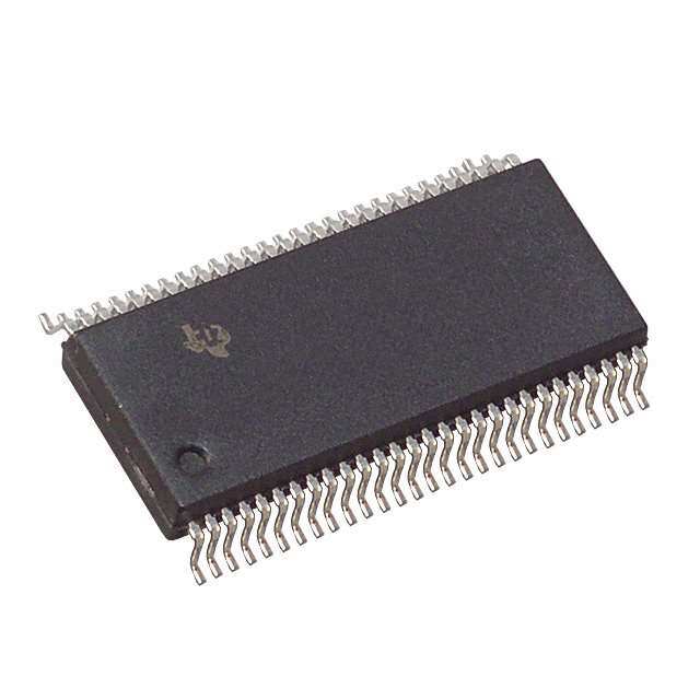
ICGOO电子元器件商城为您提供SN75976A1DL由Texas Instruments设计生产,在icgoo商城现货销售,并且可以通过原厂、代理商等渠道进行代购。 SN75976A1DL价格参考¥93.53-¥155.97。Texas InstrumentsSN75976A1DL封装/规格:接口 - 驱动器,接收器,收发器, 9/9 Transceiver Half RS422, RS485 56-SSOP。您可以下载SN75976A1DL参考资料、Datasheet数据手册功能说明书,资料中有SN75976A1DL 详细功能的应用电路图电压和使用方法及教程。
SN75976A1DL是Texas Instruments(德州仪器)生产的一款接口驱动器,属于多通道TTL至RS-422线路驱动器,常用于工业自动化、通信设备和数据采集系统中。该器件主要将TTL/CMOS电平转换为差分RS-422电平,支持高速、远距离的数据传输,具有较强的抗干扰能力。

典型应用场景包括:工业控制总线通信(如PLC之间的数据交换)、远程传感器信号传输、过程控制系统中的数字信号隔离与驱动、以及需要长距离稳定传输的串行通信系统。由于其具备高噪声抑制性能和可靠的数据传输能力,特别适用于电磁干扰较强或传输距离较远的工业环境。

此外,SN75976A1DL也常用于测试测量设备、楼宇自动化系统和电信基础设施中,作为关键的接口驱动元件,确保信号在复杂环境中仍能准确传输。其封装形式(如DL表示SOIC封装)适合PCB高密度布局,便于集成于紧凑型工业模块中。

总之,SN75976A1DL凭借其稳定性、抗干扰性和兼容性,广泛应用于需要可靠RS-422通信的工业与通信领域。
| 参数 | 数值 |
| 产品目录 | 集成电路 (IC)半导体 |
| 描述 | IC DIFF XCVR RS485 9-CH 56-SSOPRS-485接口IC 9-Channel Diff Transceiver |
| 产品分类 | |
| 品牌 | Texas Instruments |
| 产品手册 | |
| 产品图片 |
|
| rohs | 符合RoHS无铅 / 符合限制有害物质指令(RoHS)规范要求 |
| 产品系列 | 接口 IC,RS-485接口IC,Texas Instruments SN75976A1DL- |
| 数据手册 | |
| 产品型号 | SN75976A1DL |
| 产品目录页面 | |
| 产品种类 | RS-485接口IC |
| 传播延迟时间ns | 13.5 ns |
| 供应商器件封装 | 56-SSOP |
| 关闭 | Yes |
| 其它名称 | 296-9926-5 |
| 功能 | Transceiver |
| 包装 | 管件 |
| 协议 | RS485 |
| 单位重量 | 694.800 mg |
| 双工 | Half Duplex |
| 商标 | Texas Instruments |
| 安装类型 | 表面贴装 |
| 安装风格 | SMD/SMT |
| 封装 | Tube |
| 封装/外壳 | 56-BSSOP(0.295",7.50mm 宽) |
| 封装/箱体 | SSOP-56 |
| 工作温度 | 0°C ~ 70°C |
| 工作温度范围 | 0 C to + 70 C |
| 工作电源电压 | 5 V |
| 工厂包装数量 | 20 |
| 接收器滞后 | 45mV |
| 接收机数量 | 9 Receiver |
| 数据速率 | 20 Mb/s |
| 最大功率耗散 | 2500 mW |
| 最大工作温度 | + 70 C |
| 最小工作温度 | 0 C |
| 标准包装 | 20 |
| 激励器数量 | 9 Driver |
| 电压-电源 | 4.75 V ~ 5.25 V |
| 电源电流 | 60 mA |
| 类型 | 收发器 |
| 系列 | SN75976A |
| 输入电压 | 5 V |
| 输出电压 | 1.8 V |
| 输出电流 | 260 mA |
| 输出类型 | Differential |
| 驱动器/接收器数 | 9/9 |


- 商务部:美国ITC正式对集成电路等产品启动337调查
- 曝三星4nm工艺存在良率问题 高通将骁龙8 Gen1或转产台积电
- 太阳诱电将投资9.5亿元在常州建新厂生产MLCC 预计2023年完工
- 英特尔发布欧洲新工厂建设计划 深化IDM 2.0 战略
- 台积电先进制程称霸业界 有大客户加持明年业绩稳了
- 达到5530亿美元!SIA预计今年全球半导体销售额将创下新高
- 英特尔拟将自动驾驶子公司Mobileye上市 估值或超500亿美元
- 三星加码芯片和SET,合并消费电子和移动部门,撤换高东真等 CEO
- 三星电子宣布重大人事变动 还合并消费电子和移动部门
- 海关总署:前11个月进口集成电路产品价值2.52万亿元 增长14.8%


PDF Datasheet 数据手册内容提取
SN75976A, SN55976A 9-CHANNEL DIFFERENTIAL TRANSCEIVER SLLS218B – MAY 1995 – REVISED MAY 1997 (cid:1) Improved Speed and Package Replacement SN75976A DGG or DL for the SN75LBC976 SN55976A WD (cid:1) (TOP VIEW) Designed to Operate at up to 20 Million Data Transfers per Second (Fast-20 SCSI) (cid:1) GND 1 56 CDE2 Nine Differential Channels for the Data and BSR 2 55 CDE1 Control Paths of the Small Computer CRE 3 54 CDE0 Systems Interface (SCSI) and Intelligent 1A 4 53 9B+ Peripheral Interface (IPI) (cid:1) 1DE/RE 5 52 9B– SN75976A Packaged in Shrink 2A 6 51 8B+ Small-Outline Package with 25-Mil Terminal 2DE/RE 7 50 8B– Pitch (DL) and Thin Shrink Small-Outline 3A 8 49 7B+ Package with 20-Mil Terminal Pitch (DGG) 3DE/RE 9 48 7B– (cid:1) SN55976A Packaged in a 56-Pin Ceramic 4A 10 47 6B+ Flat Pack (WD) 4DE/RE 11 46 6B– (cid:1) Two Skew Limits Available VCC 12 45 VCC (cid:1) ESD Protection on Bus Terminals GND 13 44 GND Exceeds 12 kV GND 14 43 GND (cid:1) GND 15 42 GND Low Disabled Supply Current 8 mA Typ (cid:1) GND 16 41 GND Thermal Shutdown Protection GND 17 40 GND (cid:1) Positive- and Negative-Current Limiting VCC 18 39 VCC (cid:1) Power-Up/Down Glitch Protection 5A 19 38 5B+ 5DE/RE 20 37 5B– description 6A 21 36 4B+ 6DE/RE 22 35 4B– The SN75976A is an improved replacement for 7A 23 34 3B+ the industry’s first 9-channel RS-485 7DE/RE 24 33 3B– transceiver — the SN75LBC976. The A version 8A 25 32 2B+ offers improved switching performance, a smaller 8DE/RE 26 31 2B– package, and higher ESD protection. The 9A 27 30 1B+ SN75976A is offered in two versions. The ’976A2 9DE/RE 28 29 1B– skew limits of 4 ns for the differential drivers and 5 ns for the differential receivers complies with the recommended skew budget of the Fast-20 SCSI Terminals 13 through 17 and 40 through 44 are connected together to the package lead frame standard for data transfer rates up to 20 million and signal ground. transfers per second. The ’976A1 supports the Fast SCSI skew budget for 10 million transfers per second. The skew limit ensures that the propagation delay times, not only from channel-to-channel but from device-to-device, are closely matched for the tight skew budgets associated with high-speed parallel data buses. The patented thermal enhancements made to the 56-pin shrink small-outline package (SSOP) of the SN75976 have been applied to the new, thin shrink, small-outline package (TSSOP). The TSSOP package offers even less board area requirements than the SSOP while reducing the package height to 1 mm. This provides more board area and allows component mounting to both sides of the printed circuit boards for low-profile, space-restricted applications such as small form-factor hard disk drives. Please be aware that an important notice concerning availability, standard warranty, and use in critical applications of TexasInstruments semiconductor products and disclaimers thereto appears at the end of this data sheet. PRODUCTION DATA information is current as of publication date. Copyright 1997, Texas Instruments Incorporated Products conform to specifications per the terms of Texas Instruments standard warranty. Production processing does not necessarily include testing of all parameters. POST OFFICE BOX 655303 • DALLAS, TEXAS 75265 1
SN75976A, SN55976A 9-CHANNEL DIFFERENTIAL TRANSCEIVER SLLS218B – MAY 1995 – REVISED MAY 1997 description (continued) In addition to speed improvements, the ’976A can withstand electrostatic discharges exceeding 12 kV using the human-body model, and 600 V using the machine model of MIL-PRF-38535, Method 3015.7 on the RS-485 I/O terminals. This is six times the industry standard and provides protection from the noise that can be coupled into external cables. The other terminals of the device can withstand discharges exceeding 4 kV and 400 V respectively. Each of the nine channels of the ’976A typically meet or exceed the requirements of EIA RS-485 (1983) and ISO8482-1987/TIA TR30.2 referenced by American National Standard of Information (ANSI) Systems, X3.131-1994 (SCSI-2) standard, X2.277-1996 (Fast-20 Parallel Interface), and the Intelligent Peripheral Interface Physical Layer-ANSI X3.129-1986 standard. The SN75976A is characterized for operation over an ambient air temperature range of 0°C to 70°C. The SN55976A is characterized for operation over an ambient air temperature range of –55°C to 125°C. AVAILABLE OPTIONS Skew Limit PACKAGE† (ns) TTAA TSSOP SSOP CERAMIC FLAT PACK Driver Receiver (DGG) (DL) (WD) SN75976A1DGG SN75976A1DL 8 9 — SN75976A1DGGR SN75976A1DLR 00°°CC ttoo 7700°°CC SN75976A2DGG SN75976A2DL 4 5 — SN75976A2DGGR SN75976A2DLR 8 9 — — SN55976A1WD –5555°°CC ttoo 112255°°CC 4 5 — — SN55976A2WD †The R suffix indicates taped and reeled packages. 2 POST OFFICE BOX 655303 • DALLAS, TEXAS 75265
SN75976A, SN55976A 9-CHANNEL DIFFERENTIAL TRANSCEIVER SLLS218B – MAY 1995 – REVISED MAY 1997 Terminal Functions TERMINAL Loggic II//OO TTeerrmmiinnaattiioonn DDEESSCCRRIIPPTTIIOONN NAME NO. Level 1A to 9A 4,6,8,10, TTL I/O Pullup 1A to 9A carry data to and from the communication controller. 19,21,23, 25,27 1B– to 9B– 29,31,33, RS-485 I/O Pulldown 1B– to 9B– are the inverted data signals of the balanced pair to/from 35,37,.46, the bus. 48,50,52 1B+ to 9B+ 30,32,34, RS-485 I/O Pullup 1B+ to 9B+ are the noninverted data signals of the balanced pair to/from 36,38,47, the bus. 49,51,53 BSR 2 TTL Input Pullup BSR is the bit significant response. BSR disables receivers 1 through 8 and enables wired-OR drivers when BSR and DE/RE and CDE1 or CDE2 are high. Channel 9 is placed in a high-impedance state with BSR high. CDE0 54 TTL Input Pulldown CDE0 is the common driver enable 0. Its input signal enables all drivers when CDE0 and 1DE/RE – 9DE/RE are high. CDE1 55 TTL Input Pulldown CDE1 is the common driver enable 1. Its input signal enables drivers 1 to 4 when CDE1 is high and BSR is low. CDE2 56 TTL Input Pulldown CDE2 is the common driver enable 2. When CDE2 is high and BSR is low, drivers 5 to 8 are enabled. CRE 3 TTL Input Pullup CRE is the common receiver enable. When high, CRE disables receiver channels 5 to 9. 1DE/RE to 5,7,9,11, TTL Input Pullup 1DE/RE–9DE/RE are direction controls that transmit data to the bus when 9DE/RE 20,22,24, it and CDE0 are high. Data is received from the bus when 26,28 1DE/RE–9DE/RE and CRE and BSR are low and CDE1 and CDE2 are low. GND 1,13,14, NA Power NA GND is the circuit ground. All GND terminals except terminal 1 are 15,16,17, physically tied to the die pad for improved thermal conductivity.† 40,41,42, 43,44 VCC 12,18,39, NA Power NA Supply voltage 45 †Terminal 1 must be connected to signal ground for proper operation. POST OFFICE BOX 655303 • DALLAS, TEXAS 75265 3
SN75976A, SN55976A 9-CHANNEL DIFFERENTIAL TRANSCEIVER SLLS218B – MAY 1995 – REVISED MAY 1997 logic diagram (positive logic) 54 CDE0 55 CDE1 2 BSR 30 4 1B+ 1A 29 1B– 5 1DE/RE 6 32 2A 2B+ 7 Channel 2 31 2DE/RE 2B– 8 34 3A 3B+ 9 Channel 3 33 3DE/RE 3B– 10 36 4A 4B+ 11 Channel 4 35 4DE/RE 4B– 56 CDE2 3 CRE 38 19 5B+ 5A 37 5B– 20 5DE/RE 21 47 6A 6B+ 22 Channel 6 46 6DE/RE 6B– 23 49 7A 7B+ 24 Channel 7 48 7DE/RE 7B– 25 51 8A 8B+ 26 Channel 8 50 8DE/RE 8B– 2 3 54 27 BSR BSR CRE CDE0 53 9B+ 9A 52 9B– 28 9DE/RE 4 POST OFFICE BOX 655303 • DALLAS, TEXAS 75265
SN75976A, SN55976A 9-CHANNEL DIFFERENTIAL TRANSCEIVER SLLS218B – MAY 1995 – REVISED MAY 1997 schematics of inputs and outputs DE/RE, CRE, BSR, AND CDE0, CDE1, AND CDE2 Inputs A Inputs VCC VCC 100 kW 1 kW 1 kW Input Input 100 kW 8 V 8 V B+ Input B– Input VCC VCC 100 kW 2 kW 2 kW 16 V 16 V 18 kW 18 kW Input Input 100 kW 4 kW 4 kW 16 V 16 V B+ AND B– Outputs VCC A Output VCC 2 kW 16 V 40 W 18 kW Output Output 8 V 4 kW 16 V POST OFFICE BOX 655303 • DALLAS, TEXAS 75265 5
SN75976A, SN55976A 9-CHANNEL DIFFERENTIAL TRANSCEIVER SLLS218B – MAY 1995 – REVISED MAY 1997 absolute maximum ratings over operating free-air temperature range (unless otherwise noted)† Supply voltage range, VCC (see Note 1) . . . . . . . . . . . . . . . . . . . . . . . . . . . . . . . . . . . . . . . . . . . . . . –0.3 V to 6 V Bus voltage range . . . . . . . . . . . . . . . . . . . . . . . . . . . . . . . . . . . . . . . . . . . . . . . . . . . . . . . . . . . . . . . . . . –10 V to 15 V Data I/O and control (A side) voltage range . . . . . . . . . . . . . . . . . . . . . . . . . . . . . . . . . . . . . –0.3 V to VCC +0.5 V Electrostatic discharge:B side and GND, Class 3, A: (see Note 2) . . . . . . . . . . . . . . . . . . . . . . . . . . . . . . . 12 kV B side and GND, Class 3, B: (see Note 2) . . . . . . . . . . . . . . . . . . . . . . . . . . . . . . . 400 V All terminals, Class 3, A: . . . . . . . . . . . . . . . . . . . . . . . . . . . . . . . . . . . . . . . . . . . . . . . 4 kV All terminals, Class 3, B: . . . . . . . . . . . . . . . . . . . . . . . . . . . . . . . . . . . . . . . . . . . . . 400 V Continuous total power dissipation (see Note 3) . . . . . . . . . . . . . . . . . . . . . . . . . . . . . . . . . . . . . . internally limited Storage temperature range, T . . . . . . . . . . . . . . . . . . . . . . . . . . . . . . . . . . . . . . . . . . . . . . . . . . . –65°C to 150°C stg Lead temperature 1,6 mm (1/16 inch) from case for 10 seconds . . . . . . . . . . . . . . . . . . . . . . . . . . . . . . . 260°C †Stresses beyond those listed under “absolute maximum ratings” may cause permanent damage to the device. These are stress ratings only, and functional operation of the device at these or any other conditions beyond those indicated under “recommended operating conditions” is not implied. Exposure to absolute-maximum-rated conditions for extended periods may affect device reliability. NOTES: 1. All voltage values are with respect to the GND terminals. 2. This absolute maximum rating is tested in accordance with MIL-PRF-38535, Method 3015.7. 3. The maximum operating junction temperature is internally limited. Use the Dissipation Rating Table to operate below this temperature. DISSIPATION RATING TABLE PACKAGE TA ≤ 25°C OPAEBROAVTEIN TGA F =A 2C5T°OCR‡ POWTAE R= 7R0A°TCING POTWAE =R 1 R2A5°TCING DGG 2500 mW 20 mW/°C 1600 mW — DL 2500 mW 20 mW/°C 1600 mW — WD 1300 mW 10.5 mW/°C 827 mW 250 mW ‡This is the inverse of the junction-to-ambient thermal resistance when board-mounted and with no air flow. package thermal characteristics MIN NOM MAX UNIT DGG, board-mounted, no air flow 50 °C/W JJuunnccttiioonn-ttoo-aammbbiieenntt tthheerrmmaall rreessiissttaannccee, RRqq JJAA DL, board-mounted, no air flow 50 °C/W Junction-to-ambient thermal resistance, Rq JA WD 95.4 °C/W DGG 27 °C/W JJuunnccttiioonn-ttoo-ccaassee tthheerrmmaall rreessiissttaannccee, RRqq JJCC DL 12 °C/W Junction-to-case thermal resistance, Rq JC WD 5.67 °C/W Thermal-shutdown junction temperature, TJS 165 °C 6 POST OFFICE BOX 655303 • DALLAS, TEXAS 75265
SN75976A, SN55976A 9-CHANNEL DIFFERENTIAL TRANSCEIVER SLLS218B – MAY 1995 – REVISED MAY 1997 recommended operating conditions MIN NOM MAX UNIT Supply voltage, VCC 4.75 5 5.25 V High-level input voltage, VIH Except nB+, nB–† 2 V Low-level input voltage, VIL Except nB+, nB–† 0.8 V 12 V VVoollttaaggee aatt aannyy bbuuss tteerrmmiinnaall ((sseeppaarraatteellyy oorr ccoommmmoonn-mmooddee)), VVOO, VVII, oorr VVIICC nnBB++ oorr nnBB – –7 V Driver –60 mA HHiigghh-lleevveell oouuttppuutt ccuurrrreenntt, IIOOHH Receiver –8 mA Driver 60 mA LLooww-lleevveell oouuttppuutt ccuurrrreenntt, IIOOLL Receiver 8 mA Operating case temperature, TC SN75976A 0 125 °C SN75976A 0 70 °C OOppeerraattiinngg ffrreeee-aaiirr tteemmppeerraattuurree, TTAA SN55976A –55 125 °C †n = 1 – 9 POST OFFICE BOX 655303 • DALLAS, TEXAS 75265 7
SN75976A, SN55976A 9-CHANNEL DIFFERENTIAL TRANSCEIVER SLLS218B – MAY 1995 – REVISED MAY 1997 electrical characteristics over recommended operating free-air temperature range (unless otherwise noted) SN55976A SN75976A PPAARRAAMMEETTEERR TTEESSTT CCOONNDDIITTIIOONNSS UUNNIITT MIN TYP† MAX MIN TYP† MAX S1 to A, VT = 5 V, See Figure 1 0.7 1 1.8 V VODH Dlleervviveeell oor uudttipffeuurtt evvnootllittaaalgg heeigh- STC1 t≥o 2B5,°C SVTee = F 5ig Vu,re 1 1 1.4 V S1 to B, VT = 5 V, 0.7 0.8 V See Figure 1 STC1 t≥o 2A5,°C SVTee = F 5ig Vu,re 1 0.7 –1.4 –1 –1.4 V DDriiver ddiifffferenttiiall llow- VODL lleevveell oouuttpuutt vvoollttaaggee S1 to B, VT = 5 V, See Figure 1 0.7 –1.8 –1 –1.8 V S1 to A, VT = 5 V, –0.8 –1.4 –0.8 –1.4 V See Figure 1 VOOHH Haaggigeeh-level output volt- AIO sHid =e ,– 8 mA VSIeDe =F i2g0u0re m 3V, 4 4.5 4 4.5 V B side, VT = 5 V, See Figure 1 3 3 V VOOLL Laaoggwee-level output volt- AIO sHid =e ,8 mA VSIeDe =F i–g2u0re0 3mV, 0.6 0.8 0.6 0.8 V A side, VT = 5 V, See Figure 1 1 1 V Receiver positive-go- VIT+ ing differential input IOH = –8 mA, See Figure 3 0.2 0.2 V threshold voltage Receiver negative- VIT– going differential input IOL = 8 mA, See Figure 3 –0.2 –0.2 V threshold voltage Receiver input Vhys hysteresis VCC = 5 V, TA = 25°C 24 45 24 45 mV (VIT+– VIT–) VIH = 12 V, VCC = 5 V, Other input at 0 V 0.4 1 0.4 1 mA VIH = 12 V, VCC = 0, Other input at 0 V 0.5 1 0.5 1 mA IIII BBuuss iinnppuutt ccuurrrreenntt VIH = –7 V, VCC = 5 V, Other input at 0 V –0.4 –0.8 –0.4 –0.8 mA VIH = –7 V, VCC = 0, Other input at 0 V –0.3 –0.8 –0.3 –0.8 mA Higgh-level input cur- A, BSR, DE/RE, and CRE, VIH = 2 V –100 –100 m A IIIIHH rent CDE0, CDE1, and CDE2, VIH = 2V 100 100 m A A, BSR, DE/RE, and CRE, VIL = 0.8 V –100 –100 m A IIIILL LLooww-lleevveell iinnppuutt ccuurrrreenntt CDE1, CDE1, and CDE2, VIL = 0.8 V 100 100 m A Short circuit output IOS current nB+ or nB– ±260 ±260 mA Higgh-impedance-state A See IIH and IIL See IIH and IIL IIOOZZ output current nB+ or nB– See II See II Disabled 10 10 mA ICC Supply current All drivers enabled, no load 60 60 mA All receivers enabled, no load 45 45 mA CO Output capacitance nB+ or nB– to GND 18 18 25 pF Power dissipation Receiver 40 40 pF CCpdd ccaappaacciittaannccee (see Note 4) Driver 100 100 pF †All typical values are at VCC = 5 V, TA = 25°C. NOTE 4: Cpd determines the no-load dynamic supply current consumption, IS = CPD × VCC × f + ICC 8 POST OFFICE BOX 655303 • DALLAS, TEXAS 75265
SN75976A, SN55976A 9-CHANNEL DIFFERENTIAL TRANSCEIVER SLLS218B – MAY 1995 – REVISED MAY 1997 driver switching characteristics over recommended operating conditions (unless otherwise noted) SN75976A PPAARRAAMMEETTEERR TTEESSTT CCOONNDDIITTIIOONNSS UUNNIITT MIN TYP† MAX 2.5 13.5 ns ’976A1 VCC = 5 V, TC = 25°C 3 11 ns ttpdd Propaggation delayy time,, tPPHHLL or tPPLLHH VCC = 5 V, TC = 100°C 5 13 ns (see Figures 1 and 2) 4.5 11.5 ns ’976A2 VCC = 5 V, TC = 25°C 5 9 ns VCC = 5 V, TC = 100°C 7 11 ns ttskk((lliim)) Skew limit,, maximum tpdd – minimum tpdd ’976A1 8 ns (see Note 5) ’976A2 4 ns tsk(p) Pulse skew, |tPHL – tPLH| 4 ns tf Fall time S1 to B, See Figure 2 4 ns tr Rise time See Figure 2 8 ns ten Enable time, control inputs to active output 50 ns tdis Disable time, control inputs to high-impedance output 100 ns tPHZ Propagation delay time, high-level to high-impedance output 17 100 ns tPLZ Propagation delay time, low-level to high-impedance output 25 100 ns SSeeee FFiigguurreess 55 aanndd 66 tPZH Propagation delay time, high-impedance to high-level output 17 50 ns tPZL Propagation delay time, high-impedance to low-level output 17 50 ns †All typical values are at VCC = 5 V, TA = 25°C. NOTE 5: This parameter is applicable at one VCC and operating temperature within the recommended operating conditions and to any two devices. driver switching characteristics over recommended operating conditions (unless otherwise noted) SN55976A PPAARRAAMMEETTEERR TTEESSTT CCOONNDDIITTIIOONNSS UUNNIITT MIN TYP† MAX ttpdd Propaggation delayy time,, tPPHHLL or tPPLLHH ’976A1 VCC = 5 V, TA = 25°C 15 ns (see Figures 1 and 2) ’976A2 VCC = 5 V, TA = 25°C 13.5 ns ttskk((lliim)) Skew limit,, maximum tpdd – minimum tpdd ’976A1 8 ns (see Note 5) ’976A2 4 ns tsk(p) Pulse skew, |tPHL – tPLH| 4 ns tf Fall time S1 to B, See Figure 2 4 ns tr Rise time See Figure 2 8 ns ten Enable time, control inputs to active output 60 ns tdis Disable time, control inputs to high-impedance output 140 ns tPHZ Propagation delay time, high-level to high-impedance output 120 ns tPLZ Propagation delay time, low-level to high-impedance output 120 ns SSeeee FFiigguurreess 55 aanndd 66 tPZH Propagation delay time, high-impedance to high-level output 60 ns tPZL Propagation delay time, high-impedance to low-level output 60 ns †All typical values are at VCC = 5 V, TA = 25°C. NOTE 5. This parameter is applicable at one VCC and operating temperature within the recommended operating conditions and to any two devices. POST OFFICE BOX 655303 • DALLAS, TEXAS 75265 9
SN75976A, SN55976A 9-CHANNEL DIFFERENTIAL TRANSCEIVER SLLS218B – MAY 1995 – REVISED MAY 1997 receiver switching characteristics over recommended operating conditions (unless otherwise noted) SN75976A PPAARRAAMMEETTEERR TTEESSTT CCOONNDDIITTIIOONNSS UUNNIITT MIN TYP† MAX ’976A1 7.5 16.5 ns ttpdd Propaggation delayy time,, tPPHHLL or tPPLLHH 8.5 14.5 ns (see Figures 3 and 4) ’976A2 VCC = 5 V, TC = 25°C 8.6 13.6 ns VCC = 5 V, TC = 100°C 9 14 ns ttskk((lliim)) Skew limit,, maximum tpdd – minimum tpdd ’976A1 9 ns (see Note 5) ’976A2 5 ns tsk(p) Pulse skew, |tPHL – tPLH| 0.6 4 ns tt Transition time (tr or tf) See Figure 4 2 ns ten Enable time, control inputs to active output 50 ns tdis Disable time, control inputs to high-impedance output 60 ns tPHZ Propagation delay time, high-level to high-impedance output 60 ns tPLZ Propagation delay time, low-level to high-impedance output 50 ns SSeeee FFiigguurreess 77 aanndd 88 tPZH Propagation delay time, high-impedance to high-level output 50 ns tPZL Propagation delay time, high-impedance to low-level output 50 ns †All typical values are at VCC = 5 V, TA = 25°C. NOTE 5. This parameter is applicable at one VCC and operating temperature within the recommended operating conditions and to any two devices. receiver switching characteristics over recommended operating conditions (unless otherwise noted) SN55976A PPAARRAAMMEETTEERR TTEESSTT CCOONNDDIITTIIOONNSS UUNNIITT MIN TYP† MAX ttpdd Propaggation delayy time,, tPPHHLL or tPPLLHH ’976A1 VCC = 5 V, TA = 25°C 19 ns (see Figures 3 and 4) ’976A2 VCC = 5 V, TA = 25°C 16 ns ttskk((lliim)) Skew limit,, maximum tpdd – minimum tpdd ’976A1 9 ns (see Note 5) ’976A2 5 ns tsk(p) Pulse skew, |tPHL – tPLH| 0.6 4 ns tt Transition time (tr or tf) See Figure 4 2 ns ten Enable time, control inputs to active output 70 ns tdis Disable time, control inputs to high-impedance output 80 ns tPHZ Propagation delay time, high-level to high-impedance output 80 ns tPLZ Propagation delay time, low-level to high-impedance output 70 ns SSeeee FFiigguurreess 77 aanndd 88 tPZH Propagation delay time, high-impedance to high-level output 70 ns tPZL Propagation delay time, high-impedance to low-level output 70 ns †All typical values are at VCC = 5 V, TA = 25°C. NOTE 5. This parameter is applicable at one VCC and operating temperature within the recommended operating conditions and to any two devices. 10 POST OFFICE BOX 655303 • DALLAS, TEXAS 75265
SN75976A, SN55976A 9-CHANNEL DIFFERENTIAL TRANSCEIVER SLLS218B – MAY 1995 – REVISED MAY 1997 PARAMETER MEASUREMENT INFORMATION SN75976A = 5 V SN55976A = 4.5 V A B 165 W B+ S1 IO II 15 pF 165 W 375 W A Input VOD 75 W (see Note A) VI VO 375 W IO B– S2 † VO 15 pF †CDE0 and DE/RE are at 2 V, BSR is at 0.8 V and, for the SN75976A only, all others are open. ‡For the SN75976A only, all nine drivers are enabled, similarly loaded, and switching. Figure 1. Driver Test Circuit, Currents, and Voltages‡ 3 V Input 1.5 V 1.5 V 0 V tPLH tPHL VOD(H) 90% 90% Output, VOD 0V 0V S1 to A or B 10% 10% VOD(L) tr tf Figure 2. Driver Delay and Transition Time Test Waveforms Input B+ Generator 50 W (see Note A) IO VID Output Generator Input B– 50 W VO CL = 15 pF (see Note A) † †CDE0, CDE1, CDE2, BSR, CRE, and DE/RE at 0.8 V ‡For the SN75976A only, all nine receivers are enabled and switching. Figure 3. Receiver Propagation Delay and Transition Time Test Circuit‡ NOTES: A. All input pulses are supplied by a generator having the following characteristics: tr ≤ 6 ns, tf ≤ 6 ns, PRR ≤ 1 MHz, duty cycle = 50%, ZO = 50 W . B. All resistances are in W and ± 5%, unless otherwise indicated. C. All capacitances are in pF and ± 10%, unless otherwise indicated. D. All indicated voltages are ± 10 mV. POST OFFICE BOX 655303 • DALLAS, TEXAS 75265 11
SN75976A, SN55976A 9-CHANNEL DIFFERENTIAL TRANSCEIVER SLLS218B – MAY 1995 – REVISED MAY 1997 PARAMETER MEASUREMENT INFORMATION Input B– 3 V 1.5 V 1.5 V Input B+ 0 V tPLH tPHL VOH 90% 90% Output 1.4 V 1.4 V 10% 10% VOL tr tf Figure 4. Receiver Delay and Transition Time Waveforms 4.5 V A B 165 W B+ S1 50 pF 165 W 375 W A 0 V or 3 V VOD 75 W 375 W B– S2 DE/RE See Table 1 50 pF† Input †Includes probe and jig capacitance in two places. Figure 5. Driver Enable and Disable Time Test Circuit Table 1. Enabling For Driver Enable And Disable Time DRIVER BSR CDE0 CDE1 CDE2 CRE 1 – 8 H H L L X 9 L H H H H 3 V Input, DE/RE 1.5 V 1.5 V 0 V tPZH tPHZ VOD(H) A at 3V Output, VOD 0 V 0 V S1 to B ~ –1 V tPZL tPLZ ~ 1 V A at 0V Output, VOD 0 V 0 V S1 to A VOD(L) Figure 6. Driver Enable Time Waveforms NOTES: A. All input pulses are supplied by a generator having the following characteristics: tr ≤ 6 ns, tf ≤ 6 ns, PRR ≤ 1 MHz, duty cycle = 50%, ZO = 50 W . B. All resistances are in W and ± 5%, unless otherwise indicated. C. All capacitances are in pF and ± 10%, unless otherwise indicated. D. All indicated voltages are ± 10 mV. 12 POST OFFICE BOX 655303 • DALLAS, TEXAS 75265
SN75976A, SN55976A 9-CHANNEL DIFFERENTIAL TRANSCEIVER SLLS218B – MAY 1995 – REVISED MAY 1997 PARAMETER MEASUREMENT INFORMATION VT 620 W B+ 0 V or 3 V A Output DE/RE Input † 3 V or 0 V B– 40 pF‡ †CDE0 is high, CDE1, CDE2, BSR, and CRE are low and, for the SN75976A only, all others are open. ‡Includes probe and jig capacitance. Figure 7. Receiver Enable and Disable Time Test Circuit 3 V Input 1.4 V 1.4 V 0 V tPLZ tPZL B+ at 0 V Output 1.4 V 1.4 V B– at 3 V VT = VCC VOD Indeterminate tPHZ tPZH 1.4 V 1.4 V B+ at 3 V Output B– at 0 V VT = 0 Indeterminate VOD Figure 8. Receiver Enable and Disable Time Waveforms NOTES: A. All input pulses are supplied by a generator having the following characteristics: tr ≤ 6 ns, tf ≤ 6 ns, PRR ≤ 1 MHz, duty cycle = 50%, ZO = 50 W . B. All resistances are in W and ± 5%, unless otherwise indicated. C. All capacitances are in pF and ± 10%, unless otherwise indicated. D. All indicated voltages are ± 10 mV. POST OFFICE BOX 655303 • DALLAS, TEXAS 75265 13
SN75976A, SN55976A 9-CHANNEL DIFFERENTIAL TRANSCEIVER SLLS218B – MAY 1995 – REVISED MAY 1997 TYPICAL CHARACTERISTICS AVERAGE SUPPLY CURRENT LOGIC INPUT CURRENT vs vs FREQUENCY INPUT VOLTAGE 250 –30 A, DE/RE,CRE,BSR A m –25 – 200 A ent m– y Curr 150 urrent –20 pl C up ut –15 S p rage 100 gic In e o –10 Á– AvÁ 9 Drivers – L ÁCÁ50 II C –5 I ÁÁ 9 Receivers 0 0 0.001 0.01 0.1 1 10 100 0 1 2 3 4 5 f – Frequency – MHz VI – Input Voltage – V Figure 9 Figure 10 BUS DRIVER INPUT CURRENT LOW-LEVEL OUTPUT VOLTAGE vs vs INPUT VOLTAGE LOW-LEVEL OUTPUT CURRENT 15 2.5 V 10 – 2 e g A a – m Volt nt 5 ut 1.5 e p Curr Out nput 0 Level 1 – I w- II Lo ÁÁ– –5 L 0.5 O ÁVÁ –10 0 –20 –15 –10 –5 0 5 10 15 20 0 10 20 30 40 50 60 70 80 90 100 VI – Input Voltage – V IOL – Low-Level Output Current – mA Figure 11 Figure 12 14 POST OFFICE BOX 655303 • DALLAS, TEXAS 75265
SN75976A, SN55976A 9-CHANNEL DIFFERENTIAL TRANSCEIVER SLLS218B – MAY 1995 – REVISED MAY 1997 TYPICAL CHARACTERISTICS DRIVER DRIVER HIGH-LEVEL OUTPUT VOLTAGE AVERAGE DIFFERENTIAL OUTPUT VOLTAGE vs vs HIGH-LEVEL OUTPUT CURRENT AVERAGE CASE TEMPERATURE 4 2.5 V VOD(L), VCC = 5.25 V – 3.5 e ge – V 3 Voltag 2 olta put V 2.5 ut ut O 1.5 Outp 2 ntial el ere VOD(L), VCC = 4.75 V Lev 1.5 Diff 1 h- e VOD(H), VCC = 5.25 V g g Á– HiÁ 1 vera VOD(H), VCC = 4.75 V ÁHÁ ÁAÁ0.5 O – ÁVÁ 0.5 Á|DÁ O S1 to Position B (see Figure 1) ÁVÁ 0 | 0 0 –20 –40 –60 –80 –100 0 20 40 60 80 100 120 140 IOH – High-Level Output Current – mA TC – Average Case Temperature – °C Figure 13 Figure 14 RECEIVER DRIVER PROPAGATION DELAY TIME PROPAGATION DELAY TIME vs vs CASE TEMPERATURE CASE TEMPERATURE 16 14 VCC = 5 V, S1 to Position B (see Figure 1) 14 tPHL(max) 12 s s n n – – tPHL(max) me 12 tPLH(max) me 10 y Ti tPHL(min) y Ti a a el 10 el 8 D D on tPLH(min) on tPLH(max) agati 8 agati 6 tPLH(min) tPHL(min) p p o o Pr 6 Pr 4 – – d d p (Data Extracted From 7 Wafer Lots) p t 4 t 2 VCC = 5 V Data Extracted From 7 Wafer Lots 2 0 0 20 40 60 80 100 120 140 0 20 40 60 80 100 120 140 TC – Case Temperature – °C TC – Case Temperature – °C Figure 15 Figure 16 POST OFFICE BOX 655303 • DALLAS, TEXAS 75265 15
SN75976A, SN55976A 9-CHANNEL DIFFERENTIAL TRANSCEIVER SLLS218B – MAY 1995 – REVISED MAY 1997 TYPICAL CHARACTERISTICS DRIVER OUTPUT CURRENT vs SUPPLY VOLTAGE 100 TA = 25°C 80 IOH 60 A m – 40 nt e rr 20 u C ut 0 p ut O – –20 O I –40 –60 IOL –80 0 1 2 3 4 5 6 VCC – Supply Voltage – V Figure 17 16 POST OFFICE BOX 655303 • DALLAS, TEXAS 75265
SN75976A, SN55976A 9-CHANNEL DIFFERENTIAL TRANSCEIVER SLLS218B – MAY 1995 – REVISED MAY 1997 APPLICATION INFORMATION Table 2. Typical Signal and Terminal Assignments SIGNAL TERMINAL SCSI DATA SCSI CONTROL IPI DATA IPI CONTROL CDE0 54 DIFFSENSE DIFFSENSE VCC VCC CDE1 55 GND GND XMTA, XMTB GND CDE2 56 GND GND XMTA, XMTB SLAVE/MASTER BSR 2 GND GND GND, BSR GND CRE 3 GND GND GND VCC 1A 4 DB0, DB8 ATN AD7, BD7 NOT USED 1DE/RE 5 DBE0, DBE8 INIT EN GND GND 2A 6 DB1, DB9 BSY AD6, BD6 NOT USED 2DE/RE 7 DBE1, DBE9 BSY EN GND GND 3A 8 DB2, DB10 ACK AD5, BD5 SYNC IN 3DE/RE 9 DBE2, DBE10 INIT EN GND GND 4A 10 DB3, DB11 RST AD4, BD4 SLAVE IN 4DE/RE 11 DBE3, DBE11 GND GND GND 5A 19 DB4, DB12 MSG AD3, BD3 NOT USED 5DE/RE 20 DBE4, DBE12 TARG EN GND GND 6A 21 DB5, DB13 SEL AD2, BD2 SYNC OUT 6DE/RE 22 DBE5, DBE13 SEL EN GND GND 7A 23 DB6, DB14 C/D AD1, BD1 MASTER OUT 7DE/RE 24 DBE6, DBE14 TARG EN GND GND 8A 25 DB7, DB15 REQ AD0, BD0 SELECT OUT 8DE/RE 26 DBE7, DBE15 TARG EN GND GND 9A 27 DBP0, DBP1 I/O AP, BP ATTENTION IN 9DE/RE 28 DBPE0, DBPE1 TARG EN XMTA, XMTB VCC ABBREVIATIONS: DBn = data bit n, where n = (0,1,...,15) DBEn = data bit n enable, where n = (0,1,...,15) DBP0 = parity bit for data bits 0 through 7 or IPI bus A DBPE0 = parity bit enable for P0 DBP1 = parity bit for data bits 8 through 15 or IPI bus B DBPE1 = parity bit enable for P1 ADn or BDn = IPI Bus A – Bit n (ADn) or Bus B – Bit n (BDn), where n = (0,1,...,7) AP or BP = IPI parity bit for bus A or bus B XMTA or XMTB = transmit enable for IPI bus A or B BSR = bit significant response INIT EN = common enable for SCSI initiator mode TARG EN = common enable for SCSI target mode NOTE A: Signal inputs are shown as active high. When only active-low inputs are available, logic inversion is accomplished by reversing the B+ and B– connector terminal assignments. POST OFFICE BOX 655303 • DALLAS, TEXAS 75265 17
SN75976A, SN55976A 9-CHANNEL DIFFERENTIAL TRANSCEIVER SLLS218B – MAY 1995 – REVISED MAY 1997 APPLICATION INFORMATION Function Tables RECEIVER DRIVER B+ B+ A A B– B– INPUTS OUTPUT INPUT OUTPUTS B+† B–† A A B+ B– L H L L L H H L H H H L TRANSCEIVER DRIVER WITH ENABLE B+ A B+ B– A DE/RE B– DE/RE INPUTS OUTPUTS INPUTS OUTPUTS DE/RE A B+† B–† A B+ B– DE/RE A B+ B– L – L H L – – L L Z Z L – H L H – – L H Z Z H L – – – L H H L L H H H – – – H L H H H L WIRED-OR DRIVER TWO-ENABLE INPUT DRIVER B+ A A B– B+ B– DE/RE INPUT OUTPUTS INPUTS OUTPUTS A B+ B– DE/RE A B+ B– L Z Z L L Z Z H H L L H H L H L L H H H H L H = high level, L = low level, X = irrelevant, Z = high impedance (off) †An H in this column represents a voltage of 200 mV or higher than the other bus input. An L represents a voltage of 200 mV or lower than the other bus input. Any voltage less than 200 mV results in an indeterminate receiver output. 18 POST OFFICE BOX 655303 • DALLAS, TEXAS 75265
SN75976A, SN55976A 9-CHANNEL DIFFERENTIAL TRANSCEIVER SLLS218B – MAY 1995 – REVISED MAY 1997 APPLICATION INFORMATION VCC VCC SCSI SCSI 620 W † Connector 620 W † Connector nB+ nB+ nA + nA – I/O nB– I/O nB– – + EN EN nDE/RE nDE/RE (a) ACTIVE-HIGH BIDIRECTIONAL I/O (b) ACTIVE-LOW BIDIRECTIONAL I/O WITH SEPARATE ENABLE WITH SEPARATE ENABLE VCC VCC VCC SCSI SCSI 620 W † Connector 620 W † Connector 620 W † nB+ I nB+ I nA nB– + O‡ nA nB– + – – O EN nDE/RE nDE/RE (d) SEPARATE ACTIVE-HIGH INPUT, OUTPUT, (c) WIRED-OR DRIVER AND ACTIVE-HIGH INPUT AND ENABLE VCC VCC SCSI SCSI 620 W † Connector 620 W † Connector nB+ I nB+ nA – O‡ nA nB– – I nB– + + O EN nDE/RE nDE/RE 620 W (f) WIRED-OR DRIVER AND ACTIVE-LOW INPUT (e) SEPARATE ACTIVE-LOW INPUT AND OUTPUT AND ACTIVE-HIGH ENABLE †When 0 is open drain ‡Must be open-drain or 3-state output NOTE A: The BSR, CRE, A, and DE/RE inputs have internal pullup resistors. CDE0, CDE1, and CDE2 have internal pulldown resistors. Figure 18. Typical SCSI Transceiver Connections POST OFFICE BOX 655303 • DALLAS, TEXAS 75265 19
SN75976A, SN55976A 9-CHANNEL DIFFERENTIAL TRANSCEIVER SLLS218B – MAY 1995 – REVISED MAY 1997 APPLICATION INFORMATION channel logic configurations with control input logic The following logic diagrams show the positive-logic representation for all combinations of control inputs. The control inputs are from MSB to LSB; the BSR, CDE0, CDE1, CDE2, and CRE bit values are shown below the diagrams. Channel 1 is at the top of the logic diagrams; channel 9 is at the bottom of the logic diagrams. Hi-Z Hi-Z Hi-Z Hi-Z Hi-Z Hi-Z Figure 19. 00000 Figure 20. 00001 Figure 21. 00010 Figure 22. 00011 Figure 23. 00100 20 POST OFFICE BOX 655303 • DALLAS, TEXAS 75265
SN75976A, SN55976A 9-CHANNEL DIFFERENTIAL TRANSCEIVER SLLS218B – MAY 1995 – REVISED MAY 1997 APPLICATION INFORMATION Hi-Z Hi-Z Hi-Z Hi-Z Hi-Z Hi-Z Figure 24. 00101 Figure 25. 00110 Figure 26. 00111 Figure 28. 01001 Figure 27. 01000 POST OFFICE BOX 655303 • DALLAS, TEXAS 75265 21
SN75976A, SN55976A 9-CHANNEL DIFFERENTIAL TRANSCEIVER SLLS218B – MAY 1995 – REVISED MAY 1997 APPLICATION INFORMATION Figure 32. 01101 Figure 33. 01110 Figure 29. 01010 Figure 30. 01011 Figure 31. 01100 22 POST OFFICE BOX 655303 • DALLAS, TEXAS 75265
SN75976A, SN55976A 9-CHANNEL DIFFERENTIAL TRANSCEIVER SLLS218B – MAY 1995 – REVISED MAY 1997 APPLICATION INFORMATION Hi-Z Hi-Z Hi-Z Hi-Z Hi-Z Hi-Z Hi-Z Hi-Z Hi-Z Hi-Z Hi-Z Hi-Z Hi-Z Figure 34. 01111 Figure 35. 10000 and 10001 Hi-Z Hi-Z Hi-Z Hi-Z Hi-Z Hi-Z Figure 36. 10010 Figure 37. 10100 and 10011 and 10101 Hi-Z Figure 38. 10110 and 10111 POST OFFICE BOX 655303 • DALLAS, TEXAS 75265 23
SN75976A, SN55976A 9-CHANNEL DIFFERENTIAL TRANSCEIVER SLLS218B – MAY 1995 – REVISED MAY 1997 APPLICATION INFORMATION Hi-Z Figure 39. 11000 and 11001 Hi-Z Hi-Z Figure 40. 11010 Figure 41. 11100 and 11011 and 11101 Hi-Z Figure 42. 11110 and 11111 24 POST OFFICE BOX 655303 • DALLAS, TEXAS 75265
SN75976A, SN55976A 9-CHANNEL DIFFERENTIAL TRANSCEIVER SLLS218B – MAY 1995 – REVISED MAY 1997 MECHANICAL INFORMATION DGG (R-PDSO-G**) PLASTIC SMALL-OUTLINE PACKAGE 48 PIN SHOWN PINS ** 48 56 64 DIM 0,27 0,50 0,08 M 0,17 A MAX 12,60 14,10 17,10 48 25 A MIN 12,40 13,90 16,90 6,20 8,30 6,00 7,90 0,15 NOM Gage Plane 1 24 A 0,25 0°–8° 0,75 0,50 Seating Plane 1,20 MAX 0,05 MIN 0,10 4040078/D 08/96 NOTES: B. All linear dimensions are in millimeters. C. This drawing is subject to change without notice. D. Falls within JEDEC MO-153 POST OFFICE BOX 655303 • DALLAS, TEXAS 75265 25
SN75976A, SN55976A 9-CHANNEL DIFFERENTIAL TRANSCEIVER SLLS218B – MAY 1995 – REVISED MAY 1997 MECHANICAL INFORMATION DL (R-PDSO-G**) PLASTIC SMALL-OUTLINE PACKAGE 48 PIN SHOWN PINS ** 28 48 56 DIM 0.380 0.630 0.730 A MAX (9,65) (16,00) (18,54) 0.025 (0,635) 0.370 0.620 0.720 0.012 (0,305) 0.005 (0,13) M A MIN (9,40) (15,75) (18,29) 0.008 (0,203) 48 25 0.006 (0,15) NOM 0.299 (7,59) 0.291 (7,39) 0.420 (10,67) 0.395 (10,03) Gage Plane 0.010 (0,25) 1 24 0°–8° 0.040 (1,02) A 0.020 (0,51) Seating Plane 0.004 (0,10) 0.110 (2,79) MAX 0.008 (0,20) MIN 4040048/B 02/95 NOTES: A. All linear dimensions are in inches (millimeters). B. This drawing is subject to change without notice. C. Body dimensions do not include mold flash or protrusion not to exceed 0.006 (0,15). 26 POST OFFICE BOX 655303 • DALLAS, TEXAS 75265
SN75976A, SN55976A 9-CHANNEL DIFFERENTIAL TRANSCEIVER SLLS218B – MAY 1995 – REVISED MAY 1997 MECHANICAL INFORMATION WD (R-GDFP-F**) CERAMIC DUAL FLATPACK 48 PIN SHOWN NO. OF A PINS** MIN MAX 0.630 0.730 48 (16,00) (18,54) 0.120 (3,05) 0.610 0.710 0.075 (1,91) 56 (15,49) (18,03) 0.005 (0,13) NOM 1.200 (30,50) 0.950 (24,13) 0.390 (9,91) 0.370 (9,40) 1 48 0.025 (0,635) A 0.010 (0,25) TYP 24 25 4040176/C 04/96 NOTES: A. All linear dimensions are in inches (millimeters). B. This drawing is subject to change without notice. C. This package can be hermetically sealed with a ceramic lid using glass frit. D. Index point is provided on cap for pin identification only E. Falls within MIL-STD-1835: GDFP1-F48 and JEDEC MO-146AA GDFP1-F56 and JEDEC MO-146AB POST OFFICE BOX 655303 • DALLAS, TEXAS 75265 27
PACKAGE OPTION ADDENDUM www.ti.com 6-Feb-2020 PACKAGING INFORMATION Orderable Device Status Package Type Package Pins Package Eco Plan Lead/Ball Finish MSL Peak Temp Op Temp (°C) Device Marking Samples (1) Drawing Qty (2) (6) (3) (4/5) 5962-9689301QXA ACTIVE CFP WD 56 1 TBD Call TI N / A for Pkg Type -55 to 125 5962-9689301QX A SNJ55976A1WD SN55976A1WD ACTIVE CFP WD 56 1 TBD Call TI N / A for Pkg Type -55 to 125 SN55976A1WD SN75976A1DGG ACTIVE TSSOP DGG 56 35 Green (RoHS NIPDAU Level-2-260C-1 YEAR SN75976A1 & no Sb/Br) SN75976A1DL ACTIVE SSOP DL 56 20 Green (RoHS NIPDAU Level-2-260C-1 YEAR SN75976A1 & no Sb/Br) SN75976A1DLG4 ACTIVE SSOP DL 56 20 Green (RoHS NIPDAU Level-2-260C-1 YEAR SN75976A1 & no Sb/Br) SN75976A1DLR ACTIVE SSOP DL 56 1000 Green (RoHS NIPDAU Level-2-260C-1 YEAR SN75976A1 & no Sb/Br) SN75976A2DGG ACTIVE TSSOP DGG 56 35 Green (RoHS NIPDAU Level-2-260C-1 YEAR 0 to 70 SN75976A2 & no Sb/Br) SN75976A2DGGG4 ACTIVE TSSOP DGG 56 35 Green (RoHS NIPDAU Level-2-260C-1 YEAR 0 to 70 SN75976A2 & no Sb/Br) SN75976A2DGGR ACTIVE TSSOP DGG 56 2000 Green (RoHS NIPDAU Level-2-260C-1 YEAR SN75976A2 & no Sb/Br) SN75976A2DL ACTIVE SSOP DL 56 20 Green (RoHS NIPDAU Level-2-260C-1 YEAR SN75976A2 & no Sb/Br) SN75976A2DLR ACTIVE SSOP DL 56 1000 Green (RoHS NIPDAU Level-2-260C-1 YEAR SN75976A2 & no Sb/Br) SNJ55976A1WD ACTIVE CFP WD 56 1 TBD Call TI N / A for Pkg Type -55 to 125 5962-9689301QX A SNJ55976A1WD (1) The marketing status values are defined as follows: ACTIVE: Product device recommended for new designs. LIFEBUY: TI has announced that the device will be discontinued, and a lifetime-buy period is in effect. NRND: Not recommended for new designs. Device is in production to support existing customers, but TI does not recommend using this part in a new design. PREVIEW: Device has been announced but is not in production. Samples may or may not be available. OBSOLETE: TI has discontinued the production of the device. Addendum-Page 1
PACKAGE OPTION ADDENDUM www.ti.com 6-Feb-2020 (2) RoHS: TI defines "RoHS" to mean semiconductor products that are compliant with the current EU RoHS requirements for all 10 RoHS substances, including the requirement that RoHS substance do not exceed 0.1% by weight in homogeneous materials. Where designed to be soldered at high temperatures, "RoHS" products are suitable for use in specified lead-free processes. TI may reference these types of products as "Pb-Free". RoHS Exempt: TI defines "RoHS Exempt" to mean products that contain lead but are compliant with EU RoHS pursuant to a specific EU RoHS exemption. Green: TI defines "Green" to mean the content of Chlorine (Cl) and Bromine (Br) based flame retardants meet JS709B low halogen requirements of <=1000ppm threshold. Antimony trioxide based flame retardants must also meet the <=1000ppm threshold requirement. (3) MSL, Peak Temp. - The Moisture Sensitivity Level rating according to the JEDEC industry standard classifications, and peak solder temperature. (4) There may be additional marking, which relates to the logo, the lot trace code information, or the environmental category on the device. (5) Multiple Device Markings will be inside parentheses. Only one Device Marking contained in parentheses and separated by a "~" will appear on a device. If a line is indented then it is a continuation of the previous line and the two combined represent the entire Device Marking for that device. (6) Lead/Ball Finish - Orderable Devices may have multiple material finish options. Finish options are separated by a vertical ruled line. Lead/Ball Finish values may wrap to two lines if the finish value exceeds the maximum column width. Important Information and Disclaimer:The information provided on this page represents TI's knowledge and belief as of the date that it is provided. TI bases its knowledge and belief on information provided by third parties, and makes no representation or warranty as to the accuracy of such information. Efforts are underway to better integrate information from third parties. TI has taken and continues to take reasonable steps to provide representative and accurate information but may not have conducted destructive testing or chemical analysis on incoming materials and chemicals. TI and TI suppliers consider certain information to be proprietary, and thus CAS numbers and other limited information may not be available for release. In no event shall TI's liability arising out of such information exceed the total purchase price of the TI part(s) at issue in this document sold by TI to Customer on an annual basis. OTHER QUALIFIED VERSIONS OF SN55976A, SN75976A : •Catalog: SN75976A •Enhanced Product: SN75976A-EP, SN75976A-EP •Military: SN55976A NOTE: Qualified Version Definitions: •Catalog - TI's standard catalog product •Enhanced Product - Supports Defense, Aerospace and Medical Applications Addendum-Page 2
PACKAGE OPTION ADDENDUM www.ti.com 6-Feb-2020 •Military - QML certified for Military and Defense Applications Addendum-Page 3
PACKAGE MATERIALS INFORMATION www.ti.com 10-Aug-2016 TAPE AND REEL INFORMATION *Alldimensionsarenominal Device Package Package Pins SPQ Reel Reel A0 B0 K0 P1 W Pin1 Type Drawing Diameter Width (mm) (mm) (mm) (mm) (mm) Quadrant (mm) W1(mm) SN75976A1DLR SSOP DL 56 1000 330.0 32.4 11.35 18.67 3.1 16.0 32.0 Q1 SN75976A2DGGR TSSOP DGG 56 2000 330.0 24.4 8.6 15.6 1.8 12.0 24.0 Q1 SN75976A2DLR SSOP DL 56 1000 330.0 32.4 11.35 18.67 3.1 16.0 32.0 Q1 PackMaterials-Page1
PACKAGE MATERIALS INFORMATION www.ti.com 10-Aug-2016 *Alldimensionsarenominal Device PackageType PackageDrawing Pins SPQ Length(mm) Width(mm) Height(mm) SN75976A1DLR SSOP DL 56 1000 367.0 367.0 55.0 SN75976A2DGGR TSSOP DGG 56 2000 367.0 367.0 45.0 SN75976A2DLR SSOP DL 56 1000 367.0 367.0 55.0 PackMaterials-Page2
MECHANICAL DATA MCFP010B – JANUARY 1995 – REVISED NOVEMBER 1997 WD (R-GDFP-F**) CERAMIC DUAL FLATPACK 48 LEADS SHOWN 0.120 (3,05) 0.009 (0,23) 0.075 (1,91) 0.004 (0,10) 1.130 (28,70) 0.870 (22,10) 0.370 (9,40) 0.390 (9,91) 0.370 (9,40) 0.250 (6,35) 0.370 (9,40) 0.250 (6,35) 1 48 0.025 (0,635) A 0.014 (0,36) 0.008 (0,20) 24 25 NO. OF 48 56 LEADS** 0.640 0.740 A MAX (16,26) (18,80) 0.610 0.710 A MIN (15,49) (18,03) 4040176/D 10/97 NOTES: A. All linear dimensions are in inches (millimeters). B. This drawing is subject to change without notice. C. This package can be hermetically sealed with a ceramic lid using glass frit. D. Index point is provided on cap for terminal identification only E. Falls within MIL STD 1835: GDFP1-F48 and JEDEC MO-146AA GDFP1-F56 and JEDEC MO-146AB • POST OFFICE BOX 655303 DALLAS, TEXAS 75265
None
PACKAGE OUTLINE DGG0056A TSSOP - 1.2 mm max height SCALE 1.200 SMALL OUTLINE PACKAGE C 8.3 SEATING PLANE TYP 7.9 A PIN 1 ID 0.1 C AREA 54X 0.5 56 1 14.1 2X 13.9 13.5 NOTE 3 28 29 0.27 B 6.2 56X 0.17 1.2 MAX 6.0 0.08 C A B (0.15) TYP 0.25 SEE DETAIL A GAGE PLANE 0.15 0.75 0 - 8 0.05 0.50 DETAIL A TYPICAL 4222167/A 07/2015 NOTES: 1. All linear dimensions are in millimeters. Any dimensions in parenthesis are for reference only. Dimensioning and tolerancing per ASME Y14.5M. 2. This drawing is subject to change without notice. 3. This dimension does not include mold flash, protrusions, or gate burrs. Mold flash, protrusions, or gate burrs shall not exceed 0.15 mm per side. 4. Reference JEDEC registration MO-153. www.ti.com
EXAMPLE BOARD LAYOUT DGG0056A TSSOP - 1.2 mm max height SMALL OUTLINE PACKAGE 56X (1.5) SYMM 1 56 56X (0.3) 54X (0.5) (R0.05) TYP SYMM 28 29 (7.5) LAND PATTERN EXAMPLE SCALE:6X SOOPLEDNEINRG MASK METAL MSOELTDAEL RU NMDAESRK SOOPLEDNEINRG MASK 0.05 MAX 0.05 MIN ALL AROUND ALL AROUND NON SOLDER MASK SOLDER MASK DEFINED DEFINED SOLDER MASK DETAILS 4222167/A 07/2015 NOTES: (continued) 5. Publication IPC-7351 may have alternate designs. 6. Solder mask tolerances between and around signal pads can vary based on board fabrication site. www.ti.com
EXAMPLE STENCIL DESIGN DGG0056A TSSOP - 1.2 mm max height SMALL OUTLINE PACKAGE 56X (1.5) SYMM 1 56 56X (0.3) 54X (0.5) (R0.05) TYP SYMM 28 29 (7.5) SOLDER PASTE EXAMPLE BASED ON 0.125 mm THICK STENCIL SCALE:6X 4222167/A 07/2015 NOTES: (continued) 7. Laser cutting apertures with trapezoidal walls and rounded corners may offer better paste release. IPC-7525 may have alternate design recommendations. 8. Board assembly site may have different recommendations for stencil design. www.ti.com
IMPORTANTNOTICEANDDISCLAIMER TI PROVIDES TECHNICAL AND RELIABILITY DATA (INCLUDING DATASHEETS), DESIGN RESOURCES (INCLUDING REFERENCE DESIGNS), APPLICATION OR OTHER DESIGN ADVICE, WEB TOOLS, SAFETY INFORMATION, AND OTHER RESOURCES “AS IS” AND WITH ALL FAULTS, AND DISCLAIMS ALL WARRANTIES, EXPRESS AND IMPLIED, INCLUDING WITHOUT LIMITATION ANY IMPLIED WARRANTIES OF MERCHANTABILITY, FITNESS FOR A PARTICULAR PURPOSE OR NON-INFRINGEMENT OF THIRD PARTY INTELLECTUAL PROPERTY RIGHTS. These resources are intended for skilled developers designing with TI products. You are solely responsible for (1) selecting the appropriate TI products for your application, (2) designing, validating and testing your application, and (3) ensuring your application meets applicable standards, and any other safety, security, or other requirements. These resources are subject to change without notice. TI grants you permission to use these resources only for development of an application that uses the TI products described in the resource. Other reproduction and display of these resources is prohibited. No license is granted to any other TI intellectual property right or to any third party intellectual property right. TI disclaims responsibility for, and you will fully indemnify TI and its representatives against, any claims, damages, costs, losses, and liabilities arising out of your use of these resources. TI’s products are provided subject to TI’s Terms of Sale (www.ti.com/legal/termsofsale.html) or other applicable terms available either on ti.com or provided in conjunction with such TI products. TI’s provision of these resources does not expand or otherwise alter TI’s applicable warranties or warranty disclaimers for TI products. Mailing Address: Texas Instruments, Post Office Box 655303, Dallas, Texas 75265 Copyright © 2020, Texas Instruments Incorporated