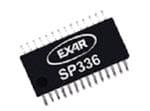
ICGOO在线商城 > 集成电路(IC) > 接口 - 驱动器,接收器,收发器 > SP336EEY-L
 Datasheet下载
- 型号: SP336EEY-L
- 制造商: Exar
- 库位|库存: xxxx|xxxx
- 要求:
| 数量阶梯 | 香港交货 | 国内含税 |
| +xxxx | $xxxx | ¥xxxx |
查看当月历史价格
查看今年历史价格
SP336EEY-L产品简介:
ICGOO电子元器件商城为您提供SP336EEY-L由Exar设计生产,在icgoo商城现货销售,并且可以通过原厂、代理商等渠道进行代购。 SP336EEY-L价格参考¥54.51-¥54.51。ExarSP336EEY-L封装/规格:接口 - 驱动器,接收器,收发器, 全 收发器 4/4 RS232,RS422,RS485 28-TSSOP。您可以下载SP336EEY-L参考资料、Datasheet数据手册功能说明书,资料中有SP336EEY-L 详细功能的应用电路图电压和使用方法及教程。
MaxLinear, Inc. 的 SP336EEY-L 是一款接口驱动器、接收器和收发器,广泛应用于需要高效数据传输和信号处理的场景。以下是该型号的主要应用场景:

1. 工业自动化
   用于工业控制设备中,如可编程逻辑控制器(PLC)、传感器接口和数据采集系统。SP336EEY-L 提供可靠的信号传输能力,能够在嘈杂的工业环境中实现稳定的通信。

2. 通信设备
   应用于网络交换机、路由器和网关等通信设备中,提供高效的信号驱动和接收功能,确保数据在不同设备间的快速、准确传输。

3. 汽车电子系统
   在车载信息娱乐系统、驾驶辅助系统(ADAS)和车内网络中,SP336EEY-L 可以作为接口芯片,支持高速数据传输和低延迟通信。

4. 消费类电子产品
   用于高清电视、机顶盒和其他多媒体设备中,支持高质量的视频和音频信号传输,满足用户对高性能娱乐体验的需求。

5. 医疗设备
   在医疗成像设备(如超声波机、CT扫描仪)和患者监护系统中,SP336EEY-L 提供高精度的信号处理能力,确保数据的准确性和实时性。

6. 测试与测量仪器
   用于示波器、信号发生器和其他测试设备中,提供稳定的数据传输和精确的信号放大功能,帮助工程师进行高效测试和分析。

总之,SP336EEY-L 凭借其高性能和可靠性,适用于各种需要高效数据传输和信号处理的领域,能够满足不同行业对接口芯片的严格要求。
| 参数 | 数值 |
| 产品目录 | 集成电路 (IC)半导体 |
| 描述 | IC TXRX RS232/485 PROG 28TSSOP接口 - 专用 4 Tx/Rx Programmable RS232/485/422 Serial |
| 产品分类 | |
| 品牌 | Exar Corporation |
| 产品手册 | |
| 产品图片 |
|
| rohs | 符合RoHS无铅 / 符合限制有害物质指令(RoHS)规范要求 |
| 产品系列 | 接口 IC,接口 - 专用,Exar SP336EEY-L- |
| 数据手册 | http://www.exar.com/Common/Content/Document.ashx?id=20073 |
| 产品型号 | SP336EEY-L |
| PCN组件/产地 | |
| 产品种类 | |
| 产品类型 | Multiprotcol Transceiver |
| 供应商器件封装 | 28-TSSOP |
| 其它名称 | 1016-1141 |
| 包装 | 管件 |
| 协议 | RS232,RS422,RS485 |
| 双工 | 全 |
| 商标 | Exar |
| 安装类型 | 表面贴装 |
| 安装风格 | SMD/SMT |
| 封装 | Bulk |
| 封装/外壳 | 28-TSSOP(0.173",4.40mm 宽) |
| 封装/箱体 | TSSOP-28 |
| 工作温度 | -40°C ~ 85°C |
| 工作电源电压 | 3.3 V, 5 V |
| 工厂包装数量 | 50 |
| 接收器滞后 | 500mV |
| 数据速率 | 250kbps |
| 最大工作温度 | + 85 C |
| 最小工作温度 | - 40 C |
| 标准包装 | 50 |
| 特色产品 | http://www.digikey.com/cn/zh/ph/Exar/SP336.html |
| 电压-电源 | 3.3V,5V |
| 电源电流 | 2 mA, 6.5 mA |
| 类型 | 收发器 |
| 配用 | /product-detail/zh/SP336EEY-0A-EB/1016-1140-ND/2411072 |
| 驱动器/接收器数 | 4/4 |


- 商务部:美国ITC正式对集成电路等产品启动337调查
- 曝三星4nm工艺存在良率问题 高通将骁龙8 Gen1或转产台积电
- 太阳诱电将投资9.5亿元在常州建新厂生产MLCC 预计2023年完工
- 英特尔发布欧洲新工厂建设计划 深化IDM 2.0 战略
- 台积电先进制程称霸业界 有大客户加持明年业绩稳了
- 达到5530亿美元!SIA预计今年全球半导体销售额将创下新高
- 英特尔拟将自动驾驶子公司Mobileye上市 估值或超500亿美元
- 三星加码芯片和SET,合并消费电子和移动部门,撤换高东真等 CEO
- 三星电子宣布重大人事变动 还合并消费电子和移动部门
- 海关总署:前11个月进口集成电路产品价值2.52万亿元 增长14.8%
_renders/CS4265-CNZR.jpg)


PDF Datasheet 数据手册内容提取
SP336E 3.3V - 5V PROGRAMMABLE RS-232/RS-485/RS-422 SERIAL TRANSCEIVER MARCH 2010 REV. 1.0.0 GENERAL DESCRIPTION FEATURES The SP336E is a monolithic serial multi-transceiver • 3.3V or 5V Single Supply Operation device that contains both RS-232 and RS-485/RS- • Robust +/-15kV ESD Protection (IEC 61000-4-2 Air 422 line drivers and receivers. The configuration of Gap) the SP336E can be reconfigured into eight operating modes including RS-232 only (4TX/4RX), RS-485/ • Software Selectable Mode Selection RS-422 only (2TX/2RX) full or half duplex, two RS- • Up to 4 Drivers, 4 Receivers RS-232/V.28 232/RS-485 mixed modes. two shutdown modes and a diagnostic loop-back mode. Modes may be • Up to 2 Drivers, 2 Receivers RS-485/RS-422 selected at any time by changing the logic state of the ■ Full or Half Duplex Configurations three MODE pins. The device can implement a dual- ■ 1/8th Unit Load, up to 256 receivers on bus mode serial port, mixed mode ports or as an interface signal translator. The Exar charge pumps deliver true • Mixed RS-232/RS-485 modes RS-232 driver output voltages from a single power • Pin Programmable Slew Rate for Reduced EMI supply at either 3.3V or 5V. The SP336E requires only four 0.1μF capacitors for charge pump. A slew • RS-485 Advanced Failsafe on Open, Short or rate control pin configures driver outputs for either Terminated Lines high data rate or slew-controlled data rates. Slew- • Diagnostic Loop-Back Function controlled outputs minimize problems with reflections and ringing on long or un-terminated cables. All RS- • 28 Pin SOIC or TSSOP Packaging 485 receivers or transceivers feature high impedance which allow up to 256 transceivers on a shared bus. When configured in RS-485/RS-422 mode, each TYPICAL APPLICATIONS driver may be individually enabled or put into tri-state, • Factory Automation Equipment simplifying use on shared buses or bidirectional communication. All receivers have advanced failsafe • Security Networks protection to prevent oscillation when inputs are un- • Industrial/Process Control Networks connected. In RS-232 mode each receiver input has a 5k ohm pull-down to ground. Differential Receivers • Point-Of-Sales Equipment will default to output logic 1 if inputs are floating, • Gaming Machines shorted or open but terminated. All driver outputs and receiver inputs are protected against ESD strikes up • Serial Protocol Translators (ex. RS-232 to RS-485/ to +/-15,000 volts. RS-422) • Embedded Industrial PC’s • Building Environmental Control Systems (ex. HVAC) • Cable Repeaters / Port Extenders / Hubs Exar Corporation 48720 Kato Road, Fremont CA, 94538 • (510) 668-7000 • FAX (510) 668-7017 • www.exar.com
SP336E 3.3V - 5V PROGRAMMABLE RS-232/RS-485/RS-422 SERIAL TRANSCEIVER REV. 1.0.0 FIGURE 1. TYPICAL RS-232 APPLICATION CIRCUIT 2
SP336E REV. 1.0.0 3.3V - 5V PROGRAMMABLE RS-232/RS-485/RS-422 SERIAL TRANSCEIVER FIGURE 2. PIN OUT ASSIGNMENT T4_In 1 28 T3_In MODE_1 2 27 T2_In T4_Out 3 26 T1_In T3_Out 4 25 SLEW Vcc 5 24 MODE_0 T1_Out 6 23 MODE_2 SP336E T2_Out 7 22 R4_Out SOIC/ TSSOP GND 8 21 R3_Out C1+ 9 20 R2_Out V+ 10 19 R1_Out C2+ 11 18 R4_In C1- 12 17 R3_In C2- 13 16 R2_In V- 14 15 R1_In ORDERING INFORMATION OPERATING TEMPERATURE PART NUMBER PACKAGE DEVICE STATUS RANGE SP336ECT-L 28-pin SOIC-W 0°C to +70°C Active SP336ECY-L 28-pin TSSOP 0°C to +70°C Active SP336EET-L 28-pin SOIC-W -40°C to +85°C Active SP336EEY-L 28-pin TSSOP -40°C to +85°C Active 3
SP336E 3.3V - 5V PROGRAMMABLE RS-232/RS-485/RS-422 SERIAL TRANSCEIVER REV. 1.0.0 FIGURE 3. TYPICAL RS-485 APPLICATION CIRCUIT 4
SP336E REV. 1.0.0 3.3V - 5V PROGRAMMABLE RS-232/RS-485/RS-422 SERIAL TRANSCEIVER PIN DESCRIPTIONS Pin Assignments DESCRIPTION PIN NUMBER PIN NAME TYPE SINGLE ENDED FULL-DUPLEX HALF-DUPLEX 1 T4_In I T4 Driver TTL input. T3 Driver Enable T3 Driver Enable Active High. Active High, R3 Enable Active Low. 2 Mode_1 I Mode Configuration pin 1. 3 T4_Out O T4 Driver Output. T3(A) Output. T3(A) Output, R3(A) Input. 4 T3_Out O T3 Driver Output. T3(B) Output. T3(B) Output, R3(B) Input. 5 Vcc Pwr Power Supply Voltage. 6 T1_Out O T1 Driver Output. T1(A) Output. T1(A) Output, R1(A) Input. 7 T2_Out O T2 Driver Output. T1(B) Output. T1(B) Output, R1(B) Input. 8 GND Pwr Ground. 9 C1+ Pmp Positive terminal of positive flying capacitor. 10 V+ Pmp Vdd storage capacitor. 11 C2+ Pmp Positive terminal of negative flying capacitor. 12 C1- Pmp Negative terminal of positive flying capacitor. 13 C2- Pmp Negative terminal of negative flying capacitor. 14 V- Pmp Vss storage capacitor. 15 R1_In I R1 Receiver Input. R1(A) Receiver Input. High Impedance. 16 R2_In I R2 Receiver Input. R1(B) Receiver Input. R2 Receiver Input. 17 R3_In I R3 Receiver Input. R3(A) Receiver Input. High Impedance. 18 R4_In I R4 Receiver Input. R3(B) Receiver Input. R4 Receiver Input. 19 R1_Out I R1 Receiver Output. 20 R2_Out I R2 Receiver Output. High Impedance. R2 Receiver Output. 21 R3_Out I R3 Receiver Output. 22 R4_Out I R4 Receiver Output. High Impedance. R4 Receiver Output. 23 Mode_2 I Mode Configuration pin 2. 24 Mode_0 I Mode Configuration pin 0. 25 SLEW I Slew Rate Control. Logic Low input will limit driver slew from either RS-232 or RS-485 to 250kbps. 26 T1_In I T1 Driver Input. 5
SP336E 3.3V - 5V PROGRAMMABLE RS-232/RS-485/RS-422 SERIAL TRANSCEIVER REV. 1.0.0 Pin Assignments DESCRIPTION PIN NUMBER PIN NAME TYPE SINGLE ENDED FULL-DUPLEX HALF-DUPLEX 27 T2_In I T2 Driver Input. T1 Driver Enable Active T1 Driver Enable Active High. High and R1 Receiver Enable Active Low. 28 T3_In I T3 Driver Input. Pin type: I=Input, O=Output, Pwr=Power supply, Pmp = Charge pump. 6
SP336E REV. 1.0.0 3.3V - 5V PROGRAMMABLE RS-232/RS-485/RS-422 SERIAL TRANSCEIVER MODE CONFIGURATION OPERATION: RS-232 MODE MIXED-PROTOCOL FULL DUPLEX 4T/4R RS-232 2T/2R RS-232 & 1T/1R RS-485 MODE (M0, M1, M2) 001 011 7
SP336E 3.3V - 5V PROGRAMMABLE RS-232/RS-485/RS-422 SERIAL TRANSCEIVER REV. 1.0.0 MODE CONFIGURATION (CONTINUED) OPERATION: LOW POWER SHUTDOWN RS-485/RS-422 FULL DUPLEX ALL I/O AT HIGH IMPEDANCE 2T/2R RS-485 MODE (M0, M1, M2) 111 101 8
SP336E REV. 1.0.0 3.3V - 5V PROGRAMMABLE RS-232/RS-485/RS-422 SERIAL TRANSCEIVER MODE CONFIGURATION (CONTINUED) OPERATION: LOOP-BACK TXIN TO RXOUT MIXED-PROTOCOL HALF DUPLEX TXOUT AND RXIN HIGH IMPEDANCE 2T/3R RS-232 & 1T/1R RS-485 MODE (M0, M1, M2) 000 010 9
SP336E 3.3V - 5V PROGRAMMABLE RS-232/RS-485/RS-422 SERIAL TRANSCEIVER REV. 1.0.0 MODE CONFIGURATION (CONTINUED) OPERATION: LOW POWER, 4 RX ACTIVE RS-485/RS-422 HALF DUPLEX DRIVERS AT HIGH IMPEDANCE 4T/2R RS-485 & 2R RS-232 MODE (M0, M1, M2) 110 100 10
SP336E REV. 1.0.0 3.3V - 5V PROGRAMMABLE RS-232/RS-485/RS-422 SERIAL TRANSCEIVER ABSOLUTE MAXIMUM RATINGS These are stress ratings only and functional operation of the device at these ratings or any other above those indicated in the operation sections to the specifications below is not implied. Exposure to absolute maximum rating conditions for extended periods of time may affect reliability and cause permanent damage to the device. Supply Voltage V +6.0V CC Receiver Input V (DC Input Voltage) -15V to +15V IN Input Voltage at TTL input Pins -0.3V to Vcc + 0.5V Driver Output Voltage (from Ground) -7.5V to +12.5V Short Circuit Duration, TXout to GND Continuous Storage Temperature Range -65°C to + 150°C Lead Temperature (soldering, 10s) +300°C Power Dissipation 28-pin SOIC-W 938mW (derate 17mW/°C above +70°C) Power Dissipation 28-pin TSSOP 657mW (derate 12mW/°C above +70°C) CAUTION: ESD (Electrostatic Discharge) sensitive device. Permanent damage may occur on unconnected devices subject to high energy electrostatic fields. Unused devices must be stored in conductive foam or shunts. Personnel should be properly grounded prior to handling this device. The protective foam should be discharged to the destination socket before devices are removed. ELECTRICAL CHARACTERISTICS UNLESS OTHERWISE NOTED: VCC = +3.3V +/-5% OR +5.0V +/-5%; TA = TMIN TO TMAX. TYPICAL VALUES ARE AT VCC = 3.3V, TA = +25OC. SYMBOL PARAMETERS MIN. TYP. MAX. UNITS CONDITIONS DC CHARACTERISTICS I Supply Current (RS-232) 2 30 mA No Load, MODE = 001. CC I Supply Current (RS-485) 6.5 20 mA No Load, MODE = 101. CC ICC Vcc Shutdown Current 1 20 μA MODE = 111. TRANSMITTER and LOGIC INPUT PINS: Pins 1, 2, 23, 24, 25, 26, 27, 28 V Logic Input Voltage HIGH 2.0 V Vcc = 3.3V. IH V Logic Input Voltage HIGH 2.4 V Vcc = 5.0V. IH V Logic Input Voltage LOW 0.8 V IL I Logic Input Pull-up Current +/-15 μA IL V Logic Input Hysteresis 0.5 V HYS RS-232 and RS-485/422 RECEIVER OUTPUTS: Pins 19, 20, 21, 22 V Receiver Output Voltage HIGH Vcc- V I = -1.5mA. OH OUT 0.6 V Receiver Output Voltage LOW 0.4 V I = 2.5mA. OL OUT I Receiver Output Short-Circuit +/-20 +/-60 mA 0 < Vo < Vcc. OSS Current 11
SP336E 3.3V - 5V PROGRAMMABLE RS-232/RS-485/RS-422 SERIAL TRANSCEIVER REV. 1.0.0 UNLESS OTHERWISE NOTED: VCC = +3.3V +/-5% OR +5.0V +/-5%; TA = TMIN TO TMAX. TYPICAL VALUES ARE AT VCC = 3.3V, TA = +25OC. SYMBOL PARAMETERS MIN. TYP. MAX. UNITS CONDITIONS IOZ Receiver Output Leakage Current +/- +/-1 μA Receivers Disabled. 0.05 SINGLE-ENDED RECEIVER INPUTS (RS-232) Input Voltage Range -15 +15 V Input Threshold Low 0.6 1.2 V V = 3.3V. CC 0.8 1.5 V V = 5.0V. CC Input Threshold HIGH 1.5 2.0 V V = 3.3V. CC 1.8 2.4 V V = 5.0V. CC Input Hysteresis 0.5 V Input Resistance 3 5 7 kΩ DIFFERENTIAL RECEIVER INPUTS (RS-485 / RS-422) RIN Receiver Input Resistance 96 kΩ -7V ≤ VCM ≤ +12V. V Receiver Differential Threshold Volt- -200 -125 -50 mV TH age ΔV Receiver Input Hysteresis 30 mV V = 0V. TH CM I Input Current 125 μA DE = 0V, V = 12V, Full-Duplex. IN IN -100 μA DE = 0V, VIN = -7V, Full-Duplex. SINGLE-ENDED DRIVER OUTPUTS (RS-232) V Output Voltage Swing +/-5.0 +/-5.4 V Output Loaded with 3kΩ to O GND. +/-6.0 V No Load Output. Short Circuit Current +/-60 mA V = 0V. O Power Off Impedance 300 10M Ω Vcc = 0V; V = +/-2V. O DIFFERENTIAL DRIVER OUTPUTS (RS-485 / RS-422) VOD Differential Driver Output (Tx_Out) 2 Vcc V RL = 100Ω (RS-422), Figure 4. 1.5 Vcc V R = 54Ω (RS-485), Figure 4. L 1.5 Vcc V V = -7V, Figure 5. CM 1.5 Vcc V V = +12V, Figure 5. CM ΔV Change In Magnitude of Differential -0.2 +0.2 V R = 54Ω or 100Ω, Figure 4. OD L Output Voltage VOC Driver Common Mode Output Volt- 3 V RL = 54Ω or 100Ω, Figure 4. age ΔVOC Change In Magnitude of Common 0.2 V RL = 54Ω or 100Ω, Figure 4. Mode Output Voltage Driver Output Short Circuit Current +/-250 mA V = +12V to -7V, Figure 6. IO Output Leakage Current +/-100 μA DE = 0V or Shutdown, VO = +12V to -7V. 12
SP336E REV. 1.0.0 3.3V - 5V PROGRAMMABLE RS-232/RS-485/RS-422 SERIAL TRANSCEIVER UNLESS OTHERWISE NOTED: VCC = +3.3V +/-5% OR +5.0V +/-5%; TA = TMIN TO TMAX. TYPICAL VALUES ARE AT VCC = 3.3V, TA = +25OC. SYMBOL PARAMETERS MIN. TYP. MAX. UNITS CONDITIONS ESD PROTECTION ESD Protection for Rx_In and +/-15 kV IEC 61000-4-2 Air Discharge. Tx_Out pins +/-8 kV IEC 61000-4-2 Contact Discharge. +/-15 kV Human Body Model. All Other Pins +/-2 kV Human Body model. TIMING CHARACTERISTICS RS-232 (SLEW = GND, 250kbps, ONE TRANSMITTER SWITCHING) Maximum Data Rate 250 kbps R = 3kΩ, C = 1000pF. L L t , t Receiver Propagation Delay 100 ns C = 150pF. PHL PLH L ⏐t -t ⏐ Receiver Skew 50 ns C = 150pF. PHL PLH L ⏐t -t ⏐ Driver Skew 100 ns PHL PLH tTHL, tTLH Transition-Region Slew Rate from 6 30 V/μs Vcc = 3.3V, TA =25°C, RL = 3kΩ +3.0V to -3.0V or -3.0V to +3.0V to 7kΩ, C = 150pF to 1000pF, L Figures 20 and 21. RS-232 (SLEW = Vcc, 1Mbps, ONE TRANSMITTER SWITCHING) Maximum Data Rate 1 Mbps R = 3kΩ, C = 250pF. L L t , t Receiver Propagation Delay 100 ns C = 150pF, PHL PLH L Figures 22 and 23. ⏐t -t ⏐ Receiver Skew 50 ns C = 150pF. PHL PLH L ⏐t -t ⏐ Driver Skew 25 ns PHL PLH t t Transition-Region Slew Rate from 90 V/μs Vcc = 3.3V, R = 3kΩ to 7kΩ, THL, TLH L +3.0V to -3.0V or -3.0V to +3.0V C = 150pF to 1000pF. L RS-485/RS-422 (SLEW = GND, 250kbps, ONE TRANSMITTER SWITCHING) Maximum Data Rate 250 kbps R = 54Ω, C = 50pF. DIFF L t , t Differential Output Propagation 250 1500 ns Figures 7 and 8. DPHL DPLH Delay Time t t Driver Rise and Fall Time 200 1500 ns Figures 7 and 8. R, F ⏐t - Driver Propagation Delay Skew 200 ns Figures 7 and 8. DPHL t ⏐ DPLH t , t Driver Output Enable Time 900 ns Figures 9, 10, 11 and 12. DZH DZL t , t Driver Output Disable Time 900 ns Figures 9, 10, 11 and 12. DHZ DLZ t , t Receiver Propagation Delay 150 ns Figures 13 and 14. PHL PLH t Receiver Enable to Output High 50 ns Figures 15 and 16. ZH t Receiver Enable to Output Low 50 ns Figures 15 and 17. ZL t Receiver Output High to Disable 50 ns Figures 15 and 18. HZ 13
SP336E 3.3V - 5V PROGRAMMABLE RS-232/RS-485/RS-422 SERIAL TRANSCEIVER REV. 1.0.0 UNLESS OTHERWISE NOTED: VCC = +3.3V +/-5% OR +5.0V +/-5%; TA = TMIN TO TMAX. TYPICAL VALUES ARE AT VCC = 3.3V, TA = +25OC. SYMBOL PARAMETERS MIN. TYP. MAX. UNITS CONDITIONS t Receiver Output Low to Disable 50 ns Figures 15 and 19. LZ RS-485/RS-422 (SLEW = Vcc, 10Mbps, ONE TRANSMITTER SWITCHING) Maximum Data Rate 10 Mbps R = 54Ω, C = 50pF. DIFF L t , t Differential Output Propagation 60 120 ns Figures 7 and 8. DPHL DPLH Delay Time t t Driver Rise and Fall Time 10 25 ns Figures 7 and 8. R, F ⏐t - Driver Propagation Delay Skew 10 ns Figures 7 and 8. DPHL t ⏐ DPLH t , t Driver Output Enable Time 900 ns Figures 9, 10, 11 and 12. DZH DZL t , t Driver Output Disable Time 900 ns Figures 9, 10, 11 and 12. DHZ DLZ t , t Receiver Propagation Delay 150 ns Figures 13 and 14. PHL PLH t Receiver Enable to Output High 32 ns Figures 15 and 16. ZH t Receiver Enable to Output Low 32 ns Figures 15 and 17. ZL t Receiver Output High to Disable 40 ns Figures 15 and 18. HZ t Receiver Output Low to Disable 40 ns Figures 15 and 19. LZ 14
SP336E REV. 1.0.0 3.3V - 5V PROGRAMMABLE RS-232/RS-485/RS-422 SERIAL TRANSCEIVER 1.0 FUNCTION TABLES The SP336E drivers and receivers may be configured to operate as either standard RS-485/RS-422 or RS-232 devices. RS-485/RS422 drivers have differential outputs and receivers have differential inputs. RS-232 drivers and receivers are single-ended with inverting outputs. TABLE 1: R-485/RS-422 FULL DUPLEX: MODE 011 (T3, R3), MODE 101 (T1, T3, R1, R3) DRIVERS RECEIVERS Inputs Outputs Inputs Output Tx_EN Tx_In Tx(A) Tx(B) Rx(A) - Rx(B) RxOut 1 1 0 1 > -50mV 1 1 0 1 0 ≤ -200mV 0 0 x High-Z Open / Shorted 1 TABLE 2: R-485/RS-422 HALF DUPLEX: MODE 010 (T3, R3), MODE 100 (T1, T3, R1, R3) TRANSMITTING RECEIVING Inputs Outputs Inputs Outputs DE/RE TxIn Tx(A) Tx(B) DE/RE Rx(A) - Rx(B) RxOut 1 1 0 1 1 x High-Z 1 0 1 0 1 x High-Z 0 > -50mV 1 0 x High-Z High-Z 0 ≤ -200mV 0 0 Open / Shorted 1 TABLE 3: RS-232 MODE 001 (ALL TX AND RX), MODES 011, 010 (T1, T2, R1, R2), MODE 110 (R1- R4) DRIVERS RECEIVERS Input Output Input Output 0 ≥ 5V ≥ 3V 0 1 ≤ -5V ≤ -3V 1 Open ≤ -5V Open 1 15
SP336E 3.3V - 5V PROGRAMMABLE RS-232/RS-485/RS-422 SERIAL TRANSCEIVER REV. 1.0.0 FIGURE 4. RS-485 DRIVER DC TEST CIRCUIT R /2 L DI VOD T R /2 L VOC VCC FIGURE 5. RS-485 DRIVER COMMON MODE LOAD TEST DE = 3.3V 375Ω A DI = 0 or Vcc Tx VOD 60Ω B 375Ω V CM FIGURE 6. RS-485 DRIVER OUTPUT SHORT CIRCUIT TEST EN = 0 or Vcc A IOS D DI = 0 or Vcc D 100Ω B -7V to +12V V 16
SP336E REV. 1.0.0 3.3V - 5V PROGRAMMABLE RS-232/RS-485/RS-422 SERIAL TRANSCEIVER FIGURE 7. RS-485 DRIVER PROPAGATION DELAY TEST CIRCUIT R C A L L 54Ω 50pF DI Tx VOD B 3.3V FIGURE 8. RS-485 DRIVER TIMING DIAGRAM Vcc DI Vcc/2 Vcc/2 0V t t PLH PHL B 1/2V 1/2V V O O O A t t DPLH DPHL V + V O 90% 90% DIFF 0V VA – VB VO– 10%tR 10%tF t = |t - t | SKEW DPLH DPHL FIGURE 9. RS-485 DRIVER ENABLE AND DISABLE TEST CIRCUIT A S1 DI Vcc Tx OUT B R = 500Ω C = 50pF L L GENERATOR 50Ω 17
SP336E 3.3V - 5V PROGRAMMABLE RS-232/RS-485/RS-422 SERIAL TRANSCEIVER REV. 1.0.0 FIGURE 10. RS-485 DRIVER ENABLE AND DISABLE TIMING DIAGRAM Vcc DE Vcc/2 0 t DZH 0.25V OUT V = (V + Vcc)/2 OM OL 0 t DHZ FIGURE 11. RS-485 DRIVER ENABLE AND DISABLE TEST CIRCUIT 2 Vcc R = 500Ω L A S1 DI 0 Tx OUT B C = 50pF L GENERATOR 50Ω FIGURE 12. RS-485 DRIVER ENABLE AND DISABLE TIMING DIAGRAM 2 Vcc Vcc/2 DE 0 t DZL t DLZ OUT V = (V + Vcc)/2 V OM OL 0.25V OL 18
SP336E REV. 1.0.0 3.3V - 5V PROGRAMMABLE RS-232/RS-485/RS-422 SERIAL TRANSCEIVER FIGURE 13. RS-485 RECEIVER PROPAGATION DELAY TEST CIRCUIT A OUT VID R B C L 15pF RE FIGURE 14. RS-485 RECEIVER PROPAGATION DELAY TIMING DIAGRAM A +1V B -1V t t PHL PLH V OH 1.5V OUT V OL FIGURE 15. RS-485 RECEIVER ENABLE AND DISABLE TIMES TEST CIRCUIT OUT S1 S3 1.5V A 1kΩ Vcc -1.5V B R S2 RE C= 15pF L GENERATOR 50Ω 19
SP336E 3.3V - 5V PROGRAMMABLE RS-232/RS-485/RS-422 SERIAL TRANSCEIVER REV. 1.0.0 FIGURE 16. RS-485 RECEIVER ENABLE AND DISABLE TIMES TIMING DIAGRAM 1 S1 is open, S2 is closed, S3 = 1.5V 3V 1.5V RE t ZH V OH OUT V /2 OH 0V FIGURE 17. RS-485 RECEIVER ENABLE AND DISABLE TIMES TIMING DIAGRAM 2 S1 is closed, S2 is open, S3 = -1.5V 3V 1.5V RE 0V t ZL V CC OUT VOL = VCC/2 V OL 20
SP336E REV. 1.0.0 3.3V - 5V PROGRAMMABLE RS-232/RS-485/RS-422 SERIAL TRANSCEIVER FIGURE 18. RS-485 RECEIVER ENABLE AND DISABLE TIMES TIMING DIAGRAM 3 S1 is open, S2 is closed, S3 = 1.5V 3V 1.5V RE t HZ 0.25V V OH OUT 0V FIGURE 19. RS-485 RECEIVER ENABLE AND DISABLE TIMES TIMING DIAGRAM 4 S1 is closed, S2 is open, S3 = -1.5V 3V 1.5V RE 0V t LZ V CC OUT 0.25V V OL FIGURE 20. RS-232 DRIVER OUTPUT SLEW RATE TEST CIRCUIT Tx OUT GENERATOR C R 50Ω L L 21
SP336E 3.3V - 5V PROGRAMMABLE RS-232/RS-485/RS-422 SERIAL TRANSCEIVER REV. 1.0.0 FIGURE 21. RS-232 DRIVER OUTPUT SLEW RATE TIMING DIAGRAM 3V Input 1.5V 0 +3V OUT -3V V OL t t THL TLH FIGURE 22. RS-232 RECEIVER PROPAGATION DELAY TEST CIRCUIT Rx OUT GENERATOR C 50Ω L FIGURE 23. RS-232 RECEIVER PROPAGATION DELAY TIMING DIAGRAM +3V Input 1.5V 1.5V -3V t t PHL PLH V OH OUT 50% 50% V OL 22
SP336E REV. 1.0.0 3.3V - 5V PROGRAMMABLE RS-232/RS-485/RS-422 SERIAL TRANSCEIVER 2.0 SUGGESTED APPLICATION DIAGRAMS The SP336E supports all signals used in RS-232 over an 8 pin modular jack (RJ-45) as defined in TIA/EIA- 561. For DTE serial port only three drivers are required. Driver_1 is not used in this configuration and its driver input should be tied to high or low. SP336E may also be used to implement a standard serial port over a DB-9 connector (TIA/EIA-574 or the standard IBM serial port). In that case either DSR or RI signal can be supported. Both DSR and RI are used mainly for dial-up connections and are typically not needed on dedicated lines. If both signals are required, add a discrete transceiver such as SP3220E. An alternative implementation would be to use the SP336E to emulate the functionality of two dual-channel RS-232 transceivers (2 x SP232’s or equivalent). Loop-Back Changing from RS-232 mode (MODE 001) to loop-back mode (MODE 000) duplicates the function of an external loop-back plug. Loop-back can be used to test serial port functionality or to diagnose faults. FIGURE 24. RS-232E SERIAL PORT (EIA-561 / EIA-574) 23
SP336E 3.3V - 5V PROGRAMMABLE RS-232/RS-485/RS-422 SERIAL TRANSCEIVER REV. 1.0.0 RS-232 to RS-485 Translator SP336E can be used to implement a single-chip RS-232 to RS-485 translator function. Both full-duplex (4-wire RS-485) and half-duplex (2-wire RS-485) configurations are shown. RS-485 is capable of communicating on data cables up to 4000 feet (1200 meter) which makes it an ideal interface for extending the reach of short- range serial ports like RS-232. The configurations shown can be used to connect directly to existing PC type RS-232 serial ports to enable extended-reach communication. The RTS signal (circuit CA or 105) is used as a transmit direction control signal for half-duplex. The ON condition puts the repeater into transmit mode and inhibits receive. On a half-duplex channel RxD should be held in MARK state (binary 1) when receiver 3 is inactive. Driver 1 on the SP336E can be used to generate DSR or CTS signal to indicate to the host terminal that the translator is powered-on and ready. Shutdown Modes SP336E features two shutdown modes. In mode 111 (full shutdown) all drivers and receivers are at high impedance. In mode 110, all drivers are tri-state but all four receivers remain active. In modes 101 and 100 two differential receivers can be kept active while the differential drivers are tri-stated using the Tx_EN inputs. FIGURE 25. RS-232 / RS-485 TRANSLATOR FULL-DUPLEX CABLE-EXTENDER (MODE 011) 24
SP336E REV. 1.0.0 3.3V - 5V PROGRAMMABLE RS-232/RS-485/RS-422 SERIAL TRANSCEIVER FIGURE 26. RS-232 / RS-485 TRANSLATOR HALF-DUPLEX CABLE-EXTENDER (MODE 010) 25
SP336E 3.3V - 5V PROGRAMMABLE RS-232/RS-485/RS-422 SERIAL TRANSCEIVER REV. 1.0.0 Bus Repeater Mode 101 can be used as a bus-repeater to extend the reach of an RS-422 bus. This configuration is best suited for point-to-point or multi-drop communications because the drivers are always active and echoing data from their corresponding receiver. For applications where multiple nodes are allowed to transmit, some type of bus arbitration should be used. One technique would be to use SP336E in conjunction with external decoder logic, packet buffers and node address fields embedded in the data stream. Receiving the correct node address triggers Tx_EN to pass data onward. Mode 100 could implement a repeater / gateway to partition or extend RS-485 networks. Direction Control determines when data is forwarded to or from segments A and B. FIGURE 27. RS-422 BUS-REPEATER (MODE 101) 26
SP336E REV. 1.0.0 3.3V - 5V PROGRAMMABLE RS-232/RS-485/RS-422 SERIAL TRANSCEIVER FIGURE 28. RS-485 BUS-REPEATER (MODE 100) 27
SP336E 3.3V - 5V PROGRAMMABLE RS-232/RS-485/RS-422 SERIAL TRANSCEIVER REV. 1.0.0 FIGURE 29. 28 PIN SOICW PACKAGE OUTLINE DRAWING 28
SP336E REV. 1.0.0 3.3V - 5V PROGRAMMABLE RS-232/RS-485/RS-422 SERIAL TRANSCEIVER FIGURE 30. 28 PIN TSSOP PACKAGE OUTLINE DRAWING 29
SP336E 3.3V - 5V PROGRAMMABLE RS-232/RS-485/RS-422 SERIAL TRANSCEIVER REV. 1.0.0 REVISION HISTORY DATE REVISION DESCRIPTION March 2010 1.0.0 Production Release. NOTICE EXAR Corporation reserves the right to make changes to the products contained in this publication in order to improve design, performance or reliability. EXAR Corporation assumes no responsibility for the use of any circuits described herein, conveys no license under any patent or other right, and makes no representation that the circuits are free of patent infringement. Charts and schedules contained here in are only for illustration purposes and may vary depending upon a user’s specific application. While the information in this publication has been carefully checked; no responsibility, however, is assumed for inaccuracies. EXAR Corporation does not recommend the use of any of its products in life support applications where the failure or malfunction of the product can reasonably be expected to cause failure of the life support system or to significantly affect its safety or effectiveness. Products are not authorized for use in such applications unless EXAR Corporation receives, in writing, assurances to its satisfaction that: (a) the risk of injury or damage has been minimized; (b) the user assumes all such risks; (c) potential liability of EXAR Corporation is adequately protected under the circumstances. Copyright 2010 EXAR Corporation Datasheet March 2010. Send your UART technical inquiry with technical details to hotline: uarttechsupport@exar.com. Reproduction, in part or whole, without the prior written consent of EXAR Corporation is prohibited. 30
Mouser Electronics Authorized Distributor Click to View Pricing, Inventory, Delivery & Lifecycle Information: E xar: SP336ECT-L SP336ECY-L SP336EET-L SP336EEY-L SP336ECT-L/TR SP336ECY-L/TR SP336EET-L/TR SP336EEY-L/TR