ICGOO在线商城 > 集成电路(IC) > 逻辑 - 缓冲器,驱动器,接收器,收发器 > SN74LVTH16245ADGVR

 Datasheet下载
- 型号: SN74LVTH16245ADGVR
- 制造商: Texas Instruments
- 库位|库存: xxxx|xxxx
- 要求:
| 数量阶梯 | 香港交货 | 国内含税 |
| +xxxx | $xxxx | ¥xxxx |
查看当月历史价格
查看今年历史价格
SN74LVTH16245ADGVR产品简介:
ICGOO电子元器件商城为您提供SN74LVTH16245ADGVR由Texas Instruments设计生产,在icgoo商城现货销售,并且可以通过原厂、代理商等渠道进行代购。 SN74LVTH16245ADGVR价格参考¥3.18-¥8.43。Texas InstrumentsSN74LVTH16245ADGVR封装/规格:逻辑 - 缓冲器,驱动器,接收器,收发器, Transceiver, Non-Inverting 2 Element 8 Bit per Element 3-State Output 48-TVSOP。您可以下载SN74LVTH16245ADGVR参考资料、Datasheet数据手册功能说明书,资料中有SN74LVTH16245ADGVR 详细功能的应用电路图电压和使用方法及教程。
SN74LVTH16245ADGVR 是由 Texas Instruments 生产的一款逻辑缓冲器、驱动器、接收器和收发器。该器件属于 74 系列逻辑电路,广泛应用于各种数字电路设计中。以下是其主要应用场景:

 1. 总线扩展与隔离
   SN74LVTH16245ADGVR 可用于扩展数据总线的宽度,尤其是在需要将 8 位或 16 位总线信号从一个系统传输到另一个系统时。它能够有效地隔离两个总线段,防止信号干扰,确保数据传输的稳定性和完整性。例如,在多处理器系统或多板卡系统中,该芯片可以用来管理不同模块之间的通信。

 2. 电平转换
   该器件支持不同的电压电平转换,适用于低电压和高电压逻辑电平之间的接口。例如,在现代低功耗系统中,微控制器通常工作在较低的电压(如 1.8V 或 3.3V),而外部设备可能使用更高的电压(如 5V)。SN74LVTH16245ADGVR 可以实现这些不同电压电平之间的无缝转换,确保系统的兼容性。

 3. 信号增强与驱动能力提升
   在长距离传输或高噪声环境中,信号可能会衰减或受到干扰。SN74LVTH16245ADGVR 具有较强的驱动能力,可以增强信号强度,确保信号在传输过程中保持清晰和稳定。这对于工业控制、通信设备等对信号完整性要求较高的应用非常有用。

 4. 双向通信
   该器件支持双向数据传输,能够在同一根线上实现输入和输出功能。这种特性使得它非常适合用于需要双向通信的应用场景,如 I2C、SPI 总线等串行通信协议中的信号管理和控制。

 5. 低功耗设计
   SN74LVTH16245ADGVR 采用了低功耗设计,适用于电池供电设备或对功耗敏感的应用场合。它的静态电流非常小,能够在不影响性能的前提下降低系统的整体功耗。

总之,SN74LVTH16245ADGVR 是一款多功能的逻辑缓冲器、驱动器、接收器和收发器,适用于多种数字电路设计,特别是在需要总线扩展、电平转换、信号增强以及低功耗操作的场景中表现出色。
| 参数 | 数值 |
| 产品目录 | 集成电路 (IC)半导体 |
| 描述 | IC BUS TRANSCVR 16BIT 48TVSOP总线收发器 Tri-State ABT 16-Bit |
| 产品分类 | |
| 品牌 | Texas Instruments |
| 产品手册 | |
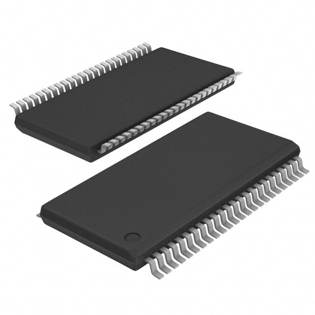
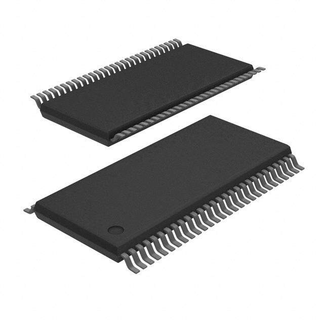
| 产品图片 |
|
| rohs | 符合RoHS无铅 / 符合限制有害物质指令(RoHS)规范要求 |
| 产品系列 | 逻辑集成电路,总线收发器,Texas Instruments SN74LVTH16245ADGVR74LVTH |
| 数据手册 | |
| 产品型号 | SN74LVTH16245ADGVR |
| 产品目录页面 | |
| 产品种类 | 总线收发器 |
| 传播延迟时间 | 4.1 ns |
| 低电平输出电流 | 64 mA |
| 供应商器件封装 | 48-TVSOP |
| 元件数 | 2 |
| 其它名称 | 296-8679-1 |
| 功能 | Bus Transceiver |
| 包装 | 剪切带 (CT) |
| 单位重量 | 123.500 mg |
| 商标 | Texas Instruments |
| 安装类型 | 表面贴装 |
| 安装风格 | SMD/SMT |
| 封装 | Reel |
| 封装/外壳 | 48-TFSOP(0.173",4.40mm 宽) |
| 封装/箱体 | TVSOP-48 |
| 工作温度 | -40°C ~ 85°C |
| 工厂包装数量 | 2000 |
| 最大工作温度 | + 85 C |
| 最小工作温度 | - 40 C |
| 极性 | Non-Inverting |
| 标准包装 | 1 |
| 每元件位数 | 8 |
| 每芯片的通道数量 | 16 |
| 电压-电源 | 2.7 V ~ 3.6 V |
| 电流-输出高,低 | 32mA,64mA |
| 电源电压-最大 | 3.6 V |
| 电源电压-最小 | 2.7 V |
| 电路数量 | 2 |
| 系列 | SN74LVTH16245A |
| 输入电平 | TTL/CMOS |
| 输出电平 | LVTTL |
| 输出类型 | 3-State |
| 逻辑类型 | 收发器,非反相 |
| 逻辑系列 | LVT |
| 高电平输出电流 | - 32 mA |


- 商务部:美国ITC正式对集成电路等产品启动337调查
- 曝三星4nm工艺存在良率问题 高通将骁龙8 Gen1或转产台积电
- 太阳诱电将投资9.5亿元在常州建新厂生产MLCC 预计2023年完工
- 英特尔发布欧洲新工厂建设计划 深化IDM 2.0 战略
- 台积电先进制程称霸业界 有大客户加持明年业绩稳了
- 达到5530亿美元!SIA预计今年全球半导体销售额将创下新高
- 英特尔拟将自动驾驶子公司Mobileye上市 估值或超500亿美元
- 三星加码芯片和SET,合并消费电子和移动部门,撤换高东真等 CEO
- 三星电子宣布重大人事变动 还合并消费电子和移动部门
- 海关总署:前11个月进口集成电路产品价值2.52万亿元 增长14.8%


PDF Datasheet 数据手册内容提取
SN54LVTH16245A,, SN74LVTH16245A 3.3-V ABT 16-BIT BUS TRANSCEIVERS WITH 3-STATE OUTPUTS www.ti.com SCBS143R–MAY1992–REVISEDNOVEMBER2006 FEATURES SN54LVTH16245A...WD PACKAGE • MembersoftheTexasInstrumentsWidebus™ SN74LVTH16245A...DGG, DGV, OR DL PACKAGE Family (TOP VIEW) • State-of-the-ArtAdvancedBiCMOS Technology(ABT)Designfor3.3-VOperation 1DIR 1 48 1OE andLowStatic-PowerDissipation 1B1 2 47 1A1 • SupportMixed-ModeSignalOperation(5-V 1B2 3 46 1A2 GND 4 45 GND InputandOutputVoltagesWith3.3-VV ) CC 1B3 5 44 1A3 • SupportUnregulatedBatteryOperationDown 1B4 6 43 1A4 to2.7V V 7 42 V • TypicalV (OutputGroundBounce)<0.8V CC CC OLP 1B5 8 41 1A5 atV =3.3V,T =25(cid:176) C CC A 1B6 9 40 1A6 • DistributedVCCandGNDPinsMinimize GND 10 39 GND High-SpeedSwitchingNoise 1B7 11 38 1A7 • Flow-ThroughArchitectureOptimizesPCB 1B8 12 37 1A8 Layout 2B1 13 36 2A1 • I andPower-Up3-StateSupportHot 2B2 14 35 2A2 off Insertion GND 15 34 GND • BusHoldonDataInputsEliminatestheNeed 2B3 16 33 2A3 2B4 17 32 2A4 forExternalPullup/PulldownResistors V 18 31 V • Latch-UpPerformanceExceeds500mAPer CC CC 2B5 19 30 2A5 JESD17 2B6 20 29 2A6 • ESDProtectionExceedsJESD22 GND 21 28 GND – 2000-VHuman-BodyModel(A114-A) 2B7 22 27 2A7 – 200-VMachineModel(A115-A) 2B8 23 26 2A8 2DIR 24 25 2OE DESCRIPTION/ORDERING INFORMATION The 'LVTH16245A devices are 16-bit (dual-octal) noninverting 3-state transceivers designed for low-voltage (3.3-V)V operation,butwiththecapabilitytoprovideaTTLinterfacetoa5-Vsystemenvironment. CC The devices are designed for asynchronous communication between two data buses. The logic levels of the direction-control (DIR) input and the output-enable (OE) input activate either the B-port outputs or the A-port outputs or place both output ports into the high-impedance mode. The device transmits data from the A bus to the B bus when the B-port outputs are activated, and from the B bus to the A bus when the A-port outputs are activated. The input circuitry on both A and B ports is always active and must have a logic HIGH or LOW level appliedtopreventexcessI andI . CC CCZ Active bus-hold circuitry holds unused or undriven inputs at a valid logic state. Use of pullup or pulldown resistorswiththebus-holdcircuitryisnotrecommended. When V is between 0 and 1.5 V, the devices are in the high-impedance state during power up or power down. CC However, to ensure the high-impedance state above 1.5 V, OE should be tied to V through a pullup resistor; CC theminimumvalueoftheresistorisdeterminedbythecurrent-sinkingcapabilityofthedriver. These devices are fully specified for hot-insertion applications using I and power-up 3-state. The I circuitry off off disables the outputs, preventing damaging current backflow through the devices when they are powered down. The power-up 3-state circuitry places the outputs in the high-impedance state during power up and power down, whichpreventsdriverconflict. Pleasebeawarethatanimportantnoticeconcerningavailability,standardwarranty,anduseincriticalapplicationsofTexas Instrumentssemiconductorproductsanddisclaimerstheretoappearsattheendofthisdatasheet. WidebusisatrademarkofTexasInstruments. PRODUCTIONDATAinformationiscurrentasofpublicationdate. Copyright©1992–2006,TexasInstrumentsIncorporated Products conform to specifications per the terms of the Texas On products compliant to MIL-PRF-38535, all parameters are Instruments standard warranty. Production processing does not testedunlessotherwisenoted.Onallotherproducts,production necessarilyincludetestingofallparameters. processingdoesnotnecessarilyincludetestingofallparameters.
SN54LVTH16245A,, SN74LVTH16245A 3.3-V ABT 16-BIT BUS TRANSCEIVERS WITH 3-STATE OUTPUTS www.ti.com SCBS143R–MAY1992–REVISEDNOVEMBER2006 ORDERINGINFORMATION T PACKAGE(1) ORDERABLEPARTNUMBER TOP-SIDEMARKING A FBGA–GRD SN74LVTH16245AGRDR Reelof1000 LL245A FBGA–ZRD(Pb-free) SN74LVTH16245AZRDR 74LVTH16245ADL Tubeof25 74LVTH16245ADLG4 SSOP–DL LVTH16245A 74LVTH16245ADLR Reelof1000 74LVTH16245ADLRG4 –40(cid:176) Cto85(cid:176) C SN74LVTH16245ADGGR TSSOP–DGG Reelof2000 74LVTH16245ADGGRE4 LVTH16245A 74LVTH16245ADGGRG4 SN74LVTH16245ADGVR TVSOP–DGV Reelof2000 LL245A 74LVTH16245ADGVRE4 VFBGA–GQL SN74LVTH16245AGQLR Reelof1000 LL245A VFBGA–ZQL(Pb-free) 74LVTH16245AZQLR –55(cid:176) Cto125(cid:176) C CFP–WD Tube SNJ54LVTH16245AWD SNJ54LVTH16245AWD (1) Packagedrawings,standardpackingquantities,thermaldata,symbolization,andPCBdesignguidelinesareavailableat www.ti.com/sc/package. GQL OR ZQL PACKAGE TERMINALASSIGNMENTS(1) (TOP VIEW) (56-BallGQL/ZQLPackage) 1 2 3 4 5 6 1 2 3 4 5 6 A A 1DIR NC NC NC NC 1OE B B 1B2 1B1 GND GND 1A1 1A2 C D C 1B4 1B3 V V 1A3 1A4 CC CC E D 1B6 1B5 GND GND 1A5 1A6 F E 1B8 1B7 1A7 1A8 G H F 2B1 2B2 2A2 2A1 J G 2B3 2B4 GND GND 2A4 2A3 K H 2B5 2B6 V V 2A6 2A5 CC CC J 2B7 2B8 GND GND 2A8 2A7 K 2DIR NC NC NC NC 2OE abc abc (1) NC–Nointernalconnection abc 2 SubmitDocumentationFeedback
SN54LVTH16245A,, SN74LVTH16245A 3.3-V ABT 16-BIT BUS TRANSCEIVERS WITH 3-STATE OUTPUTS www.ti.com SCBS143R–MAY1992–REVISEDNOVEMBER2006 GRD OR ZRD PACKAGE TERMINALASSIGNMENTS(1) (TOP VIEW) (54-BallGRD/ZRDPackage) 1 2 3 4 5 6 1 2 3 4 5 6 A 1B1 NC 1DIR 1OE NC 1A1 A B 1B3 1B2 NC NC 1A2 1A3 B C 1B5 1B4 V V 1A4 1A5 CC CC C D 1B7 1B6 GND GND 1A6 1A7 E 2B1 1B8 GND GND 1A8 2A1 D F 2B3 2B2 GND GND 2A2 2A3 E G 2B5 2B4 V V 2A4 2A5 CC CC F H 2B7 2B6 NC NC 2A6 2A7 G J 2B8 NC 2DIR 2OE NC 2A8 H J (1) NC–Nointernalconnection FUNCTIONTABLE(1) (EACH8-BITSECTION) CONTROL OUTPUTCIRCUITS INPUTS OPERATION OE DIR APORT BPORT L L Enabled Hi-Z BdatatoAbus L H Hi-Z Enabled AdatatoBbus H X Hi-Z Hi-Z Isolation (1) InputcircuitsofthedataI/Osalwaysareactive. LOGICDIAGRAM(POSITIVELOGIC) 1 24 1DIR 2DIR 48 25 1OE 2OE 47 36 1A1 2A1 2 13 1B1 2B1 To Seven Other Channels To Seven Other Channels SubmitDocumentationFeedback 3
SN54LVTH16245A,, SN74LVTH16245A 3.3-V ABT 16-BIT BUS TRANSCEIVERS WITH 3-STATE OUTPUTS www.ti.com SCBS143R–MAY1992–REVISEDNOVEMBER2006 Absolute Maximum Ratings(1) overoperatingfree-airtemperaturerange(unlessotherwisenoted) MIN MAX UNIT V Supplyvoltagerange –0.5 4.6 V CC V Inputvoltagerange(2) –0.5 7 V I V Voltagerangeappliedtoanyoutputinthehigh-impedanceorpower-offstate(2) –0.5 7 V O V Voltagerangeappliedtoanyoutputinthehighstate(2) –0.5 V +0.5 V O CC SN54LVTH16245A 96 I Currentintoanyoutputinthelowstate mA O SN74LVTH16245A 128 SN54LVTH16245A 48 I Currentintoanyoutputinthehighstate(3) mA O SN74LVTH16245A 64 I Inputclampcurrent V <0 –50 mA IK I I Outputclampcurrent V <0 –50 mA OK O DGGpackage 70 DGVpackage 58 q Packagethermalimpedance(4) DLpackage 63 (cid:176) C/W JA GQL/ZQLpackage 42 GRD/ZRDpackage 36 T Storagetemperaturerange –65 150 (cid:176) C stg (1) Stressesbeyondthoselistedunder"absolutemaximumratings"maycausepermanentdamagetothedevice.Thesearestressratings only,andfunctionaloperationofthedeviceattheseoranyotherconditionsbeyondthoseindicatedunder"recommendedoperating conditions"isnotimplied.Exposuretoabsolute-maximum-ratedconditionsforextendedperiodsmayaffectdevicereliability. (2) Theinputandoutputnegative-voltageratingsmaybeexceedediftheinputandoutputclamp-currentratingsareobserved. (3) ThiscurrentflowsonlywhentheoutputisinthehighstateandV >V . O CC (4) ThepackagethermalimpedanceiscalculatedinaccordancewithJESD51-7. Recommended Operating Conditions(1) SN54LVTH16245A SN74LVTH16245A UNIT MIN MAX MIN MAX V Supplyvoltage 2.7 3.6 2.7 3.6 V CC V High-levelinputvoltage 2 2 V IH V Low-levelinputvoltage 0.8 0.8 V IL V Inputvoltage 5.5 5.5 V I I High-leveloutputcurrent –24 –32 mA OH I Low-leveloutputcurrent 48 64 mA OL D t/D v Inputtransitionriseorfallrate Outputsenabled 10 10 ns/V D t/D V Power-upramprate 200 200 m s/V CC T Operatingfree-airtemperature –55 125 –40 85 (cid:176) C A (1) AllunusedcontrolinputsofthedevicemustbeheldatV orGNDtoensureproperdeviceoperation.RefertotheTIapplicationreport, CC ImplicationsofSloworFloatingCMOSInputs,literaturenumberSCBA004. 4 SubmitDocumentationFeedback
SN54LVTH16245A,, SN74LVTH16245A 3.3-V ABT 16-BIT BUS TRANSCEIVERS WITH 3-STATE OUTPUTS www.ti.com SCBS143R–MAY1992–REVISEDNOVEMBER2006 Electrical Characteristics overrecommendedoperatingfree-airtemperaturerange(unlessotherwisenoted) SN54LVTH16245A SN74LVTH16245A PARAMETER TESTCONDITIONS UNIT MIN TYP(1) MAX MIN TYP(1) MAX V V =2.7V, I =–18mA –1.2 –1.2 V IK CC I V =2.7Vto3.6V, I =–100m A V –0.2 V –0.2 CC OH CC CC V =2.7V, I =–8mA 2.4 2.4 CC OH V V OH I =–24mA 2 OH V =3V CC I =–32mA 2 OH I =100m A 0.2 0.2 OL V =2.7V CC I =24mA 0.5 0.5 OL I =16mA 0.4 0.4 OL V V OL I =32mA 0.5 0.5 OL V =3V CC I =48mA 0.55 OL I =64mA 0.55 OL Control VCC=3.6V, VI=VCCorGND – 1 – 1 inputs V =0or3.6V, V =5.5V 10 10 CC I I V =5.5V 20 20 m A I I AorB V =3.6V V =V 5 5 port(2) CC I CC V =0 –5 –5 I I V =0, V orV =0to4.5V – 100 m A off CC I O V =0.8V 75 75 I V =3V CC I AorB VI=2V –75 –75 m A I(hold) port 500 V =3.6V,(3) V =0to3.6V CC I –750 I VCC=0to1.5V,VO=0.5Vto3V, – 100(4) – 100 m A OZPU OE=don'tcare I VCC=1.5Vto0,VO=0.5Vto3V, – 100(4) – 100 m A OZPD OE=don'tcare Outputshigh 0.19 0.19 V =3.6V, CC I I =0, Outputslow 5 5 mA CC O V =V orGND I CC Outputsdisabled 0.19 0.19 D I (5) VCC=3Vto3.6V,OneinputatVCC–0.6V, 0.2 0.2 mA CC OtherinputsatV orGND CC C V =3Vor0 4 4 pF i I C V =3Vor0 10 10 pF io O (1) AlltypicalvaluesareatV =3.3V,T =25(cid:176) C. CC A (2) UnusedpinsatV orGND CC (3) Thisisthebus-holdmaximumdynamiccurrent.Itistheminimumoverdrivecurrentrequiredtoswitchtheinputfromonestateto another. (4) OnproductscomplianttoMIL-PRF-38535,thisparameterisnotproductiontested. (5) ThisistheincreaseinsupplycurrentforeachinputthatisatthespecifiedTTLvoltagelevel,ratherthanV orGND. CC SubmitDocumentationFeedback 5
SN54LVTH16245A,, SN74LVTH16245A 3.3-V ABT 16-BIT BUS TRANSCEIVERS WITH 3-STATE OUTPUTS www.ti.com SCBS143R–MAY1992–REVISEDNOVEMBER2006 Switching Characteristics overrecommendedoperatingfree-airtemperaturerange,C =50pF(unlessotherwisenoted)(seeFigure1) L SN54LVTH16245A SN74LVTH16245A FROM TO V =3.3V V =3.3V PARAMETER (INPUT) (OUTPUT) C–C0.3V VCC=2.7V C–C0.3V VCC=2.7V UNIT MIN MAX MIN MAX MIN TYP(1) MAX MIN MAX t 0.5 4.5 4.6 1.5 2.3 3.3 3.7 PLH AorB BorA ns t 0.5 4.4 3.9 1.3 2.1 3.3 3.5 PHL t 0.5 6.5 6.6 1.5 2.8 4.5 5.3 PZH OE AorB ns t 0.5 5.4 6.2 1.6 2.9 4.6 5.2 PZL t 1 6.8 7 2.3 3.7 5.1 5.5 PHZ OE AorB ns t 1 6.2 6.3 2.2 3.5 5.1 5.4 PLZ t 0.5 0.5 sk(LH) ns t 0.5 0.5 sk(HL) (1) AlltypicalvaluesareatV =3.3V,T =25(cid:176) C. CC A 6 SubmitDocumentationFeedback
SN54LVTH16245A,, SN74LVTH16245A 3.3-V ABT 16-BIT BUS TRANSCEIVERS WITH 3-STATE OUTPUTS www.ti.com SCBS143R–MAY1992–REVISEDNOVEMBER2006 PARAMETER MEASUREMENT INFORMATION 6 V 500 W S1 Open TEST S1 From Output Under Test GND tPLH/tPHL Open tPLZ/tPZL 6 V (seCeL N= o5t0e pAF) 500 W tPHZ/tPZH GND 2.7 V LOAD CIRCUIT Timing Input 1.5 V 0 V tw tsu th 2.7 V 2.7 V Input 1.5 V 1.5 V Data Input 1.5 V 1.5 V 0 V 0 V VOLTAGE WAVEFORMS VOLTAGE WAVEFORMS PULSE DURATION SETUP AND HOLD TIMES 2.7 V 2.7 V Output Input 1.5 V 1.5 V 1.5 V 1.5 V Control 0 V 0 V tPLH tPHL tPZL tPLZ Output VOH Waveform 1 3 V Output 1.5 V 1.5 V 1.5 V S1 at 6 V VOL + 0.3 V VOL (see Note B) VOL tPHL tPLH tPZH tPHZ Output VOH Waveform 2 VOH Output 1.5 V 1.5 V S1 at GND 1.5 V VOH − 0.3 V VOL (see Note B) ≈0 V VOLTAGE WAVEFORMS VOLTAGE WAVEFORMS PROPAGATION DELAY TIMES ENABLE AND DISABLE TIMES INVERTING AND NONINVERTING OUTPUTS LOW- AND HIGH-LEVEL ENABLING NOTES: A. CL includes probe and jig capacitance. B. Waveform 1 is for an output with internal conditions such that the output is low, except when disabled by the output control. Waveform 2 is for an output with internal conditions such that the output is high, except when disabled by the output control. C. All input pulses are supplied by generators having the following characteristics: PRR ≤ 10 MHz, ZO = 50 W , tr ≤ 2.5 ns, tf ≤ 2.5 ns. D. The outputs are measured one at a time, with one transition per measurement. Figure1.LoadCircuitandVoltageWaveforms SubmitDocumentationFeedback 7
PACKAGE OPTION ADDENDUM www.ti.com 6-Feb-2020 PACKAGING INFORMATION Orderable Device Status Package Type Package Pins Package Eco Plan Lead/Ball Finish MSL Peak Temp Op Temp (°C) Device Marking Samples (1) Drawing Qty (2) (6) (3) (4/5) 5962-9668601QXA ACTIVE CFP WD 48 1 TBD Call TI N / A for Pkg Type -55 to 125 5962-9668601QX A SNJ54LVTH16245 AWD 5962-9668601VXA ACTIVE CFP WD 48 1 TBD Call TI N / A for Pkg Type -55 to 125 5962-9668601VX A SNV54LVTH16245 AWD 74LVTH16245ADGGRE4 ACTIVE TSSOP DGG 48 2000 Green (RoHS NIPDAU Level-1-260C-UNLIM -40 to 85 LVTH16245A & no Sb/Br) 74LVTH16245ADGGRG4 ACTIVE TSSOP DGG 48 2000 Green (RoHS NIPDAU Level-1-260C-UNLIM -40 to 85 LVTH16245A & no Sb/Br) 74LVTH16245ADGVRG4 ACTIVE TVSOP DGV 48 2000 Green (RoHS NIPDAU Level-1-260C-UNLIM -40 to 85 LL245A & no Sb/Br) 74LVTH16245ADLG4 ACTIVE SSOP DL 48 25 Green (RoHS NIPDAU Level-1-260C-UNLIM -40 to 85 LVTH16245A & no Sb/Br) 74LVTH16245ADLRG4 ACTIVE SSOP DL 48 1000 Green (RoHS NIPDAU Level-1-260C-UNLIM -40 to 85 LVTH16245A & no Sb/Br) SN74LVTH16245ADGGR ACTIVE TSSOP DGG 48 2000 Green (RoHS NIPDAU Level-1-260C-UNLIM -40 to 85 LVTH16245A & no Sb/Br) SN74LVTH16245ADGVR ACTIVE TVSOP DGV 48 2000 Green (RoHS NIPDAU Level-1-260C-UNLIM -40 to 85 LL245A & no Sb/Br) SN74LVTH16245ADL ACTIVE SSOP DL 48 25 Green (RoHS NIPDAU Level-1-260C-UNLIM -40 to 85 LVTH16245A & no Sb/Br) SN74LVTH16245ADLR ACTIVE SSOP DL 48 1000 Green (RoHS NIPDAU Level-1-260C-UNLIM -40 to 85 LVTH16245A & no Sb/Br) SN74LVTH16245AZQLR LIFEBUY BGA ZQL 56 1000 Green (RoHS SNAGCU Level-1-260C-UNLIM -40 to 85 LL245A MICROSTAR & no Sb/Br) JUNIOR SN74LVTH16245AZRDR LIFEBUY BGA ZRD 54 1000 Green (RoHS SNAGCU Level-1-260C-UNLIM -40 to 85 LL245A MICROSTAR & no Sb/Br) JUNIOR SNJ54LVTH16245AWD ACTIVE CFP WD 48 1 TBD Call TI N / A for Pkg Type -55 to 125 5962-9668601QX A SNJ54LVTH16245 Addendum-Page 1
PACKAGE OPTION ADDENDUM www.ti.com 6-Feb-2020 Orderable Device Status Package Type Package Pins Package Eco Plan Lead/Ball Finish MSL Peak Temp Op Temp (°C) Device Marking Samples (1) Drawing Qty (2) (6) (3) (4/5) AWD (1) The marketing status values are defined as follows: ACTIVE: Product device recommended for new designs. LIFEBUY: TI has announced that the device will be discontinued, and a lifetime-buy period is in effect. NRND: Not recommended for new designs. Device is in production to support existing customers, but TI does not recommend using this part in a new design. PREVIEW: Device has been announced but is not in production. Samples may or may not be available. OBSOLETE: TI has discontinued the production of the device. (2) RoHS: TI defines "RoHS" to mean semiconductor products that are compliant with the current EU RoHS requirements for all 10 RoHS substances, including the requirement that RoHS substance do not exceed 0.1% by weight in homogeneous materials. Where designed to be soldered at high temperatures, "RoHS" products are suitable for use in specified lead-free processes. TI may reference these types of products as "Pb-Free". RoHS Exempt: TI defines "RoHS Exempt" to mean products that contain lead but are compliant with EU RoHS pursuant to a specific EU RoHS exemption. Green: TI defines "Green" to mean the content of Chlorine (Cl) and Bromine (Br) based flame retardants meet JS709B low halogen requirements of <=1000ppm threshold. Antimony trioxide based flame retardants must also meet the <=1000ppm threshold requirement. (3) MSL, Peak Temp. - The Moisture Sensitivity Level rating according to the JEDEC industry standard classifications, and peak solder temperature. (4) There may be additional marking, which relates to the logo, the lot trace code information, or the environmental category on the device. (5) Multiple Device Markings will be inside parentheses. Only one Device Marking contained in parentheses and separated by a "~" will appear on a device. If a line is indented then it is a continuation of the previous line and the two combined represent the entire Device Marking for that device. (6) Lead/Ball Finish - Orderable Devices may have multiple material finish options. Finish options are separated by a vertical ruled line. Lead/Ball Finish values may wrap to two lines if the finish value exceeds the maximum column width. Important Information and Disclaimer:The information provided on this page represents TI's knowledge and belief as of the date that it is provided. TI bases its knowledge and belief on information provided by third parties, and makes no representation or warranty as to the accuracy of such information. Efforts are underway to better integrate information from third parties. TI has taken and continues to take reasonable steps to provide representative and accurate information but may not have conducted destructive testing or chemical analysis on incoming materials and chemicals. TI and TI suppliers consider certain information to be proprietary, and thus CAS numbers and other limited information may not be available for release. In no event shall TI's liability arising out of such information exceed the total purchase price of the TI part(s) at issue in this document sold by TI to Customer on an annual basis. OTHER QUALIFIED VERSIONS OF SN54LVTH16245A, SN54LVTH16245A-SP, SN74LVTH16245A : •Catalog: SN74LVTH16245A, SN54LVTH16245A Addendum-Page 2
PACKAGE OPTION ADDENDUM www.ti.com 6-Feb-2020 •Automotive: SN74LVTH16245A-Q1, SN74LVTH16245A-Q1 •Enhanced Product: SN74LVTH16245A-EP, SN74LVTH16245A-EP •Military: SN54LVTH16245A •Space: SN54LVTH16245A-SP NOTE: Qualified Version Definitions: •Catalog - TI's standard catalog product •Automotive - Q100 devices qualified for high-reliability automotive applications targeting zero defects •Enhanced Product - Supports Defense, Aerospace and Medical Applications •Military - QML certified for Military and Defense Applications •Space - Radiation tolerant, ceramic packaging and qualified for use in Space-based application Addendum-Page 3
PACKAGE MATERIALS INFORMATION www.ti.com 12-Feb-2019 TAPE AND REEL INFORMATION *Alldimensionsarenominal Device Package Package Pins SPQ Reel Reel A0 B0 K0 P1 W Pin1 Type Drawing Diameter Width (mm) (mm) (mm) (mm) (mm) Quadrant (mm) W1(mm) SN74LVTH16245ADGGR TSSOP DGG 48 2000 330.0 24.4 8.6 13.0 1.8 12.0 24.0 Q1 SN74LVTH16245ADGVR TVSOP DGV 48 2000 330.0 16.4 7.1 10.2 1.6 12.0 16.0 Q1 SN74LVTH16245ADLR SSOP DL 48 1000 330.0 32.4 11.35 16.2 3.1 16.0 32.0 Q1 SN74LVTH16245AZQLR BGAMI ZQL 56 1000 330.0 16.4 4.8 7.3 1.5 8.0 16.0 Q1 CROSTA RJUNI OR SN74LVTH16245AZRDR BGAMI ZRD 54 1000 330.0 16.4 5.8 8.3 1.55 8.0 16.0 Q1 CROSTA RJUNI OR PackMaterials-Page1
PACKAGE MATERIALS INFORMATION www.ti.com 12-Feb-2019 *Alldimensionsarenominal Device PackageType PackageDrawing Pins SPQ Length(mm) Width(mm) Height(mm) SN74LVTH16245ADGGR TSSOP DGG 48 2000 367.0 367.0 45.0 SN74LVTH16245ADGVR TVSOP DGV 48 2000 367.0 367.0 38.0 SN74LVTH16245ADLR SSOP DL 48 1000 367.0 367.0 55.0 SN74LVTH16245AZQLR BGAMICROSTAR ZQL 56 1000 350.0 350.0 43.0 JUNIOR SN74LVTH16245AZRDR BGAMICROSTAR ZRD 54 1000 350.0 350.0 43.0 JUNIOR PackMaterials-Page2
None
MECHANICAL DATA MPDS006C – FEBRUARY 1996 – REVISED AUGUST 2000 DGV (R-PDSO-G**) PLASTIC SMALL-OUTLINE 24 PINS SHOWN 0,23 0,40 0,07 M 0,13 24 13 0,16 NOM 4,50 6,60 4,30 6,20 Gage Plane 0,25 0°–(cid:1)8° 0,75 1 12 0,50 A Seating Plane 0,15 1,20 MAX 0,08 0,05 PINS ** 14 16 20 24 38 48 56 DIM A MAX 3,70 3,70 5,10 5,10 7,90 9,80 11,40 A MIN 3,50 3,50 4,90 4,90 7,70 9,60 11,20 4073251/E 08/00 NOTES: A. All linear dimensions are in millimeters. B. This drawing is subject to change without notice. C. Body dimensions do not include mold flash or protrusion, not to exceed 0,15 per side. D. Falls within JEDEC: 24/48 Pins – MO-153 14/16/20/56 Pins – MO-194 • POST OFFICE BOX 655303 DALLAS, TEXAS 75265
MECHANICAL DATA MTSS003D – JANUARY 1995 – REVISED JANUARY 1998 DGG (R-PDSO-G**) PLASTIC SMALL-OUTLINE PACKAGE 48 PINS SHOWN 0,27 0,50 0,08 M 0,17 48 25 6,20 8,30 6,00 7,90 0,15 NOM Gage Plane 0,25 1 24 0°–8° A 0,75 0,50 Seating Plane 0,15 1,20 MAX 0,10 0,05 PINS ** 48 56 64 DIM A MAX 12,60 14,10 17,10 A MIN 12,40 13,90 16,90 4040078/F 12/97 NOTES: A. All linear dimensions are in millimeters. B. This drawing is subject to change without notice. C. Body dimensions do not include mold protrusion not to exceed 0,15. D. Falls within JEDEC MO-153 • POST OFFICE BOX 655303 DALLAS, TEXAS 75265
PACKAGE OUTLINE ZQL0056A JRBGA - 1 mm max height SCALE 2.100 PLASTIC BALL GRID ARRAY 4.6 B A 4.4 BALL A1 CORNER 7.1 6.9 1 MAX C SEATING PLANE 0.35 0.15 TYP BALL TYP 0.1 C 3.25 TYP SYMM (0.625) TYP K J (0.575) TYP H G 5.85 F SYMM TYP E D C 0.45 56X NOTE 3 0.35 B 0.15 C B A 0.08 C A 0.65 TYP 1 2 3 4 5 6 BALL A1 CORNER 0.65 TYP 4219711/B 01/2017 NOTES: 1. All linear dimensions are in millimeters. Any dimensions in parenthesis are for reference only. Dimensioning and tolerancing per ASME Y14.5M. 2. This drawing is subject to change without notice. 3. No metal in this area, indicates orientation. www.ti.com
EXAMPLE BOARD LAYOUT ZQL0056A JRBGA - 1 mm max height PLASTIC BALL GRID ARRAY (0.65) TYP 56X ( 0.33) 1 2 3 4 5 6 A (0.65) TYP B C D E SYMM F G H J K SYMM LAND PATTERN EXAMPLE EXPOSED METAL SHOWN SCALE:15X SOLDER MASK 0.05 MAX 0.05 MIN METAL UNDER OPENING SOLDER MASK EXPOSED METAL ( 0.33) ( 0.33) METAL EXPOSED METAL SOLDER MASK OPENING NON-SOLDER MASK SOLDER MASK DEFINED DEFINED (PREFERRED) SOLDER MASK DETAILS NOT TO SCALE 4219711/B 01/2017 NOTES: (continued) 4. Final dimensions may vary due to manufacturing tolerance considerations and also routing constraints. For information, see Texas Instruments literature number SPRAA99 (www.ti.com/lit/spraa99). www.ti.com
EXAMPLE STENCIL DESIGN ZQL0056A JRBGA - 1 mm max height PLASTIC BALL GRID ARRAY 56X ( 0.33) (0.65) TYP 1 2 3 4 5 6 A (0.65) TYP B C D E SYMM F G H J K SYMM SOLDER PASTE EXAMPLE BASED ON 0.125 mm THICK STENCIL SCALE:15X 4219711/B 01/2017 NOTES: (continued) 5. Laser cutting apertures with trapezoidal walls and rounded corners may offer better paste release. www.ti.com
MECHANICAL DATA MCFP010B – JANUARY 1995 – REVISED NOVEMBER 1997 WD (R-GDFP-F**) CERAMIC DUAL FLATPACK 48 LEADS SHOWN 0.120 (3,05) 0.009 (0,23) 0.075 (1,91) 0.004 (0,10) 1.130 (28,70) 0.870 (22,10) 0.370 (9,40) 0.390 (9,91) 0.370 (9,40) 0.250 (6,35) 0.370 (9,40) 0.250 (6,35) 1 48 0.025 (0,635) A 0.014 (0,36) 0.008 (0,20) 24 25 NO. OF 48 56 LEADS** 0.640 0.740 A MAX (16,26) (18,80) 0.610 0.710 A MIN (15,49) (18,03) 4040176/D 10/97 NOTES: A. All linear dimensions are in inches (millimeters). B. This drawing is subject to change without notice. C. This package can be hermetically sealed with a ceramic lid using glass frit. D. Index point is provided on cap for terminal identification only E. Falls within MIL STD 1835: GDFP1-F48 and JEDEC MO-146AA GDFP1-F56 and JEDEC MO-146AB • POST OFFICE BOX 655303 DALLAS, TEXAS 75265
None
IMPORTANTNOTICEANDDISCLAIMER TI PROVIDES TECHNICAL AND RELIABILITY DATA (INCLUDING DATASHEETS), DESIGN RESOURCES (INCLUDING REFERENCE DESIGNS), APPLICATION OR OTHER DESIGN ADVICE, WEB TOOLS, SAFETY INFORMATION, AND OTHER RESOURCES “AS IS” AND WITH ALL FAULTS, AND DISCLAIMS ALL WARRANTIES, EXPRESS AND IMPLIED, INCLUDING WITHOUT LIMITATION ANY IMPLIED WARRANTIES OF MERCHANTABILITY, FITNESS FOR A PARTICULAR PURPOSE OR NON-INFRINGEMENT OF THIRD PARTY INTELLECTUAL PROPERTY RIGHTS. These resources are intended for skilled developers designing with TI products. You are solely responsible for (1) selecting the appropriate TI products for your application, (2) designing, validating and testing your application, and (3) ensuring your application meets applicable standards, and any other safety, security, or other requirements. These resources are subject to change without notice. TI grants you permission to use these resources only for development of an application that uses the TI products described in the resource. Other reproduction and display of these resources is prohibited. No license is granted to any other TI intellectual property right or to any third party intellectual property right. TI disclaims responsibility for, and you will fully indemnify TI and its representatives against, any claims, damages, costs, losses, and liabilities arising out of your use of these resources. TI’s products are provided subject to TI’s Terms of Sale (www.ti.com/legal/termsofsale.html) or other applicable terms available either on ti.com or provided in conjunction with such TI products. TI’s provision of these resources does not expand or otherwise alter TI’s applicable warranties or warranty disclaimers for TI products. Mailing Address: Texas Instruments, Post Office Box 655303, Dallas, Texas 75265 Copyright © 2020, Texas Instruments Incorporated