ICGOO在线商城 > 集成电路(IC) > 逻辑 - 缓冲器,驱动器,接收器,收发器 > 74LVT162245MTD

 Datasheet下载
- 型号: 74LVT162245MTD
- 制造商: Fairchild Semiconductor
- 库位|库存: xxxx|xxxx
- 要求:
| 数量阶梯 | 香港交货 | 国内含税 |
| +xxxx | $xxxx | ¥xxxx |
查看当月历史价格
查看今年历史价格
74LVT162245MTD产品简介:
ICGOO电子元器件商城为您提供74LVT162245MTD由Fairchild Semiconductor设计生产,在icgoo商城现货销售,并且可以通过原厂、代理商等渠道进行代购。 74LVT162245MTD价格参考¥7.73-¥14.29。Fairchild Semiconductor74LVT162245MTD封装/规格:逻辑 - 缓冲器,驱动器,接收器,收发器, Transceiver, Non-Inverting 2 Element 8 Bit per Element 3-State Output 48-TSSOP。您可以下载74LVT162245MTD参考资料、Datasheet数据手册功能说明书,资料中有74LVT162245MTD 详细功能的应用电路图电压和使用方法及教程。
ON Semiconductor的74LVT162245MTD是一款逻辑缓冲器/驱动器/接收器/收发器,广泛应用于需要高速数据传输和信号转换的场景。以下是其主要应用场景:

1. 计算机外设:该芯片适用于计算机外设设备,如打印机、扫描仪和存储设备等,提供高效的数据传输和信号处理能力。

2. 通信系统:在通信设备中,74LVT162245MTD可以用于信号放大和数据转发,支持多路信号的同时传输,确保数据的完整性和稳定性。

3. 工业自动化:在工业控制领域,这款芯片可用于数据采集系统、可编程逻辑控制器(PLC)和其他自动化设备中,实现信号的可靠传输和转换。

4. 消费电子:包括电视、音响系统和其他多媒体设备在内的消费电子产品中,该芯片能够处理音频和视频信号的传输与转换,提升用户体验。

5. 网络设备:在网络交换机、路由器等设备中,74LVT162245MTD可以作为信号中继器,增强信号强度并扩展传输距离。

6. 汽车电子:在现代汽车中,这款芯片可用于车载信息娱乐系统、导航系统以及传感器数据处理,确保车内电子系统的高效运行。

总之,74LVT162245MTD凭借其高性能和可靠性,适合各种需要快速、稳定信号传输的应用场合。
| 参数 | 数值 |
| 产品目录 | 集成电路 (IC)半导体 |
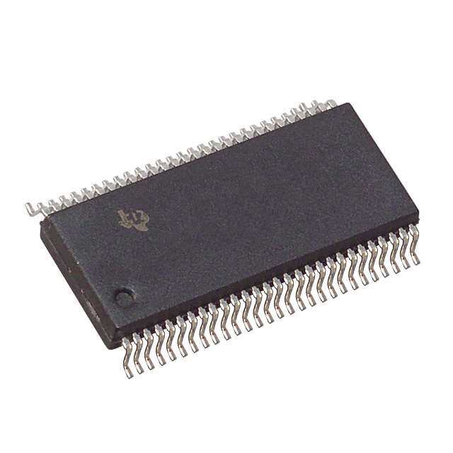
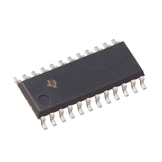
| 描述 | IC TRANSCVR TRI-ST 16BIT 48TSSOP总线收发器 16-Bit Transceiver |
| 产品分类 | |
| 品牌 | Fairchild Semiconductor |
| 产品手册 | |
| 产品图片 |
|
| rohs | 符合RoHS无铅 / 符合限制有害物质指令(RoHS)规范要求 |
| 产品系列 | 逻辑集成电路,总线收发器,Fairchild Semiconductor 74LVT162245MTD74LVT |
| 数据手册 | |
| 产品型号 | 74LVT162245MTD |
| 产品种类 | 总线收发器 |
| 传播延迟时间 | 4.6 ns |
| 低电平输出电流 | 64 mA |
| 供应商器件封装 | 48-TSSOP |
| 元件数 | 2 |
| 功能 | Transceiver |
| 包装 | 管件 |
| 单位重量 | 421 mg |
| 商标 | Fairchild Semiconductor |
| 安装类型 | 表面贴装 |
| 安装风格 | SMD/SMT |
| 封装 | Tube |
| 封装/外壳 | 48-TFSOP(0.240",6.10mm 宽) |
| 封装/箱体 | TSSOP-48 |
| 工作温度 | -40°C ~ 85°C |
| 工厂包装数量 | 38 |
| 最大工作温度 | + 85 C |
| 最小工作温度 | - 40 C |
| 极性 | Non-Inverting |
| 标准包装 | 38 |
| 每元件位数 | 8 |
| 每芯片的通道数量 | 16 |
| 电压-电源 | 2.7 V ~ 3.6 V |
| 电流-输出高,低 | 12mA,12mA; 32mA,64mA |
| 电源电压-最大 | 3.6 V |
| 电源电压-最小 | 2.7 V |
| 电路数量 | 2 |
| 系列 | 74LVT162245 |
| 输入电平 | LVTTL |
| 输出电平 | LVTTL |
| 输出类型 | 3-State |
| 逻辑类型 | 收发器,非反相 |
| 逻辑系列 | 74LVT |
| 高电平输出电流 | - 32 mA |


- 商务部:美国ITC正式对集成电路等产品启动337调查
- 曝三星4nm工艺存在良率问题 高通将骁龙8 Gen1或转产台积电
- 太阳诱电将投资9.5亿元在常州建新厂生产MLCC 预计2023年完工
- 英特尔发布欧洲新工厂建设计划 深化IDM 2.0 战略
- 台积电先进制程称霸业界 有大客户加持明年业绩稳了
- 达到5530亿美元!SIA预计今年全球半导体销售额将创下新高
- 英特尔拟将自动驾驶子公司Mobileye上市 估值或超500亿美元
- 三星加码芯片和SET,合并消费电子和移动部门,撤换高东真等 CEO
- 三星电子宣布重大人事变动 还合并消费电子和移动部门
- 海关总署:前11个月进口集成电路产品价值2.52万亿元 增长14.8%


PDF Datasheet 数据手册内容提取
Is Now Part of To learn more about ON Semiconductor, please visit our website at www.onsemi.com Please note: As part of the Fairchild Semiconductor integration, some of the Fairchild orderable part numbers will need to change in order to meet ON Semiconductor’s system requirements. Since the ON Semiconductor product management systems do not have the ability to manage part nomenclature that utilizes an underscore (_), the underscore (_) in the Fairchild part numbers will be changed to a dash (-). This document may contain device numbers with an underscore (_). Please check the ON Semiconductor website to verify the updated device numbers. The most current and up-to-date ordering information can be found at www.onsemi.com. Please email any questions regarding the system integration to Fairchild_questions@onsemi.com. ON Semiconductor and the ON Semiconductor logo are trademarks of Semiconductor Components Industries, LLC dba ON Semiconductor or its subsidiaries in the United States and/or other countries. ON Semiconductor owns the rights to a number of patents, trademarks, copyrights, trade secrets, and other intellectual property. A listing of ON Semiconductor’s product/patent coverage may be accessed at www.onsemi.com/site/pdf/Patent-Marking.pdf. ON Semiconductor reserves the right to make changes without further notice to any products herein. ON Semiconductor makes no warranty, representation or guarantee regarding the suitability of its products for any particular purpose, nor does ON Semiconductor assume any liability arising out of the application or use of any product or circuit, and specifically disclaims any and all liability, including without limitation special, consequential or incidental damages. Buyer is responsible for its products and applications using ON Semiconductor products, including compliance with all laws, regulations and safety requirements or standards, regardless of any support or applications information provided by ON Semiconductor. “Typical” parameters which may be provided in ON Semiconductor data sheets and/or specifications can and do vary in different applications and actual performance may vary over time. All operating parameters, including “Typicals” must be validated for each customer application by customer’s technical experts. ON Semiconductor does not convey any license under its patent rights nor the rights of others. ON Semiconductor products are not designed, intended, or authorized for use as a critical component in life support systems or any FDA Class 3 medical devices or medical devices with a same or similar classification in a foreign jurisdiction or any devices intended for implantation in the human body. Should Buyer purchase or use ON Semiconductor products for any such unintended or unauthorized application, Buyer shall indemnify and hold ON Semiconductor and its officers, employees, subsidiaries, affiliates, and distributors harmless against all claims, costs, damages, and expenses, and reasonable attorney fees arising out of, directly or indirectly, any claim of personal injury or death associated with such unintended or unauthorized use, even if such claim alleges that ON Semiconductor was negligent regarding the design or manufacture of the part. ON Semiconductor is an Equal Opportunity/Affirmative Action Employer. This literature is subject to all applicable copyright laws and is not for resale in any manner.
A 7 January 1999 P 4L Revised June 2005 o V r T t 1 O 6 u 2 74LVT162245 (cid:127) 74LVTH162245 tp 24 u 5 Low Voltage 16-Bit Transceiver with 3-STATE Outputs ts • 7 and 25(cid:1) Series Resistors in A Port Outputs 4 L V T General Description Features H 1 The LVT162245 and LVTH162245 contains sixteen non- (cid:1) Input and output interface capability to systems at 6 2 inverting bidirectional buffers with 3-STATE outputs and is 5V VCC 2 intended for bus oriented applications. The device is byte (cid:1) Bushold data inputs eliminate the need for external pull- 4 controlled. Each byte has separate control inputs which 5 can be shorted together for full 16-bit operation. The T/R up resistors to hold unused inputs (74LVTH162245), L also available without bushold feature (74LVT162245). o inputs determine the direction of data flow through the (cid:1) Live insertion/extraction permitted w device. The OE inputs disable both the A and B ports by placing them in a high impedance state. (cid:1) Power Up/Down high impedance provides glitch-free V o bus loading The LVT162245 and LVTH162245 are designed with l equivalent 25: series resistance in both the HIGH and (cid:1) A Port outputs include equivalent series resistance of ta LOW states on the A Port outputs. This design reduces line 25: making external termination resistors unnecessary ge noise in applications such as memory address drivers, and reducing overshoot and undershoot 1 clock drivers, and bus transceivers/transmitters. (cid:1) A Port outputs source/sink r12 mA. 6 The LVTH162245 data inputs include bushold, eliminating B Port outputs source/sink (cid:16)32 mA/(cid:14)64 mA -B the need for external pull-up resistors to hold unused (cid:1) Functionally compatible with the 74 series 162245 it inputs. (cid:1) Latch-up performance exceeds 500 mA T r These non-inverting transceivers are designed for low volt- (cid:1) ESD performance: a age (3.3V) VCC applications, but with the capability to pro- Human-body model ! 2000V ns vide a TTL interface to a 5V environment. The LVT162245 c and LVTH162245 are fabricated with an advanced Machine model ! 200V e BiCMOS technology to achieve high speed operation simi- Charged-device model ! 1000V iv lar to 5V ABT while maintaining a low power dissipation. (cid:1) Also packaged in plastic Fine Pitch Ball Grid Array er (FBGA) w it h Ordering Code: 3 - S T Order Number Package Number Package Description A 74LVT162245G BGA54A 54-Ball Fine-Pitch Ball Grid Array (FBGA), JEDEC MO-205, 5.5mm Wide T E (Note 1)(Note 2) (Preliminary) O 74LVT162245MEA MS48A 48-Lead Small Shrink Outline Package (SSOP), JEDEC MO-118, 0.300" Wide u (Note 2) t p 74LVT162245MTD MTD48 48-Lead Thin Shrink Small Outline Package (TSSOP), JEDEC MO-153, 6.1mm Wide u (Note 2) t s 74LVTH162245G BGA54A 54-Ball Fine-Pitch Ball Grid Array (FBGA), JEDEC MO-205, 5.5mm Wide a (Note 1)(Note 2) n d 74LVTH162245MEA MS48A 48-Lead Small Shrink Outline Package (SSOP), JEDEC MO-118, 0.300" Wide [TUBE] 2 5 74LVTH162245MEX MS48A 48-Lead Small Shrink Outline Package (SSOP), JEDEC MO-118, 0.300" Wide (cid:1) [TAPE and REEL] S 74LVTH162245MTD MTD48 48-Lead Thin Shrink Small Outline Package (TSSOP), JEDEC MO-153, 6.1mm Wide e [TUBE] rie 74LVTH162245MTX MTD48 48-Lead Thin Shrink Small Outline Package (TSSOP), JEDEC MO-153, 6.1mm Wide s [TAPE and REEL] R Note 1: Ordering code “G” indicates Trays. e s Note 2: Devices also available in Tape and Reel. Specify by appending the suffix letter “X” to the ordering code. is t o r s in © 2005 Fairchild Semiconductor Corporation DS012446 www.fairchildsemi.com
5 4 Logic Symbol 2 2 6 1 H T V L 4 7 (cid:127) 5 4 Connection Diagrams Pin Descriptions 2 2 6 Pin Assignments for SSOP and TSSOP Pin Names Description 1 VT OEn Output Enable Input (Active LOW) L T/Rn Transmit/Receive Input 74 A0–A15 Side A Inputs/3-STATE Outputs B0–B15 Side B Inputs/3-STATE Outputs NC No Connect FBGA Pin Assignments 1 2 3 4 5 6 A B0 NC T/R1 OE1 NC A0 B B2 B1 NC NC A1 A2 C B4 B3 VCC VCC A3 A4 D B6 B5 GND GND A5 A6 E B8 B7 GND GND A7 A8 F B10 B9 GND GND A9 A10 G B12 B11 VCC VCC A11 A12 H B14 B13 NC NC A13 A14 J B15 NC T/R2 OE2 NC A15 Truth Tables Inputs Outputs OE1 T/R1 Pin Assignment for FBGA L L Bus B0–B7 Data to Bus A0–A7 L H Bus A0–A7 Data to Bus B0–B7 H X HIGH-Z State on A0–A7, B0–B7 Inputs Outputs OE2 T/R2 L L Bus B8–B15 Data to Bus A8–A15 L H Bus A8–A15 Data to Bus B8–B15 H X HIGH-Z State on A8–A15, B8–B15 H HIGH Voltage Level L LOW Voltage Level X Immaterial Z High Impedance (Top Thru View) www.fairchildsemi.com 2
7 Functional Description 4 L V The LVT162245 and LVTH162245 contain sixteen non- cally, but independent of the other. The control pins can be T inverting bidirectional buffers with 3-STATE outputs. The shorted together to obtain full 16-bit operation. 1 device is byte controlled with each byte functioning identi- 6 2 2 Logic Diagrams 4 5 (cid:127) 7 4 L V T H 1 6 2 2 4 5 Please note that these diagrams are provided only for the understanding of logic operations and should not be used to estimate propagation delays. 3 www.fairchildsemi.com
5 4 Absolute Maximum Ratings 2 (Note 3) 2 6 Symbol Parameter Value Conditions Units 1 H VCC Supply Voltage (cid:16)0.5 to (cid:14)4.6 V VT VI DC Input Voltage (cid:16)0.5 to (cid:14)7.0 V 4L VO Output Voltage (cid:16)0.5 to (cid:14)7.0 Output in 3-STATE V 7 (cid:16)0.5 to (cid:14)7.0 Output in HIGH or LOW State (Note 4) (cid:127) IIK DC Input Diode Current (cid:16)50 VI (cid:31) GND mA 5 4 IOK DC Output Diode Current (cid:16)50 VO (cid:31) GND mA 22 IO DC Output Current 64 VO ! VCC Output at HIGH State mA 16 128 VO ! VCC Output at LOW State VT ICC DC Supply Current per Supply Pin r64 mA L IGND DC Ground Current per Ground Pin r128 mA 74 TSTG Storage Temperature (cid:16)65 to (cid:14)150 qC Recommended Operating Conditions Symbol Parameter Min Max Units VCC Supply Voltage 2.7 3.6 V VI Input Voltage 0 5.5 V IOH HIGH-Level Output Current B Port (cid:16)32 mA A Port (cid:16)12 IOL LOW-Level Output Current B Port 64 mA A Port 12 TA Free Air Operating Temperature (cid:16)40 (cid:14)85 qC ’t/’V Input Edge Rate, VIN 0.8V–2.0V, VCC 3.0V 0 10 ns/V Note 3: Absolute Maximum continuous ratings are those values beyond which damage to the device may occur. Exposure to these conditions or conditions beyond those indicated may adversely affect device reliability. Functional operation under absolute maximum rated conditions is not implied. Note 4: IO Absolute Maximum Rating must be observed. DC Electrical Characteristics VCC TA (cid:16)40qC to (cid:14)85qC Symbol Parameter Units Conditions (V) Min Max VIK Input Clamp Diode Voltage 2.7 (cid:16)1.2 V II (cid:16)18 mA VIH Input HIGH Voltage 2.7–3.6 2.0 V VO d 0.1V or VIL Input LOW Voltage 2.7–3.6 0.8 V VO t VCC (cid:16) 0.1V VOH OutputHIGHVoltage 3.0 2.0 V IOH (cid:16)12 mA A Port 2.7–3.6 VCC(cid:16)0.2 V IOH (cid:16)100 PA B Port 2.7 2.4 V IOH (cid:16)8 mA 3.0 2.0 IOH (cid:16)32 mA VOL Output LOW Voltage A Port 3.0 0.8 V IOL 12 mA 2.7 0.2 V IOL 100 PA 2.7 0.5 IOL 24 mA B Port 3.0 0.4 V IOL 16 mA 3.0 0.5 IOL 32 mA 3.0 0.55 IOL 64 mA II(HOLD) Bushold Input Minimum Drive 3.0 75 PA VI 0.8V (Note 5) (cid:16)75 VI 2.0V II(OD) Bushold Input Over-Drive 3.0 500 PA (Note 6) (Note 5) Current to Change State (cid:16)500 (Note 7) II Input Current 3.6 10 VI 5.5V Control Pins 3.6 r1 PA VI 0V or VCC Data Pins 3.6 (cid:16)5 VI 0V 1 VI VCC IOFF Power Off Leakage Current 0 r100 PA 0V d VI or VO d 5.5V www.fairchildsemi.com 4
7 DC Electrical Characteristics 4 (Continued) L V T Symbol Parameter VCC TA (cid:16)40qC to (cid:14)85qC Units Conditions 16 (V) Min Max 2 2 IPU/PD Power Up/Down 0–1.5V r100 PA VO 0.5V to 3.0V 4 3-STATE Current VI GND to VCC 5 IOZL 3-STATE Output Leakage Current 3.6 (cid:16)5 PA VO 0.5V (cid:127) 7 IOZL 3-STATE Output Leakage Current 3.6 (cid:16)5 PA VO 0.0V 4 L (Note 5) V IOZH 3-STATE Output Leakage Current 3.6 5 PA VO 3.0V T H IOZH 3-STATE Output Leakage Current 3.6 5 PA VO 3.6V 1 (Note 5) 6 2 IOZH(cid:14) 3-STATE Output Leakage Current 3.6 10 PA VCC (cid:31) VO d 5.5V 2 ICCH Power Supply Current 3.6 0.19 mA Outputs HIGH 45 ICCL Power Supply Current 3.6 5 mA Outputs LOW ICCZ Power Supply Current 3.6 0.19 mA Outputs Disabled ICCZ(cid:14) Power Supply Current 3.6 0.19 mA VCC d VO d 5.5V, Outputs Disabled ’ICC Increase in Power Supply Current 3.6 0.2 mA One Input at VCC (cid:16) 0.6V (Note 8) Other Inputs at VCC or GND Note 5: Applies to Bushold versions only (74LVTH162245). Note 6: An external driver must source at least the specified current to switch from LOW-to-HIGH. Note 7: An external driver must sink at least the specified current to switch from HIGH-to-LOW. Note 8: This is the increase in supply current for each input that is at the specified voltage level rather than VCC or GND. Dynamic Switching Characteristics (Note 9) VCC TA 25qC Conditions Symbol Parameter Units (V) Min Typ Max CL 50 pF, RL 500: VOLP Quiet Output Maximum Dynamic VOL 3.3 0.8 V (Note 10) VOLV Quiet Output Minimum Dynamic VOL 3.3 (cid:16)0.8 V (Note 10) Note 9: Characterized in SSOP package. Guaranteed parameter, but not tested. Note 10: Max number of outputs defined as (n). n(cid:16)1 data inputs are driven 0V to 3V. Output under test held LOW. 5 www.fairchildsemi.com
5 4 AC Electrical Characteristics 2 2 16 TA (cid:16)40qC to (cid:14)85qC H CL 50 pF, RL 500: T Symbol Parameter Units V VCC 3.3V r 0.3V VCC 2.7V L Min Max Min Max 4 (cid:127) 7 ttPPHLHL Propagation Delay Data to A Port Output 11..00 43..07 11..00 44..61 ns 45 tPLH Propagation Delay Data to B Port Output 1.0 3.5 1.0 3.9 ns 2 tPHL 1.0 3.5 1.0 3.9 2 6 tPZH Output Enable Time for A Port Output 1.0 5.3 1.0 6.3 ns T1 tPZL 1.0 5.6 1.0 7.2 4LV ttPPZZHL Output Enable Time for B Port Output 11..00 45..63 11..00 56..49 ns 7 tPHZ Output Disable Time for A Port Output 1.5 5.6 1.5 6.3 ns tPLZ 1.5 5.5 1.5 5.5 tPHZ Output Disable Time for B Port Output 1.5 5.4 1.5 6.1 ns tPLZ 1.5 5.1 1.5 5.4 tOSHL A Port Output to Output Skew 1.0 1.0 ns tOSLH (Note 11) tOSHL B Port Output to Output Skew 1.0 1.0 ns tOSLH (Note 11) Note 11: Skew is defined as the absolute value of the difference between the actual propagation delay for any two separate outputs of the same device. The specification applies to any outputs switching in the same direction, either HIGH-to-LOW (tOSHL) or LOW-to-HIGH (tOSLH). Capacitance (Note 12) Symbol Parameter Conditions Typical Units CIN Input Capacitance VCC 0V, VI 0V or VCC 4 pF CI/O Input/Output Capacitance VCC 3.0V, VO 0V or VCC 8 pF Note 12: Capacitance is measured at frequency f 1 MHz, per MIL-STD-883, Method 3012. www.fairchildsemi.com 6
7 Physical Dimensions 4 inches (millimeters) unless otherwise noted L V T 1 6 2 2 4 5 (cid:127) 7 4 L V T H 1 6 2 2 4 5 54-Ball Fine-Pitch Ball Grid Array (FBGA), JEDEC MO-205, 5.5mm Wide Package Number BGA54A 7 www.fairchildsemi.com
5 4 Physical Dimensions 2 inches (millimeters) unless otherwise noted (Continued) 2 6 1 H T V L 4 7 (cid:127) 5 4 2 2 6 1 T V L 4 7 48-Lead Small Shrink Outline Package (SSOP), JEDEC MO-118, 0.300" Wide Package Number MS48A www.fairchildsemi.com 8
A 7 Physical Dimensions inches (millimeters) unless otherwise noted (Continued) P 4L o V r T t 1 O 6 u 2 t 2 p 4 u 5 ts (cid:127) 7 4 L V T H 1 6 2 2 4 5 L o w V o l t a g e 1 6 - B it T r a n s c e i v e r w it h 3 - S T A T E O u t 48-Lead Thin Shrink Small Outline Package (TSSOP), JEDEC MO-153, 6.1mm Wide p Package Number MTD48 u t s a n d Fairchild does not assume any responsibility for use of any circuitry described, no circuit patent licenses are implied and 2 Fairchild reserves the right at any time without notice to change said circuitry and specifications. 5 (cid:1) LIFE SUPPORT POLICY S FAIRCHILD’S PRODUCTS ARE NOT AUTHORIZED FOR USE AS CRITICAL COMPONENTS IN LIFE SUPPORT e r DEVICES OR SYSTEMS WITHOUT THE EXPRESS WRITTEN APPROVAL OF THE PRESIDENT OF FAIRCHILD ie SEMICONDUCTOR CORPORATION. As used herein: s 1. Life support devices or systems are devices or systems 2. A critical component in any component of a life support R which, (a) are intended for surgical implant into the device or system whose failure to perform can be rea- e s body, or (b) support or sustain life, and (c) whose failure sonably expected to cause the failure of the life support is to perform when properly used in accordance with device or system, or to affect its safety or effectiveness. t instructions for use provided in the labeling, can be rea- o r sonably expected to result in a significant injury to the www.fairchildsemi.com s user. in 9 www.fairchildsemi.com
ON Semiconductor and are trademarks of Semiconductor Components Industries, LLC dba ON Semiconductor or its subsidiaries in the United States and/or other countries. ON Semiconductor owns the rights to a number of patents, trademarks, copyrights, trade secrets, and other intellectual property. A listing of ON Semiconductor’s product/patent coverage may be accessed at www.onsemi.com/site/pdf/Patent−Marking.pdf. ON Semiconductor reserves the right to make changes without further notice to any products herein. ON Semiconductor makes no warranty, representation or guarantee regarding the suitability of its products for any particular purpose, nor does ON Semiconductor assume any liability arising out of the application or use of any product or circuit, and specifically disclaims any and all liability, including without limitation special, consequential or incidental damages. Buyer is responsible for its products and applications using ON Semiconductor products, including compliance with all laws, regulations and safety requirements or standards, regardless of any support or applications information provided by ON Semiconductor. “Typical” parameters which may be provided in ON Semiconductor data sheets and/or specifications can and do vary in different applications and actual performance may vary over time. All operating parameters, including “Typicals” must be validated for each customer application by customer’s technical experts. ON Semiconductor does not convey any license under its patent rights nor the rights of others. ON Semiconductor products are not designed, intended, or authorized for use as a critical component in life support systems or any FDA Class 3 medical devices or medical devices with a same or similar classification in a foreign jurisdiction or any devices intended for implantation in the human body. Should Buyer purchase or use ON Semiconductor products for any such unintended or unauthorized application, Buyer shall indemnify and hold ON Semiconductor and its officers, employees, subsidiaries, affiliates, and distributors harmless against all claims, costs, damages, and expenses, and reasonable attorney fees arising out of, directly or indirectly, any claim of personal injury or death associated with such unintended or unauthorized use, even if such claim alleges that ON Semiconductor was negligent regarding the design or manufacture of the part. ON Semiconductor is an Equal Opportunity/Affirmative Action Employer. This literature is subject to all applicable copyright laws and is not for resale in any manner. PUBLICATION ORDERING INFORMATION LITERATURE FULFILLMENT: N. American Technical Support: 800−282−9855 Toll Free ON Semiconductor Website: www.onsemi.com Literature Distribution Center for ON Semiconductor USA/Canada 19521 E. 32nd Pkwy, Aurora, Colorado 80011 USA Europe, Middle East and Africa Technical Support: Order Literature: http://www.onsemi.com/orderlit Phone: 303−675−2175 or 800−344−3860 Toll Free USA/Canada Phone: 421 33 790 2910 Fax: 303−675−2176 or 800−344−3867 Toll Free USA/Canada Japan Customer Focus Center For additional information, please contact your local Email: orderlit@onsemi.com Phone: 81−3−5817−1050 Sales Representative © Semiconductor Components Industries, LLC www.onsemi.com www.onsemi.com 1
Mouser Electronics Authorized Distributor Click to View Pricing, Inventory, Delivery & Lifecycle Information: O N Semiconductor: 74LVT162245MTDX 74LVT162245MTD 74LVT162245MEAX 74LVT162245MEA