ICGOO在线商城 > SN74LVTH16241DL
 Datasheet下载
- 型号: SN74LVTH16241DL
- 制造商: Texas Instruments
- 库位|库存: xxxx|xxxx
- 要求:
| 数量阶梯 | 香港交货 | 国内含税 |
| +xxxx | $xxxx | ¥xxxx |
查看当月历史价格
查看今年历史价格
SN74LVTH16241DL产品简介:
ICGOO电子元器件商城为您提供SN74LVTH16241DL由Texas Instruments设计生产,在icgoo商城现货销售,并且可以通过原厂、代理商等渠道进行代购。 提供SN74LVTH16241DL价格参考以及Texas InstrumentsSN74LVTH16241DL封装/规格参数等产品信息。 你可以下载SN74LVTH16241DL参考资料、Datasheet数据手册功能说明书, 资料中有SN74LVTH16241DL详细功能的应用电路图电压和使用方法及教程。
| 参数 | 数值 |
| 产品目录 | 集成电路 (IC) |
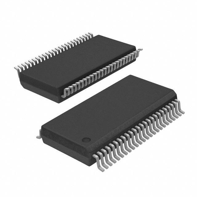
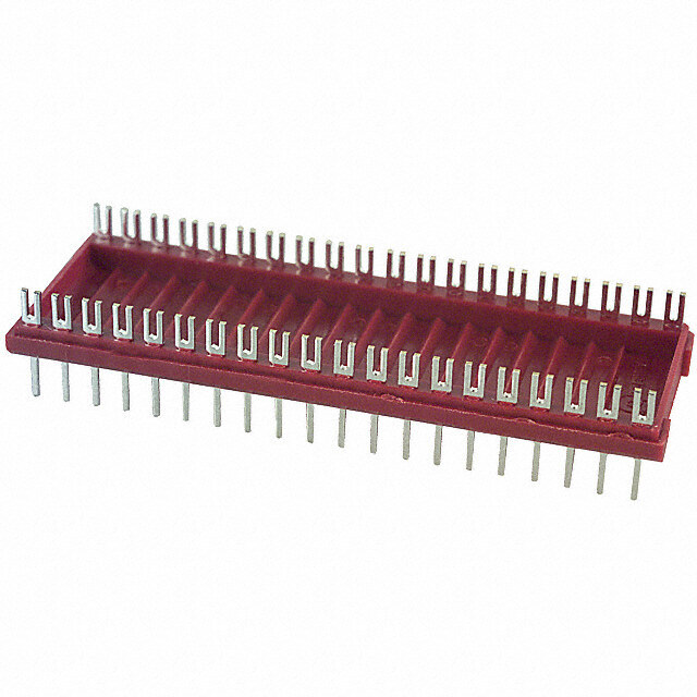
| 描述 | IC BUFF/DVR TRI-ST 16BIT 48SSOP |
| 产品分类 | |
| 品牌 | Texas Instruments |
| 数据手册 | |
| 产品图片 |
|
| 产品型号 | SN74LVTH16241DL |
| rohs | 无铅 / 符合限制有害物质指令(RoHS)规范要求 |
| 产品系列 | 74LVTH |
| 产品目录页面 | |
| 供应商器件封装 | 48-SSOP |
| 元件数 | 4 |
| 其它名称 | 296-12919-5 |
| 包装 | 管件 |
| 安装类型 | 表面贴装 |
| 封装/外壳 | 48-BSSOP(0.295",7.50mm 宽) |
| 工作温度 | -40°C ~ 85°C |
| 标准包装 | 25 |
| 每元件位数 | 4 |
| 电压-电源 | 2.7 V ~ 3.6 V |
| 电流-输出高,低 | 32mA,64mA |
| 逻辑类型 | 缓冲器/线路驱动器,非反相 |


.jpg)


PDF Datasheet 数据手册内容提取
SN54LVTH16241,, SN74LVTH16241 3.3-V ABT 16-BIT BUFFERS/DRIVERS WITH 3-STATE OUTPUTS www.ti.com SCBS693D–MAY1997–REVISEDNOVEMBER2006 FEATURES SN54LVTH16241 . . . WD PACKAGE • MembersoftheTexasInstrumentsWidebus™ SN74LVTH16241 . . . DGG OR DLPACKAGE Family (TOPVIEW) • State-of-the-ArtAdvancedBiCMOS 1OE 1 48 2OE Technology(ABT)Designfor3.3-VOperation 1Y1 2 47 1A1 andLowStatic-PowerDissipation 1Y2 3 46 1A2 • SupportMixed-ModeSignalOperation(5-V GND 4 45 GND InputandOutputVoltagesWith3.3-VV ) CC 1Y3 5 44 1A3 • SupportUnregulatedBatteryOperationDown 1Y4 6 43 1A4 to2.7V V 7 42 V CC CC • TypicalVOLP(OutputGroundBounce)<0.8V 2Y1 8 41 2A1 atVCC=3.3V,TA=25(cid:176) C 2Y2 9 40 2A2 • I andPower-Up3-StateSupportHot GND 10 39 GND off Insertion 2Y3 11 38 2A3 • BusHoldonDataInputsEliminatestheNeed 2Y4 12 37 2A4 forExternalPullup/PulldownResistors 3Y1 13 36 3A1 • DistributedV andGNDPinConfiguration 3Y2 14 35 3A2 CC GND 15 34 GND MinimizesHigh-SpeedSwitchingNoise 3Y3 16 33 3A3 • Flow-ThroughArchitectureOptimizesPCB 3Y4 17 32 3A4 Layout V 18 31 V • Latch-UpPerformanceExceeds500mAPer 4YCC1 19 30 4ACC1 JESD17 4Y2 20 29 4A2 • ESDProtectionExceeds2000VPer GND 21 28 GND MIL-STD-883,Method3015;Exceeds200V 4Y3 22 27 4A3 UsingMachineModel(C=200pF,R=0) 4Y4 23 26 4A4 • PackageOptionsIncludePlasticShrink 4OE 24 25 3OE Small-Outline(DL)andThinShrink Small-Outline(DGG)Packagesand380-mil Fine-PitchCeramicFlat(WD)PackageUsing 25-milCenter-to-CenterSpacings DESCRIPTION/ORDERING INFORMATION These 16-bit buffers/drivers are designed specifically for low-voltage (3.3-V) V operation, but with the CC capabilitytoprovideaTTLinterfacetoa5-Vsystemenvironment. The devices can be used as four 4-bit buffers, two 8-bit buffers, or one 16-bit buffer. The devices provide noninvertingoutputsandcomplementaryoutput-enable(OEandOE)inputs. ORDERINGINFORMATION T PACKAGE(1) ORDERABLEPARTNUMBER TOP-SIDEMARKING A 74LVTH16241DLRG4 Reelof1000 SN74LVTH16241DLR SSOP–DL LVTH16241 SN74LVTH16241DL –40(cid:176) Cto85(cid:176) C Tubeof25 SN74LVTH16241DLG4 74LVTH16241DGGRE4 TSSOP–DGG Reelof2000 LVTH16241 SN74LVTH16241DGGR (1) Packagedrawings,standardpackingquantities,thermaldata,symbolization,andPCBdesignguidelinesareavailableat www.ti.com/sc/package. Pleasebeawarethatanimportantnoticeconcerningavailability,standardwarranty,anduseincriticalapplicationsofTexas Instrumentssemiconductorproductsanddisclaimerstheretoappearsattheendofthisdatasheet. WidebusisatrademarkofTexasInstruments. PRODUCTIONDATAinformationiscurrentasofpublicationdate. Copyright©1997–2006,TexasInstrumentsIncorporated Products conform to specifications per the terms of the Texas Instruments standard warranty. Production processing does not necessarilyincludetestingofallparameters.
SN54LVTH16241,, SN74LVTH16241 3.3-V ABT 16-BIT BUFFERS/DRIVERS WITH 3-STATE OUTPUTS www.ti.com SCBS693D–MAY1997–REVISEDNOVEMBER2006 DESCRIPTION/ORDERING INFORMATION (CONTINUED) When V is between 0 and 1.5 V, the devices are in the high-impedance state during power up or power down. CC However, to ensure the high-impedance state above 1.5 V, OE should be tied to V through a pullup resistor CC and OE should be tied to GND through a pulldown resistor; the minimum value of the resistor is determined by thecurrent-sinking/current-sourcingcapabilityofthedriver. Activebus-holdcircuitryisprovidedtoholdunusedorfloatingdatainputsatavalidlogiclevel. These devices are fully specified for hot-insertion applications using I and power-up 3-state. The I circuitry off off disables the outputs, preventing damaging current backflow through the devices when they are powered down. The power-up 3-state circuitry places the outputs in the high-impedance state during power up and power down, whichpreventsdriverconflict. The SN54LVTH16241 is characterized for operation over the full military temperature range of –55(cid:176) C to 125(cid:176) C. TheSN74LVTH16241ischaracterizedforoperationfrom–40(cid:176) Cto85(cid:176) C. FUNCTIONTABLES INPUTS OUTPUTS 1OE,4OE 1A,4A 1Y,4Y L H H L L L H X Z INPUTS OUTPUTS 2OE,3OE 2A,3A 2Y,3Y H H H H L L L X Z 2 SubmitDocumentationFeedback
SN54LVTH16241,, SN74LVTH16241 3.3-V ABT 16-BIT BUFFERS/DRIVERS WITH 3-STATE OUTPUTS www.ti.com SCBS693D–MAY1997–REVISEDNOVEMBER2006 LOGICSYMBOL(A) 1 1OE EN1 48 2OE EN2 25 3OE EN3 24 4OE EN4 47 2 1A1 1 1 1Y1 46 3 1A2 1Y2 44 5 1A3 1Y3 43 6 1A4 1Y4 41 8 2A1 1 2 2Y1 40 9 2A2 2Y2 38 11 2A3 2Y3 37 12 2A4 2Y4 36 13 3A1 1 3 3Y1 35 14 3A2 3Y2 33 16 3A3 3Y3 32 17 3A4 3Y4 30 19 4A1 1 4 4Y1 29 20 4A2 4Y2 27 22 4A3 4Y3 26 23 4A4 4Y4 A. ThissymbolisinaccordancewithANSI/IEEEStd91-1984andIECPublication617-12. SubmitDocumentationFeedback 3
SN54LVTH16241,, SN74LVTH16241 3.3-V ABT 16-BIT BUFFERS/DRIVERS WITH 3-STATE OUTPUTS www.ti.com SCBS693D–MAY1997–REVISEDNOVEMBER2006 LOGICDIAGRAM(POSITIVELOGIC) 1 25 1OE 3OE 47 2 36 13 1A1 1Y1 3A1 3Y1 46 3 35 14 1A2 1Y2 3A2 3Y2 44 5 33 16 1A3 1Y3 3A3 3Y3 43 6 32 17 1A4 1Y4 3A4 3Y4 48 24 2OE 4OE 41 8 30 19 2A1 2Y1 4A1 4Y1 40 9 29 20 2A2 2Y2 4A2 4Y2 38 11 27 22 2A3 2Y3 4A3 4Y3 37 12 26 23 2A4 2Y4 4A4 4Y4 4 SubmitDocumentationFeedback
SN54LVTH16241,, SN74LVTH16241 3.3-V ABT 16-BIT BUFFERS/DRIVERS WITH 3-STATE OUTPUTS www.ti.com SCBS693D–MAY1997–REVISEDNOVEMBER2006 Absolute Maximum Ratings(1) overoperatingfree-airtemperaturerange(unlessotherwisenoted) MIN MAX UNIT V Supplyvoltagerange –0.5 4.6 V CC V Inputvoltagerange(2) –0.5 7 V I V Voltagerangeappliedtoanyoutputinthehigh-impedanceorpower-offstate(2) –0.5 7 V O V Voltagerangeappliedtoanyoutputinthehighstate(2) –0.5 V +0.5 V O CC SN54LVTH16241 96 I Currentintoanyoutputinthelowstate mA O SN74LVTH16241 128 SN54LVTH16241 48 I Currentintoanyoutputinthehighstate(3) mA O SN74LVTH16241 64 I Inputclampcurrent V <0 –50 mA IK I I Outputclampcurrent V <0 –50 mA OK O DGGpackage 89 q Packagethermalimpedance(4) (cid:176) C/W JA DLpackage 94 T Storagetemperaturerange –65 150 (cid:176) C stg (1) Stressesbeyondthoselistedunder"absolutemaximumratings"maycausepermanentdamagetothedevice.Thesearestressratings only,andfunctionaloperationofthedeviceattheseoranyotherconditionsbeyondthoseindicatedunder"recommendedoperating conditions"isnotimplied.Exposuretoabsolute-maximum-ratedconditionsforextendedperiodsmayaffectdevicereliability. (2) Theinputandoutputnegative-voltageratingsmaybeexceedediftheinputandoutputclamp-currentratingsareobserved. (3) ThiscurrentflowsonlywhentheoutputisinthehighstateandV >V . O CC (4) ThepackagethermalimpedanceiscalculatedinaccordancewithJESD51. Recommended Operating Conditions(1) SN54LVTH16241(2) SN74LVTH16241 UNIT MIN MAX MIN MAX V Supplyvoltage 2.7 3.6 2.7 3.6 V CC V High-levelinputvoltage 2 2 V IH V Low-levelinputvoltage 0.8 0.8 V IL V Inputvoltage 5.5 5.5 V I I High-leveloutputcurrent –24 –32 mA OH I Low-leveloutputcurrent 48 64 mA OL D t/D v Inputtransitionriseorfallrate Outputsenabled 10 10 ns/V D t/D V Power-upramprate 200 200 m s/V CC T Operatingfree-airtemperature –55 125 –40 85 (cid:176) C A (1) AllunusedcontrolinputsofthedevicemustbeheldatV orGNDtoensureproperdeviceoperation.RefertotheTIapplicationreport, CC ImplicationsofSloworFloatingCMOSInputs,literaturenumberSCBA004. (2) ProductPreview SubmitDocumentationFeedback 5
SN54LVTH16241,, SN74LVTH16241 3.3-V ABT 16-BIT BUFFERS/DRIVERS WITH 3-STATE OUTPUTS www.ti.com SCBS693D–MAY1997–REVISEDNOVEMBER2006 Electrical Characteristics overrecemmendedoperatingfree-airtemperaturerange(unlessotherwisenoted) SN54LVTH16241(1) SN74LVTH16241 PARAMETER TESTCONDITIONS UNIT MIN TYP(2) MAX MIN TYP(2) MAX V V =2.7V, I =–18mA –1.2 –1.2 V IK CC I V =2.7Vto3.6V, I =–100m A V –0.2 V –0.2 CC OH CC CC V =2.7V, I =–8mA 2.4 2.4 CC OH V V OH I =–24mA 2 OH V =3V CC I =–32mA 2 OH I =100m A 0.2 0.2 OL V =2.7V CC I =24mA 0.5 0.5 OL I =16mA 0.4 0.4 OL V V OL I =32mA 0.5 0.5 OL V =3V CC I =48mA 0.55 OL I =64mA 0.55 OL V =0or3.6V, V =5.5V 10 10 CC I Control V =3.6V, V =V orGND – 1 – 1 I inputs CC I CC m A I V =V 1 1 I CC Datainputs V =3.6V CC V =0 –5 –5 I I V =0, V orV =0to4.5V – 100 – 100 m A off CC I O V =0.8V 75 75 I V =3V CC I Datainputs VI=2V –75 –75 m A I(hold) 500 V =3.6V(3), V =0to3.6V CC I –750 I V =3.6V, V =3V 5 5 m A OZH CC O I V =3.6V, V =0.5V –5 –5 m A OZL CC O I VCC=0to1.5V,VO=0.5Vto3V, – 100(4) – 100 m A OZPU OE/OE=don'tcare I VCC=1.5Vto0,VO=0.5Vto3V, – 100(4) – 100 m A OZPD OE/OE=don'tcare Outputshigh 0.19 0.19 V =3.6V, CC I I =0, Outputslow 5 5 mA CC O V =V orGND I CC Outputsdisabled 0.19 0.19 D I (5) VCC=3Vto3.6V,OneinputatVCC–0.6V, 0.2 0.2 mA CC OtherinputsatV orGND CC C V =3Vor0 4 4 pF i I C V =3Vor0 9 9 pF o O (1) ProductPreview (2) AlltypicalvaluesareatV =3.3V,T =25(cid:176) C. CC A (3) Thisisthebus-holdmaximumdynamiccurrent.Itistheminimumoverdrivecurrentrequiredtoswitchtheinputfromonestateto another. (4) OnproductscomplianttoMIL-PRF-38535,thisparameterisnotproductiontested. (5) ThisistheincreaseinsupplycurrentforeachinputthatisatthespecifiedTTLvoltagelevel,ratherthanV orGND. CC 6 SubmitDocumentationFeedback
SN54LVTH16241,, SN74LVTH16241 3.3-V ABT 16-BIT BUFFERS/DRIVERS WITH 3-STATE OUTPUTS www.ti.com SCBS693D–MAY1997–REVISEDNOVEMBER2006 Switching Characteristics overrecommendedoperatingfree-airtemperaturerange,C =50pF(unlessotherwisenoted)(seeFigure1) L FROM TO SN54LVTH16241(1) SN74LVTH16241 PARAMETER UNIT (INPUT) (OUTPUT) MIN MAX MIN MAX MIN TYP(2) MAX MIN MAX t 1.1 3.7 4 1.2 2.6 3.5 3.8 PLH A Y ns t 1.1 3.7 4 1.2 2.2 3.5 3.8 PHL t 1.1 4.7 5.3 1.2 3.2 4.5 5.1 PZH OEorOE Y ns t 1.1 4.7 5.2 1.2 3.2 4.5 4.9 PZL t 1.9 5.5 6.1 2 3.7 5.3 5.9 PHZ OEorOE Y ns t 1.9 5.2 5.7 2 3.4 4.9 5.4 PLZ t 0.5 0.5 sk(LH) ns t 0.5 0.5 sk(HL) (1) ProductPreview (2) AlltypicalvaluesareatV =3.3V,T =25(cid:176) C. CC A SubmitDocumentationFeedback 7
SN54LVTH16241,, SN74LVTH16241 3.3-V ABT 16-BIT BUFFERS/DRIVERS WITH 3-STATE OUTPUTS www.ti.com SCBS693D–MAY1997–REVISEDNOVEMBER2006 PARAMETER MEASUREMENT INFORMATION 6 V From Output 500W S1 Open TEST S1 Under Test GND t /t Open PLH PHL (seCeL N= o5t0e pAF) 500W ttPPHLZZ//ttPPZZLH G6N VD 2.7 V LOAD CIRCUIT Timing Input 1.5 V 0 V t w t t su h 2.7 V 2.7 V Input 1.5 V 1.5 V Data Input 1.5 V 1.5 V 0 V 0 V VOLTAGE WAVEFORMS VOLTAGE WAVEFORMS PULSE DURATION SETUPAND HOLD TIMES 2.7 V 2.7 V Input 1.5 V 1.5 V Output 1.5 V 1.5 V Control 0 V 0 V tPLH tPHL Output tPZL tPLZ VOH Waveform 1 3 V Output 1.5 V 1.5 V S1 at 6 V 1.5 V V + 0.3 V V (see Note B) OL V OL OL t t t t PHL PLH PZH PHZ Output V V Output 1.5 V 1.5 V OH WSa1v eafto GrmN D2 1.5 V VOH–0.3 V OH V (see Note B) »0 V OL VOLTAGE WAVEFORMS VOLTAGE WAVEFORMS PROPAGATION DELAYTIMES ENABLEAND DISABLE TIMES INVERTINGAND NONINVERTING OUTPUTS LOW-AND HIGH-LEVELENABLING NOTES: A. C includes probe and jig capacitance. L B. Waveform 1 is for an output with internal conditions such that the output is low, except when disabled by the output control. Waveform 2 is for an output with internal conditions such that the output is high, except when disabled by the output control. C. All input pulses are supplied by generators having the following characteristics: PRR£10 MHz, Z = 50W, t £2.5 ns, t £2.5 ns. O r f D. The outputs are measured one at a time, with one transition per measurement. Figure1.LoadCircuitandVoltageWaveforms 8 SubmitDocumentationFeedback
PACKAGE OPTION ADDENDUM www.ti.com 6-Feb-2020 PACKAGING INFORMATION Orderable Device Status Package Type Package Pins Package Eco Plan Lead/Ball Finish MSL Peak Temp Op Temp (°C) Device Marking Samples (1) Drawing Qty (2) (6) (3) (4/5) SN74LVTH16241DGGR ACTIVE TSSOP DGG 48 2000 Green (RoHS NIPDAU Level-1-260C-UNLIM -40 to 85 LVTH16241 & no Sb/Br) SN74LVTH16241DL ACTIVE SSOP DL 48 25 Green (RoHS NIPDAU Level-1-260C-UNLIM -40 to 85 LVTH16241 & no Sb/Br) (1) The marketing status values are defined as follows: ACTIVE: Product device recommended for new designs. LIFEBUY: TI has announced that the device will be discontinued, and a lifetime-buy period is in effect. NRND: Not recommended for new designs. Device is in production to support existing customers, but TI does not recommend using this part in a new design. PREVIEW: Device has been announced but is not in production. Samples may or may not be available. OBSOLETE: TI has discontinued the production of the device. (2) RoHS: TI defines "RoHS" to mean semiconductor products that are compliant with the current EU RoHS requirements for all 10 RoHS substances, including the requirement that RoHS substance do not exceed 0.1% by weight in homogeneous materials. Where designed to be soldered at high temperatures, "RoHS" products are suitable for use in specified lead-free processes. TI may reference these types of products as "Pb-Free". RoHS Exempt: TI defines "RoHS Exempt" to mean products that contain lead but are compliant with EU RoHS pursuant to a specific EU RoHS exemption. Green: TI defines "Green" to mean the content of Chlorine (Cl) and Bromine (Br) based flame retardants meet JS709B low halogen requirements of <=1000ppm threshold. Antimony trioxide based flame retardants must also meet the <=1000ppm threshold requirement. (3) MSL, Peak Temp. - The Moisture Sensitivity Level rating according to the JEDEC industry standard classifications, and peak solder temperature. (4) There may be additional marking, which relates to the logo, the lot trace code information, or the environmental category on the device. (5) Multiple Device Markings will be inside parentheses. Only one Device Marking contained in parentheses and separated by a "~" will appear on a device. If a line is indented then it is a continuation of the previous line and the two combined represent the entire Device Marking for that device. (6) Lead/Ball Finish - Orderable Devices may have multiple material finish options. Finish options are separated by a vertical ruled line. Lead/Ball Finish values may wrap to two lines if the finish value exceeds the maximum column width. Important Information and Disclaimer:The information provided on this page represents TI's knowledge and belief as of the date that it is provided. TI bases its knowledge and belief on information provided by third parties, and makes no representation or warranty as to the accuracy of such information. Efforts are underway to better integrate information from third parties. TI has taken and continues to take reasonable steps to provide representative and accurate information but may not have conducted destructive testing or chemical analysis on incoming materials and chemicals. TI and TI suppliers consider certain information to be proprietary, and thus CAS numbers and other limited information may not be available for release. In no event shall TI's liability arising out of such information exceed the total purchase price of the TI part(s) at issue in this document sold by TI to Customer on an annual basis. Addendum-Page 1
PACKAGE OPTION ADDENDUM www.ti.com 6-Feb-2020 Addendum-Page 2
PACKAGE MATERIALS INFORMATION www.ti.com 11-Mar-2017 TAPE AND REEL INFORMATION *Alldimensionsarenominal Device Package Package Pins SPQ Reel Reel A0 B0 K0 P1 W Pin1 Type Drawing Diameter Width (mm) (mm) (mm) (mm) (mm) Quadrant (mm) W1(mm) SN74LVTH16241DGGR TSSOP DGG 48 2000 330.0 24.4 8.6 13.0 1.8 12.0 24.0 Q1 PackMaterials-Page1
PACKAGE MATERIALS INFORMATION www.ti.com 11-Mar-2017 *Alldimensionsarenominal Device PackageType PackageDrawing Pins SPQ Length(mm) Width(mm) Height(mm) SN74LVTH16241DGGR TSSOP DGG 48 2000 367.0 367.0 45.0 PackMaterials-Page2
MECHANICAL DATA MTSS003D – JANUARY 1995 – REVISED JANUARY 1998 DGG (R-PDSO-G**) PLASTIC SMALL-OUTLINE PACKAGE 48 PINS SHOWN 0,27 0,50 0,08 M 0,17 48 25 6,20 8,30 6,00 7,90 0,15 NOM Gage Plane 0,25 1 24 0°–8° A 0,75 0,50 Seating Plane 0,15 1,20 MAX 0,10 0,05 PINS ** 48 56 64 DIM A MAX 12,60 14,10 17,10 A MIN 12,40 13,90 16,90 4040078/F 12/97 NOTES: A. All linear dimensions are in millimeters. B. This drawing is subject to change without notice. C. Body dimensions do not include mold protrusion not to exceed 0,15. D. Falls within JEDEC MO-153 • POST OFFICE BOX 655303 DALLAS, TEXAS 75265
None
IMPORTANTNOTICEANDDISCLAIMER TI PROVIDES TECHNICAL AND RELIABILITY DATA (INCLUDING DATASHEETS), DESIGN RESOURCES (INCLUDING REFERENCE DESIGNS), APPLICATION OR OTHER DESIGN ADVICE, WEB TOOLS, SAFETY INFORMATION, AND OTHER RESOURCES “AS IS” AND WITH ALL FAULTS, AND DISCLAIMS ALL WARRANTIES, EXPRESS AND IMPLIED, INCLUDING WITHOUT LIMITATION ANY IMPLIED WARRANTIES OF MERCHANTABILITY, FITNESS FOR A PARTICULAR PURPOSE OR NON-INFRINGEMENT OF THIRD PARTY INTELLECTUAL PROPERTY RIGHTS. These resources are intended for skilled developers designing with TI products. You are solely responsible for (1) selecting the appropriate TI products for your application, (2) designing, validating and testing your application, and (3) ensuring your application meets applicable standards, and any other safety, security, or other requirements. These resources are subject to change without notice. TI grants you permission to use these resources only for development of an application that uses the TI products described in the resource. Other reproduction and display of these resources is prohibited. No license is granted to any other TI intellectual property right or to any third party intellectual property right. TI disclaims responsibility for, and you will fully indemnify TI and its representatives against, any claims, damages, costs, losses, and liabilities arising out of your use of these resources. TI’s products are provided subject to TI’s Terms of Sale (www.ti.com/legal/termsofsale.html) or other applicable terms available either on ti.com or provided in conjunction with such TI products. TI’s provision of these resources does not expand or otherwise alter TI’s applicable warranties or warranty disclaimers for TI products. Mailing Address: Texas Instruments, Post Office Box 655303, Dallas, Texas 75265 Copyright © 2020, Texas Instruments Incorporated