ICGOO在线商城 > 集成电路(IC) > 逻辑 - 缓冲器,驱动器,接收器,收发器 > SN74LVCH32245AZKER
 Datasheet下载
- 型号: SN74LVCH32245AZKER
- 制造商: Texas Instruments
- 库位|库存: xxxx|xxxx
- 要求:
| 数量阶梯 | 香港交货 | 国内含税 |
| +xxxx | $xxxx | ¥xxxx |
查看当月历史价格
查看今年历史价格
SN74LVCH32245AZKER产品简介:
ICGOO电子元器件商城为您提供SN74LVCH32245AZKER由Texas Instruments设计生产,在icgoo商城现货销售,并且可以通过原厂、代理商等渠道进行代购。 SN74LVCH32245AZKER价格参考。Texas InstrumentsSN74LVCH32245AZKER封装/规格:逻辑 - 缓冲器,驱动器,接收器,收发器, Transceiver, Non-Inverting 4 Element 8 Bit per Element 3-State Output 96-PBGA MICROSTAR (13.6x5.6)。您可以下载SN74LVCH32245AZKER参考资料、Datasheet数据手册功能说明书,资料中有SN74LVCH32245AZKER 详细功能的应用电路图电压和使用方法及教程。
SN74LVCH32245AZKER是德州仪器(Texas Instruments)生产的一款逻辑器件,属于缓冲器、驱动器、接收器和收发器类别。该型号的主要应用场景包括数据总线切换、信号电平转换以及多路信号传输等。

 应用场景

1. 数据总线切换:
   - SN74LVCH32245AZKER可以用于在不同的数据总线之间进行切换。它具有两个独立的双向总线接口,可以在两个方向上传输数据。这种特性使其非常适合用于需要频繁切换数据路径的应用,例如在计算机系统中,当需要将不同设备的数据传输到同一总线上时。

2. 信号电平转换:
   - 该器件支持不同的电压电平转换,适用于低电压逻辑电平(如1.65V至5.5V)之间的信号传输。这使得它能够在不同电压域的电路之间进行通信,例如在现代嵌入式系统中,CPU和其他外设可能工作在不同的电压电平,SN74LVCH32245AZKER可以确保这些设备之间的信号兼容性和完整性。

3. 多路信号传输:
   - 由于其双向传输能力,SN74LVCH32245AZKER可以同时处理多个信号路径。这在需要高效管理多个输入输出信号的应用中非常有用,例如在工业控制系统、通信设备或消费电子产品的多通道数据传输中。

4. 噪声抑制与信号完整性:
   - 该器件内置了噪声抑制功能,能够减少信号传输过程中的干扰,确保信号的完整性和可靠性。这对于高速信号传输尤为重要,特别是在长距离传输或多节点网络中。

5. 电源管理与节能:
   - SN74LVCH32245AZKER还具备低功耗特性,适合用于对功耗敏感的应用,如便携式设备、电池供电系统等。其待机模式可以进一步降低功耗,延长设备的续航时间。

 总结
SN74LVCH32245AZKER是一款多功能的逻辑器件,广泛应用于数据总线切换、信号电平转换、多路信号传输等领域。它不仅提供了可靠的信号传输性能,还具备低功耗和噪声抑制等优点,适用于各种复杂和高性能的电子系统。
| 参数 | 数值 |
| 产品目录 | 集成电路 (IC)半导体 |
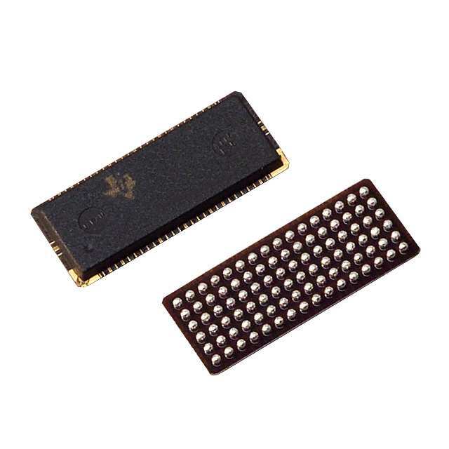
| 描述 | IC BUS TRANSCVR 32BIT 96BGA总线收发器 32-Bit Bus Trnscvr W/3-State Output |
| 产品分类 | |
| 品牌 | Texas Instruments |
| 产品手册 | |
| 产品图片 |
|
| rohs | 符合RoHS无铅 / 符合限制有害物质指令(RoHS)规范要求 |
| 产品系列 | 逻辑集成电路,总线收发器,Texas Instruments SN74LVCH32245AZKER74LVCH |
| 数据手册 | |
| 产品型号 | SN74LVCH32245AZKER |
| PCN设计/规格 | |
| 产品目录页面 | |
| 产品种类 | 总线收发器 |
| 传播延迟时间 | 4 ns |
| 低电平输出电流 | 24 mA |
| 供应商器件封装 | 96-PBGA MICROSTAR(13.6x5.6) |
| 元件数 | 8 |
| 其它名称 | 296-23285-6 |
| 功能 | Bus Transceiver |
| 包装 | Digi-Reel® |
| 单位重量 | 166.600 mg |
| 商标 | Texas Instruments |
| 安装类型 | 表面贴装 |
| 安装风格 | SMD/SMT |
| 封装 | Reel |
| 封装/外壳 | 96-LFBGA |
| 封装/箱体 | BGA-96 Microstar |
| 工作温度 | -40°C ~ 85°C |
| 工厂包装数量 | 1000 |
| 最大工作温度 | + 85 C |
| 最小工作温度 | - 40 C |
| 极性 | Non-Inverting |
| 标准包装 | 1 |
| 每元件位数 | 4 |
| 每芯片的通道数量 | 32 |
| 电压-电源 | 1.65 V ~ 3.6 V |
| 电流-输出高,低 | 24mA,24mA |
| 电源电压-最大 | 3.6 V |
| 电源电压-最小 | 1.65 V |
| 电路数量 | 4 |
| 系列 | SN74LVCH32245A |
| 输入电平 | TTL/CMOS |
| 输出电平 | LVTTL |
| 输出类型 | 3-State |
| 逻辑类型 | 收发器,非反相 |
| 逻辑系列 | LVC |
| 高电平输出电流 | - 24 mA |


.jpg)


PDF Datasheet 数据手册内容提取
SN74LVCH32245A 32-BIT BUS TRANSCEIVER WITH 3-STATE OUTPUTS www.ti.com SCAS616H–OCTOBER1998–REVISEDMARCH2005 FEATURES • SupportsMixed-ModeSignalOperationon • MemberoftheTexasInstrumentsWidebus+™ AllPorts(5-VInput/OutputVoltageWith Family 3.3-VVCC) • OperatesFrom1.65Vto3.6V • BusHoldonDataInputsEliminatestheNeed • InputsAcceptVoltagesto5.5V forExternalPullup/PulldownResistors • Maxt of4nsat3.3V • OtherProductstoConsider:SN74LVC32245 • TypicpadlV (OutputGroundBounce) • Latch-UpPerformanceExceeds100mAPer <0.8VatOVLP =3.3V,T =25(cid:176) C JESD78,ClassII • TypicalV CC(OutputVA Undershoot) • ESDProtectionExceedsJESD22 OHV OH >2VatV =3.3V,T =25(cid:176) C – 2000-VHuman-BodyModel(A114-A) CC A • I SupportsPartial-Power-DownMode – 200-VMachineModel(A115-A) off Operation – 1000-VCharged-DeviceModel(C101) DESCRIPTION/ORDERING INFORMATION This32-bit(quad-octal)noninvertingbustransceiverisdesignedfor1.65-Vto3.6-VV operation. CC The SN74LVCH32245A is designed for asynchronous communication between data buses. The control-function implementationminimizesexternaltimingrequirements. This device can be used as four 8-bit transceivers, two 16-bit transceivers, or one 32-bit transceiver. It allows data transmission from the A bus to the B bus or from the B bus to the A bus, depending on the logic level at the direction-control (DIR) input. The output-enable (OE) input can be used to disable the device so that the buses effectivelyareisolated. Inputs can be driven from either 3.3-V or 5-V devices. This feature allows the use of these devices as translators inamixed3.3-V/5-Vsystemenvironment. This device is fully specified for partial-power-down applications using I . The I circuitry disables the outputs, off off preventingdamagingcurrentbackflowthroughthedevicewhenitispowereddown. To ensure the high-impedance state during power up or power down, OE should be tied to V through a pullup CC resistor;theminimumvalueoftheresistorisdeterminedbythecurrent-sinkingcapabilityofthedriver. Active bus-hold circuitry is provided to hold unused or floating data inputs at a valid logic level. Use of pullup or pulldown resistors with the bus-hold circuitry is not recommended. The bus-hold circuitry is part of the input circuitandisnotdisabledbyOEorDIR. ORDERINGINFORMATION T PACKAGE(1) ORDERABLEPARTNUMBER TOP-SIDEMARKING A LFBGA–GKE SN74LVCH32245AGKER –40(cid:176) Cto85(cid:176) C Tapeandreel CH245A LFBGA–ZKE(Pb-free) SN74LVCH32245AZKER (1) Packagedrawings,standardpackingquantities,thermaldata,symbolization,andPCBdesignguidelinesareavailableat www.ti.com/sc/package. Pleasebeawarethatanimportantnoticeconcerningavailability,standardwarranty,anduseincriticalapplicationsofTexas Instrumentssemiconductorproductsanddisclaimerstheretoappearsattheendofthisdatasheet. Widebus+isatrademarkofTexasInstruments. PRODUCTIONDATAinformationiscurrentasofpublicationdate. Copyright©1998–2005,TexasInstrumentsIncorporated Products conform to specifications per the terms of the Texas Instruments standard warranty. Production processing does not necessarilyincludetestingofallparameters.
SN74LVCH32245A 32-BIT BUS TRANSCEIVER WITH 3-STATE OUTPUTS www.ti.com SCAS616H–OCTOBER1998–REVISEDMARCH2005 GKE OR ZKE PACKAGE TERMINALASSIGNMENTS (TOP VIEW) 1 2 3 4 5 6 1 2 3 4 5 6 A 1B2 1B1 1DIR 1OE 1A1 1A2 B 1B4 1B3 GND GND 1A3 1A4 A C 1B6 1B5 V V 1A5 1A6 CC CC B D 1B8 1B7 GND GND 1A7 1A8 C E 2B2 2B1 GND GND 2A1 2A2 D F 2B4 2B3 V V 2A3 2A4 CC CC E G 2B6 2B5 GND GND 2A5 2A6 F H 2B7 2B8 2DIR 2OE 2A8 2A7 G J 3B2 3B1 3DIR 3OE 3A1 3A2 K 3B4 3B3 GND GND 3A3 3A4 H L 3B6 3B5 V V 3A5 3A6 J CC CC M 3B8 3B7 GND GND 3A7 3A8 K N 4B2 4B1 GND GND 4A1 4A2 L P 4B4 4B3 V V 4A3 4A4 CC CC M R 4B6 4B5 GND GND 4A5 4A6 N T 4B7 4B8 4DIR 4OE 4A8 4A7 P R T FUNCTIONTABLE (EACH8-BITSECTION) INPUTS OPERATION OE DIR L L BdatatoAbus L H AdatatoBbus H X Isolation 2
SN74LVCH32245A 32-BIT BUS TRANSCEIVER WITH 3-STATE OUTPUTS www.ti.com SCAS616H–OCTOBER1998–REVISEDMARCH2005 LOGICDIAGRAM(POSITIVELOGIC) A3 H3 1DIR 2DIR A4 H4 1OE 2OE A5 E5 1A1 2A1 A2 E2 1B1 2B1 To Seven Other Channels To Seven Other Channels J3 T3 3DIR 4DIR J4 T4 3OE 4OE J5 N5 3A1 4A1 J2 N2 3B1 4B1 To Seven Other Channels To Seven Other Channels 3
SN74LVCH32245A 32-BIT BUS TRANSCEIVER WITH 3-STATE OUTPUTS www.ti.com SCAS616H–OCTOBER1998–REVISEDMARCH2005 Absolute Maximum Ratings(1) overoperatingfree-airtemperaturerange(unlessotherwisenoted) MIN MAX UNIT V Supplyvoltagerange –0.5 6.5 V CC V Inputvoltagerange(2) –0.5 6.5 V I V Voltagerangeappliedtoanyoutputinthehigh-impedanceorpower-offstate(2) –0.5 6.5 V O V Voltagerangeappliedtoanyoutputinthehighorlowstate(2)(3) –0.5 V +0.5 V O CC I Inputclampcurrent V <0 –50 mA IK I I Outputclampcurrent V <0 –50 mA OK O I Continuousoutputcurrent – 50 mA O ContinuouscurrentthrougheachV orGND – 100 mA CC q Packagethermalimpedance(4) GKE/ZKEpackage 40 (cid:176) C/W JA T Storagetemperaturerange –65 150 (cid:176) C stg (1) Stressesbeyondthoselistedunder"absolutemaximumratings"maycausepermanentdamagetothedevice.Thesearestressratings only,andfunctionaloperationofthedeviceattheseoranyotherconditionsbeyondthoseindicatedunder"recommendedoperating conditions"isnotimplied.Exposuretoabsolute-maximum-ratedconditionsforextendedperiodsmayaffectdevicereliability. (2) Theinputnegative-voltageandoutputvoltageratingsmaybeexceedediftheinputandoutputcurrentratingsareobserved. (3) ThevalueofV isprovidedintherecommendedoperatingconditionstable. CC (4) ThepackagethermalimpedanceiscalculatedinaccordancewithJESD51-7. Recommended Operating Conditions(1) MIN MAX UNIT Operating 1.65 3.6 V Supplyvoltage V CC Dataretentiononly 1.5 V =1.65Vto1.95V 0.65· V CC CC V High-levelinputvoltage V =2.3Vto2.7V 1.7 V IH CC V =2.7Vto3.6V 2 CC V =1.65Vto1.95V 0.35· V CC CC V Low-levelinputvoltage V =2.3Vto2.7V 0.7 V IL CC V =2.7Vto3.6V 0.8 CC V Inputvoltage 0 5.5 V I Highorlowstate 0 V CC V Outputvoltage V O 3-state 0 5.5 V =1.65V –4 CC V =2.3V –8 CC I High-leveloutputcurrent mA OH V =2.7V –12 CC V =3V –24 CC V =1.65V 4 CC V =2.3V 8 CC I Low-leveloutputcurrent mA OL V =2.7V 12 CC V =3V 24 CC D t/D v Inputtransitionriseorfallrate 5 ns/V T Operatingfree-airtemperature –40 85 (cid:176) C A (1) AllunusedcontrolinputsofthedevicemustbeheldatV orGNDtoensureproperdeviceoperation.RefertotheTIapplicationreport, CC ImplicationsofSloworFloatingCMOSInputs,literaturenumberSCBA004. 4
SN74LVCH32245A 32-BIT BUS TRANSCEIVER WITH 3-STATE OUTPUTS www.ti.com SCAS616H–OCTOBER1998–REVISEDMARCH2005 Electrical Characteristics overrecommendedoperatingfree-airtemperaturerange(unlessotherwisenoted) PARAMETER TESTCONDITIONS V MIN TYP(1) MAX UNIT CC I =–100m A 1.65Vto3.6V V –0.2 OH CC I =–4mA 1.65V 1.2 OH I =–8mA 2.3V 1.7 OH V V OH 2.7V 2.2 I =–12mA OH 3V 2.4 I =–24mA 3V 2.2 OH I =100m A 1.65Vto3.6V 0.2 OL I =4mA 1.65V 0.45 OL V I =8mA 2.3V 0.7 V OL OL I =12mA 2.7V 0.4 OL I =24mA 3V 0.55 OL I Controlinputs V =0to5.5V 3.6V – 5 m A I I V =0.58V 25 I 1.65V V =1.07V –25 I V =0.7V 45 I 2.3V I V =1.7V –45 m A I(hold) I V =0.8V 75 I 3V V =2V –75 I V =0to3.6V(2) 3.6V – 500 I I V orV =5.5V 0 – 10 m A off I O I (3) V =0Vor(V to5.5V) 3.6V – 10 m A OZ O CC V =V orGND 40 I I CC I =0 3.6V m A CC 3.6V£ V £ 5.5V(4) O 40 I D I OneinputatV –0.6V, OtherinputsatV orGND 2.7Vto3.6V 500 m A CC CC CC C Controlinputs V =V orGND 3.3V 5 pF i I CC C AorBports V =V orGND 3.3V 7.5 pF io O CC (1) AlltypicalvaluesareatV =3.3V,T =25(cid:176) C. CC A (2) Thisisthebus-holdmaximumdynamiccurrent.Itistheminimumoverdrivecurrentrequiredtoswitchtheinputfromonestateto another. (3) ForthetotalleakagecurrentinanI/Oport,pleaseconsulttheI specificationfortheinputvoltagecondition0V<V <V ,andthe I(hold) I CC I specificationfortheinputvoltageconditionsV =0VorV =V to5.5V.Thebus-holdcurrent,atinputvoltagegreaterthanV ,is OZ I I CC CC negligible. (4) Thisappliesinthedisabledstateonly. Switching Characteristics overrecommendedoperatingfree-airtemperaturerange(unlessotherwisenoted)(seeFigure1) V =1.8V V =2.5V V =3.3V PARAMETER FROM TO C– C0.15V C–C0.2V VCC=2.7V C–C0.3V UNIT (INPUT) (OUTPUT) MIN MAX MIN MAX MIN MAX MIN MAX t AorB BorA 1.5 7.1 1 4.5 1 4.7 1 4 ns pd t OE AorB 1.5 8.9 1 5.6 1.5 6.7 1.5 5.5 ns en t OE AorB 1.5 11.9 1 6.8 1.5 7.1 1.5 6.6 ns dis t 1.5 ns sk(o) 5
SN74LVCH32245A 32-BIT BUS TRANSCEIVER WITH 3-STATE OUTPUTS www.ti.com SCAS616H–OCTOBER1998–REVISEDMARCH2005 Operating Characteristics T =25(cid:176) C A TEST VCC=1.8V VCC=2.5V VCC=3.3V PARAMETER UNIT CONDITIONS TYP TYP TYP Outputsenabled 36 36 40 C Powerdissipationcapacitance f=10MHz pF pd Outputsdisabled 3 3 4 6
SN74LVCH32245A 32-BIT BUS TRANSCEIVER WITH 3-STATE OUTPUTS www.ti.com SCAS616H–OCTOBER1998–REVISEDMARCH2005 PARAMETER MEASUREMENT INFORMATION VLOAD From Output RL S1 Open TEST S1 Under Test GND tPLH/tPHL Open (see Note CAL) RL tPLZ/tPZL VLOAD tPHZ/tPZH GND LOAD CIRCUIT INPUTS VCC VI tr/tf VM VLOAD CL RL VD 1.8 V ± 0.15 V VCC ≤2 ns VCC/2 2 × VCC 30 pF 1 kW 0.15 V 2.5 V ± 0.2 V VCC ≤2 ns VCC/2 2 × VCC 30 pF 500 W 0.15 V 2.7 V 2.7 V ≤2.5 ns 1.5 V 6 V 50 pF 500 W 0.3 V 3.3 V ± 0.3 V 2.7 V ≤2.5 ns 1.5 V 6 V 50 pF 500 W 0.3 V VI Timing Input VM 0 V tw tsu th VI VI Input VM VM Data Input VM VM 0 V 0 V VOLTAGE WAVEFORMS VOLTAGE WAVEFORMS PULSE DURATION SETUP AND HOLD TIMES VI VI Output Input VM VM Control VM VM 0 V 0 V tPLH tPHL tPZL tPLZ Output VOH Waveform 1 VLOAD/2 Output VM VM VOL (Ss1e ea tN VoLteO ABD) VM VOL + VD VOL tPHL tPLH tPZH tPHZ Output VM VM VOH WSa1v eaOfto uGrtmpNu D2t VM VOH − VD VOH VOL (see Note B) ≈0 V VOLTAGE WAVEFORMS VOLTAGE WAVEFORMS PROPAGATION DELAY TIMES ENABLE AND DISABLE TIMES INVERTING AND NONINVERTING OUTPUTS LOW- AND HIGH-LEVEL ENABLING NOTES: A. CL includes probe and jig capacitance. B. Waveform 1 is for an output with internal conditions such that the output is low, except when disabled by the output control. Waveform2 is for an output with internal conditions such that the output is high, except when disabled by the output control. C. All input pulses are supplied by generators having the following characteristics: PRR ≤ 10 MHz, ZO = 50 W . D. The outputs are measured one at a time, with one transition per measurement. E. tPLZ and tPHZ are the same as tdis. F. tPZL and tPZH are the same as ten. G. tPLH and tPHL are the same as tpd. H. All parameters and waveforms are not applicable to all devices. Figure1.LoadCircuitandVoltageWaveforms 7
PACKAGE OPTION ADDENDUM www.ti.com 11-Apr-2013 PACKAGING INFORMATION Orderable Device Status Package Type Package Pins Package Eco Plan Lead/Ball Finish MSL Peak Temp Op Temp (°C) Top-Side Markings Samples (1) Drawing Qty (2) (3) (4) SN74LVCH32245AGKER NRND LFBGA GKE 96 1000 TBD SNPB Level-2-235C-1 YEAR -40 to 85 CH245A SN74LVCH32245AZKER ACTIVE LFBGA ZKE 96 1000 Green (RoHS SNAGCU Level-3-260C-168 HR -40 to 85 CH245A & no Sb/Br) (1) The marketing status values are defined as follows: ACTIVE: Product device recommended for new designs. LIFEBUY: TI has announced that the device will be discontinued, and a lifetime-buy period is in effect. NRND: Not recommended for new designs. Device is in production to support existing customers, but TI does not recommend using this part in a new design. PREVIEW: Device has been announced but is not in production. Samples may or may not be available. OBSOLETE: TI has discontinued the production of the device. (2) Eco Plan - The planned eco-friendly classification: Pb-Free (RoHS), Pb-Free (RoHS Exempt), or Green (RoHS & no Sb/Br) - please check http://www.ti.com/productcontent for the latest availability information and additional product content details. TBD: The Pb-Free/Green conversion plan has not been defined. Pb-Free (RoHS): TI's terms "Lead-Free" or "Pb-Free" mean semiconductor products that are compatible with the current RoHS requirements for all 6 substances, including the requirement that lead not exceed 0.1% by weight in homogeneous materials. Where designed to be soldered at high temperatures, TI Pb-Free products are suitable for use in specified lead-free processes. Pb-Free (RoHS Exempt): This component has a RoHS exemption for either 1) lead-based flip-chip solder bumps used between the die and package, or 2) lead-based die adhesive used between the die and leadframe. The component is otherwise considered Pb-Free (RoHS compatible) as defined above. Green (RoHS & no Sb/Br): TI defines "Green" to mean Pb-Free (RoHS compatible), and free of Bromine (Br) and Antimony (Sb) based flame retardants (Br or Sb do not exceed 0.1% by weight in homogeneous material) (3) MSL, Peak Temp. -- The Moisture Sensitivity Level rating according to the JEDEC industry standard classifications, and peak solder temperature. (4) Multiple Top-Side Markings will be inside parentheses. Only one Top-Side Marking contained in parentheses and separated by a "~" will appear on a device. If a line is indented then it is a continuation of the previous line and the two combined represent the entire Top-Side Marking for that device. Important Information and Disclaimer:The information provided on this page represents TI's knowledge and belief as of the date that it is provided. TI bases its knowledge and belief on information provided by third parties, and makes no representation or warranty as to the accuracy of such information. Efforts are underway to better integrate information from third parties. TI has taken and continues to take reasonable steps to provide representative and accurate information but may not have conducted destructive testing or chemical analysis on incoming materials and chemicals. TI and TI suppliers consider certain information to be proprietary, and thus CAS numbers and other limited information may not be available for release. In no event shall TI's liability arising out of such information exceed the total purchase price of the TI part(s) at issue in this document sold by TI to Customer on an annual basis. Addendum-Page 1
PACKAGE MATERIALS INFORMATION www.ti.com 18-Nov-2013 TAPE AND REEL INFORMATION *Alldimensionsarenominal Device Package Package Pins SPQ Reel Reel A0 B0 K0 P1 W Pin1 Type Drawing Diameter Width (mm) (mm) (mm) (mm) (mm) Quadrant (mm) W1(mm) SN74LVCH32245AGKER LFBGA GKE 96 1000 330.0 24.4 5.7 13.7 2.0 8.0 24.0 Q1 SN74LVCH32245AZKER LFBGA ZKE 96 1000 330.0 24.4 5.7 13.7 2.0 8.0 24.0 Q1 PackMaterials-Page1
PACKAGE MATERIALS INFORMATION www.ti.com 18-Nov-2013 *Alldimensionsarenominal Device PackageType PackageDrawing Pins SPQ Length(mm) Width(mm) Height(mm) SN74LVCH32245AGKER LFBGA GKE 96 1000 336.6 336.6 41.3 SN74LVCH32245AZKER LFBGA ZKE 96 1000 336.6 336.6 41.3 PackMaterials-Page2
None
None
IMPORTANTNOTICEANDDISCLAIMER TIPROVIDESTECHNICALANDRELIABILITYDATA(INCLUDINGDATASHEETS),DESIGNRESOURCES(INCLUDINGREFERENCE DESIGNS),APPLICATIONOROTHERDESIGNADVICE,WEBTOOLS,SAFETYINFORMATION,ANDOTHERRESOURCES“ASIS” ANDWITHALLFAULTS,ANDDISCLAIMSALLWARRANTIES,EXPRESSANDIMPLIED,INCLUDINGWITHOUTLIMITATIONANY IMPLIEDWARRANTIESOFMERCHANTABILITY,FITNESSFORAPARTICULARPURPOSEORNON-INFRINGEMENTOFTHIRD PARTYINTELLECTUALPROPERTYRIGHTS. TheseresourcesareintendedforskilleddevelopersdesigningwithTIproducts.Youaresolelyresponsiblefor(1)selectingtheappropriate TIproductsforyourapplication,(2)designing,validatingandtestingyourapplication,and(3)ensuringyourapplicationmeetsapplicable standards,andanyothersafety,security,orotherrequirements.Theseresourcesaresubjecttochangewithoutnotice.TIgrantsyou permissiontousetheseresourcesonlyfordevelopmentofanapplicationthatusestheTIproductsdescribedintheresource.Other reproductionanddisplayoftheseresourcesisprohibited.NolicenseisgrantedtoanyotherTIintellectualpropertyrightortoanythird partyintellectualpropertyright.TIdisclaimsresponsibilityfor,andyouwillfullyindemnifyTIanditsrepresentativesagainst,anyclaims, damages,costs,losses,andliabilitiesarisingoutofyouruseoftheseresources. TI’sproductsareprovidedsubjecttoTI’sTermsofSale(www.ti.com/legal/termsofsale.html)orotherapplicabletermsavailableeitheron ti.comorprovidedinconjunctionwithsuchTIproducts.TI’sprovisionoftheseresourcesdoesnotexpandorotherwisealterTI’sapplicable warrantiesorwarrantydisclaimersforTIproducts. MailingAddress:TexasInstruments,PostOfficeBox655303,Dallas,Texas75265 Copyright©2019,TexasInstrumentsIncorporated