ICGOO在线商城 > 集成电路(IC) > 逻辑 - 缓冲器,驱动器,接收器,收发器 > SN74LVC3G17DCTR
 Datasheet下载
- 型号: SN74LVC3G17DCTR
- 制造商: Texas Instruments
- 库位|库存: xxxx|xxxx
- 要求:
| 数量阶梯 | 香港交货 | 国内含税 |
| +xxxx | $xxxx | ¥xxxx |
查看当月历史价格
查看今年历史价格
SN74LVC3G17DCTR产品简介:
ICGOO电子元器件商城为您提供SN74LVC3G17DCTR由Texas Instruments设计生产,在icgoo商城现货销售,并且可以通过原厂、代理商等渠道进行代购。 SN74LVC3G17DCTR价格参考。Texas InstrumentsSN74LVC3G17DCTR封装/规格:逻辑 - 缓冲器,驱动器,接收器,收发器, Buffer, Non-Inverting 3 Element 1 Bit per Element Push-Pull Output SM8 (SSOP)。您可以下载SN74LVC3G17DCTR参考资料、Datasheet数据手册功能说明书,资料中有SN74LVC3G17DCTR 详细功能的应用电路图电压和使用方法及教程。
SN74LVC3G17DCTR 是由 Texas Instruments 生产的一款逻辑缓冲器,属于 SN74LVC 系列。它主要用于信号的缓冲、驱动和电平转换等应用场景。以下是其主要应用场景:

 1. 信号缓冲与驱动
   SN74LVC3G17DCTR 可以用作信号缓冲器,用于增强信号的驱动能力。当信号需要传输到多个负载或长距离时,可能会出现信号衰减或失真问题。该器件可以确保信号在传输过程中保持稳定,减少噪声干扰,并提供足够的驱动电流来驱动多个负载。

 2. 电平转换
   该器件支持低电压操作(1.65V 至 5.5V),因此可以在不同电压系统的接口之间进行电平转换。例如,在 3.3V 和 5V 系统之间进行通信时,SN74LVC3G17DCTR 可以作为电平转换器,确保信号在不同电压电平下正常工作。

 3. 总线扩展
   在多设备共享同一总线的情况下,SN74LVC3G17DCTR 可以帮助扩展总线的容量。通过增加缓冲器,可以避免总线上的信号冲突,确保多个设备能够稳定地共享同一总线资源。

 4. 时钟信号分配
   该器件还可以用于时钟信号的分配。在复杂的数字系统中,时钟信号的稳定性和完整性至关重要。SN74LVC3G17DCTR 可以将时钟信号从一个源复制并分发到多个目的地,确保所有模块接收到同步且干净的时钟信号。

 5. 低功耗应用
   SN74LVC3G17DCTR 具有较低的静态功耗,适用于对功耗敏感的应用场景,如便携式设备、电池供电系统等。它能够在保证性能的同时,最大限度地降低能耗。

 6. 工业控制与自动化
   在工业控制系统中,信号的可靠性和抗干扰能力非常重要。SN74LVC3G17DCTR 可以用于隔离和保护关键信号路径,防止外部噪声对系统的影响,确保工业设备的稳定运行。

总之,SN74LVC3G17DCTR 是一款功能强大的逻辑缓冲器,适用于多种应用场景,特别是在需要信号增强、电平转换和低功耗设计的场合。
| 参数 | 数值 |
| 产品目录 | 集成电路 (IC)半导体 |
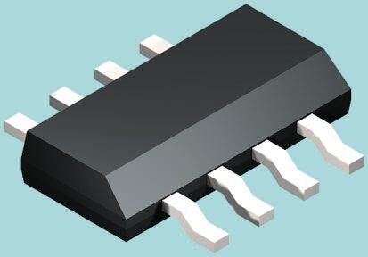
| 描述 | IC BUFF TRPL SCHMIT TRIG SM8缓冲器和线路驱动器 TRIPLE SCHMITT- TRIGGER BUFFER |
| 产品分类 | |
| 品牌 | Texas Instruments |
| 产品手册 | |
| 产品图片 |
|
| rohs | 符合RoHS无铅 / 符合限制有害物质指令(RoHS)规范要求 |
| 产品系列 | 逻辑集成电路,缓冲器和线路驱动器,Texas Instruments SN74LVC3G17DCTR74LVC |
| 数据手册 | |
| 产品型号 | SN74LVC3G17DCTR |
| 产品目录页面 | |
| 产品种类 | 缓冲器和线路驱动器 |
| 传播延迟时间 | 5.4 ns at 3.3 V, 4.1 ns at 5 V |
| 低电平输出电流 | 32 mA |
| 供应商器件封装 | SM8 |
| 元件数 | 3 |
| 其它名称 | 296-16915-1 |
| 包装 | 剪切带 (CT) |
| 单位重量 | 23.400 mg |
| 商标 | Texas Instruments |
| 安装类型 | 表面贴装 |
| 安装风格 | SMD/SMT |
| 封装 | Reel |
| 封装/外壳 | 7-LSSOP(0.11",2.80mm 宽) |
| 封装/箱体 | SSOP-8 |
| 工作温度 | -40°C ~ 125°C |
| 工厂包装数量 | 3000 |
| 最大工作温度 | + 85 C |
| 最小工作温度 | - 40 C |
| 极性 | Non-Inverting |
| 标准包装 | 1 |
| 每元件位数 | 1 |
| 每芯片的通道数量 | 3 |
| 电压-电源 | 1.65 V ~ 5.5 V |
| 电流-输出高,低 | 32mA,32mA |
| 电源电压-最大 | 5.5 V |
| 电源电压-最小 | 1.65 V |
| 系列 | SN74LVC3G17 |
| 输入线路数量 | 3 |
| 输出线路数量 | 3 |
| 逻辑类型 | 施密特触发器 - 缓冲器,驱动器 |
| 逻辑系列 | LVC |
| 高电平输出电流 | - 32 mA |


- 商务部:美国ITC正式对集成电路等产品启动337调查
- 曝三星4nm工艺存在良率问题 高通将骁龙8 Gen1或转产台积电
- 太阳诱电将投资9.5亿元在常州建新厂生产MLCC 预计2023年完工
- 英特尔发布欧洲新工厂建设计划 深化IDM 2.0 战略
- 台积电先进制程称霸业界 有大客户加持明年业绩稳了
- 达到5530亿美元!SIA预计今年全球半导体销售额将创下新高
- 英特尔拟将自动驾驶子公司Mobileye上市 估值或超500亿美元
- 三星加码芯片和SET,合并消费电子和移动部门,撤换高东真等 CEO
- 三星电子宣布重大人事变动 还合并消费电子和移动部门
- 海关总署:前11个月进口集成电路产品价值2.52万亿元 增长14.8%


PDF Datasheet 数据手册内容提取
Product Sample & Technical Tools & Support & Folder Buy Documents Software Community SN74LVC3G17 SCES470F–AUGUST2003–REVISEDAUGUST2015 SN74LVC3G17 Triple Schmitt-Trigger Buffer 1 Features 3 Description • AvailableintheTexasInstruments This triple Schmitt-trigger buffer is designed for 1 1.65-Vto5.5-VV operation. NanoFree™Package CC • Supports5-VV Operation The SN74LVC3G17 device contains three buffers CC and performs the Boolean function Y = A. The device • InputsAcceptVoltagesto5.5V functions as three independent buffers but, because • Maximumt of5.4nsat3.3V pd ofSchmittaction,itmayhavedifferentinputthreshold • LowPowerConsumption,10-μAMaximumI levels for positive-going (V ) and negative-going CC T+ (V )signals. • ±24-mAOutputDriveat3.3V T– • TypicalV (OutputGroundBounce) This device is fully specified for partial-power-down OLP <0.8VatVCC=3.3V,TA=25°C applications using Ioff. The Ioff circuitry disables the outputs, preventing damaging current backflow • TypicalV (OutputV Undershoot) OHV OH throughthedevicewhenitispowereddown. >2VatV =3.3V,T =25°C CC A NanoFree package technology is a major • I SupportsLiveInsertion,Partial-Power-Down off breakthrough in IC packaging concepts, using the die ModeandBackDriveProtection asthepackage. • Latch-UpPerformanceExceeds100mA PerJESD78,ClassII DeviceInformation(1) • ESDProtectionExceedsJESD22 PARTNUMBER PACKAGE BODYSIZE(NOM) – 2000-VHumanBodyModel(A114-A) SN74LVC3G17DCT SSOP(8) 2.95mm×2.80mm – 200-VMachineModel(A115-A) SN74LVC3G17DCU VSSOP(8) 2.30mm×2.00mm – 1000-VCharged-DeviceModel(C101) SN74LVC3G17YZP DSBGA(8) 1.91mm×0.91mm (1) For all available packages, see the orderable addendum at 2 Applications theendofthedatasheet. • AVReceivers • AudioDocks:Portable • Blu-ray®PlayersandHomeTheater • MP3Players/Recorders • PersonalDigitalAssistants(PDAs) • Power:Telecom/ServerAC/DCSupply:Single Controller:AnalogandDigital • SolidStateDrives(SSDs):ClientandEnterprise • TVs:LCD/DigitalandHigh-Definition(HDTVs) • Tablets:Enterprise • VideoAnalytics:Server • WirelessHeadsets,Keyboards,andMice SimplifiedSchematic 1 7 1A 1Y 3 5 2A 2Y 6 2 3A 3Y 1 An IMPORTANT NOTICE at the end of this data sheet addresses availability, warranty, changes, use in safety-critical applications, intellectualpropertymattersandotherimportantdisclaimers.PRODUCTIONDATA.
SN74LVC3G17 SCES470F–AUGUST2003–REVISEDAUGUST2015 www.ti.com Table of Contents 1 Features.................................................................. 1 8.2 FunctionalBlockDiagram.........................................9 2 Applications........................................................... 1 8.3 FeatureDescription...................................................9 3 Description............................................................. 1 8.4 DeviceFunctionalModes..........................................9 4 RevisionHistory..................................................... 2 9 ApplicationandImplementation........................ 10 9.1 ApplicationInformation ..........................................10 5 PinConfigurationandFunctions......................... 3 9.2 TypicalApplication..................................................10 6 Specifications......................................................... 4 10 PowerSupplyRecommendations..................... 11 6.1 AbsoluteMaximumRatings .....................................4 11 Layout................................................................... 11 6.2 ESDRatings..............................................................4 6.3 RecommendedOperatingConditions......................4 11.1 LayoutGuidelines.................................................11 6.4 ThermalInformation..................................................5 11.2 LayoutExample....................................................12 6.5 ElectricalCharacteristics...........................................5 12 DeviceandDocumentationSupport................. 13 6.6 SwitchingCharacteristics..........................................6 12.1 DocumentationSupport........................................13 6.7 OperatingCharacteristics..........................................6 12.2 CommunityResources..........................................13 6.8 TypicalCharacteristics..............................................6 12.3 Trademarks...........................................................13 7 ParameterMeasurementInformation..................7 12.4 ElectrostaticDischargeCaution............................13 12.5 Glossary................................................................13 8 DetailedDescription.............................................. 9 13 Mechanical,Packaging,andOrderable 8.1 Overview...................................................................9 Information........................................................... 13 4 Revision History NOTE:Pagenumbersforpreviousrevisionsmaydifferfrompagenumbersinthecurrentversion. ChangesfromRevisionE(November2013)toRevisionF Page • AddedtheDeviceInformationtable,ESDRatingstable,FeatureDescriptionsection,DeviceFunctionalModes, ApplicationandImplementationsection,PowerSupplyRecommendationssection,Layoutsection,Deviceand DocumentationSupportsection,andMechanical,Packaging,andOrderableInformationsection....................................... 1 • MovedT toAbsoluteMaximumRatingstable..................................................................................................................... 4 stg ChangesfromRevisionD(Feburary2007)toRevisionE Page • UpdateddocumenttonewTIdatasheetformat.................................................................................................................... 1 • Updatedoperatingtemperaturerange................................................................................................................................... 4 2 SubmitDocumentationFeedback Copyright©2003–2015,TexasInstrumentsIncorporated ProductFolderLinks:SN74LVC3G17
SN74LVC3G17 www.ti.com SCES470F–AUGUST2003–REVISEDAUGUST2015 5 Pin Configuration and Functions DCTPackage 8-PinSSOP DCUPackage TopView 8-PinVSSOP TopView 1A 1 8 VCC 1A 1 8 VCC 3Y 2 7 1Y 3Y 2 7 1Y 2A 3 6 3A 2A 3 6 3A GND 4 5 2Y GND 4 5 2Y YZPPackage 8-PinDSBGA BottomView GND 45 2Y 2A 36 3A 3Y 27 1Y 1A 18 VCC Seemechanicaldrawingfordimensions. PinFunctions PIN TYPE DESCRIPTION NAME NO. 1A 1 I Input1 1Y 7 O Output1 2A 3 I Input2 2Y 5 O Output2 3A 6 I Input3 3Y 2 O Output3 GND 4 — Ground V 8 — PowerPin CC Copyright©2003–2015,TexasInstrumentsIncorporated SubmitDocumentationFeedback 3 ProductFolderLinks:SN74LVC3G17
SN74LVC3G17 SCES470F–AUGUST2003–REVISEDAUGUST2015 www.ti.com 6 Specifications 6.1 Absolute Maximum Ratings overoperatingfree-airtemperaturerange(unlessotherwisenoted)(1) MIN MAX UNIT V Supplyvoltage –0.5 6.5 V CC V Inputvoltage(2) –0.5 6.5 V I V Voltageappliedtoanyoutputinthehigh-impedanceorpower-offstate(2) –0.5 6.5 V O V Outputvoltage(2)(3) –0.5 V +0.5 V O CC I Inputclampcurrent V <0 –50 mA IK I I Outputclampcurrent V <0 –50 mA OK O I Continuousoutputcurrent ±50 mA O ContinuouscurrentthroughV orGND ±100 mA CC T Storagetemperature –65 150 °C stg (1) StressesbeyondthoselistedunderAbsoluteMaximumRatingsmaycausepermanentdamagetothedevice.Thesearestressratings only,andfunctionaloperationofthedeviceattheseoranyotherconditionsbeyondthoseindicatedunderRecommendedOperating Conditionsisnotimplied.Exposuretoabsolute-maximum-ratedconditionsforextendedperiodsmayaffectdevicereliability. (2) Theinputnegative-voltageandoutputvoltageratingsmaybeexceedediftheinputandoutputcurrentratingsareobserved. (3) ThevalueofV isprovidedintheRecommendedOperatingConditionstable. CC 6.2 ESD Ratings VALUE UNIT Electrostatic HumanBodyModel(HBM),perANSI/ESDA/JEDECJS-001,allpins(1) +2000 V V ESD discharge Charged-DeviceModel(CDM),perJEDECspecificationJESD22-C101,allpins(2) +1000 (1) JEDECdocumentJEP155statesthat500-VHBMallowssafemanufacturingwithastandardESDcontrolprocess. (2) JEDECdocumentJEP157statesthat250-VCDMallowssafemanufacturingwithastandardESDcontrolprocess. 6.3 Recommended Operating Conditions See (1). MIN MAX UNIT V Supplyvoltage Operating 1.65 5.5 V CC V Inputvoltage 0 5.5 V I V Outputvoltage 0 V V O CC V =1.65V –4 CC V =2.3V –8 CC I High-leveloutputcurrent –16 mA OH V =3V CC –24 V =4.5V –32 CC V =1.65V 4 CC V =2.3V 8 CC I Low-leveloutputcurrent 16 mA OL V =3V CC 24 V =4.5V 32 CC T Operatingfree-airtemperature –40 125 °C A (1) AllunusedinputsofthedevicemustbeheldatV orGNDtoensureproperdeviceoperation.RefertotheTIapplicationreport, CC ImplicationsofSloworFloatingCMOSInputs,SCBA004. 4 SubmitDocumentationFeedback Copyright©2003–2015,TexasInstrumentsIncorporated ProductFolderLinks:SN74LVC3G17
SN74LVC3G17 www.ti.com SCES470F–AUGUST2003–REVISEDAUGUST2015 6.4 Thermal Information SNLVC3G17 THERMALMETRIC(1) DCT(SSOP) DCU(VSSOP) YZP(DSBGA) UNIT 6PINS 6PINS 6PINS R Junction-to-ambientthermalresistance(2) 220 227 102 °C/W θJA (1) Formoreinformationabouttraditionalandnewthermalmetrics,seetheSemiconductorandICPackageThermalMetricsapplication report,SPRA953. (2) ThepackagethermalimpedanceiscalculatedinaccordancewithJESD51-7. 6.5 Electrical Characteristics overrecommendedoperatingfree-airtemperaturerange(unlessotherwisenoted) –40°Cto85°C –40°Cto125°C PARAMETER TESTCONDITIONS VCC MIN TYP(1) MAX MIN TYP(1) MAX UNIT 1.65V 0.79 1.16 0.79 1.16 VT+ 2.3V 1.11 1.56 1.11 1.56 Positive-going 3V 1.5 1.87 1.5 1.87 V inputthreshold voltage 4.5V 2.16 2.74 2.16 2.74 5.5V 2.61 3.33 2.61 3.33 1.65V 0.39 0.62 0.39 0.62 VT– 2.3V 0.58 0.87 0.58 0.87 Negative-going 3V 0.84 1.14 0.84 1.14 V inputthreshold voltage 4.5V 1.41 1.79 1.41 1.79 5.5V 1.87 2.29 1.87 2.29 1.65V 0.37 0.62 0.37 0.62 2.3V 0.48 0.77 0.48 0.77 ΔVT Hysteresis 3V 0.56 0.87 0.56 0.87 V VT+–VT– 4.5V 0.71 1.04 0.71 1.04 5.5V 0.71 1.11 0.71 1.11 IOH=–100μA 1.65Vto5.5V VCC–0.1 VCC–0.1 IOH=–4mA 1.65V 1.2 1.2 IOH=–8mA 2.3V 1.9 1.9 VOH V IOH=–16mA 2.4 2.4 3V IOH=–24mA 2.3 2.3 IOH=–32mA 4.5V 3.8 3.8 IOL=100μA 1.65Vto5.5V 0.1 0.1 IOL=4mA 1.65V 0.45 0.45 IOL=8mA 2.3V 0.3 0.3 VOL V IOL=16mA 0.4 0.4 3V IOL=24mA 0.55 0.75 IOL=32mA 4.5V 0.55 0.75 II VI=5.5VorGND 0to5.5V ±1 ±5 μA Ioff VIorVO=5.5V 0 ±5 ±10 μA ICC VI=5.5VorGND,IO=0 1.65Vto5.5V 10 10 μA ΔICC OOntheerinipnuptuatstVatCVCC–C0o.6rGVN,D 3Vto5.5V 500 500 μA CI VI=VCCorGND 3.3V 4 pF (1) AlltypicalvaluesareatV =3.3V,T =25°C. CC A Copyright©2003–2015,TexasInstrumentsIncorporated SubmitDocumentationFeedback 5 ProductFolderLinks:SN74LVC3G17
SN74LVC3G17 SCES470F–AUGUST2003–REVISEDAUGUST2015 www.ti.com 6.6 Switching Characteristics overrecommendedoperatingfree-airtemperaturerange,C =30pFor50pF(unlessotherwisenoted) L –40°Cto85°C PARAMETER FROM TO TESTCONDITIONS VCC=1.8V VCC=2.5V VCC=3.3V VCC=5V UNIT (INPUT) (OUTPUT) ±0.15V ±0.2V ±0.3V ±0.5V MIN MAX MIN MAX MIN MAX MIN MAX SeeFigure3 4.3 9.2 2 6.2 1.2 5.4 1 4.1 tpd A Y ns SeeFigure3 4.3 10.2 2 7.2 1.2 6.4 1 5.1 6.7 Operating Characteristics T =25°C A V =1.8V V =2.5V V =3.3V V =5V CC CC CC CC PARAMETER TESTCONDITIONS UNIT TYP TYP TYP TYP C Powerdissipationcapacitance f=10MHz 18 19 19 22 pF pd 6.8 Typical Characteristics 10.00 s) n d ( p x t 5.00 a M tpd from A to Y CL= 30 pF or 50 pF -ðì(cid:3)Ù(cid:18)(cid:3)š}(cid:3)íîñÙ(cid:18) 0.00 0.00 1.00 2.00 3.00 4.00 5.00 6.00 Voltage (V) C001 Figure1.MaximumPropagationvsDelayV Voltage CC 6 SubmitDocumentationFeedback Copyright©2003–2015,TexasInstrumentsIncorporated ProductFolderLinks:SN74LVC3G17
SN74LVC3G17 www.ti.com SCES470F–AUGUST2003–REVISEDAUGUST2015 7 Parameter Measurement Information V LOAD R S1 Open From Output L TEST S1 Under Test GND t /t Open C PLH PHL (see NoteA)L RL tPLZ/tPZL VLOAD t /t GND PHZ PZH LOAD CIRCUIT INPUTS V V V C R V CC V t/t M LOAD L L D I r f 1.8 V±0.15 V V £2 ns V /2 2 ×V 15 pF 1 MW 0.15 V CC CC CC 2.5 V±0.2 V V £2 ns V /2 2 ×V 15 pF 1 MW 0.15 V CC CC CC 3.3 V±0.3 V 3 V £2.5 ns 1.5 V 6 V 15 pF 1 MW 0.3 V 5 V±0.5 V V £2.5 ns V /2 2 ×V 15 pF 1 MW 0.3 V CC CC CC V I Timing Input V M 0 V t W VI tsu th V Input V V I M M Data Input V V M M 0 V 0 V VOLTAGE WAVEFORMS VOLTAGE WAVEFORMS PULSE DURATION SETUPAND HOLD TIMES Input VM VM VI COounttpruotl VM VM VI 0 V 0 V t t t t PLH PHL PZL PLZ V Output V /2 Output VM VM OH WSav1e afot rVm 1 VM V + V LOAD VOL (see NoteL OBAD) OL D VOL t t PHL PLH t t PZH PHZ Output VM VM VOH WSa1v eaOfto uGrtmpNu D2t VM VOH–VD VOH VOL (see Note B) »0 V VOLTAGE WAVEFORMS VOLTAGE WAVEFORMS PROPAGATION DELAYTIMES ENABLEAND DISABLE TIMES INVERTINGAND NONINVERTING OUTPUTS LOW-AND HIGH-LEVELENABLING NOTES: A. C includes probe and jig capacitance. L B. Waveform 1 is for an output with internal conditions such that the output is low, except when disabled by the output control. Waveform 2 is for an output with internal conditions such that the output is high, except when disabled by the output control. C. All input pulses are supplied by generators having the following characteristics: PRR£10 MHz, Z = 50W. O D. The outputs are measured one at a time, with one transition per measurement. E. t and t are the same as t . PLZ PHZ dis F. t and t are the same as t . PZL PZH en G.t and t are the same as t . PLH PHL pd H. All parameters and waveforms are not applicable to all devices. Figure2. LoadCircuitandVoltageWaveforms Copyright©2003–2015,TexasInstrumentsIncorporated SubmitDocumentationFeedback 7 ProductFolderLinks:SN74LVC3G17
SN74LVC3G17 SCES470F–AUGUST2003–REVISEDAUGUST2015 www.ti.com Parameter Measurement Information (continued) V LOAD R S1 Open From Output L TEST S1 Under Test GND t /t Open C PLH PHL (see NoteA)L RL tPLZ/tPZL VLOAD t /t GND PHZ PZH LOAD CIRCUIT INPUTS V V V C R V CC V t/t M LOAD L L D I r f 1.8 V±0.15 V V £2 ns V /2 2 ×V 30 pF 1 kW 0.15 V CC CC CC 2.5 V±0.2 V V £2 ns V /2 2 ×V 30 pF 500W 0.15 V CC CC CC 3.3 V±0.3 V 3 V £2.5 ns 1.5 V 6 V 50 pF 500W 0.3 V 5 V±0.5 V V £2.5 ns V /2 2 ×V 50 pF 500W 0.3 V CC CC CC V I Timing Input V M 0 V t W VI tsu th V Input V V I M M Data Input V V M M 0 V 0 V VOLTAGE WAVEFORMS VOLTAGE WAVEFORMS PULSE DURATION SETUPAND HOLD TIMES Input VM VM VI COounttpruotl VM VM VI 0 V 0 V t t t t PLH PHL PZL PLZ V Output V /2 Output VM VM OH WSav1e afot rVm 1 VM V + V LOAD VOL (see NoteL OBAD) OL D VOL t t PHL PLH t t PZH PHZ Output VM VM VOH WSa1v eaOfto uGrtmpNu D2t VM VOH–VD VOH VOL (see Note B) »0 V VOLTAGE WAVEFORMS VOLTAGE WAVEFORMS PROPAGATION DELAYTIMES ENABLEAND DISABLE TIMES INVERTINGAND NONINVERTING OUTPUTS LOW-AND HIGH-LEVELENABLING NOTES: A. C includes probe and jig capacitance. L B. Waveform 1 is for an output with internal conditions such that the output is low, except when disabled by the output control. Waveform 2 is for an output with internal conditions such that the output is high, except when disabled by the output control. C. All input pulses are supplied by generators having the following characteristics: PRR£10 MHz, Z = 50W. O D. The outputs are measured one at a time, with one transition per measurement. E. t and t are the same as t . PLZ PHZ dis F. t and t are the same as t . PZL PZH en G.t and t are the same as t . PLH PHL pd H. All parameters and waveforms are not applicable to all devices. Figure3. LoadCircuitandVoltageWaveforms 8 SubmitDocumentationFeedback Copyright©2003–2015,TexasInstrumentsIncorporated ProductFolderLinks:SN74LVC3G17
SN74LVC3G17 www.ti.com SCES470F–AUGUST2003–REVISEDAUGUST2015 8 Detailed Description 8.1 Overview This triple Schmitt-trigger buffer is designed for 1.65-V to 5.5-V V operation. The SN74LVC3G17 device CC contains three buffers and performs the Boolean function Y = A. The device functions as three independent buffers but, because of Schmitt action, it may have different input threshold levels for positive-going (V ) and T+ negative-going (V ) signals. This device is fully specified for partial-power-down applications using I . The I T– off off circuitry disables the outputs, preventing damaging current backflow through the device when it is powered down. NanoFree™ package technology is a major breakthrough in IC packaging concepts, using the die as the package. 8.2 Functional Block Diagram 1 7 1A 1Y 3 5 2A 2Y 6 2 3A 3Y 8.3 Feature Description SN74LVC3G17 is available in NanoFree package. NanoFree is a major breakthrough in IC packaging concepts, it is a bare die package developed for applications that require the smallest possible package. The device supports5-VV Operation.AllInputsacceptvoltagesupto5.5V. ±24-mAOutputDriveat3.3V.Themaximum CC time propagation delay (t ) is 5.4 ns at 3.3 V. Low Power Consumption, 10-μA Max I . Typical output ground pd CC bounce (V ) and Output V Undershoot (V ). This device is fully specified for partial-powerdown OLP OH OHV applications using I . The I feature ensures that damaging current will not backflow through the device when it off off is powered down. The SN74LVC3G17 device has isolation during power off. I supports live insertion, partial- off power-down mode and back drive protection. The device is latch-up resistant with 100 mA exceeding the JESD 78 standard, class II, providing protection from destruction due to latch-up. This device is protected against electrostatic discharge. It is tested per JESD 22 using 2000-V human-body model (A114-B), 200-V machine model(A115-A),and1000-Vcharged-devicemodel(C101). 8.4 Device Functional Modes Table1liststhefunctionalmodesoftheSN74LVC3G17. Table1.FunctionTable INPUT OUTPUT A Y H H L L Copyright©2003–2015,TexasInstrumentsIncorporated SubmitDocumentationFeedback 9 ProductFolderLinks:SN74LVC3G17
SN74LVC3G17 SCES470F–AUGUST2003–REVISEDAUGUST2015 www.ti.com 9 Application and Implementation NOTE Information in the following applications sections is not part of the TI component specification, and TI does not warrant its accuracy or completeness. TI’s customers are responsible for determining suitability of components for their purposes. Customers should validateandtesttheirdesignimplementationtoconfirmsystemfunctionality. 9.1 Application Information TheSN74LVC3G17devicecontainsthreebuffersandperformstheBooleanfunctionY=A.Thedevicefunctions as three independent buffers, but because of Schmitt action, it may have different input threshold levels for positive-going (V ) and negative-going (V ) signals. In this application, the engineer chooses to use just a T+ T– singleSchmittTriggerbuffer.Inthiscase,theothertwoinputsshouldbetiedtoVCCorGND. 9.2 Typical Application 3 Device Figure4. DevicePowerButtonCircuit 9.2.1 DesignRequirements This device uses CMOS technology and has balanced output drive. Care should be taken to avoid bus contention because it can drive currents that would exceed maximum limits. Outputs can be combined to producehigherdrivebutthehighdrivewillalsocreatefasteredgesintolightloadssoroutingandloadconditions shouldbeconsideredtopreventringing. 9.2.2 DetailedDesignProcedure 1. RecommendedInputConditions: – Forspecifiedhighandlowlevels,see(V andV )inRecommendedOperatingConditions table. IH IL – Inputsareovervoltagetolerantallowingthemtogoashighas5.5VatanyvalidV . CC 2. RecommendOutputConditions: – Loadcurrentsshouldnotexceed50mAperoutputand100mAtotalforthepart. – Series resistors on the output may be used if the user desires to slow the output edge signal or limit the outputcurrent. 10 SubmitDocumentationFeedback Copyright©2003–2015,TexasInstrumentsIncorporated ProductFolderLinks:SN74LVC3G17
SN74LVC3G17 www.ti.com SCES470F–AUGUST2003–REVISEDAUGUST2015 Typical Application (continued) 9.2.3 ApplicationCurves 60 100 TA=25°C,VCC=3V, TA=25°C,VCC=3V, 40 VIH=3V,VIL=0V, VIH=3V,VIL=0V, AllOutputsSwitching 80 AllOutputsSwitching 20 60 0 A A m m – –20 – 40 OH OL I I –40 20 –60 0 –80 –100 –20 –1 –0.5 0.0 0.5 1.0 1.5 2.0 2.5 3.0 3.5 4.0 –0.2 0.0 0.2 0.4 0.6 0.8 1.0 1.2 1.4 1.6 VOH–V VOL–V Figure5.OutputCurrentDrive Figure6.OutputCurrentDrive vsHIGH-levelOutputVoltage vsLOW-levelOutputVoltage 10 Power Supply Recommendations The power supply can be any voltage between the minimum and maximum supply voltage rating located in the AbsoluteMaximumRatingstable. Each V terminal should have a good bypass capacitor to prevent power disturbance. For devices with a single CC supply, a 0.1-μF capacitor is recommended. If there are multiple V terminals then 0.01-μF or 0.022-μF CC capacitors are recommended for each power terminal. It is ok to parallel multiple bypass capacitors to reject different frequencies of noise. Multiple bypass capacitors may be paralleled to reject different frequencies of noise.Thebypasscapacitorshouldbeinstalledasclosetothepowerterminalaspossibleforthebestresults. 11 Layout 11.1 Layout Guidelines When using multiple bit logic devices, inputs should not float. In many cases, functions or parts of functions of digital logic devices are unused. Some examples are when only two inputs of a triple-input AND gate are used, or when only 3 of the 4-buffer gates are used. Such input pins should not be left unconnected because the undefinedvoltagesattheoutsideconnectionsresultinundefinedoperationalstates. Specified in Figure 7 are rules that must be observed under all circumstances. All unused inputs of digital logic devices must be connected to a high or low bias to prevent them from floating. The logic level that should be applied to any particular unused input depends on the function of the device. Generally they will be tied to GND orV ,whichevermakesmoresenseorismoreconvenient. CC Copyright©2003–2015,TexasInstrumentsIncorporated SubmitDocumentationFeedback 11 ProductFolderLinks:SN74LVC3G17
SN74LVC3G17 SCES470F–AUGUST2003–REVISEDAUGUST2015 www.ti.com 11.2 Layout Example VCC Input Unused Input Output Unused Input Output Input Figure7. LayoutDiagram 12 SubmitDocumentationFeedback Copyright©2003–2015,TexasInstrumentsIncorporated ProductFolderLinks:SN74LVC3G17
SN74LVC3G17 www.ti.com SCES470F–AUGUST2003–REVISEDAUGUST2015 12 Device and Documentation Support 12.1 Documentation Support 12.1.1 RelatedDocumentation Forrelateddocumentation,seethefollowing: ImplicationsofSloworFloatingCMOSInputs,SCBA004 12.2 Community Resources The following links connect to TI community resources. Linked contents are provided "AS IS" by the respective contributors. They do not constitute TI specifications and do not necessarily reflect TI's views; see TI's Terms of Use. TIE2E™OnlineCommunity TI'sEngineer-to-Engineer(E2E)Community.Createdtofostercollaboration amongengineers.Ate2e.ti.com,youcanaskquestions,shareknowledge,exploreideasandhelp solveproblemswithfellowengineers. DesignSupport TI'sDesignSupport QuicklyfindhelpfulE2Eforumsalongwithdesignsupporttoolsand contactinformationfortechnicalsupport. 12.3 Trademarks E2EisatrademarkofTexasInstruments. Blu-rayisaregisteredtrademarkofBlu-rayDiscAssociation. NanoFreeisatrademarkofTexasInsturments. Allothertrademarksarethepropertyoftheirrespectiveowners. 12.4 Electrostatic Discharge Caution Thesedeviceshavelimitedbuilt-inESDprotection.Theleadsshouldbeshortedtogetherorthedeviceplacedinconductivefoam duringstorageorhandlingtopreventelectrostaticdamagetotheMOSgates. 12.5 Glossary SLYZ022—TIGlossary. Thisglossarylistsandexplainsterms,acronyms,anddefinitions. 13 Mechanical, Packaging, and Orderable Information The following pages include mechanical packaging and orderable information. This information is the most current data available for the designated devices. This data is subject to change without notice and revision of thisdocument.Forbrowserbasedversionsofthisdatasheet,refertothelefthandnavigation. Copyright©2003–2015,TexasInstrumentsIncorporated SubmitDocumentationFeedback 13 ProductFolderLinks:SN74LVC3G17
PACKAGE OPTION ADDENDUM www.ti.com 6-Feb-2020 PACKAGING INFORMATION Orderable Device Status Package Type Package Pins Package Eco Plan Lead/Ball Finish MSL Peak Temp Op Temp (°C) Device Marking Samples (1) Drawing Qty (2) (6) (3) (4/5) SN74LVC3G17DCTR ACTIVE SM8 DCT 8 3000 Green (RoHS NIPDAU Level-1-260C-UNLIM -40 to 125 C17 & no Sb/Br) (R, Z) SN74LVC3G17DCTRE4 ACTIVE SM8 DCT 8 3000 Green (RoHS NIPDAU Level-1-260C-UNLIM -40 to 125 C17 & no Sb/Br) (R, Z) SN74LVC3G17DCTRG4 ACTIVE SM8 DCT 8 3000 Green (RoHS NIPDAU Level-1-260C-UNLIM -40 to 125 C17 & no Sb/Br) (R, Z) SN74LVC3G17DCUR ACTIVE VSSOP DCU 8 3000 Green (RoHS NIPDAU | SN Level-1-260C-UNLIM -40 to 125 (17, C17Q, C17R) & no Sb/Br) CZ SN74LVC3G17DCURG4 ACTIVE VSSOP DCU 8 3000 Green (RoHS NIPDAU Level-1-260C-UNLIM -40 to 125 C17R & no Sb/Br) SN74LVC3G17YZPR ACTIVE DSBGA YZP 8 3000 Green (RoHS SNAGCU Level-1-260C-UNLIM -40 to 85 C7N & no Sb/Br) (1) The marketing status values are defined as follows: ACTIVE: Product device recommended for new designs. LIFEBUY: TI has announced that the device will be discontinued, and a lifetime-buy period is in effect. NRND: Not recommended for new designs. Device is in production to support existing customers, but TI does not recommend using this part in a new design. PREVIEW: Device has been announced but is not in production. Samples may or may not be available. OBSOLETE: TI has discontinued the production of the device. (2) RoHS: TI defines "RoHS" to mean semiconductor products that are compliant with the current EU RoHS requirements for all 10 RoHS substances, including the requirement that RoHS substance do not exceed 0.1% by weight in homogeneous materials. Where designed to be soldered at high temperatures, "RoHS" products are suitable for use in specified lead-free processes. TI may reference these types of products as "Pb-Free". RoHS Exempt: TI defines "RoHS Exempt" to mean products that contain lead but are compliant with EU RoHS pursuant to a specific EU RoHS exemption. Green: TI defines "Green" to mean the content of Chlorine (Cl) and Bromine (Br) based flame retardants meet JS709B low halogen requirements of <=1000ppm threshold. Antimony trioxide based flame retardants must also meet the <=1000ppm threshold requirement. (3) MSL, Peak Temp. - The Moisture Sensitivity Level rating according to the JEDEC industry standard classifications, and peak solder temperature. (4) There may be additional marking, which relates to the logo, the lot trace code information, or the environmental category on the device. (5) Multiple Device Markings will be inside parentheses. Only one Device Marking contained in parentheses and separated by a "~" will appear on a device. If a line is indented then it is a continuation of the previous line and the two combined represent the entire Device Marking for that device. Addendum-Page 1
PACKAGE OPTION ADDENDUM www.ti.com 6-Feb-2020 (6) Lead/Ball Finish - Orderable Devices may have multiple material finish options. Finish options are separated by a vertical ruled line. Lead/Ball Finish values may wrap to two lines if the finish value exceeds the maximum column width. Important Information and Disclaimer:The information provided on this page represents TI's knowledge and belief as of the date that it is provided. TI bases its knowledge and belief on information provided by third parties, and makes no representation or warranty as to the accuracy of such information. Efforts are underway to better integrate information from third parties. TI has taken and continues to take reasonable steps to provide representative and accurate information but may not have conducted destructive testing or chemical analysis on incoming materials and chemicals. TI and TI suppliers consider certain information to be proprietary, and thus CAS numbers and other limited information may not be available for release. In no event shall TI's liability arising out of such information exceed the total purchase price of the TI part(s) at issue in this document sold by TI to Customer on an annual basis. Addendum-Page 2
PACKAGE MATERIALS INFORMATION www.ti.com 17-Apr-2020 TAPE AND REEL INFORMATION *Alldimensionsarenominal Device Package Package Pins SPQ Reel Reel A0 B0 K0 P1 W Pin1 Type Drawing Diameter Width (mm) (mm) (mm) (mm) (mm) Quadrant (mm) W1(mm) SN74LVC3G17DCTR SM8 DCT 8 3000 180.0 13.0 3.35 4.5 1.55 4.0 12.0 Q3 SN74LVC3G17DCUR VSSOP DCU 8 3000 178.0 9.5 2.25 3.35 1.05 4.0 8.0 Q3 SN74LVC3G17DCUR VSSOP DCU 8 3000 180.0 8.4 2.25 3.35 1.05 4.0 8.0 Q3 SN74LVC3G17DCUR VSSOP DCU 8 3000 180.0 9.0 2.05 3.3 1.0 4.0 8.0 Q3 SN74LVC3G17DCURG4 VSSOP DCU 8 3000 180.0 8.4 2.25 3.35 1.05 4.0 8.0 Q3 SN74LVC3G17YZPR DSBGA YZP 8 3000 178.0 9.2 1.02 2.02 0.63 4.0 8.0 Q1 PackMaterials-Page1
PACKAGE MATERIALS INFORMATION www.ti.com 17-Apr-2020 *Alldimensionsarenominal Device PackageType PackageDrawing Pins SPQ Length(mm) Width(mm) Height(mm) SN74LVC3G17DCTR SM8 DCT 8 3000 182.0 182.0 20.0 SN74LVC3G17DCUR VSSOP DCU 8 3000 202.0 201.0 28.0 SN74LVC3G17DCUR VSSOP DCU 8 3000 202.0 201.0 28.0 SN74LVC3G17DCUR VSSOP DCU 8 3000 182.0 182.0 20.0 SN74LVC3G17DCURG4 VSSOP DCU 8 3000 202.0 201.0 28.0 SN74LVC3G17YZPR DSBGA YZP 8 3000 220.0 220.0 35.0 PackMaterials-Page2
MECHANICAL DATA MPDS049B – MAY 1999 – REVISED OCTOBER 2002 DCT (R-PDSO-G8) PLASTIC SMALL-OUTLINE PACKAGE 0,30 0,65 0,13 M 0,15 8 5 0,15 NOM 2,90 4,25 ÇÇÇÇÇ 2,70 3,75 ÇÇÇÇÇ ÇÇÇÇÇ Gage Plane ÇÇÇÇÇ PIN 1 INDEX AREA 0,25 1 4 0°– 8° 3,15 0,60 2,75 0,20 1,30 MAX Seating Plane 0,10 0,10 0,00 4188781/C 09/02 NOTES: A. All linear dimensions are in millimeters. B. This drawing is subject to change without notice. C. Body dimensions do not include mold flash or protrusion D. Falls within JEDEC MO-187 variation DA. • POST OFFICE BOX 655303 DALLAS, TEXAS 75265
None
PACKAGE OUTLINE YZP0008 DSBGA - 0.5 mm max height SCALE 8.000 DIE SIZE BALL GRID ARRAY B E A BALL A1 CORNER D C 0.5 MAX SEATING PLANE 0.19 0.05 C 0.15 BALL TYP 0.5 TYP D C SYMM 1.5 D: Max = 1.919 mm, Min =1 .858 mm TYP B E: Max = 0.918 mm, Min =0 .857 mm 0.5 TYP A 0.25 8X 1 2 0.21 0.015 C A B SYMM 4223082/A 07/2016 NOTES: 1. All linear dimensions are in millimeters. Any dimensions in parenthesis are for reference only. Dimensioning and tolerancing per ASME Y14.5M. 2. This drawing is subject to change without notice. www.ti.com
EXAMPLE BOARD LAYOUT YZP0008 DSBGA - 0.5 mm max height DIE SIZE BALL GRID ARRAY (0.5) TYP 8X ( 0.23) 1 2 A (0.5) TYP B SYMM C D SYMM LAND PATTERN EXAMPLE SCALE:40X SOLDER MASK 0.05 MAX 0.05 MIN ( 0.23) OPENING SOLDER MASK OPENING ( 0.23) METAL METAL UNDER SOLDER MASK NON-SOLDER MASK SOLDER MASK DEFINED DEFINED (PREFERRED) SOLDER MASK DETAILS NOT TO SCALE 4223082/A 07/2016 NOTES: (continued) 3. Final dimensions may vary due to manufacturing tolerance considerations and also routing constraints. For more information, see Texas Instruments literature number SNVA009 (www.ti.com/lit/snva009). www.ti.com
EXAMPLE STENCIL DESIGN YZP0008 DSBGA - 0.5 mm max height DIE SIZE BALL GRID ARRAY (0.5) TYP 8X ( 0.25) (R0.05) TYP 1 2 A (0.5) TYP B SYMM C METAL TYP D SYMM SOLDER PASTE EXAMPLE BASED ON 0.1 mm THICK STENCIL SCALE:40X 4223082/A 07/2016 NOTES: (continued) 4. Laser cutting apertures with trapezoidal walls and rounded corners may offer better paste release. www.ti.com
None
None
IMPORTANTNOTICEANDDISCLAIMER TI PROVIDES TECHNICAL AND RELIABILITY DATA (INCLUDING DATASHEETS), DESIGN RESOURCES (INCLUDING REFERENCE DESIGNS), APPLICATION OR OTHER DESIGN ADVICE, WEB TOOLS, SAFETY INFORMATION, AND OTHER RESOURCES “AS IS” AND WITH ALL FAULTS, AND DISCLAIMS ALL WARRANTIES, EXPRESS AND IMPLIED, INCLUDING WITHOUT LIMITATION ANY IMPLIED WARRANTIES OF MERCHANTABILITY, FITNESS FOR A PARTICULAR PURPOSE OR NON-INFRINGEMENT OF THIRD PARTY INTELLECTUAL PROPERTY RIGHTS. These resources are intended for skilled developers designing with TI products. You are solely responsible for (1) selecting the appropriate TI products for your application, (2) designing, validating and testing your application, and (3) ensuring your application meets applicable standards, and any other safety, security, or other requirements. These resources are subject to change without notice. TI grants you permission to use these resources only for development of an application that uses the TI products described in the resource. Other reproduction and display of these resources is prohibited. No license is granted to any other TI intellectual property right or to any third party intellectual property right. TI disclaims responsibility for, and you will fully indemnify TI and its representatives against, any claims, damages, costs, losses, and liabilities arising out of your use of these resources. TI’s products are provided subject to TI’s Terms of Sale (www.ti.com/legal/termsofsale.html) or other applicable terms available either on ti.com or provided in conjunction with such TI products. TI’s provision of these resources does not expand or otherwise alter TI’s applicable warranties or warranty disclaimers for TI products. Mailing Address: Texas Instruments, Post Office Box 655303, Dallas, Texas 75265 Copyright © 2020, Texas Instruments Incorporated