ICGOO在线商城 > 集成电路(IC) > 逻辑 - 缓冲器,驱动器,接收器,收发器 > SN74LVC3G07DCUR
 Datasheet下载
- 型号: SN74LVC3G07DCUR
- 制造商: Texas Instruments
- 库位|库存: xxxx|xxxx
- 要求:
| 数量阶梯 | 香港交货 | 国内含税 |
| +xxxx | $xxxx | ¥xxxx |
查看当月历史价格
查看今年历史价格
SN74LVC3G07DCUR产品简介:
ICGOO电子元器件商城为您提供SN74LVC3G07DCUR由Texas Instruments设计生产,在icgoo商城现货销售,并且可以通过原厂、代理商等渠道进行代购。 SN74LVC3G07DCUR价格参考¥1.72-¥2.15。Texas InstrumentsSN74LVC3G07DCUR封装/规格:逻辑 - 缓冲器,驱动器,接收器,收发器, Buffer, Non-Inverting 3 Element 1 Bit per Element Open Drain Output US8。您可以下载SN74LVC3G07DCUR参考资料、Datasheet数据手册功能说明书,资料中有SN74LVC3G07DCUR 详细功能的应用电路图电压和使用方法及教程。
SN74LVC3G07DCUR 是由 Texas Instruments(德州仪器)生产的一款逻辑缓冲器,属于 SN74LVC 系列,采用 14 引脚的小型封装。它主要用于信号传输和电平转换的场景,具有低功耗、高稳定性和宽电压范围(1.65V 至 5.5V)的特点,适用于各种数字电路设计。以下是该型号的一些典型应用场景:

 1. 信号增强与驱动
   - 在多负载系统中,当微控制器或 FPGA 的输出信号不足以驱动多个输入端时,SN74LVC3G07DCUR 可以作为缓冲器增强信号强度,确保信号完整性。
   - 用于驱动 LED 指示灯、继电器或其他需要较高电流的设备。

 2. 电平转换
   - 由于其支持宽电压范围,可以实现不同电压逻辑系统的电平转换。例如,在 3.3V 和 5V 系统之间进行信号传递时,该芯片可以确保兼容性。

 3. 数据总线扩展
   - 在多设备共享数据总线的场景中,使用缓冲器可以隔离各个设备,减少信号干扰,提高系统稳定性。
   - 常见于计算机主板、嵌入式系统或工业控制设备中。

 4. 时钟信号分配
   - 在需要将单一时钟信号分发到多个模块的场景中,SN74LVC3G07DCUR 可以提供干净且同步的时钟信号,避免信号衰减或失真。

 5. 通信接口设计
   - 在 UART、SPI 或 I2C 等通信协议中,缓冲器可用于增强信号传输距离或隔离主从设备,防止信号过载或损坏。

 6. 消费电子与家电
   - 应用于电视、音响、打印机等消费电子产品中,处理内部信号传输或接口扩展。
   - 在家用电器(如空调、冰箱)中,用于控制面板与主控板之间的信号传递。

 7. 工业自动化
   - 在工业控制系统中,用于传感器信号采集、PLC 输入/输出扩展或人机界面信号处理。

 总结
SN74LVC3G07DCUR 的主要优势在于其低功耗、高性能和广泛的电压适应性,适合各种需要信号缓冲、驱动或电平转换的应用场景。无论是消费电子、通信设备还是工业控制领域,这款芯片都能提供可靠的解决方案。
| 参数 | 数值 |
| 产品目录 | 集成电路 (IC)半导体 |
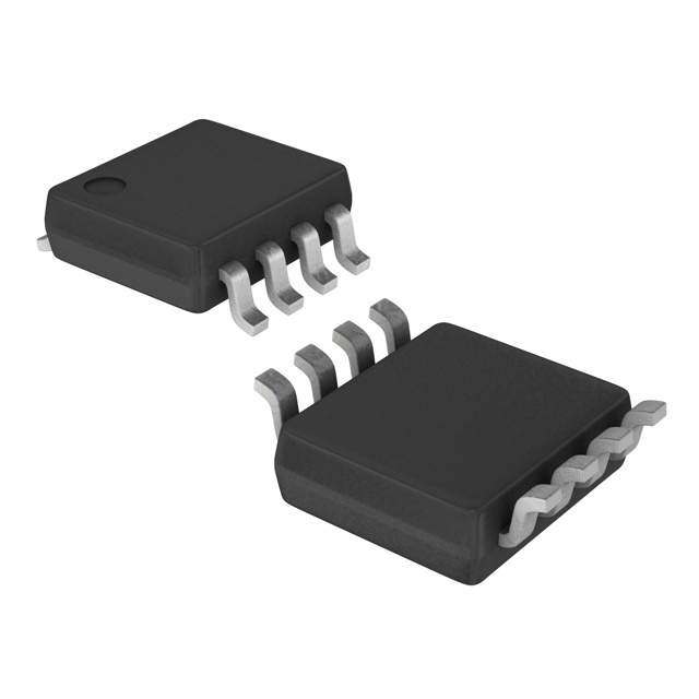
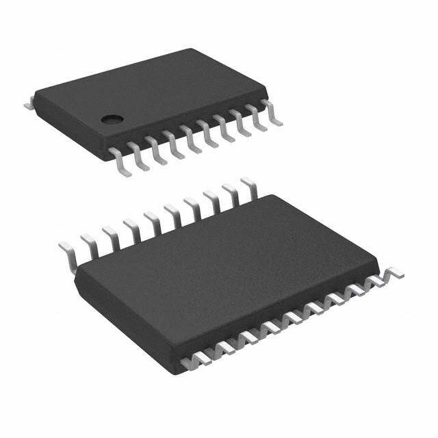
| 描述 | IC BUFF/DVR TRPL N-INV US8缓冲器和线路驱动器 Triple w/ OD |
| 产品分类 | |
| 品牌 | Texas Instruments |
| 产品手册 | http://www.ti.com/lit/gpn/sn74lvc3g07 |
| 产品图片 |
|
| rohs | 符合RoHS无铅 / 符合限制有害物质指令(RoHS)规范要求 |
| 产品系列 | 逻辑集成电路,缓冲器和线路驱动器,Texas Instruments SN74LVC3G07DCUR74LVC |
| 数据手册 | |
| 产品型号 | SN74LVC3G07DCUR |
| 产品目录页面 | |
| 产品种类 | 缓冲器和线路驱动器 |
| 传播延迟时间 | 3.7 ns at 3.3 V, 2.9 ns at 5 V |
| 低电平输出电流 | 32 mA |
| 供应商器件封装 | US8 |
| 元件数 | 3 |
| 其它名称 | 296-13283-1 |
| 包装 | 剪切带 (CT) |
| 单位重量 | 9.600 mg |
| 商标 | Texas Instruments |
| 安装类型 | 表面贴装 |
| 安装风格 | SMD/SMT |
| 封装 | Reel |
| 封装/外壳 | 8-VFSOP(0.091",2.30mm 宽) |
| 封装/箱体 | VSSOP-8 |
| 工作温度 | -40°C ~ 125°C |
| 工厂包装数量 | 3000 |
| 最大工作温度 | + 80 C |
| 最小工作温度 | - 45 C |
| 极性 | Non-Inverting |
| 标准包装 | 1 |
| 每元件位数 | 1 |
| 每芯片的通道数量 | 3 |
| 电压-电源 | 1.65 V ~ 5.5 V |
| 电流-输出高,低 | -,32mA |
| 电源电压-最大 | 5.5 V |
| 电源电压-最小 | 1.65 V |
| 系列 | SN74LVC3G07 |
| 输入线路数量 | 3 |
| 输出类型 | Open Drain |
| 输出线路数量 | 3 |
| 逻辑类型 | 缓冲器/线路驱动器,非反相并带开漏极 |
| 逻辑系列 | LVC |


- 商务部:美国ITC正式对集成电路等产品启动337调查
- 曝三星4nm工艺存在良率问题 高通将骁龙8 Gen1或转产台积电
- 太阳诱电将投资9.5亿元在常州建新厂生产MLCC 预计2023年完工
- 英特尔发布欧洲新工厂建设计划 深化IDM 2.0 战略
- 台积电先进制程称霸业界 有大客户加持明年业绩稳了
- 达到5530亿美元!SIA预计今年全球半导体销售额将创下新高
- 英特尔拟将自动驾驶子公司Mobileye上市 估值或超500亿美元
- 三星加码芯片和SET,合并消费电子和移动部门,撤换高东真等 CEO
- 三星电子宣布重大人事变动 还合并消费电子和移动部门
- 海关总署:前11个月进口集成电路产品价值2.52万亿元 增长14.8%


PDF Datasheet 数据手册内容提取
SN74LVC3G07 www.ti.com SCES365K–AUGUST2001–REVISEDNOVEMBER2013 Triple Buffer/Driver With Open-drain Outputs CheckforSamples:SN74LVC3G07 FEATURES DESCRIPTION 1 • AvailableintheTexasInstruments NanoFree™ This triple buffer/driver is designed for 1.65-V to 5.5-V 2 V operation. Package CC • Supports5-VV Operation NanoFree™ package technology is a major CC breakthrough in IC packaging concepts, using the die • Maxt of3.7nsat3.3V pd asthepackage. • LowPowerConsumption,10-μAMaxI CC The output of the SN74LVC3G07 is open drain and • ±24-mAOutputDriveat3.3V can be connected to other open-drain outputs to • InputandOpen-DrainOutputAccepts implement active-low wired-OR or active-high wired- Voltagesupto5.5V ANDfunctions.Themaximumsinkcurrentis32mA. • TypicalV (OutputGroundBounce) <0.8Vat OLP This device is fully specified for partial-power-down VCC=3.3V,TA=25°C applications using Ioff. The Ioff circuitry disables the • TypicalV (OutputV Undershoot) >2Vat outputs, preventing damaging current backflow OHV OH V =3.3V,T =25°C throughthedevicewhenitispowereddown. CC A • I SupportsLiveInsertion,Partial-Power- off DownModeandBackDriveProtection • Latch-UpPerformanceExceeds100mAPer JESD78,ClassII • ESDProtectionExceedsJESD22 – 2000-VHuman-BodyModel(A114-A) – 200-VMachineModel(A115-A) – 1000-VCharged-DeviceModel(C101) DCT PACKAGE DCU PACKAGE YZP PACKAGE (TOP VIEW) (TOP VIEW) (BOTTOM VIEW) 1A 1 8 VCC 1A 1 8 VCC GN2AD 3456 23YA 3Y 2 7 1Y 3Y 27 1Y 3Y 2 7 1Y 2A 3 6 3A 1A 18 VCC GND 4 5 2Y 2A 3 6 3A GND 4 5 2Y See mechanical drawings for dimensions. 1 Pleasebeawarethatanimportantnoticeconcerningavailability,standardwarranty,anduseincriticalapplicationsof TexasInstrumentssemiconductorproductsanddisclaimerstheretoappearsattheendofthisdatasheet. NanoFreeisatrademarkofTexasInstruments. 2 PRODUCTIONDATAinformationiscurrentasofpublicationdate. Copyright©2001–2013,TexasInstrumentsIncorporated Products conform to specifications per the terms of the Texas Instruments standard warranty. Production processing does not necessarilyincludetestingofallparameters.
SN74LVC3G07 SCES365K–AUGUST2001–REVISEDNOVEMBER2013 www.ti.com FunctionTable (EachBuffer/Driver) INPUT OUTPUT A Y H H L L LOGIC DIAGRAM (POSITIVE LOGIC) 1 7 1A 1Y 3 5 2A 2Y 6 2 3A 3Y Absolute Maximum Ratings(1) overoperatingfree-airtemperaturerange(unlessotherwisenoted) MIN MAX UNIT V Supplyvoltagerange –0.5 6.5 V CC V Inputvoltagerange(2) –0.5 6.5 V I V Voltagerangeappliedtoanyoutputinthehigh-impedanceorpower-offstate(2) –0.5 6.5 V O V Voltagerangeappliedtoanyoutputinthehighorlowstate(2) (3) –0.5 6.5 V O I Inputclampcurrent V <0 –50 mA IK I I Outputclampcurrent V <0 –50 mA OK O I Continuousoutputcurrent ±50 mA O ContinuouscurrentthroughV orGND ±100 mA CC DCTpackage 220 θ Packagethermalimpedance(4) DCUpackage 227 °C/W JA YZPpackage 102 T Storagetemperaturerange –65 150 °C stg (1) Stressesbeyondthoselistedunder"absolutemaximumratings"maycausepermanentdamagetothedevice.Thesearestressratings only,andfunctionaloperationofthedeviceattheseoranyotherconditionsbeyondthoseindicatedunder"recommendedoperating conditions"isnotimplied.Exposuretoabsolute-maximum-ratedconditionsforextendedperiodsmayaffectdevicereliability. (2) Theinputnegative-voltageandoutputvoltageratingsmaybeexceedediftheinputandoutputclamp-currentratingsareobserved. (3) ThevalueofV isprovidedintherecommendedoperatingconditionstable. CC (4) ThepackagethermalimpedanceiscalculatedinaccordancewithJESD51-7. 2 SubmitDocumentationFeedback Copyright©2001–2013,TexasInstrumentsIncorporated ProductFolderLinks:SN74LVC3G07
SN74LVC3G07 www.ti.com SCES365K–AUGUST2001–REVISEDNOVEMBER2013 Recommended Operating Conditions(1) MIN MAX UNIT Operating 1.65 5.5 VCC Supplyvoltage V Dataretentiononly 1.5 VCC=1.65Vto1.95V 0.65×VCC VCC=2.3Vto2.7V 1.7 VIH High-levelinputvoltage V VCC=3Vto3.6V 2 VCC=4.5Vto5.5V 0.7×VCC VCC=1.65Vto1.95V 0.35×VCC VCC=2.3Vto2.7V 0.7 VIL Low-levelinputvoltage V VCC=3Vto3.6V 0.8 VCC=4.5Vto5.5V 0.3×VCC VI Inputvoltage 0 5.5 V VO Outputvoltage 0 5.5 V VCC=1.65V 4 VCC=2.3V 8 IOL Low-leveloutputcurrent 16 mA VCC=3V 24 VCC=4.5V 32 VCC=1.8V±0.15V,2.5V±0.2V 20 Δt/Δv Inputtransitionriseorfallrate VCC=3.3V±0.3V 10 ns/V VCC=5V±0.5V 5 TA Operatingfree-airtemperature –40 125 °C (1) AllunusedinputsofthedevicemustbeheldatV orGNDtoensureproperdeviceoperation.RefertotheTIapplicationreport, CC ImplicationsofSloworFloatingCMOSInputs,literaturenumberSCBA004. Electrical Characteristics overrecommendedoperatingfree-airtemperaturerange(unlessotherwisenoted) –40°Cto85°C –40°Cto125°C PARAMETER TESTCONDITIONS VCC MIN TYP(1) MAX MIN TYP(1) MAX UNIT 1.65Vto5.5 IOL=100μA V 0.1 0.1 IOL=4mA 1.65V 0.45 0.45 VOL IOL=8mA 2.3V 0.3 0.3 V IOL=16mA 0.4 0.4 3V IOL=24mA 0.55 0.75 IOL=32mA 4.5V 0.55 0.75 II Ainputs VI=5.5VorGND 0to5.5V ±5 ±5 μA Ioff VIorVO=5.5V 0 ±10 ±10 μA 1.65Vto5.5 ICC VI=5.5VorGND, IO=0 V 10 10 μA ΔICC OneinputatVCC–0.6V, OtherinputsatVCCorGND 3Vto5.5V 500 500 μA CI VI=VCCorGND 3.3V 3.5 3.5 pF (1) AlltypicalvaluesareatV =3.3V,T =25°C. CC A Switching Characteristics overrecommendedoperatingfree-airtemperaturerange(unlessotherwisenoted)(seeFigure1) SN74LVC3G07 –40°Cto85°C FROM TO PARAMETER (INPUT) (OUTPUT) VCC=1.8V VCC=2.5V VCC=3.3V VCC=5V UNIT ±0.15V ±0.2V ±0.3V ±0.5V MIN MAX MIN MAX MIN MAX MIN MAX tpd A Y 1.5 7.8 1 4.3 1.1 3.7 1 2.9 ns Copyright©2001–2013,TexasInstrumentsIncorporated SubmitDocumentationFeedback 3 ProductFolderLinks:SN74LVC3G07
SN74LVC3G07 SCES365K–AUGUST2001–REVISEDNOVEMBER2013 www.ti.com Switching Characteristics overrecommendedoperatingfree-airtemperaturerange(unlessotherwisenoted)(seeFigure1) SN74LVC3G07 –40°Cto125°C FROM TO PARAMETER (INPUT) (OUTPUT) VCC=1.8V VCC=2.5V VCC=3.3V VCC=5V UNIT ±0.15V ±0.2V ±0.3V ±0.5V MIN MAX MIN MAX MIN MAX MIN MAX tpd A Y 1.5 8.3 1 4.8 1.1 4.2 1 3.4 ns Operating Characteristics T =25°C A V =1.8V V =2.5V V =3.3V V =5V CC CC CC CC PARAMETER TESTCONDITIONS UNIT TYP TYP TYP TYP C Powerdissipationcapacitance f=10MHz 3 3 4 5 pF pd 4 SubmitDocumentationFeedback Copyright©2001–2013,TexasInstrumentsIncorporated ProductFolderLinks:SN74LVC3G07
SN74LVC3G07 www.ti.com SCES365K–AUGUST2001–REVISEDNOVEMBER2013 Parameter Measurement Information (Open Drain) VLOAD From Output RL S1 Open TEST S1 Under Test GND tPZL (see Notes E and F) VLOAD CL (see Note A) RL tPLZ (see Notes E and G) VLOAD tPHZ/tPZH VLOAD LOAD CIRCUIT INPUT VCC VI tr/tf VM VLOAD CL RL VD 1.8 V ± 0.15 V VCC ≤ 2 ns VCC/2 2 × VCC 30 pF 1 kW 0.15 V 2.5 V ± 0.2 V VCC ≤ 2 ns VCC/2 2 × VCC 30 pF 500 W 0.15 V 3.3 V ± 0.3 V 3 V ≤ 2.5 ns 1.5 V 6 V 50 pF 500 W 0.3 V 5 V ± 0.5 V VCC ≤ 2.5 ns VCC/2 2 × VCC 50 pF 500 W 0.3 V VI Timing Input VM 0 V tw tsu th VI Input VM VM Data Input VM VM VI 0 V 0 V VOLTAGE WAVEFORMS VOLTAGE WAVEFORMS PULSE DURATION SETUP AND HOLD TIMES VI Output VI Input VM VM Control VM VM 0 V 0 V tPLH tPHL Output tPZL tPLZ VOH Waveform 1 VLOAD/2 Output VM VM VOL (Ss1e ea tN VoLteO ABD) VM VOL + VD VOL tPHL tPLH tPZH tPHZ Output Output VM VM VOH WS1a vaet fVoLrOmA D2 VM VLOAD/2 − VDVLOAD/2 VOL (see Note B) ≈0 V VOLTAGE WAVEFORMS VOLTAGE WAVEFORMS PROPAGATION DELAY TIMES ENABLE AND DISABLE TIMES INVERTING AND NONINVERTING OUTPUTS LOW- AND HIGH-LEVEL ENABLING NOTES: A. CL includes probe and jig capacitance. B. Waveform 1 is for an output with internal conditions such that the output is low, except when disabled by the output control. Waveform2 is for an output with internal conditions such that the output is high, except when disabled by the output control. C. All input pulses are supplied by generators having the following characteristics: PRR ≤ 10 MHz, ZO = 50 W . D. The outputs are measured one at a time, with one transition per measurement. E. Since this device has open-drain outputs, tPLZ and tPZL are the same as tpd. F. tPZL is measured at VM. G. tPLZ is measured at VOL + VD . H. All parameters and waveforms are not applicable to all devices. Figure1. LoadCircuitandVoltageWaveforms Copyright©2001–2013,TexasInstrumentsIncorporated SubmitDocumentationFeedback 5 ProductFolderLinks:SN74LVC3G07
SN74LVC3G07 SCES365K–AUGUST2001–REVISEDNOVEMBER2013 www.ti.com REVISION HISTORY ChangesfromRevisionJ(Feburary2007)toRevisionK Page • Updateddocumentformatting. ............................................................................................................................................. 1 • Updatedoperatingtemperaturerange.................................................................................................................................. 3 6 SubmitDocumentationFeedback Copyright©2001–2013,TexasInstrumentsIncorporated ProductFolderLinks:SN74LVC3G07
PACKAGE OPTION ADDENDUM www.ti.com 15-Jun-2020 PACKAGING INFORMATION Orderable Device Status Package Type Package Pins Package Eco Plan Lead/Ball Finish MSL Peak Temp Op Temp (°C) Device Marking Samples (1) Drawing Qty (2) (6) (3) (4/5) SN74LVC3G07DCT3 ACTIVE SM8 DCT 8 3000 Pb-Free SNBI Level-1-260C-UNLIM -40 to 85 C07 (RoHS) Z SN74LVC3G07DCTR ACTIVE SM8 DCT 8 3000 Green (RoHS NIPDAU Level-1-260C-UNLIM -40 to 125 C07 & no Sb/Br) (R, Z) SN74LVC3G07DCTRG4 ACTIVE SM8 DCT 8 3000 Green (RoHS NIPDAU Level-1-260C-UNLIM -40 to 125 C07 & no Sb/Br) (R, Z) SN74LVC3G07DCUR ACTIVE VSSOP DCU 8 3000 Green (RoHS NIPDAU | SN Level-1-260C-UNLIM -40 to 125 (C07J, C07Q, C07R) & no Sb/Br) SN74LVC3G07DCURG4 ACTIVE VSSOP DCU 8 3000 Green (RoHS NIPDAU Level-1-260C-UNLIM -40 to 125 C07R & no Sb/Br) SN74LVC3G07DCUT ACTIVE VSSOP DCU 8 250 Green (RoHS NIPDAU | SN Level-1-260C-UNLIM -40 to 125 (C07Q, C07R) & no Sb/Br) SN74LVC3G07DCUTG4 ACTIVE VSSOP DCU 8 250 Green (RoHS NIPDAU Level-1-260C-UNLIM -40 to 125 C07R & no Sb/Br) SN74LVC3G07YZPR ACTIVE DSBGA YZP 8 3000 Green (RoHS SNAGCU Level-1-260C-UNLIM -40 to 85 CVN & no Sb/Br) (1) The marketing status values are defined as follows: ACTIVE: Product device recommended for new designs. LIFEBUY: TI has announced that the device will be discontinued, and a lifetime-buy period is in effect. NRND: Not recommended for new designs. Device is in production to support existing customers, but TI does not recommend using this part in a new design. PREVIEW: Device has been announced but is not in production. Samples may or may not be available. OBSOLETE: TI has discontinued the production of the device. (2) RoHS: TI defines "RoHS" to mean semiconductor products that are compliant with the current EU RoHS requirements for all 10 RoHS substances, including the requirement that RoHS substance do not exceed 0.1% by weight in homogeneous materials. Where designed to be soldered at high temperatures, "RoHS" products are suitable for use in specified lead-free processes. TI may reference these types of products as "Pb-Free". RoHS Exempt: TI defines "RoHS Exempt" to mean products that contain lead but are compliant with EU RoHS pursuant to a specific EU RoHS exemption. Green: TI defines "Green" to mean the content of Chlorine (Cl) and Bromine (Br) based flame retardants meet JS709B low halogen requirements of <=1000ppm threshold. Antimony trioxide based flame retardants must also meet the <=1000ppm threshold requirement. (3) MSL, Peak Temp. - The Moisture Sensitivity Level rating according to the JEDEC industry standard classifications, and peak solder temperature. (4) There may be additional marking, which relates to the logo, the lot trace code information, or the environmental category on the device. Addendum-Page 1
PACKAGE OPTION ADDENDUM www.ti.com 15-Jun-2020 (5) Multiple Device Markings will be inside parentheses. Only one Device Marking contained in parentheses and separated by a "~" will appear on a device. If a line is indented then it is a continuation of the previous line and the two combined represent the entire Device Marking for that device. (6) Lead/Ball Finish - Orderable Devices may have multiple material finish options. Finish options are separated by a vertical ruled line. Lead/Ball Finish values may wrap to two lines if the finish value exceeds the maximum column width. Important Information and Disclaimer:The information provided on this page represents TI's knowledge and belief as of the date that it is provided. TI bases its knowledge and belief on information provided by third parties, and makes no representation or warranty as to the accuracy of such information. Efforts are underway to better integrate information from third parties. TI has taken and continues to take reasonable steps to provide representative and accurate information but may not have conducted destructive testing or chemical analysis on incoming materials and chemicals. TI and TI suppliers consider certain information to be proprietary, and thus CAS numbers and other limited information may not be available for release. In no event shall TI's liability arising out of such information exceed the total purchase price of the TI part(s) at issue in this document sold by TI to Customer on an annual basis. OTHER QUALIFIED VERSIONS OF SN74LVC3G07 : •Automotive: SN74LVC3G07-Q1 •Enhanced Product: SN74LVC3G07-EP NOTE: Qualified Version Definitions: •Automotive - Q100 devices qualified for high-reliability automotive applications targeting zero defects •Enhanced Product - Supports Defense, Aerospace and Medical Applications Addendum-Page 2
PACKAGE MATERIALS INFORMATION www.ti.com 9-May-2020 TAPE AND REEL INFORMATION *Alldimensionsarenominal Device Package Package Pins SPQ Reel Reel A0 B0 K0 P1 W Pin1 Type Drawing Diameter Width (mm) (mm) (mm) (mm) (mm) Quadrant (mm) W1(mm) SN74LVC3G07DCT3 SM8 DCT 8 3000 180.0 13.0 3.35 4.5 1.55 4.0 12.0 Q3 SN74LVC3G07DCTR SM8 DCT 8 3000 180.0 13.0 3.35 4.5 1.55 4.0 12.0 Q3 SN74LVC3G07DCUR VSSOP DCU 8 3000 178.0 9.5 2.25 3.35 1.05 4.0 8.0 Q3 SN74LVC3G07DCUR VSSOP DCU 8 3000 180.0 8.4 2.25 3.35 1.05 4.0 8.0 Q3 SN74LVC3G07DCURG4 VSSOP DCU 8 3000 180.0 8.4 2.25 3.35 1.05 4.0 8.0 Q3 SN74LVC3G07DCUT VSSOP DCU 8 250 178.0 9.5 2.25 3.35 1.05 4.0 8.0 Q3 SN74LVC3G07DCUTG4 VSSOP DCU 8 250 180.0 8.4 2.25 3.35 1.05 4.0 8.0 Q3 SN74LVC3G07YZPR DSBGA YZP 8 3000 178.0 9.2 1.02 2.02 0.63 4.0 8.0 Q1 PackMaterials-Page1
PACKAGE MATERIALS INFORMATION www.ti.com 9-May-2020 *Alldimensionsarenominal Device PackageType PackageDrawing Pins SPQ Length(mm) Width(mm) Height(mm) SN74LVC3G07DCT3 SM8 DCT 8 3000 182.0 182.0 20.0 SN74LVC3G07DCTR SM8 DCT 8 3000 182.0 182.0 20.0 SN74LVC3G07DCUR VSSOP DCU 8 3000 202.0 201.0 28.0 SN74LVC3G07DCUR VSSOP DCU 8 3000 202.0 201.0 28.0 SN74LVC3G07DCURG4 VSSOP DCU 8 3000 202.0 201.0 28.0 SN74LVC3G07DCUT VSSOP DCU 8 250 202.0 201.0 28.0 SN74LVC3G07DCUTG4 VSSOP DCU 8 250 202.0 201.0 28.0 SN74LVC3G07YZPR DSBGA YZP 8 3000 220.0 220.0 35.0 PackMaterials-Page2
None
None
MECHANICAL DATA MPDS049B – MAY 1999 – REVISED OCTOBER 2002 DCT (R-PDSO-G8) PLASTIC SMALL-OUTLINE PACKAGE 0,30 0,65 0,13 M 0,15 8 5 0,15 NOM 2,90 4,25 ÇÇÇÇÇ 2,70 3,75 ÇÇÇÇÇ ÇÇÇÇÇ Gage Plane ÇÇÇÇÇ PIN 1 INDEX AREA 0,25 1 4 0°– 8° 3,15 0,60 2,75 0,20 1,30 MAX Seating Plane 0,10 0,10 0,00 4188781/C 09/02 NOTES: A. All linear dimensions are in millimeters. B. This drawing is subject to change without notice. C. Body dimensions do not include mold flash or protrusion D. Falls within JEDEC MO-187 variation DA. • POST OFFICE BOX 655303 DALLAS, TEXAS 75265
None
PACKAGE OUTLINE YZP0008 DSBGA - 0.5 mm max height SCALE 8.000 DIE SIZE BALL GRID ARRAY B E A BALL A1 CORNER D C 0.5 MAX SEATING PLANE 0.19 0.05 C 0.15 BALL TYP 0.5 TYP D C SYMM 1.5 D: Max = 1.919 mm, Min =1 .858 mm TYP B E: Max = 0.918 mm, Min =0 .857 mm 0.5 TYP A 0.25 8X 1 2 0.21 0.015 C A B SYMM 4223082/A 07/2016 NOTES: 1. All linear dimensions are in millimeters. Any dimensions in parenthesis are for reference only. Dimensioning and tolerancing per ASME Y14.5M. 2. This drawing is subject to change without notice. www.ti.com
EXAMPLE BOARD LAYOUT YZP0008 DSBGA - 0.5 mm max height DIE SIZE BALL GRID ARRAY (0.5) TYP 8X ( 0.23) 1 2 A (0.5) TYP B SYMM C D SYMM LAND PATTERN EXAMPLE SCALE:40X SOLDER MASK 0.05 MAX 0.05 MIN ( 0.23) OPENING SOLDER MASK OPENING ( 0.23) METAL METAL UNDER SOLDER MASK NON-SOLDER MASK SOLDER MASK DEFINED DEFINED (PREFERRED) SOLDER MASK DETAILS NOT TO SCALE 4223082/A 07/2016 NOTES: (continued) 3. Final dimensions may vary due to manufacturing tolerance considerations and also routing constraints. For more information, see Texas Instruments literature number SNVA009 (www.ti.com/lit/snva009). www.ti.com
EXAMPLE STENCIL DESIGN YZP0008 DSBGA - 0.5 mm max height DIE SIZE BALL GRID ARRAY (0.5) TYP 8X ( 0.25) (R0.05) TYP 1 2 A (0.5) TYP B SYMM C METAL TYP D SYMM SOLDER PASTE EXAMPLE BASED ON 0.1 mm THICK STENCIL SCALE:40X 4223082/A 07/2016 NOTES: (continued) 4. Laser cutting apertures with trapezoidal walls and rounded corners may offer better paste release. www.ti.com
IMPORTANTNOTICEANDDISCLAIMER TI PROVIDES TECHNICAL AND RELIABILITY DATA (INCLUDING DATASHEETS), DESIGN RESOURCES (INCLUDING REFERENCE DESIGNS), APPLICATION OR OTHER DESIGN ADVICE, WEB TOOLS, SAFETY INFORMATION, AND OTHER RESOURCES “AS IS” AND WITH ALL FAULTS, AND DISCLAIMS ALL WARRANTIES, EXPRESS AND IMPLIED, INCLUDING WITHOUT LIMITATION ANY IMPLIED WARRANTIES OF MERCHANTABILITY, FITNESS FOR A PARTICULAR PURPOSE OR NON-INFRINGEMENT OF THIRD PARTY INTELLECTUAL PROPERTY RIGHTS. These resources are intended for skilled developers designing with TI products. You are solely responsible for (1) selecting the appropriate TI products for your application, (2) designing, validating and testing your application, and (3) ensuring your application meets applicable standards, and any other safety, security, or other requirements. These resources are subject to change without notice. TI grants you permission to use these resources only for development of an application that uses the TI products described in the resource. Other reproduction and display of these resources is prohibited. No license is granted to any other TI intellectual property right or to any third party intellectual property right. TI disclaims responsibility for, and you will fully indemnify TI and its representatives against, any claims, damages, costs, losses, and liabilities arising out of your use of these resources. TI’s products are provided subject to TI’s Terms of Sale (www.ti.com/legal/termsofsale.html) or other applicable terms available either on ti.com or provided in conjunction with such TI products. TI’s provision of these resources does not expand or otherwise alter TI’s applicable warranties or warranty disclaimers for TI products. Mailing Address: Texas Instruments, Post Office Box 655303, Dallas, Texas 75265 Copyright © 2020, Texas Instruments Incorporated