ICGOO在线商城 > 集成电路(IC) > 逻辑 - 栅极和逆变器 > SN74LVC2G14DBVT
 Datasheet下载
- 型号: SN74LVC2G14DBVT
- 制造商: Texas Instruments
- 库位|库存: xxxx|xxxx
- 要求:
| 数量阶梯 | 香港交货 | 国内含税 |
| +xxxx | $xxxx | ¥xxxx |
查看当月历史价格
查看今年历史价格
SN74LVC2G14DBVT产品简介:
ICGOO电子元器件商城为您提供SN74LVC2G14DBVT由Texas Instruments设计生产,在icgoo商城现货销售,并且可以通过原厂、代理商等渠道进行代购。 SN74LVC2G14DBVT价格参考。Texas InstrumentsSN74LVC2G14DBVT封装/规格:逻辑 - 栅极和逆变器, Inverter IC 2 Channel Schmitt Trigger SOT-23-6。您可以下载SN74LVC2G14DBVT参考资料、Datasheet数据手册功能说明书,资料中有SN74LVC2G14DBVT 详细功能的应用电路图电压和使用方法及教程。
SN74LVC2G14DBVT 是由德州仪器(Texas Instruments)生产的一款双单稳态多谐振荡器,属于逻辑 - 栅极和逆变器类别。它主要用于需要信号处理、时序控制和脉冲生成的应用场景中。

 应用场景:

1. 脉冲宽度调制 (PWM) 控制:
   SN74LVC2G14DBVT 可用于生成精确的脉冲信号,适用于电机控制、LED 调光、电源管理等应用。通过调整输入信号的时间参数,可以实现对输出脉冲宽度的精确控制。

2. 时钟信号生成:
   该器件可用于生成稳定的时钟信号,适用于微控制器、数字电路和其他需要同步信号的系统。其低功耗和高稳定性使其在便携式设备和嵌入式系统中表现出色。

3. 信号整形与延迟:
   在通信系统和数据传输中,SN74LVC2G14DBVT 可用于信号整形和延迟调整。它可以将不规则的输入信号转换为标准的方波信号,并根据需求引入一定的延迟,确保信号的稳定性和可靠性。

4. 计时与定时电路:
   该器件适用于需要精确计时的应用,如定时器、报警系统和自动化控制系统。通过配置外部电阻和电容,可以实现从微秒到秒级别的定时功能。

5. 电源管理与保护:
   在电源管理系统中,SN74LVC2G14DBVT 可用于监控电源电压和电流,提供过压、欠压保护功能。它还可以用于生成复位信号,确保系统在启动或异常情况下能够安全重启。

6. 工业自动化与控制:
   在工业环境中,该器件可用于各种传感器接口、状态监测和控制逻辑。其宽工作电压范围(1.65V 至 5.5V)使其能够在不同类型的工业设备中灵活应用。

7. 消费电子与家电:
   在消费电子产品中,SN74LVC2G14DBVT 可用于遥控器、显示器、音响设备等,提供必要的信号处理和控制功能。其低功耗特性有助于延长电池寿命,提升用户体验。

总之,SN74LVC2G14DBVT 凭借其高性能、低功耗和广泛的适用性,在多个领域中发挥着重要作用,是设计工程师进行逻辑电路设计时的理想选择。
| 参数 | 数值 |
| 产品目录 | 集成电路 (IC)半导体 |
| 描述 | IC DUAL SCHMITT-TRIG INV SOT23-6变换器 Dual Schmitt Trigger Inverter |
| 产品分类 | |
| 品牌 | Texas Instruments |
| 产品手册 | http://www.ti.com/lit/gpn/sn74lvc2g14 |
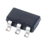
| 产品图片 |
|
| rohs | 符合RoHS无铅 / 符合限制有害物质指令(RoHS)规范要求 |
| 产品系列 | 逻辑集成电路,变换器,Texas Instruments SN74LVC2G14DBVT74LVC |
| 数据手册 | |
| 产品型号 | SN74LVC2G14DBVT |
| PCN组件/产地 | |
| 不同V、最大CL时的最大传播延迟 | 4.3ns @ 5V,50pF |
| 产品种类 | 变换器 |
| 低电平输出电流 | 32 mA |
| 供应商器件封装 | SOT-23-6 |
| 其它名称 | 296-26618-2 |
| 包装 | 带卷 (TR) |
| 单位重量 | 15.800 mg |
| 商标 | Texas Instruments |
| 安装类型 | 表面贴装 |
| 安装风格 | SMD/SMT |
| 封装 | Reel |
| 封装/外壳 | SOT-23-6 |
| 封装/箱体 | SOT-23-6 |
| 工作温度 | -40°C ~ 125°C |
| 工厂包装数量 | 250 |
| 最大工作温度 | + 85 C |
| 标准包装 | 250 |
| 特性 | 施密特触发器 |
| 电压-电源 | 1.65 V ~ 5.5 V |
| 电流-输出高,低 | 32mA,32mA |
| 电流-静态(最大值) | 10µA |
| 电源电压-最大 | 5.5 V |
| 电源电压-最小 | 1.65 V |
| 电路数 | 2 |
| 电路数量 | 2 Circuit |
| 系列 | SN74LVC2G14 |
| 输入数 | 2 |
| 逻辑电平-低 | 0.3 V ~ 1.4 V |
| 逻辑电平-高 | 1.4 V ~ 3.7 V |
| 逻辑类型 | |
| 逻辑系列 | LVC |
| 高电平输出电流 | - 32 mA |


- 商务部:美国ITC正式对集成电路等产品启动337调查
- 曝三星4nm工艺存在良率问题 高通将骁龙8 Gen1或转产台积电
- 太阳诱电将投资9.5亿元在常州建新厂生产MLCC 预计2023年完工
- 英特尔发布欧洲新工厂建设计划 深化IDM 2.0 战略
- 台积电先进制程称霸业界 有大客户加持明年业绩稳了
- 达到5530亿美元!SIA预计今年全球半导体销售额将创下新高
- 英特尔拟将自动驾驶子公司Mobileye上市 估值或超500亿美元
- 三星加码芯片和SET,合并消费电子和移动部门,撤换高东真等 CEO
- 三星电子宣布重大人事变动 还合并消费电子和移动部门
- 海关总署:前11个月进口集成电路产品价值2.52万亿元 增长14.8%


PDF Datasheet 数据手册内容提取
Product Sample & Technical Tools & Support & Reference Folder Buy Documents Software Community Design SN74LVC2G14 SCES200O–APRIL1999–REVISEDAUGUST2015 SN74LVC2G14 Dual Schmitt-Trigger Inverter 1 Features 3 Description • AvailableintheTINanoFree™Package This dual Schmitt-trigger inverter is designed for 1 1.65-Vto5.5-VV operation. • Supports5-VV Operation CC CC NanoFree™ package technology is a major • InputsAcceptVoltagesto5.5V breakthrough in IC packaging concepts, using the die • Maxt of5.4nsat3.3V pd asthepackage. • Low-PowerConsumption,10-μAMaximumI CC The SN74LVC2G14 device contains two inverters • ±24-mAOutputDriveat3.3V and performs the Boolean function Y = A. The device • TypicalV (OutputGroundBounce) functions as two independent inverters, but because OLP <0.8VatV =3.3V,T =25°C ofSchmittaction,itmayhavedifferentinputthreshold CC A levels for positive-going (V ) and negative-going • TypicalV (OutputV Undershoot) T+ OHV OH (V )signals. >2VatV =3.3V,T =25°C T– CC A • I SupportsLiveInsertion,Partial-Power-Down This device is fully specified for partial-power-down off Mode,andBack-DriveProtection applications using Ioff. The Ioff circuitry disables the outputs, preventing damaging current backflow • SupportTranslationDown throughthedevicewhenitispowereddown. (5Vto3.3V;3.3Vto1.8V) • Latch-UpPerformanceExceeds100mA DeviceInformation(1) PerJESD78,ClassII PARTNUMBER PACKAGE BODYSIZE(NOM) SN74LVC2G14DBV SOT-23(6) 2.90mm×1.60mm 2 Applications SN74LVC2G14DCK SC70(6) 2.00mm×1.25mm • BodyControlModules SN74LVC2G14YZP DSBGA(6) 1.41mm×0.91mm • EngineControlModules (1) For all available packages, see the orderable addendum at theendofthedatasheet. • Arcade,Casino,andGamblingMachines • ServersandHigh-PerformanceComputing • EPOS,ECR,andCashDrawer • Routers • DesktopPC BlockDiagram 1 6 1A 1Y 3 4 2A 2Y 1 An IMPORTANT NOTICE at the end of this data sheet addresses availability, warranty, changes, use in safety-critical applications, intellectualpropertymattersandotherimportantdisclaimers.PRODUCTIONDATA.
SN74LVC2G14 SCES200O–APRIL1999–REVISEDAUGUST2015 www.ti.com Table of Contents 1 Features.................................................................. 1 8.1 Overview...................................................................8 2 Applications........................................................... 1 8.2 FunctionalBlockDiagram.........................................8 3 Description............................................................. 1 8.3 FeatureDescription...................................................8 8.4 DeviceFunctionalModes..........................................8 4 RevisionHistory..................................................... 2 9 ApplicationandImplementation.......................... 9 5 PinConfigurationandFunctions......................... 3 9.1 ApplicationInformation..............................................9 6 Specifications......................................................... 4 9.2 TypicalApplication ...................................................9 6.1 AbsoluteMaximumRatings .....................................4 10 PowerSupplyRecommendations..................... 10 6.2 ESDRatings ............................................................4 11 Layout................................................................... 10 6.3 RecommendedOperatingConditions......................4 6.4 ThermalInformation..................................................5 11.1 LayoutGuidelines.................................................10 6.5 ElectricalCharacteristics...........................................5 11.2 LayoutExample....................................................11 6.6 SwitchingCharacteristics,–40°Cto85°C................6 12 DeviceandDocumentationSupport................. 12 6.7 SwitchingCharacteristics,–40°Cto125°C...............6 12.1 CommunityResources..........................................12 6.8 OperatingCharacteristics..........................................6 12.2 Trademarks...........................................................12 6.9 TypicalCharacteristics..............................................6 12.3 ElectrostaticDischargeCaution............................12 7 ParameterMeasurementInformation..................7 12.4 Glossary................................................................12 8 DetailedDescription.............................................. 8 13 Mechanical,Packaging,andOrderable Information........................................................... 12 4 Revision History NOTE:Pagenumbersforpreviousrevisionsmaydifferfrompagenumbersinthecurrentversion. ChangesfromRevisionN(June2015)toRevisionO Page • AddedT junctiontemperaturespectoAbsMaxRatings...................................................................................................... 4 J ChangesfromRevisionM(November2013)toRevisionN Page • AddedApplications,DeviceInformationtable,ESDRatingstable,FeatureDescriptionsection,DeviceFunctional Modes,ApplicationandImplementationsection,PowerSupplyRecommendationssection,Layoutsection,Device andDocumentationSupportsection,andMechanical,Packaging,andOrderableInformationsection .............................. 1 2 SubmitDocumentationFeedback Copyright©1999–2015,TexasInstrumentsIncorporated ProductFolderLinks:SN74LVC2G14
SN74LVC2G14 www.ti.com SCES200O–APRIL1999–REVISEDAUGUST2015 5 Pin Configuration and Functions DBVPackage 6-PinSOT-23 DCKPackage TopView 6-PinSC70 TopView 1A 1 6 1Y 1A 1 6 1Y GND 2 5 VCC GND 2 5 VCC 2A 3 4 2Y 2A 3 4 2Y YZPPackage 6-PinDSBGA BottomView 2A 34 2Y GND 25 VCC 1A 16 1Y Seemechanicaldrawingfordimensions. PinFunctions PIN I/O DESCRIPTION NAME NO. 1A 1 I Gate1logicsignal 1Y 6 O Gate1invertedsignal 2A 3 I Gate2logicsignal 2Y 4 O Gate2invertedsignal GND 2 — Ground V 5 — Supply/PowerPin CC Copyright©1999–2015,TexasInstrumentsIncorporated SubmitDocumentationFeedback 3 ProductFolderLinks:SN74LVC2G14
SN74LVC2G14 SCES200O–APRIL1999–REVISEDAUGUST2015 www.ti.com 6 Specifications 6.1 Absolute Maximum Ratings overoperatingfree-airtemperaturerange(unlessotherwisenoted)(1) MIN MAX UNIT V Supplyvoltage –0.5 6.5 V CC V Inputvoltage(2) –0.5 6.5 V I V Voltageappliedtoanyoutputinthehigh-impedanceorpower-offstate(2) –0.5 6.5 V O V Voltageappliedtoanyoutputinthehighorlowstate(2)(3) –0.5 V +0.5 V O CC I Inputclampcurrent V <0 –50 mA IK I I Outputclampcurrent V <0 –50 mA OK O I Continuousoutputcurrent ±50 mA O ContinuouscurrentthroughV orGND ±100 mA CC T Junctiontemperature –65 150 °C J T Storagetemperature –65 150 °C stg (1) StressesbeyondthoselistedunderAbsoluteMaximumRatingsmaycausepermanentdamagetothedevice.Thesearestressratings only,whichdonotimplyfunctionaloperationofthedeviceattheseoranyotherconditionsbeyondthoseindicatedunderRecommended OperatingConditions.Exposuretoabsolute-maximum-ratedconditionsforextendedperiodsmayaffectdevicereliability. (2) Theinputnegative-voltageandoutputvoltageratingsmaybeexceedediftheinputandoutputclamp-currentratingsareobserved. (3) ThevalueofV isprovidedintheRecommendedOperatingConditionstable. CC 6.2 ESD Ratings VALUE UNIT Human-bodymodel(HBM),perANSI/ESDA/JEDECJS-001(1) ±2000 V(ESD) Electrostaticdischarge Charged-devicemodel(CDM),perJEDECspecificationJESD22- V C101(2) ±1000 (1) JEDECdocumentJEP155statesthat500-VHBMallowssafemanufacturingwithastandardESDcontrolprocess.Manufacturingwith lessthan500-VHBMispossiblewiththenecessaryprecautions.Pinslistedas±XXXVmayactuallyhavehigherperformance. (2) JEDECdocumentJEP157statesthat250-VCDMallowssafemanufacturingwithastandardESDcontrolprocess.Manufacturingwith lessthan250-VCDMispossiblewiththenecessaryprecautions.Pinslistedas±YYYVmayactuallyhavehigherperformance. 6.3 Recommended Operating Conditions See (1) MIN MAX UNIT Operating 1.65 5.5 V Supplyvoltage V CC Dataretentiononly 1.5 V Inputvoltage 0 5.5 V I V Outputvoltage 0 V V O CC V =1.65V –4 CC V =2.3V –8 CC I High-leveloutputcurrent –16 mA OH V =3V CC –24 V =4.5V –32 CC V =1.65V 4 CC V =2.3V 8 CC I Low-leveloutputcurrent 16 mA OL V =3V CC 24 V =4.5V 32 CC T Operatingfree-airtemperature –40 125 °C A (1) AllunusedinputsofthedevicemustbeheldatV orGNDtoensureproperdeviceoperation.RefertotheTIapplicationreport, CC ImplicationsofSloworFloatingCMOSInputs,SCBA004. 4 SubmitDocumentationFeedback Copyright©1999–2015,TexasInstrumentsIncorporated ProductFolderLinks:SN74LVC2G14
SN74LVC2G14 www.ti.com SCES200O–APRIL1999–REVISEDAUGUST2015 6.4 Thermal Information SN74LVC2G14 THERMALMETRIC(1) DBV(SOT23) DCK(SC70) YZP(DSBGA) UNIT 6PINS 6PINS 6PINS R Junction-to-ambientthermalresistance 215 259 139 °C/W θJA R Junction-to-case(top)thermalresistance 55 87 18 °C/W θJC(top) R Junction-to-boardthermalresistance 57 89 N/A °C/W θJB (1) Formoreinformationabouttraditionalandnewthermalmetrics,seetheSemiconductorandICPackageThermalMetricsapplication report,SPRA953. 6.5 Electrical Characteristics overrecommendedoperatingfree-airtemperaturerange(unlessotherwisenoted) –40°Cto85°C –40°Cto125°C PARAMETER TESTCONDITIONS VCC MIN TYP(1) MAX MIN TYP(1) MAX UNIT 1.65V 0.7 1.4 0.7 1.4 2.3V 1 1.7 1 1.7 VT+ Positive-goinginput 3V 1.3 2.2 1.3 2.2 V thresholdvoltage 4.5V 1.9 3.1 1.9 3.1 5.5V 2.2 3.7 2.2 3.7 1.65V 0.3 0.7 0.3 0.7 2.3V 0.4 1 0.4 1 VT– Negative-goinginput 3V 0.6 1.3 0.6 1.3 V thresholdvoltage 4.5V 1.1 2 1.1 2 5.5V 1.4 2.5 1.4 2.5 1.65V 0.3 0.8 0.3 0.8 2.3V 0.4 0.9 0.4 0.9 ΔVT Hysteresis 3V 0.4 1.1 0.4 1.1 V (VT+–VT–) 4.5V 0.6 1.3 0.6 1.3 5.5V 0.7 1.4 0.7 1.4 IOH=–100μA 1.65Vto4.5V VCC–0.1 VCC–0.1 IOH=–4mA 1.65V 1.2 1.2 IOH=–8mA 2.3V 1.9 1.9 VOH V IOH=–16mA 3V 2.4 2.4 IOH=–24mA 3V 2.3 2.3 IOH=–32mA 4.5V 3.8 3.8 IOL=100μA 1.65Vto4.5V 0.1 0.1 IOL=4mA 1.65V 0.45 0.45 IOL=8mA 2.3V 0.3 0.3 VOL V IOL=16mA 3V 0.4 0.4 IOL=24mA 3V 0.55 0.55 IOL=32mA 4.5V 0.55 0.55 II Ainput VI=5.5VorGND 0to5.5V ±5 ±5 μA Ioff VIorVO=5.5V 0 ±10 ±10 μA ICC VI=5.5VorGND, IO=0 1.65Vto5.5V 10 10 μA ΔICC OOntheerinipnuptuatstaVtCVCC–C0o.r6GVN,D 3Vto5.5V 500 500 μA CI VI=VCCorGND 3.3V 4 pF (1) AlltypicalvaluesareatV =3.3V,T =25°C. CC A Copyright©1999–2015,TexasInstrumentsIncorporated SubmitDocumentationFeedback 5 ProductFolderLinks:SN74LVC2G14
SN74LVC2G14 SCES200O–APRIL1999–REVISEDAUGUST2015 www.ti.com 6.6 Switching Characteristics, –40°C to 85°C overrecommendedoperatingfree-airtemperaturerange(unlessotherwisenoted)(seeFigure3) VCC=1.8V VCC=2.5V VCC=3.3V VCC=5V PARAMETER FROM TO ±0.15V ±0.2V ±0.3V ±0.5V UNIT (INPUT) (OUTPUT) MIN MAX MIN MAX MIN MAX MIN MAX tpd A Y 3.9 9.5 1.9 5.7 2 5.4 1.5 4.3 ns 6.7 Switching Characteristics, –40°C to 125°C overrecommendedoperatingfree-airtemperaturerange(unlessotherwisenoted)(seeFigure3) VCC=1.8V VCC=2.5V VCC=3.3V VCC=5V PARAMETER FROM TO ±0.15V ±0.2V ±0.3V ±0.5V UNIT (INPUT) (OUTPUT) MIN MAX MIN MAX MIN MAX MIN MAX tpd A Y 3.9 10.5 1.9 6.5 2 6 1.5 4.7 ns 6.8 Operating Characteristics T =25°C A V =1.8V V =2.5V V =3.3V V =5V CC CC CC CC PARAMETER TESTCONDITIONS UNIT TYP TYP TYP TYP C Powerdissipationcapacitance f=10MHz 16 17 18 21 pF pd 6.9 Typical Characteristics 8 TPD 7 6 5 s) ns) (n D ( 4 D TP P 3 T 2 1 0 0 1 2 3 4 5 6 VCC (V) D002 Temperature (°C) Figure1.TPDAcrossTemperatureat3.3VVCC Figure2.TPDAcrossVCCat25°C 6 SubmitDocumentationFeedback Copyright©1999–2015,TexasInstrumentsIncorporated ProductFolderLinks:SN74LVC2G14
SN74LVC2G14 www.ti.com SCES200O–APRIL1999–REVISEDAUGUST2015 7 Parameter Measurement Information V LOAD R S1 Open From Output L TEST S1 Under Test GND t /t Open C PLH PHL (see NoteA)L RL tPLZ/tPZL VLOAD t /t GND PHZ PZH LOAD CIRCUIT INPUTS V V V C R V CC V t/t M LOAD L L D I r f 1.8 V±0.15 V V £2 ns V /2 2 ×V 30 pF 1 kW 0.15 V CC CC CC 2.5 V±0.2 V V £2 ns V /2 2 ×V 30 pF 500W 0.15 V CC CC CC 3.3 V±0.3 V 3 V £2.5 ns 1.5 V 6 V 50 pF 500W 0.3 V 5 V±0.5 V V £2.5 ns V /2 2 ×V 50 pF 500W 0.3 V CC CC CC V I Timing Input V M 0 V t W VI tsu th V Input V V I M M Data Input V V M M 0 V 0 V VOLTAGE WAVEFORMS VOLTAGE WAVEFORMS PULSE DURATION SETUPAND HOLD TIMES Input VM VM VI COounttpruotl VM VM VI 0 V 0 V t t t t PLH PHL PZL PLZ V Output V /2 Output VM VM OH WSav1e afot rVm 1 VM V + V LOAD VOL (see NoteL OBAD) OL D VOL t t PHL PLH t t PZH PHZ Output VM VM VOH WSa1v eaOfto uGrtmpNu D2t VM VOH–VD VOH VOL (see Note B) »0 V VOLTAGE WAVEFORMS VOLTAGE WAVEFORMS PROPAGATION DELAYTIMES ENABLEAND DISABLE TIMES INVERTINGAND NONINVERTING OUTPUTS LOW-AND HIGH-LEVELENABLING NOTES: A. C includes probe and jig capacitance. L B. Waveform 1 is for an output with internal conditions such that the output is low, except when disabled by the output control. Waveform 2 is for an output with internal conditions such that the output is high, except when disabled by the output control. C. All input pulses are supplied by generators having the following characteristics: PRR£10 MHz, Z = 50W. O D. The outputs are measured one at a time, with one transition per measurement. E. t and t are the same as t . PLZ PHZ dis F. t and t are the same as t . PZL PZH en G.t and t are the same as t . PLH PHL pd H. All parameters and waveforms are not applicable to all devices. Figure3. LoadCircuitandVoltageWaveforms Copyright©1999–2015,TexasInstrumentsIncorporated SubmitDocumentationFeedback 7 ProductFolderLinks:SN74LVC2G14
SN74LVC2G14 SCES200O–APRIL1999–REVISEDAUGUST2015 www.ti.com 8 Detailed Description 8.1 Overview The SN74LVC2G14 device contains two Schmitt Trigger Inverter and performs the Boolean function Y = A. The device functions as an independent inverter, but because of Schmitt Trigger action, it will have different input thresholdlevelsforapositive-going(V )andnegative-going(V )signals. t+ t- This device is fully specified for partial-power-down applications using I . The I circuit disables the output, off off preventingdamagingcurrentback-flowthroughthedevicewhenitispowereddown. 8.2 Functional Block Diagram 1 6 1A 1Y 3 4 2A 2Y 8.3 Feature Description 8.3.1 SupportTranslationDown(5Vto3.3V;3.3Vto1.8V) As the inputs are 5.5-V tolerant, the device can be used as a down translator. When the input voltage exceeds V ,theoutputwillfollowV ,performingdown-translationiftheinputvoltageexceedsV . T+(Max) CC CC 8.4 Device Functional Modes Table1liststhefunctionalmodesoftheSN74LVC2G14. Table1.FunctionalTable (EachInverter) INPUT OUTPUT A Y H L L H 8 SubmitDocumentationFeedback Copyright©1999–2015,TexasInstrumentsIncorporated ProductFolderLinks:SN74LVC2G14
SN74LVC2G14 www.ti.com SCES200O–APRIL1999–REVISEDAUGUST2015 9 Application and Implementation NOTE Information in the following applications sections is not part of the TI component specification, and TI does not warrant its accuracy or completeness. TI’s customers are responsible for determining suitability of components for their purposes. Customers should validateandtesttheirdesignimplementationtoconfirmsystemfunctionality. 9.1 Application Information The SN74LVC2G14 device is a high-drive CMOS device that can be used for a multitude of buffer type functions where the input is slow or noisy. The device can produce 24 mA of drive current at 3.3 V, making it Ideal for driving multiple outputs and good for high-speed applications up to 100 MHz. The inputs are 5.5-V tolerant allowingittotranslatedowntoV . CC 9.2 Typical Application ~2.2M(cid:13)(cid:3) SN74LVC2G14 (one channel) 50 pF 16 pF ~32 pF ~32pF Figure4. TypicalApplicationSchematic 9.2.1 DesignRequirements This device uses CMOS technology and has balanced output drive. Care should be taken to avoid bus contention because it can drive currents that would exceed maximum limits. The high drive will also create fast edgesintolightloadssoroutingandloadconditionsshouldbeconsideredtopreventringing. 9.2.2 DetailedDesignProcedure 1. RecommendedInputConditions – Risetimeandfalltimespecs.See(Δt/ΔV)intheRecommendedOperatingConditionstable. – Specifiedhighandlowlevels.See(V andV )intheRecommendedOperatingConditions table. IH IL – Inputs are overvoltage tolerant allowing them to go as high as (V max) in the Recommended Operating I ConditionstableatanyvalidV . CC 2. RecommendOutputConditions – Load currents should not exceed (I max) per output and should not exceed (continuous current through O V orGND)totalcurrentforthepart.TheselimitsarelocatedintheAbsoluteMaximumRatings table. CC – OutputsshouldnotbepulledaboveV . CC Copyright©1999–2015,TexasInstrumentsIncorporated SubmitDocumentationFeedback 9 ProductFolderLinks:SN74LVC2G14
SN74LVC2G14 SCES200O–APRIL1999–REVISEDAUGUST2015 www.ti.com Typical Application (continued) 9.2.3 ApplicationCurve 10 Icc 1.8V 9 Icc 2.5V 8 Icc 3.3V Icc 5V 7 6 A m c - 5 Ic 4 3 2 1 0 0 20 40 60 80 Frequency - MHz D003 Figure5.ICCvsFrequency 10 Power Supply Recommendations The power supply can be any voltage between the minimum and maximum supply voltage rating located in the table. Each V pin should have a good bypass capacitor to prevent power disturbance. For devices with a CC single supply, TI recommends a 0.1-μF capacitor. If there are multiple V pins, then TI recommends a 0.01-μF CC or 0.022-μF capacitor for each power pin. It is ok to parallel multiple bypass capacitors to reject different frequencies of noise. 0.1-μF and 1-μF capacitors are commonly used in parallel. The bypass capacitor should be installedasclosetothepowerpinaspossibleforbestresults. 11 Layout 11.1 Layout Guidelines When using multiple bit logic devices inputs should not ever float. In many cases, functions or parts of functions of digital logic devices are unused, for example, when only two inputs of a triple-input AND gate are used or only 3 of the 4 buffer gates are used. Such input terminals should not be left unconnected because the undefined voltages at the outside connections result in undefined operational states. The following rules must be observed underallcircumstances: • All unused inputs of digital logic devices must be connected to a high or low bias to prevent them from floating. • The logic level that should be applied to any particular unused input depends on the function of the device. GenerallytheywillbetiedtoGNDorV whichevermakemoresenseorismoreconvenient. CC 10 SubmitDocumentationFeedback Copyright©1999–2015,TexasInstrumentsIncorporated ProductFolderLinks:SN74LVC2G14
SN74LVC2G14 www.ti.com SCES200O–APRIL1999–REVISEDAUGUST2015 11.2 Layout Example V DD Keep signal traces as short as possible 0.1µF 1A 1 6 1Y GND 2 SN74LVC2G14 5 V CC 2A 3 4 2Y Unused inputs connected to GND or V to prevent CC floating Figure6. LayoutSchematic Copyright©1999–2015,TexasInstrumentsIncorporated SubmitDocumentationFeedback 11 ProductFolderLinks:SN74LVC2G14
SN74LVC2G14 SCES200O–APRIL1999–REVISEDAUGUST2015 www.ti.com 12 Device and Documentation Support 12.1 Community Resources The following links connect to TI community resources. Linked contents are provided "AS IS" by the respective contributors. They do not constitute TI specifications and do not necessarily reflect TI's views; see TI's Terms of Use. TIE2E™OnlineCommunity TI'sEngineer-to-Engineer(E2E)Community.Createdtofostercollaboration amongengineers.Ate2e.ti.com,youcanaskquestions,shareknowledge,exploreideasandhelp solveproblemswithfellowengineers. DesignSupport TI'sDesignSupport QuicklyfindhelpfulE2Eforumsalongwithdesignsupporttoolsand contactinformationfortechnicalsupport. 12.2 Trademarks NanoFree,E2EaretrademarksofTexasInstruments. Allothertrademarksarethepropertyoftheirrespectiveowners. 12.3 Electrostatic Discharge Caution Thesedeviceshavelimitedbuilt-inESDprotection.Theleadsshouldbeshortedtogetherorthedeviceplacedinconductivefoam duringstorageorhandlingtopreventelectrostaticdamagetotheMOSgates. 12.4 Glossary SLYZ022—TIGlossary. Thisglossarylistsandexplainsterms,acronyms,anddefinitions. 13 Mechanical, Packaging, and Orderable Information The following pages include mechanical packaging and orderable information. This information is the most current data available for the designated devices. This data is subject to change without notice and revision of thisdocument.Forbrowserbasedversionsofthisdatasheet,refertothelefthandnavigation. 12 SubmitDocumentationFeedback Copyright©1999–2015,TexasInstrumentsIncorporated ProductFolderLinks:SN74LVC2G14
PACKAGE OPTION ADDENDUM www.ti.com 6-Feb-2020 PACKAGING INFORMATION Orderable Device Status Package Type Package Pins Package Eco Plan Lead/Ball Finish MSL Peak Temp Op Temp (°C) Device Marking Samples (1) Drawing Qty (2) (6) (3) (4/5) SN74LVC2G14DBVR ACTIVE SOT-23 DBV 6 3000 Green (RoHS NIPDAU | SN Level-1-260C-UNLIM -40 to 125 (C145, C14F, C14K, & no Sb/Br) C14R) SN74LVC2G14DBVRE4 ACTIVE SOT-23 DBV 6 3000 Green (RoHS NIPDAU Level-1-260C-UNLIM -40 to 125 (C14F, C14R) & no Sb/Br) SN74LVC2G14DBVRG4 ACTIVE SOT-23 DBV 6 3000 Green (RoHS NIPDAU Level-1-260C-UNLIM -40 to 125 (C14F, C14R) & no Sb/Br) SN74LVC2G14DBVT ACTIVE SOT-23 DBV 6 250 Green (RoHS NIPDAU | SN Level-1-260C-UNLIM -40 to 125 (C145, C14F, C14K, & no Sb/Br) C14R) SN74LVC2G14DBVTG4 ACTIVE SOT-23 DBV 6 250 Green (RoHS NIPDAU Level-1-260C-UNLIM -40 to 125 (C14F, C14R) & no Sb/Br) SN74LVC2G14DCK3 ACTIVE SC70 DCK 6 3000 Pb-Free SNBI Level-1-260C-UNLIM -40 to 125 (CFF, CFZ) (RoHS) SN74LVC2G14DCKR ACTIVE SC70 DCK 6 3000 Green (RoHS NIPDAU | SN Level-1-260C-UNLIM -40 to 125 (CF5, CFF, CFJ, CF & no Sb/Br) K, CFR) SN74LVC2G14DCKRE4 ACTIVE SC70 DCK 6 3000 Green (RoHS NIPDAU Level-1-260C-UNLIM -40 to 125 CF5 & no Sb/Br) SN74LVC2G14DCKRG4 ACTIVE SC70 DCK 6 3000 Green (RoHS NIPDAU Level-1-260C-UNLIM -40 to 125 CF5 & no Sb/Br) SN74LVC2G14DCKT ACTIVE SC70 DCK 6 250 Green (RoHS NIPDAU | SN Level-1-260C-UNLIM -40 to 125 (CF5, CFF, CFJ, CF & no Sb/Br) K, CFR) SN74LVC2G14DCKTG4 ACTIVE SC70 DCK 6 250 Green (RoHS NIPDAU Level-1-260C-UNLIM -40 to 125 CF5 & no Sb/Br) SN74LVC2G14YZPR ACTIVE DSBGA YZP 6 3000 Green (RoHS SNAGCU Level-1-260C-UNLIM -40 to 125 (CF7, CFN) & no Sb/Br) (1) The marketing status values are defined as follows: ACTIVE: Product device recommended for new designs. LIFEBUY: TI has announced that the device will be discontinued, and a lifetime-buy period is in effect. NRND: Not recommended for new designs. Device is in production to support existing customers, but TI does not recommend using this part in a new design. PREVIEW: Device has been announced but is not in production. Samples may or may not be available. OBSOLETE: TI has discontinued the production of the device. (2) RoHS: TI defines "RoHS" to mean semiconductor products that are compliant with the current EU RoHS requirements for all 10 RoHS substances, including the requirement that RoHS substance do not exceed 0.1% by weight in homogeneous materials. Where designed to be soldered at high temperatures, "RoHS" products are suitable for use in specified lead-free processes. TI may reference these types of products as "Pb-Free". RoHS Exempt: TI defines "RoHS Exempt" to mean products that contain lead but are compliant with EU RoHS pursuant to a specific EU RoHS exemption. Addendum-Page 1
PACKAGE OPTION ADDENDUM www.ti.com 6-Feb-2020 Green: TI defines "Green" to mean the content of Chlorine (Cl) and Bromine (Br) based flame retardants meet JS709B low halogen requirements of <=1000ppm threshold. Antimony trioxide based flame retardants must also meet the <=1000ppm threshold requirement. (3) MSL, Peak Temp. - The Moisture Sensitivity Level rating according to the JEDEC industry standard classifications, and peak solder temperature. (4) There may be additional marking, which relates to the logo, the lot trace code information, or the environmental category on the device. (5) Multiple Device Markings will be inside parentheses. Only one Device Marking contained in parentheses and separated by a "~" will appear on a device. If a line is indented then it is a continuation of the previous line and the two combined represent the entire Device Marking for that device. (6) Lead/Ball Finish - Orderable Devices may have multiple material finish options. Finish options are separated by a vertical ruled line. Lead/Ball Finish values may wrap to two lines if the finish value exceeds the maximum column width. Important Information and Disclaimer:The information provided on this page represents TI's knowledge and belief as of the date that it is provided. TI bases its knowledge and belief on information provided by third parties, and makes no representation or warranty as to the accuracy of such information. Efforts are underway to better integrate information from third parties. TI has taken and continues to take reasonable steps to provide representative and accurate information but may not have conducted destructive testing or chemical analysis on incoming materials and chemicals. TI and TI suppliers consider certain information to be proprietary, and thus CAS numbers and other limited information may not be available for release. In no event shall TI's liability arising out of such information exceed the total purchase price of the TI part(s) at issue in this document sold by TI to Customer on an annual basis. OTHER QUALIFIED VERSIONS OF SN74LVC2G14 : •Automotive: SN74LVC2G14-Q1 NOTE: Qualified Version Definitions: •Automotive - Q100 devices qualified for high-reliability automotive applications targeting zero defects Addendum-Page 2
PACKAGE MATERIALS INFORMATION www.ti.com 2-Feb-2020 TAPE AND REEL INFORMATION *Alldimensionsarenominal Device Package Package Pins SPQ Reel Reel A0 B0 K0 P1 W Pin1 Type Drawing Diameter Width (mm) (mm) (mm) (mm) (mm) Quadrant (mm) W1(mm) SN74LVC2G14DBVR SOT-23 DBV 6 3000 178.0 9.2 3.3 3.23 1.55 4.0 8.0 Q3 SN74LVC2G14DBVR SOT-23 DBV 6 3000 180.0 8.4 3.23 3.17 1.37 4.0 8.0 Q3 SN74LVC2G14DBVRG4 SOT-23 DBV 6 3000 178.0 9.0 3.23 3.17 1.37 4.0 8.0 Q3 SN74LVC2G14DBVT SOT-23 DBV 6 250 178.0 9.2 3.3 3.23 1.55 4.0 8.0 Q3 SN74LVC2G14DBVT SOT-23 DBV 6 250 180.0 8.4 3.23 3.17 1.37 4.0 8.0 Q3 SN74LVC2G14DBVTG4 SOT-23 DBV 6 250 178.0 9.0 3.23 3.17 1.37 4.0 8.0 Q3 SN74LVC2G14DCKR SC70 DCK 6 3000 180.0 8.4 2.41 2.41 1.2 4.0 8.0 Q3 SN74LVC2G14DCKR SC70 DCK 6 3000 178.0 9.2 2.4 2.4 1.22 4.0 8.0 Q3 SN74LVC2G14DCKR SC70 DCK 6 3000 178.0 9.0 2.4 2.5 1.2 4.0 8.0 Q3 SN74LVC2G14DCKRG4 SC70 DCK 6 3000 178.0 9.2 2.4 2.4 1.22 4.0 8.0 Q3 SN74LVC2G14DCKT SC70 DCK 6 250 178.0 9.0 2.4 2.5 1.2 4.0 8.0 Q3 SN74LVC2G14DCKT SC70 DCK 6 250 180.0 8.4 2.41 2.41 1.2 4.0 8.0 Q3 SN74LVC2G14DCKTG4 SC70 DCK 6 250 178.0 9.2 2.4 2.4 1.22 4.0 8.0 Q3 SN74LVC2G14YZPR DSBGA YZP 6 3000 178.0 9.2 1.02 1.52 0.63 4.0 8.0 Q1 PackMaterials-Page1
PACKAGE MATERIALS INFORMATION www.ti.com 2-Feb-2020 *Alldimensionsarenominal Device PackageType PackageDrawing Pins SPQ Length(mm) Width(mm) Height(mm) SN74LVC2G14DBVR SOT-23 DBV 6 3000 180.0 180.0 18.0 SN74LVC2G14DBVR SOT-23 DBV 6 3000 202.0 201.0 28.0 SN74LVC2G14DBVRG4 SOT-23 DBV 6 3000 180.0 180.0 18.0 SN74LVC2G14DBVT SOT-23 DBV 6 250 180.0 180.0 18.0 SN74LVC2G14DBVT SOT-23 DBV 6 250 202.0 201.0 28.0 SN74LVC2G14DBVTG4 SOT-23 DBV 6 250 180.0 180.0 18.0 SN74LVC2G14DCKR SC70 DCK 6 3000 202.0 201.0 28.0 SN74LVC2G14DCKR SC70 DCK 6 3000 180.0 180.0 18.0 SN74LVC2G14DCKR SC70 DCK 6 3000 180.0 180.0 18.0 SN74LVC2G14DCKRG4 SC70 DCK 6 3000 180.0 180.0 18.0 SN74LVC2G14DCKT SC70 DCK 6 250 180.0 180.0 18.0 SN74LVC2G14DCKT SC70 DCK 6 250 202.0 201.0 28.0 SN74LVC2G14DCKTG4 SC70 DCK 6 250 180.0 180.0 18.0 SN74LVC2G14YZPR DSBGA YZP 6 3000 220.0 220.0 35.0 PackMaterials-Page2
PACKAGE OUTLINE DBV0006A SOT-23 - 1.45 mm max height SCALE 4.000 SMALL OUTLINE TRANSISTOR C 3.0 2.6 0.1 C 1.75 1.45 B A 1.45 MAX PIN 1 INDEX AREA 1 6 2X 0.95 3.05 2.75 1.9 5 2 4 3 0.50 6X 0.25 0.15 0.2 C A B (1.1) TYP 0.00 0.25 GAGE PLANE 0.22 TYP 0.08 8 TYP 0.6 0 0.3 TYP SEATING PLANE 4214840/B 03/2018 NOTES: 1. All linear dimensions are in millimeters. Any dimensions in parenthesis are for reference only. Dimensioning and tolerancing per ASME Y14.5M. 2. This drawing is subject to change without notice. 3. Body dimensions do not include mold flash or protrusion. Mold flash and protrusion shall not exceed 0.15 per side. 4. Leads 1,2,3 may be wider than leads 4,5,6 for package orientation. 5. Refernce JEDEC MO-178. www.ti.com
EXAMPLE BOARD LAYOUT DBV0006A SOT-23 - 1.45 mm max height SMALL OUTLINE TRANSISTOR PKG 6X (1.1) 1 6X (0.6) 6 SYMM 2 5 2X (0.95) 3 4 (R0.05) TYP (2.6) LAND PATTERN EXAMPLE EXPOSED METAL SHOWN SCALE:15X SOLDER MASK SOLDER MASK METAL UNDER METAL OPENING OPENING SOLDER MASK EXPOSED METAL EXPOSED METAL 0.07 MAX 0.07 MIN ARROUND ARROUND NON SOLDER MASK SOLDER MASK DEFINED DEFINED (PREFERRED) SOLDER MASK DETAILS 4214840/B 03/2018 NOTES: (continued) 6. Publication IPC-7351 may have alternate designs. 7. Solder mask tolerances between and around signal pads can vary based on board fabrication site. www.ti.com
EXAMPLE STENCIL DESIGN DBV0006A SOT-23 - 1.45 mm max height SMALL OUTLINE TRANSISTOR PKG 6X (1.1) 1 6X (0.6) 6 SYMM 2 5 2X(0.95) 3 4 (R0.05) TYP (2.6) SOLDER PASTE EXAMPLE BASED ON 0.125 mm THICK STENCIL SCALE:15X 4214840/B 03/2018 NOTES: (continued) 8. Laser cutting apertures with trapezoidal walls and rounded corners may offer better paste release. IPC-7525 may have alternate design recommendations. 9. Board assembly site may have different recommendations for stencil design. www.ti.com
None
None
PACKAGE OUTLINE YZP0006 DSBGA - 0.5 mm max height SCALE 9.000 DIE SIZE BALL GRID ARRAY B E A BALL A1 CORNER D 0.5 MAX C SEATING PLANE 0.19 BALL TYP 0.05 C 0.15 0.5 TYP C SYMM 1 D: Max = 1.418 mm, Min =1 .358 mm B TYP 0.5 E: Max = 0.918 mm, Min =0 .858 mm TYP A 0.25 1 2 6X 0.21 SYMM 0.015 C A B 4219524/A 06/2014 NOTES: NanoFree Is a trademark of Texas Instruments. 1. All linear dimensions are in millimeters. Any dimensions in parenthesis are for reference only. Dimensioning and tolerancing per ASME Y14.5M. 2. This drawing is subject to change without notice. 3. NanoFreeTM package configuration. www.ti.com
EXAMPLE BOARD LAYOUT YZP0006 DSBGA - 0.5 mm max height DIE SIZE BALL GRID ARRAY (0.5) TYP 6X ( 0.225) 1 2 A (0.5) TYP B SYMM C SYMM LAND PATTERN EXAMPLE SCALE:40X ( 0.225) 0.05 MAX 0.05 MIN METAL METAL UNDER MASK SOLDER MASK ( 0.225) OPENING SOLDER MASK OPENING NON-SOLDER MASK DEFINED SOLDER MASK (PREFERRED) DEFINED SOLDER MASK DETAILS NOT TO SCALE 4219524/A 06/2014 NOTES: (continued) 4. Final dimensions may vary due to manufacturing tolerance considerations and also routing constraints. For more information, see Texas Instruments literature number SBVA017 (www.ti.com/lit/sbva017). www.ti.com
EXAMPLE STENCIL DESIGN YZP0006 DSBGA - 0.5 mm max height DIE SIZE BALL GRID ARRAY (0.5) TYP 6X ( 0.25) (R0.05) TYP 1 2 A (0.5) TYP B SYMM METAL TYP C SYMM SOLDER PASTE EXAMPLE BASED ON 0.1 mm THICK STENCIL SCALE:40X 4219524/A 06/2014 NOTES: (continued) 5. Laser cutting apertures with trapezoidal walls and rounded corners may offer better paste release. www.ti.com
IMPORTANTNOTICEANDDISCLAIMER TI PROVIDES TECHNICAL AND RELIABILITY DATA (INCLUDING DATASHEETS), DESIGN RESOURCES (INCLUDING REFERENCE DESIGNS), APPLICATION OR OTHER DESIGN ADVICE, WEB TOOLS, SAFETY INFORMATION, AND OTHER RESOURCES “AS IS” AND WITH ALL FAULTS, AND DISCLAIMS ALL WARRANTIES, EXPRESS AND IMPLIED, INCLUDING WITHOUT LIMITATION ANY IMPLIED WARRANTIES OF MERCHANTABILITY, FITNESS FOR A PARTICULAR PURPOSE OR NON-INFRINGEMENT OF THIRD PARTY INTELLECTUAL PROPERTY RIGHTS. These resources are intended for skilled developers designing with TI products. You are solely responsible for (1) selecting the appropriate TI products for your application, (2) designing, validating and testing your application, and (3) ensuring your application meets applicable standards, and any other safety, security, or other requirements. These resources are subject to change without notice. TI grants you permission to use these resources only for development of an application that uses the TI products described in the resource. Other reproduction and display of these resources is prohibited. No license is granted to any other TI intellectual property right or to any third party intellectual property right. TI disclaims responsibility for, and you will fully indemnify TI and its representatives against, any claims, damages, costs, losses, and liabilities arising out of your use of these resources. TI’s products are provided subject to TI’s Terms of Sale (www.ti.com/legal/termsofsale.html) or other applicable terms available either on ti.com or provided in conjunction with such TI products. TI’s provision of these resources does not expand or otherwise alter TI’s applicable warranties or warranty disclaimers for TI products. Mailing Address: Texas Instruments, Post Office Box 655303, Dallas, Texas 75265 Copyright © 2020, Texas Instruments Incorporated