ICGOO在线商城 > 集成电路(IC) > 逻辑 - 缓冲器,驱动器,接收器,收发器 > SN74LVC1G126DBVT
 Datasheet下载
- 型号: SN74LVC1G126DBVT
- 制造商: Texas Instruments
- 库位|库存: xxxx|xxxx
- 要求:
| 数量阶梯 | 香港交货 | 国内含税 |
| +xxxx | $xxxx | ¥xxxx |
查看当月历史价格
查看今年历史价格
SN74LVC1G126DBVT产品简介:
ICGOO电子元器件商城为您提供SN74LVC1G126DBVT由Texas Instruments设计生产,在icgoo商城现货销售,并且可以通过原厂、代理商等渠道进行代购。 SN74LVC1G126DBVT价格参考。Texas InstrumentsSN74LVC1G126DBVT封装/规格:逻辑 - 缓冲器,驱动器,接收器,收发器, Buffer, Non-Inverting 1 Element 1 Bit per Element 3-State Output SOT-23-5。您可以下载SN74LVC1G126DBVT参考资料、Datasheet数据手册功能说明书,资料中有SN74LVC1G126DBVT 详细功能的应用电路图电压和使用方法及教程。
SN74LVC1G126DBVT是Texas Instruments推出的一款单路非反相缓冲器/驱动器,属于逻辑缓冲器、驱动器、接收器及收发器类别。该器件工作电压范围为1.65V至5.5V,支持低电压操作,兼容多种逻辑电平,适用于现代低功耗数字系统。

其主要应用场景包括:在便携式电子产品(如智能手机、平板电脑、可穿戴设备)中用于信号电平转换和驱动能力增强;在通信接口电路中作为线路驱动器,提升信号完整性;在微控制器与外围设备之间实现信号隔离与缓冲,防止负载过重影响主控性能;还可用于LED驱动、开关控制及数字信号调理等场合。

该芯片采用SOT-23-5小型封装,节省PCB空间,适合高密度布局设计。内置三态输出功能,支持总线应用中的多设备共享线路,提高系统灵活性。凭借其高噪声抑制能力和快速开关特性,SN74LVC1G126DBVT广泛应用于消费电子、工业控制、通信模块和嵌入式系统等领域,是一款高性能、低功耗的单通道缓冲驱动解决方案。
| 参数 | 数值 |
| 产品目录 | 集成电路 (IC)半导体 |
| 描述 | IC BUS BUFF TRI-ST N-INV SOT23-5缓冲器和线路驱动器 SNGL Bus Buffer Gate |
| 产品分类 | |
| 品牌 | Texas Instruments |
| 产品手册 | http://www.ti.com/lit/gpn/sn74lvc1g126 |
| 产品图片 |
|
| rohs | 符合RoHS无铅 / 符合限制有害物质指令(RoHS)规范要求 |
| 产品系列 | 逻辑集成电路,缓冲器和线路驱动器,Texas Instruments SN74LVC1G126DBVT74LVC |
| 数据手册 | |
| 产品型号 | SN74LVC1G126DBVT |
| PCN组件/产地 | |
| 产品种类 | 缓冲器和线路驱动器 |
| 传播延迟时间 | 4.5 ns at 3.3 V, 4 ns at 5 V |
| 低电平输出电流 | 32 mA |
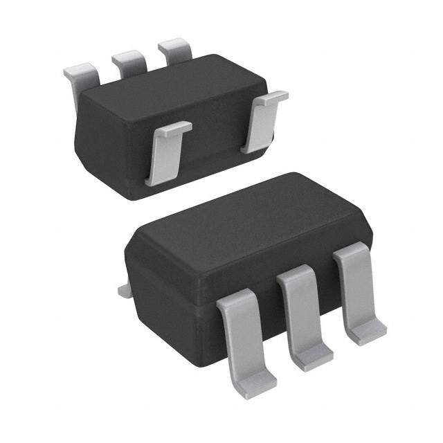
| 供应商器件封装 | SOT-23-5 |
| 元件数 | 1 |
| 其它名称 | 296-32293-2 |
| 包装 | 带卷 (TR) |
| 单位重量 | 15.800 mg |
| 商标 | Texas Instruments |
| 安装类型 | 表面贴装 |
| 安装风格 | SMD/SMT |
| 封装 | Reel |
| 封装/外壳 | SC-74A,SOT-753 |
| 封装/箱体 | SOT-23-5 |
| 工作温度 | -40°C ~ 125°C |
| 工厂包装数量 | 250 |
| 最大工作温度 | + 85 C |
| 最小工作温度 | - 40 C |
| 极性 | Non-Inverting |
| 标准包装 | 250 |
| 每元件位数 | 1 |
| 每芯片的通道数量 | 1 |
| 电压-电源 | 1.65 V ~ 5.5 V |
| 电流-输出高,低 | 32mA,32mA |
| 电源电压-最大 | 5.5 V |
| 电源电压-最小 | 1.65 V |
| 系列 | SN74LVC1G126 |
| 输入线路数量 | 1 |
| 输出类型 | 3-State |
| 输出线路数量 | 1 |
| 逻辑类型 | 缓冲器/线路驱动器,非反相 |
| 逻辑系列 | LVC |
| 配用 | /product-detail/zh/EV2300/296-18432-ND/809715 |
| 高电平输出电流 | - 32 mA |


PDF Datasheet 数据手册内容提取
Product Sample & Technical Tools & Support & Folder Buy Documents Software Community SN74LVC1G126 SCES224R–APRIL1999–REVISEDJANUARY2015 SN74LVC1G126 Single Bus Buffer Gate With 3-State Output 1 Features 2 Applications • AvailableintheTexasInstruments • CableModemTerminationSystems 1 NanoFree™Package • High-SpeedDataAcquisitionandGeneration • Supports5-VVCCOperation • Military:RadarsandSonars • InputsAcceptVoltagesto5.5V • MotorControls:High-Voltage • ProvidesDownTranslationtoVCC • PowerLineCommunicationModems • Maxtpdof3.7nsat3.3V • SSDs:InternalorExternal • LowPowerConsumption,10-μAMaxICC • VideoBroadcastingandInfrastructure:Scalable • ±24-mAOutputDriveat3.3V Platforms • I SupportsLiveInsertion,Partial-Power-Down • VideoBroadcasting:IP-BasedMulti-Format off Mode,andBackDriveProtection Transcoders • Latch-UpPerformanceExceeds100mA • VideoCommunicationSystems PerJESD78,ClassII 3 Description • ESDProtectionExceedsJESD22 This single buffer is designed for 1.65-V to 3.6-V V – 2000-VHuman-BodyModel CC operation. The LVC1G126 device is a single line – 200-VMachineModel driver with 3-state output. The output is disabled – 1000-VCharged-DeviceModel whentheoutput-enableinputislow. DeviceInformation(1) PARTNUMBER PACKAGE(PIN) BODYSIZE SOT-23(5) 2.90mm×1.60mm SC70(5) 2.00mm×1.25mm SN74LVC1G126 SOT(5) 1.60mm×1.20mm SON(6) 1.00mm×1.00mm XBGA(5) 1.40mm×0.90mm (1) For all available packages, see the orderable addendum at theendofthedatasheet. 4 Simplified Schematic 1 OE 2 4 A Y 1 An IMPORTANT NOTICE at the end of this data sheet addresses availability, warranty, changes, use in safety-critical applications, intellectualpropertymattersandotherimportantdisclaimers.PRODUCTIONDATA.
SN74LVC1G126 SCES224R–APRIL1999–REVISEDJANUARY2015 www.ti.com Table of Contents 1 Features.................................................................. 1 9 DetailedDescription............................................ 10 2 Applications........................................................... 1 9.1 Overview.................................................................10 3 Description............................................................. 1 9.2 FunctionalBlockDiagram.......................................10 4 SimplifiedSchematic............................................. 1 9.3 FeatureDescription.................................................10 9.4 DeviceFunctionalModes........................................10 5 RevisionHistory..................................................... 2 10 ApplicationandImplementation........................ 11 6 PinConfigurationandFunctions......................... 3 10.1 ApplicationInformation..........................................11 7 Specifications......................................................... 4 10.2 TypicalApplication ...............................................11 7.1 AbsoluteMaximumRatings .....................................4 11 PowerSupplyRecommendations..................... 12 7.2 ESDRatings..............................................................4 12 Layout................................................................... 12 7.3 RecommendedOperatingConditions......................5 7.4 ThermalInformation..................................................5 12.1 LayoutGuidelines.................................................12 7.5 ElectricalCharacteristics...........................................6 12.2 LayoutExample....................................................12 7.6 SwitchingCharacteristics,C =15pF......................6 13 DeviceandDocumentationSupport................. 13 L 7.7 SwitchingCharacteristics,–40°Cto85°C.................6 13.1 Trademarks...........................................................13 7.8 SwitchingCharacteristics,–40°Cto125°C...............7 13.2 ElectrostaticDischargeCaution............................13 7.9 OperatingCharacteristics........................................7 13.3 Glossary................................................................13 7.10 TypicalCharacteristics............................................7 14 Mechanical,Packaging,andOrderable Information........................................................... 13 8 ParameterMeasurementInformation..................8 5 Revision History ChangesfromRevisionQ(December2013)toRevisionR Page • AddedApplications,DeviceInformationtable,HandlingRatingstable,FeatureDescriptionsection,Device FunctionalModes,ApplicationandImplementationsection,PowerSupplyRecommendationssection,Layout section,DeviceandDocumentationSupportsection,andMechanical,Packaging,andOrderableInformationsection......1 ChangesfromRevisionP(November2012)toRevisionQ Page • UpdateddocumenttonewTIdatasheetformat.................................................................................................................... 1 • ChangedMAXoperatingtemperatureto125°CinRecommendedOperatingConditionstable. ......................................... 5 • AddedESDwarning............................................................................................................................................................. 13 ChangesfromRevisionO(March2011)toRevisionP Page • RemovedOrderingInformationtable..................................................................................................................................... 1 ChangesfromRevisionN(February2007)toRevisionO Page • AddedDSFpackageoptiontothedatasheet....................................................................................................................... 3 2 SubmitDocumentationFeedback Copyright©1999–2015,TexasInstrumentsIncorporated ProductFolderLinks:SN74LVC1G126
SN74LVC1G126 www.ti.com SCES224R–APRIL1999–REVISEDJANUARY2015 6 Pin Configuration and Functions DBV PACKAGE DCK PACKAGE DRLPACKAGE (TOPVIEW) (TOPVIEW) (TOPVIEW) OE 1 5 V OE 1 5 VCC OE 1 5 VCC CC A 2 A 2 GND 3 4 Y A 2 GND 3 4 Y GND 3 4 Y DRYPACKAGE DSF PACKAGE YZPPACKAGE (TOPVIEW) (TOPVIEW) (BOTTOM VIEW) OE 1 6 VCC OE 1 6 VCC GND C134C2 Y A 2 5 N.C. A 2 5 N.C. A B12 GND 3 4 Y GND 3 4 Y OE A115A2 VCC Seemechanicaldrawingsfordimensions. PinFunctions PIN SN74LVC1G126 TYPE DESCRIPTION NAME DBV,DCK, DRY,DSF DRL,YZP A 2 2 I AInput GND 3 3 — GroundPin NC — 5 — Donotconnect OE 1 1 I OEEnable/Input VCC 5 6 — PowerPin Y 4 4 O YOutput Copyright©1999–2015,TexasInstrumentsIncorporated SubmitDocumentationFeedback 3 ProductFolderLinks:SN74LVC1G126
SN74LVC1G126 SCES224R–APRIL1999–REVISEDJANUARY2015 www.ti.com 7 Specifications 7.1 Absolute Maximum Ratings overoperatingfree-airtemperaturerange(unlessotherwisenoted)(1) MIN MAX UNIT V Supplyvoltagerange –0.5 6.5 V CC V Inputvoltagerange(2) –0.5 6.5 V I V Voltagerangeappliedtoanyoutputinthehigh-impedanceorpower-offstate(2) –0.5 6.5 V O V Voltagerangeappliedtoanyoutputinthehighorlowstate(2)(3) –0.5 V +0.5 V O CC I Inputclampcurrent V <0 –50 mA IK I I Outputclampcurrent V <0 –50 mA OK O I Continuousoutputcurrent ±50 mA O ContinuouscurrentthroughV orGND ±100 mA CC T Storagetemperaturerange –65 150 °C stg (1) StressesbeyondthoselistedunderAbsoluteMaximumRatingsmaycausepermanentdamagetothedevice.Thesearestressratings only,andfunctionaloperationofthedeviceattheseoranyotherconditionsbeyondthoseindicatedunderRecommendedOperating Conditionsisnotimplied.Exposuretoabsolute-maximum-ratedconditionsforextendedperiodsmayaffectdevicereliability. (2) Theinputnegative-voltageandoutputvoltageratingsmaybeexceedediftheinputandoutputcurrentratingsareobserved. (3) ThevalueofV isprovidedintheRecommendedOperatingConditionstable. CC 7.2 ESD Ratings PARAMETER DEFINITION VALUE UNIT Electrostatic Humanbodymodel(HBM),perANSI/ESDA/JEDECJS-001,allpins(1) 2000 V V (ESD) discharge Chargeddevicemodel(CDM),perJEDECspecificationJESD22-C101,allpins(2) 1000 (1) JEDECdocumentJEP155statesthat500-VHBMallowssafemanufacturingwithastandardESDcontrolprocess. (2) JEDECdocumentJEP157statesthat250-VCDMallowssafemanufacturingwithastandardESDcontrolprocess. 4 SubmitDocumentationFeedback Copyright©1999–2015,TexasInstrumentsIncorporated ProductFolderLinks:SN74LVC1G126
SN74LVC1G126 www.ti.com SCES224R–APRIL1999–REVISEDJANUARY2015 7.3 Recommended Operating Conditions overoperatingfree-airtemperaturerange(unlessotherwisenoted)(1) MIN MAX UNIT Operating 1.65 5.5 V Supplyvoltage V CC Dataretentiononly 1.5 V =1.65Vto1.95V 0.65×V CC CC V =2.3Vto2.7V 1.7 CC V High-levelinputvoltage V IH V =3Vto3.6V 2 CC V =4.5Vto5.5V 0.7×V CC CC V =1.65Vto1.95V 0.35×V CC CC V =2.3Vto2.7V 0.7 CC V Low-levelinputvoltage V IL V =3Vto3.6V 0.8 CC V =4.5Vto5.5V 0.3×V CC CC V Inputvoltage 0 5.5 V I V Outputvoltage 0 V V O CC V =1.65V –4 CC V =2.3V –8 CC I High-leveloutputcurrent –16 mA OH V =3V CC –24 V =4.5V –32 CC V =1.65V 4 CC V =2.3V 8 CC I Low-leveloutputcurrent 16 mA OL V =3V CC 24 V =4.5V 32 CC V =1.8V±0.15V,2.5V±0.2V 20 CC Δt/Δv Inputtransitionriseorfallrate V =3.3V±0.3V 10 ns/V CC V =5V±0.5V 5 CC T Operatingfree-airtemperature –40 125 °C A (1) AllunusedinputsofthedevicemustbeheldatV orGNDtoensureproperdeviceoperation.RefertotheTIapplicationreport, CC ImplicationsofSloworFloatingCMOSInputs,literaturenumberSCBA004. 7.4 Thermal Information SN74LVC1G126 THERMALMETRIC(1) DBV DCK DRL DRY YZP UNIT 5PINS 5PINS 5PINS 6PINS 5PINS R Junction-to-ambientthermalresistance 206 252 142 234 132 °C/W θJA (1) Formoreinformationabouttraditionalandnewthermalmetrics,seetheICPackageThermalMetricsapplicationreport,SPRA953. Copyright©1999–2015,TexasInstrumentsIncorporated SubmitDocumentationFeedback 5 ProductFolderLinks:SN74LVC1G126
SN74LVC1G126 SCES224R–APRIL1999–REVISEDJANUARY2015 www.ti.com 7.5 Electrical Characteristics overrecommendedoperatingfree-airtemperaturerange(unlessotherwisenoted) –40°Cto85°C –40°Cto125°C PARAMETER TESTCONDITIONS VCC MIN TYP(1) MAX MIN TYP(1) MAX UNIT IOH=–100μA 1.65Vto5.5V VCC–0.1 VC0C.–1 IOH=–4mA 1.65V 1.2 1.2 VOH IOH=–8mA 2.3V 1.9 1.9 V IOH=–16mA 2.4 2.4 3V IOH=–24mA 2.3 2.3 IOH=–32mA 4.5V 3.8 3.8 IOL=100μA 1.65Vto5.5V 0.1 0.1 IOL=4mA 1.65V 0.45 0.45 IOL=8mA 2.3V 0.3 0.3 VOL V IOL=16mA 0.4 0.4 3V IOL=24mA 0.55 0.55 IOL=32mA 4.5V 0.55 0.55 AorOE II inputs VI=5.5VorGND 0to5.5V ±5 ±5 μA Ioff VIorVO=5.5V 0 ±10 ±10 μA IOZ VO=0to5.5V 3.6V 10 10 μA ICC VI=5.5VorGND IO=0 1.65Vto5.5V 10 10 μA ΔICC OOntheerinipnuptuatstaVtCVCCC–o0r.6GVN,D 3Vto5.5V 500 500 μA Ci VI=VCCorGND 3.3V 4 4 pF (1) AlltypicalvaluesareatV =3.3V,T =25°C. CC A 7.6 Switching Characteristics, C = 15 pF L overrecommendedoperatingfree-airtemperaturerange,C =15pF(unlessotherwisenoted)(seeFigure3) L –40°Cto85°C PARAMETER FROM TO VCC=1.8V VCC=2.5V VCC=3.3V VCC=5V UNIT (INPUT) (OUTPUT) ±0.15V ±0.2V ±0.3V ±0.5V MIN MAX MIN MAX MIN MAX MIN MAX tpd A Y 1.7 6.9 0.6 4.6 0.6 3.7 0.5 3.4 ns 7.7 Switching Characteristics, –40°C to 85°C overrecommendedoperatingfree-airtemperaturerange,C =30pFor50pF(unlessotherwisenoted)(seeFigure4) L –40°Cto85°C PARAMETER FROM TO VCC=1.8V VCC=2.5V VCC=3.3V VCC=5V UNIT (INPUT) (OUTPUT) ±0.15V ±0.2V ±0.3V ±0.5V MIN MAX MIN MAX MIN MAX MIN MAX tpd A Y 2.6 8 1.1 5.5 1 4.5 1 4 ns ten OE Y 2.8 9.4 1.3 6.6 1.2 5.3 1 5 ns tdis OE Y 1.6 9.8 1 5.5 1 5.5 1 4.2 ns 6 SubmitDocumentationFeedback Copyright©1999–2015,TexasInstrumentsIncorporated ProductFolderLinks:SN74LVC1G126
SN74LVC1G126 www.ti.com SCES224R–APRIL1999–REVISEDJANUARY2015 7.8 Switching Characteristics, –40°C to 125°C overrecommendedoperatingfree-airtemperaturerange,C =30pFor50pF(unlessotherwisenoted)(seeFigure4) L –40°Cto125°C PARAMETER FROM TO VCC=1.8V VCC=2.5V VCC=3.3V VCC=5V UNIT (INPUT) (OUTPUT) ±0.15V ±0.2V ±0.3V ±0.5V MIN MAX MIN MAX MIN MAX MIN MAX tpd A Y 2.6 9 1.1 5.7 1 4.7 1 4.2 ns ten OE Y 2.8 9.6 1.3 6.8 1.2 5.5 1 5.2 ns tdis OE Y 1.6 10 1 5.7 1 5.7 1 4.4 ns 7.9 Operating Characteristics T =25°C A TEST VCC=1.8V VCC=2.5V VCC=3.3V VCC=5V PARAMETER UNIT CONDITIONS TYP TYP TYP TYP Powerdissipation Outputsenabled 19 19 19 21 Cpd capacitance Outputsdisabled f=10MHz 2 2 3 4 pF 7.10 Typical Characteristics 14 10 VCC=3V, VCC=3V, TA=25°C TA=25°C 12 s –ns OneOutputSwitching e–n 8 OneOutputSwitching e m Tim 10 yTi y a ela Del D 8 n 6 n o atio gati g a a 6 p p o o r Pr –P 4 – d d 4 p p t t 2 2 0 50 100 150 200 250 300 0 50 100 150 200 250 300 CL–LoadCapacitance–pF CL–LoadCapacitance–pF Figure1.PropagationDelay(LowtoHighTransition) Figure2.PropagationDelay(HightoLowTransition) vsLoadCapacitance vsLoadCapacitance Copyright©1999–2015,TexasInstrumentsIncorporated SubmitDocumentationFeedback 7 ProductFolderLinks:SN74LVC1G126
SN74LVC1G126 SCES224R–APRIL1999–REVISEDJANUARY2015 www.ti.com 8 Parameter Measurement Information VLOAD From Output RL S1 Open TEST S1 Under Test GND tPLH/tPHL Open (see NoteCAL) RL tPLZ/tPZL VLOAD tPHZ/tPZH GND LOAD CIRCUIT INPUTS VCC VI tr/tf VM VLOAD CL RL V∆ 1.8 V±0.15 V VCC ≤2ns VCC/2 2×VCC 15 pF 1 MΩ 0.15 V 2.5 V±0.2 V VCC ≤2ns VCC/2 2×VCC 15 pF 1 MΩ 0.15 V 3.3 V±0.3 V 3 V ≤2.5 ns 1.5 V 6 V 15 pF 1 MΩ 0.3 V 5V±0.5 V VCC ≤2.5 ns VCC/2 2×VCC 15 pF 1 MΩ 0.3 V VI Timing Input VM 0 V tw VI tsu th VI Input VM VM Data Input VM VM 0 V 0 V VOLTAGEWAVEFORMS VOLTAGEWAVEFORMS PULSEDURATION SETUPAND HOLD TIMES VI VI Output Input VM VM Control VM VM 0 V 0 V tPLH tPHL tPZL tPLZ Output VOH Waveform 1 VLOAD/2 Output VM VM VOL (Ss1ee a tN VoLteO ABD) VM VOL+V∆ VOL tPHL tPLH tPZH tPHZ Output VM VM VOH WSa1v eaOftou GrtmpNu D2t VM VOH−V∆ VOH VOL (see Note B) ≈0 V VOLTAGEWAVEFORMS VOLTAGEWAVEFORMS PROPAGATIONDELAYTIMES ENABLEAND DISABLE TIMES INVERTINGAND NONINVERTING OUTPUTS LOW-ANDHIGH-LEVELENABLING NOTES: A. CLincludes probe and jig capacitance. B. Waveform1isforanoutputwithinternalconditionssuchthattheoutputislow,exceptwhendisabledbytheoutputcontrol. Waveform2is for an output with internal conditions such that the output is high, except when disabled by the output control. C. All input pulses are supplied by generators having the following characteristics: PRR≤10 MHz, ZO= 50Ω. D. The outputs are measured one at a time, with one transition per measurement. E. tPLZand tPHZare the same as tdis. F. tPZLand tPZHare the same as ten. G. tPLHand tPHLare the same as tpd. H. All parameters and waveforms are not applicable to all devices. Figure3. LoadCircuitandVoltageWaveforms 8 SubmitDocumentationFeedback Copyright©1999–2015,TexasInstrumentsIncorporated ProductFolderLinks:SN74LVC1G126
SN74LVC1G126 www.ti.com SCES224R–APRIL1999–REVISEDJANUARY2015 Parameter Measurement Information (continued) VLOAD From Output RL S1 Open TEST S1 Under Test GND tPLH/tPHL Open (see NoteCAL) RL tPLZ/tPZL VLOAD tPHZ/tPZH GND LOAD CIRCUIT INPUTS VCC VI tr/tf VM VLOAD CL RL V∆ 1.8 V±0.15 V VCC ≤2ns VCC/2 2×VCC 30 pF 1 kΩ 0.15 V 2.5 V±0.2 V VCC ≤2ns VCC/2 2×VCC 30 pF 500Ω 0.15 V 3.3 V±0.3 V 3 V ≤2.5 ns 1.5 V 6 V 50 pF 500Ω 0.3 V 5V±0.5 V VCC ≤2.5 ns VCC/2 2×VCC 50 pF 500Ω 0.3 V VI Timing Input VM 0 V tw VI tsu th VI Input VM VM Data Input VM VM 0 V 0 V VOLTAGEWAVEFORMS VOLTAGEWAVEFORMS PULSEDURATION SETUPAND HOLD TIMES VI VI Output Input VM VM Control VM VM 0 V 0 V tPLH tPHL tPZL tPLZ Output VOH Waveform 1 VLOAD/2 Output VM VM VOL (Ss1ee a tN VoLteO ABD) VM VOL+V∆ VOL tPHL tPLH tPZH tPHZ Output VM VM VOH WSa1v eaOftou GrtmpNu D2t VM VOH−V∆ VOH VOL (see Note B) ≈0 V VOLTAGEWAVEFORMS VOLTAGEWAVEFORMS PROPAGATIONDELAYTIMES ENABLEAND DISABLE TIMES INVERTINGAND NONINVERTING OUTPUTS LOW-ANDHIGH-LEVELENABLING NOTES: A. CLincludes probe and jig capacitance. B. Waveform1isforanoutputwithinternalconditionssuchthattheoutputislow,exceptwhendisabledbytheoutputcontrol. Waveform2is for an output with internal conditions such that the output is high, except when disabled by the output control. C. All input pulses are supplied by generators having the following characteristics: PRR≤10 MHz, ZO= 50Ω. D. The outputs are measured one at a time, with one transition per measurement. E. tPLZand tPHZare the same as tdis. F. tPZLand tPZHare the same as ten. G. tPLHand tPHLare the same as tpd. H. All parameters and waveforms are not applicable to all devices. Figure4. LoadCircuitandVoltageWaveforms Copyright©1999–2015,TexasInstrumentsIncorporated SubmitDocumentationFeedback 9 ProductFolderLinks:SN74LVC1G126
SN74LVC1G126 SCES224R–APRIL1999–REVISEDJANUARY2015 www.ti.com 9 Detailed Description 9.1 Overview The SN74LVC1G126 device contains a dual buffer gate with output enable control and performs the Boolean functionY=A. This device is fully specified for partial-power-down applications using I . The I circuitry disables the outputs, off off preventingdamagingcurrentbackflowthroughthedevicewhenitispowereddown. To ensure the high-impedance state during power up or power down, OE should be tied to GND through a pull- downresistor;theminimumvalueoftheresistorisdeterminedbythecurrent-sourcingcapabilityofthedriver. 9.2 Functional Block Diagram 1 OE 2 4 A Y 9.3 Feature Description • 1.65Vto5.5Voperatingvoltagerange • Allowsdownvoltagetranslation – 5Vto3.3V – 5Vor3.3Vto1.8V • Inputsacceptvoltagesto5.5V – 5.5-VtoleranceoninputpinwhenV =0V CC • I feature off – AllowsvoltageontheinputsandoutputswhenV is0V CC – AbletoreduceleakagewhenV is0V CC 9.4 Device Functional Modes Table1.FunctionTable INPUTS OUTPUT OE A Y H H H H L L L X Z 10 SubmitDocumentationFeedback Copyright©1999–2015,TexasInstrumentsIncorporated ProductFolderLinks:SN74LVC1G126
SN74LVC1G126 www.ti.com SCES224R–APRIL1999–REVISEDJANUARY2015 10 Application and Implementation NOTE Information in the following applications sections is not part of the TI component specification, and TI does not warrant its accuracy or completeness. TI’s customers are responsible for determining suitability of components for their purposes. Customers should validateandtesttheirdesignimplementationtoconfirmsystemfunctionality. 10.1 Application Information The SN74LVC1G126 device is a high-drive CMOS device that can be used as an output enabled buffer with a high output drive, such as an LED application. It can produce 24 mA of drive current at 3.3 V, making it ideal for driving multiple outputs and good for high speed applications up to 100 MHz. The inputs are 5.5-V tolerant allowingittotranslatedowntoV . CC 10.2 Typical Application 1.65 V to 5 V SN74LVC1G126 0.1 PF OE VCC Input signal 1 A from system Output 1 to long GND Y PCB trace or high-Z logic input Figure5. ApplicationSchematic 10.2.1 DesignRequirements This device uses CMOS technology and has balanced output drive. Care should be taken to avoid bus contention because it can drive currents that would exceed maximum limits. Outputs can be combined to produce higher drive but the high drive will also create faster edges into light loads, so routing and load conditionsshouldbeconsideredtopreventringing. 10.2.2 DetailedDesignProcedure 1. RecommendedInputConditions: – Forrisetimeandfalltimespecifications,see Δt/ΔVintheRecommendedOperatingConditions table. – Forspecifiedhighandlowlevels,seeV andV intheRecommendedOperatingConditions table. IH IL – Inputsareovervoltagetolerantallowingthemtogoashighas5.5VatanyvalidV . CC 2. RecommendOutputConditions: – Loadcurrentsshouldnotexceed50mAperoutputand100mAtotalforthepart. Copyright©1999–2015,TexasInstrumentsIncorporated SubmitDocumentationFeedback 11 ProductFolderLinks:SN74LVC1G126
SN74LVC1G126 SCES224R–APRIL1999–REVISEDJANUARY2015 www.ti.com Typical Application (continued) 10.2.3 ApplicationCurves 10 V 1.8 V 9 VCC2.5 V CC 8 VCC3.3 V V 5 V CC 7 A) 6 m ( 5 C IC 4 3 2 1 0 0 20 40 60 80 Frequency(MHz) D003 Figure6.I vsFrequency CC 11 Power Supply Recommendations The power supply can be any voltage between the MIN and MAX supply voltage rating located in the RecommendedOperatingConditionstable. Each V terminal should have a good bypass capacitor to prevent power disturbance. For devices with a single CC supply, a 0.1-μF capacitor is recommended. If there are multiple V terminals, then 0.01-μF or 0.022-μF CC capacitors are recommended for each power terminal. It is ok to parallel multiple bypass capacitors to reject different frequencies of noise. Multiple bypass capacitors may be paralleled to reject different frequencies of noise.Thebypasscapacitorshouldbeinstalledasclosetothepowerterminalaspossibleforthebestresults. 12 Layout 12.1 Layout Guidelines When using multiple bit logic devices, inputs should not float. In many cases, functions or parts of functions of digital logic devices are unused. Some examples are when only two inputs of a triple-input AND gate are used, or when only 3 of the 4-buffer gates are used. Such input pins should not be left unconnected because the undefinedvoltagesattheoutsideconnectionsresultinundefinedoperationalstates. Specified in Figure 7 are rules that must be observed under all circumstances. All unused inputs of digital logic devices must be connected to a high or low bias to prevent them from floating. The logic level that should be applied to any particular unused input depends on the function of the device. Generally they will be tied to GND or V , whichever makes more sense or is more convenient. It is acceptable to float outputs unless the part is a CC transceiver. If the transceiver has an output enable pin, it will disable the outputs section of the part when asserted.ThiswillnotdisabletheinputsectionoftheI/Ossotheyalsocannotfloatwhendisabled. 12.2 Layout Example V cc Input Unused Input Output Unused Input Output Input Figure7. LayoutDiagram 12 SubmitDocumentationFeedback Copyright©1999–2015,TexasInstrumentsIncorporated ProductFolderLinks:SN74LVC1G126
SN74LVC1G126 www.ti.com SCES224R–APRIL1999–REVISEDJANUARY2015 13 Device and Documentation Support 13.1 Trademarks NanoFreeisatrademarkofTexasInstruments. Allothertrademarksarethepropertyoftheirrespectiveowners. 13.2 Electrostatic Discharge Caution Thesedeviceshavelimitedbuilt-inESDprotection.Theleadsshouldbeshortedtogetherorthedeviceplacedinconductivefoam duringstorageorhandlingtopreventelectrostaticdamagetotheMOSgates. 13.3 Glossary SLYZ022—TIGlossary. Thisglossarylistsandexplainsterms,acronymsanddefinitions. 14 Mechanical, Packaging, and Orderable Information The following pages include mechanical packaging and orderable information. This information is the most current data available for the designated devices. This data is subject to change without notice and revision of thisdocument.Forbrowserbasedversionsofthisdatasheet,refertothelefthandnavigation. Copyright©1999–2015,TexasInstrumentsIncorporated SubmitDocumentationFeedback 13 ProductFolderLinks:SN74LVC1G126
PACKAGE OPTION ADDENDUM www.ti.com 4-Apr-2019 PACKAGING INFORMATION Orderable Device Status Package Type Package Pins Package Eco Plan Lead/Ball Finish MSL Peak Temp Op Temp (°C) Device Marking Samples (1) Drawing Qty (2) (6) (3) (4/5) 74LVC1G126DBVRE4 ACTIVE SOT-23 DBV 5 3000 Green (RoHS CU NIPDAU Level-1-260C-UNLIM -40 to 125 C26F & no Sb/Br) 74LVC1G126DBVRG4 ACTIVE SOT-23 DBV 5 3000 Green (RoHS CU NIPDAU Level-1-260C-UNLIM -40 to 125 C26F & no Sb/Br) 74LVC1G126DBVTE4 ACTIVE SOT-23 DBV 5 250 Green (RoHS CU NIPDAU Level-1-260C-UNLIM -40 to 125 C26F & no Sb/Br) 74LVC1G126DBVTG4 ACTIVE SOT-23 DBV 5 250 Green (RoHS CU NIPDAU Level-1-260C-UNLIM -40 to 125 C26F & no Sb/Br) 74LVC1G126DCKRE4 ACTIVE SC70 DCK 5 3000 Green (RoHS CU NIPDAU Level-1-260C-UNLIM -40 to 125 CN5 & no Sb/Br) 74LVC1G126DCKRG4 ACTIVE SC70 DCK 5 3000 Green (RoHS CU NIPDAU Level-1-260C-UNLIM -40 to 125 CN5 & no Sb/Br) 74LVC1G126DCKTG4 ACTIVE SC70 DCK 5 250 Green (RoHS CU NIPDAU Level-1-260C-UNLIM -40 to 125 CN5 & no Sb/Br) 74LVC1G126DRLRG4 ACTIVE SOT-5X3 DRL 5 4000 Green (RoHS CU NIPDAU Level-1-260C-UNLIM -40 to 125 (CN7, CNR) & no Sb/Br) SN74LVC1G126DBVR ACTIVE SOT-23 DBV 5 3000 Green (RoHS CU NIPDAU | CU SN Level-1-260C-UNLIM -40 to 125 (C265, C26F, C26J, & no Sb/Br) C26K, C26R, C 26T) SN74LVC1G126DBVT ACTIVE SOT-23 DBV 5 250 Green (RoHS CU NIPDAU | CU SN Level-1-260C-UNLIM -40 to 125 (C265, C26F, C26J, & no Sb/Br) C26K, C26R) SN74LVC1G126DCKR ACTIVE SC70 DCK 5 3000 Green (RoHS CU NIPDAU | CU SN Level-1-260C-UNLIM -40 to 125 (CN5, CNF, CNJ, CN & no Sb/Br) K, CNR, CNT) SN74LVC1G126DCKT ACTIVE SC70 DCK 5 250 Green (RoHS CU NIPDAU | CU SN Level-1-260C-UNLIM -40 to 125 (CN5, CNF, CNJ, CN & no Sb/Br) K, CNR) SN74LVC1G126DRLR ACTIVE SOT-5X3 DRL 5 4000 Green (RoHS CU NIPDAU | Level-1-260C-UNLIM -40 to 125 (CN7, CNR) & no Sb/Br) CU NIPDAUAG SN74LVC1G126DRYR ACTIVE SON DRY 6 5000 Green (RoHS CU NIPDAU Level-1-260C-UNLIM -40 to 125 CN & no Sb/Br) SN74LVC1G126DSFR ACTIVE SON DSF 6 5000 Green (RoHS CU NIPDAU Level-1-260C-UNLIM -40 to 125 CN & no Sb/Br) SN74LVC1G126YZPR ACTIVE DSBGA YZP 5 3000 Green (RoHS SNAGCU Level-1-260C-UNLIM -40 to 85 (CN7, CNN) & no Sb/Br) (1) The marketing status values are defined as follows: Addendum-Page 1
PACKAGE OPTION ADDENDUM www.ti.com 4-Apr-2019 ACTIVE: Product device recommended for new designs. LIFEBUY: TI has announced that the device will be discontinued, and a lifetime-buy period is in effect. NRND: Not recommended for new designs. Device is in production to support existing customers, but TI does not recommend using this part in a new design. PREVIEW: Device has been announced but is not in production. Samples may or may not be available. OBSOLETE: TI has discontinued the production of the device. (2) RoHS: TI defines "RoHS" to mean semiconductor products that are compliant with the current EU RoHS requirements for all 10 RoHS substances, including the requirement that RoHS substance do not exceed 0.1% by weight in homogeneous materials. Where designed to be soldered at high temperatures, "RoHS" products are suitable for use in specified lead-free processes. TI may reference these types of products as "Pb-Free". RoHS Exempt: TI defines "RoHS Exempt" to mean products that contain lead but are compliant with EU RoHS pursuant to a specific EU RoHS exemption. Green: TI defines "Green" to mean the content of Chlorine (Cl) and Bromine (Br) based flame retardants meet JS709B low halogen requirements of <=1000ppm threshold. Antimony trioxide based flame retardants must also meet the <=1000ppm threshold requirement. (3) MSL, Peak Temp. - The Moisture Sensitivity Level rating according to the JEDEC industry standard classifications, and peak solder temperature. (4) There may be additional marking, which relates to the logo, the lot trace code information, or the environmental category on the device. (5) Multiple Device Markings will be inside parentheses. Only one Device Marking contained in parentheses and separated by a "~" will appear on a device. If a line is indented then it is a continuation of the previous line and the two combined represent the entire Device Marking for that device. (6) Lead/Ball Finish - Orderable Devices may have multiple material finish options. Finish options are separated by a vertical ruled line. Lead/Ball Finish values may wrap to two lines if the finish value exceeds the maximum column width. Important Information and Disclaimer:The information provided on this page represents TI's knowledge and belief as of the date that it is provided. TI bases its knowledge and belief on information provided by third parties, and makes no representation or warranty as to the accuracy of such information. Efforts are underway to better integrate information from third parties. TI has taken and continues to take reasonable steps to provide representative and accurate information but may not have conducted destructive testing or chemical analysis on incoming materials and chemicals. TI and TI suppliers consider certain information to be proprietary, and thus CAS numbers and other limited information may not be available for release. In no event shall TI's liability arising out of such information exceed the total purchase price of the TI part(s) at issue in this document sold by TI to Customer on an annual basis. OTHER QUALIFIED VERSIONS OF SN74LVC1G126 : •Automotive: SN74LVC1G126-Q1 •Enhanced Product: SN74LVC1G126-EP NOTE: Qualified Version Definitions: •Automotive - Q100 devices qualified for high-reliability automotive applications targeting zero defects Addendum-Page 2
PACKAGE OPTION ADDENDUM www.ti.com 4-Apr-2019 •Enhanced Product - Supports Defense, Aerospace and Medical Applications Addendum-Page 3
PACKAGE MATERIALS INFORMATION www.ti.com 15-Feb-2019 TAPE AND REEL INFORMATION *Alldimensionsarenominal Device Package Package Pins SPQ Reel Reel A0 B0 K0 P1 W Pin1 Type Drawing Diameter Width (mm) (mm) (mm) (mm) (mm) Quadrant (mm) W1(mm) 74LVC1G126DBVRG4 SOT-23 DBV 5 3000 178.0 9.0 3.23 3.17 1.37 4.0 8.0 Q3 74LVC1G126DBVTG4 SOT-23 DBV 5 250 178.0 9.0 3.23 3.17 1.37 4.0 8.0 Q3 74LVC1G126DCKRG4 SC70 DCK 5 3000 178.0 9.2 2.4 2.4 1.22 4.0 8.0 Q3 74LVC1G126DCKTG4 SC70 DCK 5 250 178.0 9.2 2.4 2.4 1.22 4.0 8.0 Q3 SN74LVC1G126DBVR SOT-23 DBV 5 3000 178.0 9.0 3.23 3.17 1.37 4.0 8.0 Q3 SN74LVC1G126DBVR SOT-23 DBV 5 3000 180.0 8.4 3.23 3.17 1.37 4.0 8.0 Q3 SN74LVC1G126DBVR SOT-23 DBV 5 3000 178.0 9.2 3.3 3.23 1.55 4.0 8.0 Q3 SN74LVC1G126DBVR SOT-23 DBV 5 3000 178.0 9.0 3.3 3.2 1.4 4.0 8.0 Q3 SN74LVC1G126DBVT SOT-23 DBV 5 250 178.0 9.0 3.23 3.17 1.37 4.0 8.0 Q3 SN74LVC1G126DBVT SOT-23 DBV 5 250 178.0 9.2 3.3 3.23 1.55 4.0 8.0 Q3 SN74LVC1G126DBVT SOT-23 DBV 5 250 178.0 9.0 3.3 3.2 1.4 4.0 8.0 Q3 SN74LVC1G126DCKR SC70 DCK 5 3000 178.0 9.2 2.4 2.4 1.22 4.0 8.0 Q3 SN74LVC1G126DCKT SC70 DCK 5 250 180.0 9.2 2.3 2.55 1.2 4.0 8.0 Q3 SN74LVC1G126DCKT SC70 DCK 5 250 178.0 9.0 2.4 2.5 1.2 4.0 8.0 Q3 SN74LVC1G126DCKT SC70 DCK 5 250 178.0 9.2 2.4 2.4 1.22 4.0 8.0 Q3 SN74LVC1G126DCKT SC70 DCK 5 250 178.0 9.0 2.4 2.5 1.2 4.0 8.0 Q3 SN74LVC1G126DRLR SOT-5X3 DRL 5 4000 180.0 9.5 1.78 1.78 0.69 4.0 8.0 Q3 SN74LVC1G126DRLR SOT-5X3 DRL 5 4000 180.0 8.4 1.98 1.78 0.69 4.0 8.0 Q3 PackMaterials-Page1
PACKAGE MATERIALS INFORMATION www.ti.com 15-Feb-2019 Device Package Package Pins SPQ Reel Reel A0 B0 K0 P1 W Pin1 Type Drawing Diameter Width (mm) (mm) (mm) (mm) (mm) Quadrant (mm) W1(mm) SN74LVC1G126DRYR SON DRY 6 5000 179.0 8.4 1.2 1.65 0.7 4.0 8.0 Q1 SN74LVC1G126DSFR SON DSF 6 5000 180.0 9.5 1.16 1.16 0.5 4.0 8.0 Q2 SN74LVC1G126YZPR DSBGA YZP 5 3000 178.0 9.2 1.02 1.52 0.63 4.0 8.0 Q1 *Alldimensionsarenominal Device PackageType PackageDrawing Pins SPQ Length(mm) Width(mm) Height(mm) 74LVC1G126DBVRG4 SOT-23 DBV 5 3000 180.0 180.0 18.0 74LVC1G126DBVTG4 SOT-23 DBV 5 250 180.0 180.0 18.0 74LVC1G126DCKRG4 SC70 DCK 5 3000 180.0 180.0 18.0 74LVC1G126DCKTG4 SC70 DCK 5 250 180.0 180.0 18.0 SN74LVC1G126DBVR SOT-23 DBV 5 3000 180.0 180.0 18.0 SN74LVC1G126DBVR SOT-23 DBV 5 3000 202.0 201.0 28.0 SN74LVC1G126DBVR SOT-23 DBV 5 3000 180.0 180.0 18.0 SN74LVC1G126DBVR SOT-23 DBV 5 3000 180.0 180.0 18.0 SN74LVC1G126DBVT SOT-23 DBV 5 250 180.0 180.0 18.0 SN74LVC1G126DBVT SOT-23 DBV 5 250 180.0 180.0 18.0 SN74LVC1G126DBVT SOT-23 DBV 5 250 180.0 180.0 18.0 SN74LVC1G126DCKR SC70 DCK 5 3000 180.0 180.0 18.0 SN74LVC1G126DCKT SC70 DCK 5 250 205.0 200.0 33.0 SN74LVC1G126DCKT SC70 DCK 5 250 180.0 180.0 18.0 PackMaterials-Page2
PACKAGE MATERIALS INFORMATION www.ti.com 15-Feb-2019 Device PackageType PackageDrawing Pins SPQ Length(mm) Width(mm) Height(mm) SN74LVC1G126DCKT SC70 DCK 5 250 180.0 180.0 18.0 SN74LVC1G126DCKT SC70 DCK 5 250 180.0 180.0 18.0 SN74LVC1G126DRLR SOT-5X3 DRL 5 4000 184.0 184.0 19.0 SN74LVC1G126DRLR SOT-5X3 DRL 5 4000 202.0 201.0 28.0 SN74LVC1G126DRYR SON DRY 6 5000 203.0 203.0 35.0 SN74LVC1G126DSFR SON DSF 6 5000 184.0 184.0 19.0 SN74LVC1G126YZPR DSBGA YZP 5 3000 220.0 220.0 35.0 PackMaterials-Page3
PACKAGE OUTLINE YZP0005 DSBGA - 0.5 mm max height SCALE 8.000 DIE SIZE BALL GRID ARRAY B E A BALL A1 CORNER D C 0.5 MAX SEATING PLANE 0.19 0.05 C 0.15 BALL TYP 0.5 TYP C SYMM 1 B D: Max = 1.44 mm, Min = 1.38 mm TYP 0.5 TYP E: Max = 0.94 mm, Min = 0.88 mm A 0.25 5X 1 2 0.21 0.015 C A B SYMM 4219492/A 05/2017 NOTES: 1. All linear dimensions are in millimeters. Any dimensions in parenthesis are for reference only. Dimensioning and tolerancing per ASME Y14.5M. 2. This drawing is subject to change without notice. www.ti.com
EXAMPLE BOARD LAYOUT YZP0005 DSBGA - 0.5 mm max height DIE SIZE BALL GRID ARRAY (0.5) TYP 5X ( 0.23) 1 2 A (0.5) TYP SYMM B C SYMM LAND PATTERN EXAMPLE SCALE:40X SOLDER MASK 0.05 MAX 0.05 MIN ( 0.23) OPENING SOLDER MASK OPENING ( 0.23) METAL METAL UNDER SOLDER MASK NON-SOLDER MASK SOLDER MASK DEFINED DEFINED (PREFERRED) SOLDER MASK DETAILS NOT TO SCALE 4219492/A 05/2017 NOTES: (continued) 3. Final dimensions may vary due to manufacturing tolerance considerations and also routing constraints. For more information, see Texas Instruments literature number SNVA009 (www.ti.com/lit/snva009). www.ti.com
EXAMPLE STENCIL DESIGN YZP0005 DSBGA - 0.5 mm max height DIE SIZE BALL GRID ARRAY (0.5) TYP 5X ( 0.25) (R0.05) TYP 1 2 A (0.5) TYP B SYMM C METAL SYMM TYP SOLDER PASTE EXAMPLE BASED ON 0.1 mm THICK STENCIL SCALE:40X 4219492/A 05/2017 NOTES: (continued) 4. Laser cutting apertures with trapezoidal walls and rounded corners may offer better paste release. www.ti.com
None
None
PACKAGE OUTLINE DSF0006A X2SON - 0.4 mm max height SCALE 10.000 PLASTIC SMALL OUTLINE - NO LEAD 1.05 B A 0.95 PIN 1 INDEX AREA 1.05 0.95 0.4 MAX C SEATING PLANE 0.05 C (0.11) TYP SYMM 0.05 0.00 3 4 2X SYMM 0.7 4X 0.35 6 1 0.22 6X 0.12 (0.1) PIN 1 ID 0.45 0.07 C B A 6X 0.35 0.05 C 4220597/A 06/2017 NOTES: 1. All linear dimensions are in millimeters. Any dimensions in parenthesis are for reference only. Dimensioning and tolerancing per ASME Y14.5M. 2. This drawing is subject to change without notice. 3. Reference JEDEC registration MO-287, variation X2AAF. www.ti.com
EXAMPLE BOARD LAYOUT DSF0006A X2SON - 0.4 mm max height PLASTIC SMALL OUTLINE - NO LEAD 6X (0.6) (R0.05) TYP 1 6X (0.17) 6 SYMM 4X (0.35) 4 3 SYMM (0.8) LAND PATTERN EXAMPLE EXPOSED METAL SHOWN SCALE:40X 0.07 MIN 0.07 MAX EXPOSED METAL ALL AROUND ALL AROUND EXPOSED METAL SOLDER MASK SOLDER MASK METAL METAL UNDER OPENING OPENING SOLDER MASK NON SOLDER MASK SOLDER MASK DEFINED DEFINED SOLDER MASK DETAILS 4220597/A 06/2017 NOTES: (continued) 4. For more information, see Texas Instruments literature number SLUA271 (www.ti.com/lit/slua271). www.ti.com
EXAMPLE STENCIL DESIGN DSF0006A X2SON - 0.4 mm max height PLASTIC SMALL OUTLINE - NO LEAD 6X (0.6) (R0.05) TYP 1 6X (0.17) 6 SYMM 4X (0.35) 4 3 SYMM (0.8) SOLDER PASTE EXAMPLE BASED ON 0.125 mm THICK STENCIL PRINTED SOLDER COVERAGE BY AREA UNDER PACKAGE SCALE:40X 4220597/A 06/2017 4. Laser cutting apertures with trapezoidal walls and rounded corners may offer better paste release. IPC-7525 may have alternate design recommendations. www.ti.com
PACKAGE OUTLINE DBV0005A SOT-23 - 1.45 mm max height SCALE 4.000 SMALL OUTLINE TRANSISTOR C 3.0 2.6 0.1 C 1.75 1.45 B A 1.45 MAX PIN 1 INDEX AREA 1 5 2X 0.95 3.05 2.75 1.9 1.9 2 4 3 0.5 5X 0.3 0.15 0.2 C A B (1.1) TYP 0.00 0.25 GAGE PLANE 0.22 TYP 0.08 8 TYP 0.6 0 0.3 TYP SEATING PLANE 4214839/D 11/2018 NOTES: 1. All linear dimensions are in millimeters. Any dimensions in parenthesis are for reference only. Dimensioning and tolerancing per ASME Y14.5M. 2. This drawing is subject to change without notice. 3. Refernce JEDEC MO-178. 4. Body dimensions do not include mold flash, protrusions, or gate burrs. Mold flash, protrusions, or gate burrs shall not exceed 0.15 mm per side. www.ti.com
EXAMPLE BOARD LAYOUT DBV0005A SOT-23 - 1.45 mm max height SMALL OUTLINE TRANSISTOR PKG 5X (1.1) 1 5 5X (0.6) SYMM (1.9) 2 2X (0.95) 3 4 (R0.05) TYP (2.6) LAND PATTERN EXAMPLE EXPOSED METAL SHOWN SCALE:15X SOLDER MASK SOLDER MASK METAL UNDER METAL OPENING OPENING SOLDER MASK EXPOSED METAL EXPOSED METAL 0.07 MAX 0.07 MIN ARROUND ARROUND NON SOLDER MASK SOLDER MASK DEFINED DEFINED (PREFERRED) SOLDER MASK DETAILS 4214839/D 11/2018 NOTES: (continued) 5. Publication IPC-7351 may have alternate designs. 6. Solder mask tolerances between and around signal pads can vary based on board fabrication site. www.ti.com
EXAMPLE STENCIL DESIGN DBV0005A SOT-23 - 1.45 mm max height SMALL OUTLINE TRANSISTOR PKG 5X (1.1) 1 5 5X (0.6) SYMM 2 (1.9) 2X(0.95) 3 4 (R0.05) TYP (2.6) SOLDER PASTE EXAMPLE BASED ON 0.125 mm THICK STENCIL SCALE:15X 4214839/D 11/2018 NOTES: (continued) 7. Laser cutting apertures with trapezoidal walls and rounded corners may offer better paste release. IPC-7525 may have alternate design recommendations. 8. Board assembly site may have different recommendations for stencil design. www.ti.com
None
None
GENERIC PACKAGE VIEW DRY 6 USON - 0.6 mm max height PLASTIC SMALL OUTLINE - NO LEAD Images above are just a representation of the package family, actual package may vary. Refer to the product data sheet for package details. 4207181/G
PACKAGE OUTLINE DRY0006A USON - 0.6 mm max height SCALE 8.500 PLASTIC SMALL OUTLINE - NO LEAD B 1.05 A 0.95 PIN 1 INDEX AREA 1.5 1.4 0.6 MAX C SEATING PLANE 0.05 0.00 0.08 C 3X 0.6 SYMM (0.127) TYP (0.05) TYP 3 4 4X 0.5 SYMM 2X 1 6 1 0.25 6X 0.15 0.4 0.3 0.1 C A B 0.05 C PIN 1 ID (OPTIONAL) 0.35 5X 0.25 4222894/A 01/2018 NOTES: 1. All linear dimensions are in millimeters. Any dimensions in parenthesis are for reference only. Dimensioning and tolerancing per ASME Y14.5M. 2. This drawing is subject to change without notice. www.ti.com
EXAMPLE BOARD LAYOUT DRY0006A USON - 0.6 mm max height PLASTIC SMALL OUTLINE - NO LEAD SYMM (0.35) 5X (0.3) 1 6 6X (0.2) SYMM 4X (0.5) 4 3 (R0.05) TYP (0.6) LAND PATTERN EXAMPLE 1:1 RATIO WITH PKG SOLDER PADS EXPOSED METAL SHOWN SCALE:40X 0.05 MAX 0.05 MIN ALL AROUND ALL AROUND EXPOSED EXPOSED METAL METAL SOLDER MASK METAL METAL UNDER SOLDER MASK OPENING SOLDER MASK OPENING NON SOLDER MASK DEFINED SOLDER MASK DEFINED (PREFERRED) SOLDER MASK DETAILS 4222894/A 01/2018 NOTES: (continued) 3. For more information, see QFN/SON PCB application report in literature No. SLUA271 (www.ti.com/lit/slua271). www.ti.com
EXAMPLE STENCIL DESIGN DRY0006A USON - 0.6 mm max height PLASTIC SMALL OUTLINE - NO LEAD SYMM (0.35) 5X (0.3) 1 6 6X (0.2) SYMM 4X (0.5) 4 3 (R0.05) TYP (0.6) SOLDER PASTE EXAMPLE BASED ON 0.075 - 0.1 mm THICK STENCIL SCALE:40X 4222894/A 01/2018 NOTES: (continued) 4. Laser cutting apertures with trapezoidal walls and rounded corners may offer better paste release. IPC-7525 may have alternate design recommendations. www.ti.com
IMPORTANTNOTICEANDDISCLAIMER TIPROVIDESTECHNICALANDRELIABILITYDATA(INCLUDINGDATASHEETS),DESIGNRESOURCES(INCLUDINGREFERENCE DESIGNS),APPLICATIONOROTHERDESIGNADVICE,WEBTOOLS,SAFETYINFORMATION,ANDOTHERRESOURCES“ASIS” ANDWITHALLFAULTS,ANDDISCLAIMSALLWARRANTIES,EXPRESSANDIMPLIED,INCLUDINGWITHOUTLIMITATIONANY IMPLIEDWARRANTIESOFMERCHANTABILITY,FITNESSFORAPARTICULARPURPOSEORNON-INFRINGEMENTOFTHIRD PARTYINTELLECTUALPROPERTYRIGHTS. TheseresourcesareintendedforskilleddevelopersdesigningwithTIproducts.Youaresolelyresponsiblefor(1)selectingtheappropriate TIproductsforyourapplication,(2)designing,validatingandtestingyourapplication,and(3)ensuringyourapplicationmeetsapplicable standards,andanyothersafety,security,orotherrequirements.Theseresourcesaresubjecttochangewithoutnotice.TIgrantsyou permissiontousetheseresourcesonlyfordevelopmentofanapplicationthatusestheTIproductsdescribedintheresource.Other reproductionanddisplayoftheseresourcesisprohibited.NolicenseisgrantedtoanyotherTIintellectualpropertyrightortoanythird partyintellectualpropertyright.TIdisclaimsresponsibilityfor,andyouwillfullyindemnifyTIanditsrepresentativesagainst,anyclaims, damages,costs,losses,andliabilitiesarisingoutofyouruseoftheseresources. TI’sproductsareprovidedsubjecttoTI’sTermsofSale(www.ti.com/legal/termsofsale.html)orotherapplicabletermsavailableeitheron ti.comorprovidedinconjunctionwithsuchTIproducts.TI’sprovisionoftheseresourcesdoesnotexpandorotherwisealterTI’sapplicable warrantiesorwarrantydisclaimersforTIproducts. MailingAddress:TexasInstruments,PostOfficeBox655303,Dallas,Texas75265 Copyright©2019,TexasInstrumentsIncorporated