ICGOO在线商城 > 集成电路(IC) > 逻辑 - 缓冲器,驱动器,接收器,收发器 > SN74LV367APWT
 Datasheet下载
- 型号: SN74LV367APWT
- 制造商: Texas Instruments
- 库位|库存: xxxx|xxxx
- 要求:
| 数量阶梯 | 香港交货 | 国内含税 |
| +xxxx | $xxxx | ¥xxxx |
查看当月历史价格
查看今年历史价格
SN74LV367APWT产品简介:
ICGOO电子元器件商城为您提供SN74LV367APWT由Texas Instruments设计生产,在icgoo商城现货销售,并且可以通过原厂、代理商等渠道进行代购。 SN74LV367APWT价格参考¥4.05-¥9.12。Texas InstrumentsSN74LV367APWT封装/规格:逻辑 - 缓冲器,驱动器,接收器,收发器, Buffer, Non-Inverting 2 Element 2, 4 (Hex) Bit per Element 3-State Output 16-TSSOP。您可以下载SN74LV367APWT参考资料、Datasheet数据手册功能说明书,资料中有SN74LV367APWT 详细功能的应用电路图电压和使用方法及教程。
SN74LV367APWT 是由 Texas Instruments(德州仪器)生产的一款逻辑电路芯片,属于缓冲器/驱动器/接收器/收发器类别。以下是其主要应用场景的概述:

 1. 数据总线缓冲与驱动
   - SN74LV367APWT 可用于计算机和嵌入式系统中的数据总线缓冲和驱动。它支持 8 位数据传输,能够增强信号强度,确保在长距离或复杂电路中数据的完整性。
   - 适用于多主设备共享同一总线的情况,避免信号冲突。

 2. 工业控制与自动化
   - 在工业控制系统中,该芯片可用于输入/输出接口扩展,提供稳定的信号传输能力。
   - 它的低电压操作(2V 至 5.5V)和高驱动能力使其适合于各种工业环境下的信号处理任务。

 3. 通信接口设计
   - 可用于设计 UART、SPI 或 I²C 等通信接口,增强信号的驱动能力和抗干扰能力。
   - 在多节点通信网络中,SN74LV367APWT 能够隔离和保护主控制器,同时提高信号的传输距离。

 4. 消费电子与家电
   - 在电视、显示器或其他消费电子产品中,该芯片可用于视频信号的缓冲和分配。
   - 它也可用于家用电器的控制电路中,实现高效的数据传输和信号处理。

 5. 汽车电子
   - 在汽车电子领域,SN74LV367APWT 可用于车载信息娱乐系统、仪表盘显示以及传感器信号处理。
   - 其低功耗特性和可靠性使其成为汽车应用的理想选择。

 6. 测试与测量设备
   - 在测试仪器(如示波器、逻辑分析仪等)中,该芯片可用于信号放大和缓冲,确保精确的数据采集和分析。

 特性总结:
- 工作电压范围宽(2V 至 5.5V),兼容多种电源环境。
- 高速运行(最大传播延迟低至几纳秒),适合高速数据传输。
- 低功耗设计,减少系统发热和能耗。
- 提供强大的驱动能力(每引脚可驱动多达 24mA 的负载),适应多种负载条件。

总之,SN74LV367APWT 广泛应用于需要高效信号缓冲、驱动和传输的场景,是现代电子系统中不可或缺的关键组件之一。
| 参数 | 数值 |
| 产品目录 | 集成电路 (IC)半导体 |
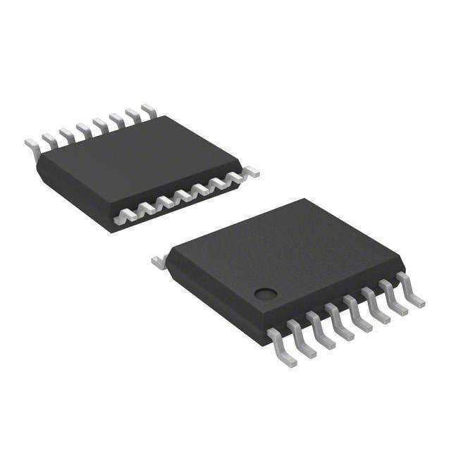
| 描述 | IC BUFF/DVR TRI-ST HEX 16TSSOP缓冲器和线路驱动器 Hex Buff & Line Drv w/3-State Outputs |
| 产品分类 | |
| 品牌 | Texas Instruments |
| 产品手册 | http://www.ti.com/litv/scls398g |
| 产品图片 |
|
| rohs | 符合RoHS无铅 / 符合限制有害物质指令(RoHS)规范要求 |
| 产品系列 | 逻辑集成电路,缓冲器和线路驱动器,Texas Instruments SN74LV367APWT74LV |
| 数据手册 | |
| 产品型号 | SN74LV367APWT |
| 产品种类 | Logic - Buffers, Drivers, and Transceivers |
| 传播延迟时间 | 17.5 ns at 2.5 V, 11.8 ns at 3.3, 7.9 ns at 5 V |
| 低电平输出电流 | 16 mA |
| 供应商器件封装 | 16-TSSOP |
| 元件数 | 2 |
| 其它名称 | 296-31875-6 |
| 包装 | Digi-Reel® |
| 单位重量 | 62 mg |
| 商标 | Texas Instruments |
| 安装类型 | 表面贴装 |
| 安装风格 | SMD/SMT |
| 封装 | Reel |
| 封装/外壳 | 16-TSSOP(0.173",4.40mm 宽) |
| 封装/箱体 | TSSOP-16 |
| 工作温度 | -40°C ~ 85°C |
| 工厂包装数量 | 250 |
| 最大工作温度 | + 85 C |
| 最小工作温度 | - 40 C |
| 极性 | Non-Inverting |
| 标准包装 | 1 |
| 每元件位数 | 2,4(六路) |
| 每芯片的通道数量 | 5 |
| 电压-电源 | 2 V ~ 5.5 V |
| 电流-输出高,低 | 16mA,16mA |
| 电源电压-最大 | 5.5 V |
| 电源电压-最小 | 2 V |
| 电源电流 | 0.02 mA |
| 系列 | SN74LV367A |
| 输入线路数量 | 6 |
| 输出类型 | 3-State |
| 输出线路数量 | 6 |
| 逻辑类型 | 缓冲器/线路驱动器,非反相 |
| 逻辑系列 | LV |
| 高电平输出电流 | - 16 mA |


- 商务部:美国ITC正式对集成电路等产品启动337调查
- 曝三星4nm工艺存在良率问题 高通将骁龙8 Gen1或转产台积电
- 太阳诱电将投资9.5亿元在常州建新厂生产MLCC 预计2023年完工
- 英特尔发布欧洲新工厂建设计划 深化IDM 2.0 战略
- 台积电先进制程称霸业界 有大客户加持明年业绩稳了
- 达到5530亿美元!SIA预计今年全球半导体销售额将创下新高
- 英特尔拟将自动驾驶子公司Mobileye上市 估值或超500亿美元
- 三星加码芯片和SET,合并消费电子和移动部门,撤换高东真等 CEO
- 三星电子宣布重大人事变动 还合并消费电子和移动部门
- 海关总署:前11个月进口集成电路产品价值2.52万亿元 增长14.8%


PDF Datasheet 数据手册内容提取
(cid:1)(cid:2)(cid:3)(cid:4)(cid:5)(cid:6)(cid:7)(cid:8)(cid:9)(cid:10)(cid:11) (cid:1)(cid:2)(cid:9)(cid:4)(cid:5)(cid:6)(cid:7)(cid:8)(cid:9)(cid:10) (cid:12)(cid:13)(cid:14) (cid:15)(cid:16)(cid:17)(cid:17)(cid:13)(cid:18)(cid:1) (cid:10)(cid:2)(cid:19) (cid:5)(cid:20)(cid:2)(cid:13) (cid:19)(cid:18)(cid:20)(cid:6)(cid:13)(cid:18)(cid:1) (cid:21)(cid:20)(cid:22)(cid:12) (cid:7)(cid:23)(cid:1)(cid:22)(cid:10)(cid:22)(cid:13) (cid:24)(cid:16)(cid:22)(cid:25)(cid:16)(cid:22)(cid:1) SCLS398G − APRIL 1998 − REVISED APRIL 2005 (cid:1) 2-V to 5.5-V V Operation SN54LV367A...J OR W PACKAGE CC (cid:1) SN74LV367A...D, DB, DGV, NS, OR PW PACKAGE Max tpd of 7 ns at 5 V (TOP VIEW) (cid:1) Typical V (Output Ground Bounce) OLP <0.8 V at VCC = 3.3 V, TA = 25°C 1OE 1 16 VCC (cid:1) Typical V (Output V Undershoot) 1A1 2 15 2OE OHV OH >2.3 V at V = 3.3 V, T = 25°C 1Y1 3 14 2A2 CC A (cid:1) 1A2 4 13 2Y2 Support Mixed-Mode Voltage Operation on 1Y2 5 12 2A1 All Ports (cid:1) 1A3 6 11 2Y1 Latch-Up Performance Exceeds 100 mA Per 1Y3 7 10 1A4 JESD 78, Class II GND 8 9 1Y4 (cid:1) ESD Protection Exceeds JESD 22 − 2000-V Human-Body Model (A114-A) SN54LV367A...FK PACKAGE − 200-V Machine Model (A115-A) (TOP VIEW) − 1000-V Charged-Device Model (C101) 1 E CE A O C CO description/ordering information 1 1 N V 2 3 2 1 20 19 The ’LV367A devices are hex buffers and line 1Y1 4 18 2A2 drivers designed for 2-V to 5.5-V VCC operation. 1A2 5 17 2Y2 These devices are designed specifically to NC 6 16 NC improve both the performance and density of 1Y2 7 15 2A1 3-state memory address drivers, clock drivers, 1A3 8 14 2Y1 and bus-oriented receivers and transmitters. 9 10 1112 13 The ’LV367A devices are organized as dual 4-line Y3ND NCY4 A4 and 2-line buffers/drivers with active-low 1G 1 1 output-enable (1OE and 2OE) inputs. When OE is NC − No internal connection low, the device passes noninverted data from the A inputs to the Y outputs. When OE is high, the outputs are in the high-impedance state. To ensure the high-impedance state during power up or power down, OE should be tied to VCC through a pullup resistor; the minimum value of the resistor is determined by the current-sinking capability of the driver. ORDERING INFORMATION ORDERABLE TOP-SIDE TA PACKAGE† PART NUMBER MARKING Tube of 40 SN74LV367AD SSOOIICC −− DD LLVV336677AA Reel of 2500 SN74LV367ADR SOP − NS Reel of 2000 SN74LV367ANSR 74LV367A −−4400°CC ttoo 8855°CC SSOP − DB Reel of 2000 SN74LV367ADBR LV36A Reel of 2000 SN74LV367APWR TTSSSSOOPP −− PPWW LLVV336677AA Reel of 250 SN74LV367APWT TVSOP − DGV Reel of 2000 SN74LV367ADGVR LV367A CDIP − J Tube of 25 SNJ54LV367AJ SNJ54LV367AJ −−5555°CC ttoo 112255°CC CFP − W Tube of 150 SNJ54LV367AW SNJ54LV367AW LCCC − FK Tube of 55 SNJ54LV367AFK SNJ54LV367AFK †Package drawings, standard packing quantities, thermal data, symbolization, and PCB design guidelines are available at www.ti.com/sc/package. Please be aware that an important notice concerning availability, standard warranty, and use in critical applications of TexasInstruments semiconductor products and disclaimers thereto appears at the end of this data sheet. (cid:16)(cid:2)(cid:5)(cid:13)(cid:1)(cid:1) (cid:24)(cid:22)(cid:12)(cid:13)(cid:18)(cid:21)(cid:20)(cid:1)(cid:13) (cid:2)(cid:24)(cid:22)(cid:13)(cid:19) (cid:26)(cid:27)(cid:28)(cid:29) (cid:30)(cid:31)!"#$%(cid:26) !(cid:31)%(cid:26)&(cid:28)%(cid:29) (cid:25)(cid:18)(cid:24)(cid:19)(cid:16)’(cid:22)(cid:20)(cid:24)(cid:2) Copyright 2005, Texas Instruments Incorporated (cid:19)(cid:10)(cid:22)(cid:10) (cid:28)%((cid:31))#&(cid:26)(cid:28)(cid:31)% !"))$%(cid:26) &(cid:29) (cid:31)( *"+,(cid:28)!&(cid:26)(cid:28)(cid:31)% (cid:30)&(cid:26)$- (cid:25))(cid:31)(cid:30)"!(cid:26)(cid:29) !(cid:31)%((cid:31))# (cid:26)(cid:31) (cid:29)*$!(cid:28)((cid:28)!&(cid:26)(cid:28)(cid:31)%(cid:29) *$) (cid:26)(cid:27)$ (cid:26)$)#(cid:29) (cid:31)( (cid:22)$.&(cid:29) (cid:20)%(cid:29)(cid:26))"#$%(cid:26)(cid:29) (cid:29)(cid:26)&%(cid:30)&)(cid:30) /&))&%(cid:26)0- (cid:25))(cid:31)(cid:30)"!(cid:26)(cid:28)(cid:31)% *)(cid:31)!$(cid:29)(cid:29)(cid:28)%1 (cid:30)(cid:31)$(cid:29) %(cid:31)(cid:26) %$!$(cid:29)(cid:29)&)(cid:28),0 (cid:28)%!,"(cid:30)$ (cid:26)$(cid:29)(cid:26)(cid:28)%1 (cid:31)( &,, *&)&#$(cid:26)$)(cid:29)- POST OFFICE BOX 655303 • DALLAS, TEXAS 75265 1
(cid:1)(cid:2)(cid:3)(cid:4)(cid:5)(cid:6)(cid:7)(cid:8)(cid:9)(cid:10)(cid:11) (cid:1)(cid:2)(cid:9)(cid:4)(cid:5)(cid:6)(cid:7)(cid:8)(cid:9)(cid:10) (cid:12)(cid:13)(cid:14) (cid:15)(cid:16)(cid:17)(cid:17)(cid:13)(cid:18)(cid:1) (cid:10)(cid:2)(cid:19) (cid:5)(cid:20)(cid:2)(cid:13) (cid:19)(cid:18)(cid:20)(cid:6)(cid:13)(cid:18)(cid:1) (cid:21)(cid:20)(cid:22)(cid:12) (cid:7)(cid:23)(cid:1)(cid:22)(cid:10)(cid:22)(cid:13) (cid:24)(cid:16)(cid:22)(cid:25)(cid:16)(cid:22)(cid:1) SCLS398G − APRIL 1998 − REVISED APRIL 2005 FUNCTION TABLE (each buffer/driver) INPUTS OOUUTTPPUUTT OE A Y L H H L L L H X Z logic diagram (positive logic) 1 15 1OE 2OE 2 3 12 11 1A1 1Y1 2A1 2Y1 To Three Other Channels To One Other Channel Pin numbers shown are for the D, DB, DGV, J, NS, PW, and W packages. absolute maximum ratings over operating free-air temperature range (unless otherwise noted)† Supply voltage range, V . . . . . . . . . . . . . . . . . . . . . . . . . . . . . . . . . . . . . . . . . . . . . . . . . . . . . . . . . . −0.5 V to 7 V CC Input voltage range, V (see Note 1) . . . . . . . . . . . . . . . . . . . . . . . . . . . . . . . . . . . . . . . . . . . . . . . . . . −0.5 V to 7 V I Voltage range applied to any output in the high-impedance or power-off state, VO (see Note 1) . . . . . . . . . . . . . . . . . . . . . . . . . . . . . . . . . . . . . . . . . . . . . . . . . . . −0.5 V to 7 V Output voltage range applied in the high or low state, V (see Notes 1 and 2) . . . . . . −0.5 V to V + 0.5 V O CC Input clamp current, I (V < 0) . . . . . . . . . . . . . . . . . . . . . . . . . . . . . . . . . . . . . . . . . . . . . . . . . . . . . . . . . . . −20 mA IK I Output clamp current, I (V < 0) . . . . . . . . . . . . . . . . . . . . . . . . . . . . . . . . . . . . . . . . . . . . . . . . . . . . . . . . −50 mA OK O Continuous output current, I (V = 0 to V ) . . . . . . . . . . . . . . . . . . . . . . . . . . . . . . . . . . . . . . . . . . . . . . ±35 mA O O CC Continuous current through V or GND . . . . . . . . . . . . . . . . . . . . . . . . . . . . . . . . . . . . . . . . . . . . . . . . . . . ±70 mA CC Package thermal impedance, θ (see Note 3): D package . . . . . . . . . . . . . . . . . . . . . . . . . . . . . . . . . . . 73°C/W JA DB package . . . . . . . . . . . . . . . . . . . . . . . . . . . . . . . . . 82°C/W DGV package . . . . . . . . . . . . . . . . . . . . . . . . . . . . . . . 120°C/W NS package . . . . . . . . . . . . . . . . . . . . . . . . . . . . . . . . . 64°C/W PW package . . . . . . . . . . . . . . . . . . . . . . . . . . . . . . . . 108°C/W Storage temperature range, T . . . . . . . . . . . . . . . . . . . . . . . . . . . . . . . . . . . . . . . . . . . . . . . . . . . −65°C to 150°C stg †Stresses beyond those listed under “absolute maximum ratings” may cause permanent damage to the device. These are stress ratings only, and functional operation of the device at these or any other conditions beyond those indicated under “recommended operating conditions” is not implied. Exposure to absolute-maximum-rated conditions for extended periods may affect device reliability. NOTES: 1. The input and output negative-voltage ratings may be exceeded if the input and output current ratings are observed. 2. This value is limited to 5.5 V maximum. 3. The package thermal impedance is calculated in accordance with JESD 51-7. 2 POST OFFICE BOX 655303 • DALLAS, TEXAS 75265
(cid:1)(cid:2)(cid:3)(cid:4)(cid:5)(cid:6)(cid:7)(cid:8)(cid:9)(cid:10)(cid:11) (cid:1)(cid:2)(cid:9)(cid:4)(cid:5)(cid:6)(cid:7)(cid:8)(cid:9)(cid:10) (cid:12)(cid:13)(cid:14) (cid:15)(cid:16)(cid:17)(cid:17)(cid:13)(cid:18)(cid:1) (cid:10)(cid:2)(cid:19) (cid:5)(cid:20)(cid:2)(cid:13) (cid:19)(cid:18)(cid:20)(cid:6)(cid:13)(cid:18)(cid:1) (cid:21)(cid:20)(cid:22)(cid:12) (cid:7)(cid:23)(cid:1)(cid:22)(cid:10)(cid:22)(cid:13) (cid:24)(cid:16)(cid:22)(cid:25)(cid:16)(cid:22)(cid:1) SCLS398G − APRIL 1998 − REVISED APRIL 2005 recommended operating conditions (see Note 4) SN54LV367A SN74LV367A UUNNIITT MIN MAX MIN MAX VCC Supply voltage 2 5.5 2 5.5 V VCC = 2 V 1.5 1.5 VCC = 2.3 V to 2.7 V VCC×0.7 VCC×0.7 VVIIHH HHiigghh--lleevveell iinnppuutt vvoollttaaggee VCC = 3 V to 3.6 V VCC×0.7 VCC×0.7 VV VCC = 4.5 V to 5.5 V VCC×0.7 VCC×0.7 VCC = 2 V 0.5 0.5 VCC = 2.3 V to 2.7 V VCC×0.3 VCC×0.3 VVIILL LLooww--lleevveell iinnppuutt vvoollttaaggee VCC = 3 V to 3.6 V VCC×0.3 VCC×0.3 VV VCC = 4.5 V to 5.5 V VCC×0.3 VCC×0.3 VI Input voltage 0 5.5 0 5.5 V High or low state 0 VCC 0 VCC VVOO OOuuttppuutt vvoollttaaggee VV 3-state 0 5.5 0 5.5 VCC = 2 V −50 −50 µA VCC = 2.3 V to 2.7 V −2 −2 IIOOHH HHiigghh--lleevveell oouuttppuutt ccuurrrreenntt VCC = 3 V to 3.6 V −8 −8 mmAA VCC = 4.5 V to 5.5 V −16 −16 VCC = 2 V 50 50 µA VCC = 2.3 V to 2.7 V 2 2 IIOOLL LLooww--lleevveell oouuttppuutt ccuurrrreenntt VCC = 3 V to 3.6 V 8 8 mmAA VCC = 4.5 V to 5.5 V 16 16 VCC = 2.3 V to 2.7 V 200 200 ∆∆tt//∆∆vv IInnppuutt ttrraannssiittiioonn rriissee oorr ffaallll rraattee VCC = 3 V to 3.6 V 100 100 nnss//VV VCC = 4.5 V to 5.5 V 20 20 TA Operating free-air temperature −55 125 −40 85 °C NOTE 4: All unused inputs of the device must be held at VCC or GND to ensure proper device operation. Refer to the TI application report, Implications of Slow or Floating CMOS Inputs, literature number SCBA004. (cid:25)(cid:18)(cid:24)(cid:19)(cid:16)’(cid:22) (cid:25)(cid:18)(cid:13)(cid:6)(cid:20)(cid:13)(cid:21) (cid:28)%((cid:31))#&(cid:26)(cid:28)(cid:31)% !(cid:31)%!$)%(cid:29) *)(cid:31)(cid:30)"!(cid:26)(cid:29) (cid:28)% (cid:26)(cid:27)$ ((cid:31))#&(cid:26)(cid:28)2$ (cid:31)) (cid:30)$(cid:29)(cid:28)1% *(cid:27)&(cid:29)$ (cid:31)( (cid:30)$2$,(cid:31)*#$%(cid:26)- ’(cid:27)&)&!(cid:26)$)(cid:28)(cid:29)(cid:26)(cid:28)! (cid:30)&(cid:26)& &%(cid:30) (cid:31)(cid:26)(cid:27)$) (cid:29)*$!(cid:28)((cid:28)!&(cid:26)(cid:28)(cid:31)%(cid:29) &)$ (cid:30)$(cid:29)(cid:28)1% 1(cid:31)&,(cid:29)- (cid:22)$.&(cid:29) (cid:20)%(cid:29)(cid:26))"#$%(cid:26)(cid:29) )$(cid:29)$)2$(cid:29) (cid:26)(cid:27)$ )(cid:28)1(cid:27)(cid:26) (cid:26)(cid:31) !(cid:27)&%1$ (cid:31)) (cid:30)(cid:28)(cid:29)!(cid:31)%(cid:26)(cid:28)%"$ (cid:26)(cid:27)$(cid:29)$ *)(cid:31)(cid:30)"!(cid:26)(cid:29) /(cid:28)(cid:26)(cid:27)(cid:31)"(cid:26) %(cid:31)(cid:26)(cid:28)!$- POST OFFICE BOX 655303 • DALLAS, TEXAS 75265 3
(cid:1)(cid:2)(cid:3)(cid:4)(cid:5)(cid:6)(cid:7)(cid:8)(cid:9)(cid:10)(cid:11) (cid:1)(cid:2)(cid:9)(cid:4)(cid:5)(cid:6)(cid:7)(cid:8)(cid:9)(cid:10) (cid:12)(cid:13)(cid:14) (cid:15)(cid:16)(cid:17)(cid:17)(cid:13)(cid:18)(cid:1) (cid:10)(cid:2)(cid:19) (cid:5)(cid:20)(cid:2)(cid:13) (cid:19)(cid:18)(cid:20)(cid:6)(cid:13)(cid:18)(cid:1) (cid:21)(cid:20)(cid:22)(cid:12) (cid:7)(cid:23)(cid:1)(cid:22)(cid:10)(cid:22)(cid:13) (cid:24)(cid:16)(cid:22)(cid:25)(cid:16)(cid:22)(cid:1) SCLS398G − APRIL 1998 − REVISED APRIL 2005 electrical characteristics over recommended operating free-air temperature range (unless otherwise noted) SN54LV367A SN74LV367A PPAARRAAMMEETTEERR TTEESSTT CCOONNDDIITTIIOONNSS VVCCCC UUNNIITT MIN TYP MAX MIN TYP MAX IOH = −50 µA 2 V to 5.5 V VCC−0.1 VCC−0.1 IOH = −2 mA 2.3 V 2 2 VVOOHH VV IOH = −8 mA 3 V 2.48 2.48 IOH = −16 mA 4.5 V 3.8 3.8 IOL = 50 µA 2 V to 5.5 V 0.1 0.1 IOL = 2 mA 2.3 V 0.4 0.4 VVOOLL VV IOL = 8 mA 3 V 0.44 0.44 IOL = 16 mA 4.5 V 0.55 0.55 II VI = 5.5 V or GND 0 to 5.5 V ±1 ±1 µA IOZ VO = VCC or GND 5.5 V ±5 ±5 µA ICC VI = VCC or GND, IO = 0 5.5 V 20 20 µA Ioff VI or VO = 0 to 5.5 V 0 5 5 µA Ci VI = VCC or GND 3.3 V 3 3 pF Co VI = VCC or GND 3.3 V 5.2 5.2 pF switching characteristics over recommended operating free-air temperature range, V = 2.5 V ± 0.2 V (unless otherwise noted) (see Figure 1) CC FFRROOMM TTOO LLOOAADD TA = 25°C SN54LV367A SN74LV367A PPAARRAAMMEETTEERR UUNNIITT (INPUT) (OUTPUT) CAPACITANCE MIN TYP MAX MIN MAX MIN MAX tpd A Y 6.4* 12.7* 1* 16* 1 16 ten OE Y CCLL == 1155 ppFF 6.9* 14.9* 1* 20* 1 20 nnss tdis OE Y 6.4* 14.9* 1* 20* 1 20 tpd A Y 8.6 17.5 1 21 1 21 ten OE Y 9.4 19.7 1 25 1 25 CCLL == 5500 ppFF nnss tdis OE Y 10.1 19.7 1 25 1 25 tsk(o) 2 2 * On products compliant to MIL-PRF-38535, this parameter is not production tested. switching characteristics over recommended operating free-air temperature range, V = 3.3 V ± 0.3 V (unless otherwise noted) (see Figure 1) CC FFRROOMM TTOO LLOOAADD TA = 25°C SN54LV367A SN74LV367A PPAARRAAMMEETTEERR UUNNIITT (INPUT) (OUTPUT) CAPACITANCE MIN TYP MAX MIN MAX MIN MAX tpd A Y 4.7* 8.3* 1* 10* 1 10 ten OE Y CCLL == 1155 ppFF 5.1* 10.5* 1* 12.5* 1 12.5 nnss tdis OE Y 4.9* 10.5* 1* 12.5* 1 12.5 tpd A Y 6.2 11.8 1 13.5 1 13.5 ten OE Y 6.8 14 1 16 1 16 CCLL == 5500 ppFF nnss tdis OE Y 7.3 13.6 1 15.5 1 15.5 tsk(o) 1.5 1.5 * On products compliant to MIL-PRF-38535, this parameter is not production tested. (cid:25)(cid:18)(cid:24)(cid:19)(cid:16)’(cid:22) (cid:25)(cid:18)(cid:13)(cid:6)(cid:20)(cid:13)(cid:21) (cid:28)%((cid:31))#&(cid:26)(cid:28)(cid:31)% !(cid:31)%!$)%(cid:29) *)(cid:31)(cid:30)"!(cid:26)(cid:29) (cid:28)% (cid:26)(cid:27)$ ((cid:31))#&(cid:26)(cid:28)2$ (cid:31)) (cid:30)$(cid:29)(cid:28)1% *(cid:27)&(cid:29)$ (cid:31)( (cid:30)$2$,(cid:31)*#$%(cid:26)- ’(cid:27)&)&!(cid:26)$)(cid:28)(cid:29)(cid:26)(cid:28)! (cid:30)&(cid:26)& &%(cid:30) (cid:31)(cid:26)(cid:27)$) (cid:29)*$!(cid:28)((cid:28)!&(cid:26)(cid:28)(cid:31)%(cid:29) &)$ (cid:30)$(cid:29)(cid:28)1% 1(cid:31)&,(cid:29)- (cid:22)$.&(cid:29) (cid:20)%(cid:29)(cid:26))"#$%(cid:26)(cid:29) )$(cid:29)$)2$(cid:29) (cid:26)(cid:27)$ )(cid:28)1(cid:27)(cid:26) (cid:26)(cid:31) !(cid:27)&%1$ (cid:31)) (cid:30)(cid:28)(cid:29)!(cid:31)%(cid:26)(cid:28)%"$ (cid:26)(cid:27)$(cid:29)$ *)(cid:31)(cid:30)"!(cid:26)(cid:29) /(cid:28)(cid:26)(cid:27)(cid:31)"(cid:26) %(cid:31)(cid:26)(cid:28)!$- 4 POST OFFICE BOX 655303 • DALLAS, TEXAS 75265
(cid:1)(cid:2)(cid:3)(cid:4)(cid:5)(cid:6)(cid:7)(cid:8)(cid:9)(cid:10)(cid:11) (cid:1)(cid:2)(cid:9)(cid:4)(cid:5)(cid:6)(cid:7)(cid:8)(cid:9)(cid:10) (cid:12)(cid:13)(cid:14) (cid:15)(cid:16)(cid:17)(cid:17)(cid:13)(cid:18)(cid:1) (cid:10)(cid:2)(cid:19) (cid:5)(cid:20)(cid:2)(cid:13) (cid:19)(cid:18)(cid:20)(cid:6)(cid:13)(cid:18)(cid:1) (cid:21)(cid:20)(cid:22)(cid:12) (cid:7)(cid:23)(cid:1)(cid:22)(cid:10)(cid:22)(cid:13) (cid:24)(cid:16)(cid:22)(cid:25)(cid:16)(cid:22)(cid:1) SCLS398G − APRIL 1998 − REVISED APRIL 2005 switching characteristics over recommended operating free-air temperature range, V = 5 V ± 0.5 V (unless otherwise noted) (see Figure 1) CC FFRROOMM TTOO LLOOAADD TA = 25°C SN54LV367A SN74LV367A PPAARRAAMMEETTEERR UUNNIITT (INPUT) (OUTPUT) CAPACITANCE MIN TYP MAX MIN MAX MIN MAX tpd A Y 3.6* 5.9* 1* 7* 1 7 ten OE Y CCLL == 1155 ppFF 3.8* 7.2* 1* 8.5* 1 8.5 nnss tdis OE Y 2.6* 7.2* 1* 8.5* 0 8.5 tpd A Y 4.5 7.9 1 9 1 9 ten OE Y 4.9 9.2 1 10.5 1 10.5 CCLL == 5500 ppFF nnss tdis OE Y 4.5 9.2 1 10.5 0 10.5 tsk(o) 1 1 * On products compliant to MIL-PRF-38535, this parameter is not production tested. noise characteristics, VCC = 3.3 V, CL = 50 pF, TA = 25°C (see Note 5) SN74LV367A PPAARRAAMMEETTEERR UUNNIITT MIN TYP MAX VOL(P) Quiet output, maximum dynamic VOL 0.5 0.8 V VOL(V) Quiet output, minimum dynamic VOL −0.2 −0.8 V VOH(V) Quiet output, minimum dynamic VOH 3 V VIH(D) High-level dynamic input voltage 2.31 V VIL(D) Low-level dynamic input voltage 0.99 V NOTE 5: Characteristics are for surface-mount packages only. operating characteristics, T = 25°C A PARAMETER TEST CONDITIONS VCC TYP UNIT 3.3 V 14.9 CCppdd PPoowweerr ddiissssiippaattiioonn ccaappaacciittaannccee CCLL == 5500 ppFF,, ff == 1100 MMHHzz ppFF 5 V 17.4 (cid:25)(cid:18)(cid:24)(cid:19)(cid:16)’(cid:22) (cid:25)(cid:18)(cid:13)(cid:6)(cid:20)(cid:13)(cid:21) (cid:28)%((cid:31))#&(cid:26)(cid:28)(cid:31)% !(cid:31)%!$)%(cid:29) *)(cid:31)(cid:30)"!(cid:26)(cid:29) (cid:28)% (cid:26)(cid:27)$ ((cid:31))#&(cid:26)(cid:28)2$ (cid:31)) (cid:30)$(cid:29)(cid:28)1% *(cid:27)&(cid:29)$ (cid:31)( (cid:30)$2$,(cid:31)*#$%(cid:26)- ’(cid:27)&)&!(cid:26)$)(cid:28)(cid:29)(cid:26)(cid:28)! (cid:30)&(cid:26)& &%(cid:30) (cid:31)(cid:26)(cid:27)$) (cid:29)*$!(cid:28)((cid:28)!&(cid:26)(cid:28)(cid:31)%(cid:29) &)$ (cid:30)$(cid:29)(cid:28)1% 1(cid:31)&,(cid:29)- (cid:22)$.&(cid:29) (cid:20)%(cid:29)(cid:26))"#$%(cid:26)(cid:29) )$(cid:29)$)2$(cid:29) (cid:26)(cid:27)$ )(cid:28)1(cid:27)(cid:26) (cid:26)(cid:31) !(cid:27)&%1$ (cid:31)) (cid:30)(cid:28)(cid:29)!(cid:31)%(cid:26)(cid:28)%"$ (cid:26)(cid:27)$(cid:29)$ *)(cid:31)(cid:30)"!(cid:26)(cid:29) /(cid:28)(cid:26)(cid:27)(cid:31)"(cid:26) %(cid:31)(cid:26)(cid:28)!$- POST OFFICE BOX 655303 • DALLAS, TEXAS 75265 5
(cid:1)(cid:2)(cid:3)(cid:4)(cid:5)(cid:6)(cid:7)(cid:8)(cid:9)(cid:10)(cid:11) (cid:1)(cid:2)(cid:9)(cid:4)(cid:5)(cid:6)(cid:7)(cid:8)(cid:9)(cid:10) (cid:12)(cid:13)(cid:14) (cid:15)(cid:16)(cid:17)(cid:17)(cid:13)(cid:18)(cid:1) (cid:10)(cid:2)(cid:19) (cid:5)(cid:20)(cid:2)(cid:13) (cid:19)(cid:18)(cid:20)(cid:6)(cid:13)(cid:18)(cid:1) (cid:21)(cid:20)(cid:22)(cid:12) (cid:7)(cid:23)(cid:1)(cid:22)(cid:10)(cid:22)(cid:13) (cid:24)(cid:16)(cid:22)(cid:25)(cid:16)(cid:22)(cid:1) SCLS398G − APRIL 1998 − REVISED APRIL 2005 PARAMETER MEASUREMENT INFORMATION VCC From Output Test From Output RL = 1 kΩ S1 Open TEST S1 Under Test Point Under Test GND tPLH/tPHL Open CL CL tPLZ/tPZL VCC (see Note A) (see Note A) tPHZ/tPZH GND Open Drain VCC LOAD CIRCUIT FOR LOAD CIRCUIT FOR TOTEM-POLE OUTPUTS 3-STATE AND OPEN-DRAIN OUTPUTS VCC Timing Input 50% VCC tw th 0 V VCC tsu VCC Input 50% VCC 50% VCC Data Input 50% VCC 50% VCC 0 V 0 V VOLTAGE WAVEFORMS VOLTAGE WAVEFORMS PULSE DURATION SETUP AND HOLD TIMES VCC VCC Output Input 50% VCC 50% VCC Control 50% VCC 50% VCC 0 V 0 V tPLH tPHL tPZL tPLZ Output In-Phase VOH Waveform 1 ≈VCC Output 50% VCC 50% VCC S1 at VCC 50% VCC VOL + 0.3 V VOL (see Note B) VOL tPHL tPLH tPZH tPHZ Output Out-ofO-Puhtapsuet 50% VCC 50% VCVCOH WSa1v eafto GrmN D2 50% VCC VOH − 0.3 VVOH VOL (see Note B) ≈0 V VOLTAGE WAVEFORMS VOLTAGE WAVEFORMS PROPAGATION DELAY TIMES ENABLE AND DISABLE TIMES INVERTING AND NONINVERTING OUTPUTS LOW- AND HIGH-LEVEL ENABLING NOTES: A. CL includes probe and jig capacitance. B. Waveform 1 is for an output with internal conditions such that the output is low, except when disabled by the output control. Waveform 2 is for an output with internal conditions such that the output is high, except when disabled by the output control. C. All input pulses are supplied by generators having the following characteristics: PRR ≤ 1 MHz, ZO = 50 Ω, tr ≤3 ns, tf ≤ 3 ns. D. The outputs are measured one at a time, with one input transition per measurement. E. tPLZ and tPHZ are the same as tdis. F. tPZL and tPZH are the same as ten. G. tPHL and tPLH are the same as tpd. H. All parameters and waveforms are not applicable to all devices. Figure 1. Load Circuit and Voltage Waveforms 6 POST OFFICE BOX 655303 • DALLAS, TEXAS 75265
PACKAGE OPTION ADDENDUM www.ti.com 15-Apr-2017 PACKAGING INFORMATION Orderable Device Status Package Type Package Pins Package Eco Plan Lead/Ball Finish MSL Peak Temp Op Temp (°C) Device Marking Samples (1) Drawing Qty (2) (6) (3) (4/5) SN74LV367AD ACTIVE SOIC D 16 40 Green (RoHS CU NIPDAU Level-1-260C-UNLIM -40 to 85 LV367A & no Sb/Br) SN74LV367ADE4 ACTIVE SOIC D 16 40 Green (RoHS CU NIPDAU Level-1-260C-UNLIM -40 to 85 LV367A & no Sb/Br) SN74LV367ADGVR ACTIVE TVSOP DGV 16 2000 Green (RoHS CU NIPDAU Level-1-260C-UNLIM -40 to 85 LV367A & no Sb/Br) SN74LV367ADR ACTIVE SOIC D 16 2500 Green (RoHS CU NIPDAU Level-1-260C-UNLIM -40 to 85 LV367A & no Sb/Br) SN74LV367ANSR ACTIVE SO NS 16 2000 Green (RoHS CU NIPDAU Level-1-260C-UNLIM -40 to 85 74LV367A & no Sb/Br) SN74LV367APWR ACTIVE TSSOP PW 16 2000 Green (RoHS CU NIPDAU Level-1-260C-UNLIM -40 to 85 LV367A & no Sb/Br) SN74LV367APWRG4 ACTIVE TSSOP PW 16 2000 Green (RoHS CU NIPDAU Level-1-260C-UNLIM -40 to 85 LV367A & no Sb/Br) SN74LV367APWT ACTIVE TSSOP PW 16 250 Green (RoHS CU NIPDAU Level-1-260C-UNLIM -40 to 85 LV367A & no Sb/Br) (1) The marketing status values are defined as follows: ACTIVE: Product device recommended for new designs. LIFEBUY: TI has announced that the device will be discontinued, and a lifetime-buy period is in effect. NRND: Not recommended for new designs. Device is in production to support existing customers, but TI does not recommend using this part in a new design. PREVIEW: Device has been announced but is not in production. Samples may or may not be available. OBSOLETE: TI has discontinued the production of the device. (2) Eco Plan - The planned eco-friendly classification: Pb-Free (RoHS), Pb-Free (RoHS Exempt), or Green (RoHS & no Sb/Br) - please check http://www.ti.com/productcontent for the latest availability information and additional product content details. TBD: The Pb-Free/Green conversion plan has not been defined. Pb-Free (RoHS): TI's terms "Lead-Free" or "Pb-Free" mean semiconductor products that are compatible with the current RoHS requirements for all 6 substances, including the requirement that lead not exceed 0.1% by weight in homogeneous materials. Where designed to be soldered at high temperatures, TI Pb-Free products are suitable for use in specified lead-free processes. Pb-Free (RoHS Exempt): This component has a RoHS exemption for either 1) lead-based flip-chip solder bumps used between the die and package, or 2) lead-based die adhesive used between the die and leadframe. The component is otherwise considered Pb-Free (RoHS compatible) as defined above. Green (RoHS & no Sb/Br): TI defines "Green" to mean Pb-Free (RoHS compatible), and free of Bromine (Br) and Antimony (Sb) based flame retardants (Br or Sb do not exceed 0.1% by weight in homogeneous material) (3) MSL, Peak Temp. - The Moisture Sensitivity Level rating according to the JEDEC industry standard classifications, and peak solder temperature. Addendum-Page 1
PACKAGE OPTION ADDENDUM www.ti.com 15-Apr-2017 (4) There may be additional marking, which relates to the logo, the lot trace code information, or the environmental category on the device. (5) Multiple Device Markings will be inside parentheses. Only one Device Marking contained in parentheses and separated by a "~" will appear on a device. If a line is indented then it is a continuation of the previous line and the two combined represent the entire Device Marking for that device. (6) Lead/Ball Finish - Orderable Devices may have multiple material finish options. Finish options are separated by a vertical ruled line. Lead/Ball Finish values may wrap to two lines if the finish value exceeds the maximum column width. Important Information and Disclaimer:The information provided on this page represents TI's knowledge and belief as of the date that it is provided. TI bases its knowledge and belief on information provided by third parties, and makes no representation or warranty as to the accuracy of such information. Efforts are underway to better integrate information from third parties. TI has taken and continues to take reasonable steps to provide representative and accurate information but may not have conducted destructive testing or chemical analysis on incoming materials and chemicals. TI and TI suppliers consider certain information to be proprietary, and thus CAS numbers and other limited information may not be available for release. In no event shall TI's liability arising out of such information exceed the total purchase price of the TI part(s) at issue in this document sold by TI to Customer on an annual basis. Addendum-Page 2
PACKAGE MATERIALS INFORMATION www.ti.com 10-Aug-2016 TAPE AND REEL INFORMATION *Alldimensionsarenominal Device Package Package Pins SPQ Reel Reel A0 B0 K0 P1 W Pin1 Type Drawing Diameter Width (mm) (mm) (mm) (mm) (mm) Quadrant (mm) W1(mm) SN74LV367ADGVR TVSOP DGV 16 2000 330.0 12.4 6.8 4.0 1.6 8.0 12.0 Q1 SN74LV367ADR SOIC D 16 2500 330.0 16.4 6.5 10.3 2.1 8.0 16.0 Q1 SN74LV367ANSR SO NS 16 2000 330.0 16.4 8.2 10.5 2.5 12.0 16.0 Q1 SN74LV367APWR TSSOP PW 16 2000 330.0 12.4 6.9 5.6 1.6 8.0 12.0 Q1 SN74LV367APWT TSSOP PW 16 250 330.0 12.4 6.9 5.6 1.6 8.0 12.0 Q1 PackMaterials-Page1
PACKAGE MATERIALS INFORMATION www.ti.com 10-Aug-2016 *Alldimensionsarenominal Device PackageType PackageDrawing Pins SPQ Length(mm) Width(mm) Height(mm) SN74LV367ADGVR TVSOP DGV 16 2000 367.0 367.0 35.0 SN74LV367ADR SOIC D 16 2500 333.2 345.9 28.6 SN74LV367ANSR SO NS 16 2000 367.0 367.0 38.0 SN74LV367APWR TSSOP PW 16 2000 367.0 367.0 35.0 SN74LV367APWT TSSOP PW 16 250 367.0 367.0 35.0 PackMaterials-Page2
None
None
PACKAGE OUTLINE PW0016A TSSOP - 1.2 mm max height SCALE 2.500 SMALL OUTLINE PACKAGE SEATING PLANE C 6.6 TYP 6.2 A 0.1 C PIN 1 INDEX AREA 14X 0.65 16 1 2X 5.1 4.55 4.9 NOTE 3 8 9 0.30 B 4.5 16X 0.19 1.2 MAX 4.3 0.1 C A B NOTE 4 (0.15) TYP SEE DETAIL A 0.25 GAGE PLANE 0.15 0.05 0.75 0.50 0 -8 DETA 20AIL A TYPICAL 4220204/A 02/2017 NOTES: 1. All linear dimensions are in millimeters. Any dimensions in parenthesis are for reference only. Dimensioning and tolerancing per ASME Y14.5M. 2. This drawing is subject to change without notice. 3. This dimension does not include mold flash, protrusions, or gate burrs. Mold flash, protrusions, or gate burrs shall not exceed 0.15 mm per side. 4. This dimension does not include interlead flash. Interlead flash shall not exceed 0.25 mm per side. 5. Reference JEDEC registration MO-153. www.ti.com
EXAMPLE BOARD LAYOUT PW0016A TSSOP - 1.2 mm max height SMALL OUTLINE PACKAGE 16X (1.5) SYMM (R0.05) TYP 1 16X (0.45) 16 SYMM 14X (0.65) 8 9 (5.8) LAND PATTERN EXAMPLE EXPOSED METAL SHOWN SCALE: 10X SOLDER MASK METAL UNDER SOLDER MASK OPENING METAL SOLDER MASK OPENING EXPOSED METAL EXPOSED METAL 0.05 MAX 0.05 MIN ALL AROUND ALL AROUND NON-SOLDER MASK SOLDER MASK DEFINED DEFINED (PREFERRED) SOLDE15.000R MASK DETAILS 4220204/A 02/2017 NOTES: (continued) 6. Publication IPC-7351 may have alternate designs. 7. Solder mask tolerances between and around signal pads can vary based on board fabrication site. www.ti.com
EXAMPLE STENCIL DESIGN PW0016A TSSOP - 1.2 mm max height SMALL OUTLINE PACKAGE 16X (1.5) SYMM (R0.05) TYP 1 16X (0.45) 16 SYMM 14X (0.65) 8 9 (5.8) SOLDER PASTE EXAMPLE BASED ON 0.125 mm THICK STENCIL SCALE: 10X 4220204/A 02/2017 NOTES: (continued) 8. Laser cutting apertures with trapezoidal walls and rounded corners may offer better paste release. IPC-7525 may have alternate design recommendations. 9. Board assembly site may have different recommendations for stencil design. www.ti.com
None
MECHANICAL DATA MPDS006C – FEBRUARY 1996 – REVISED AUGUST 2000 DGV (R-PDSO-G**) PLASTIC SMALL-OUTLINE 24 PINS SHOWN 0,23 0,40 0,07 M 0,13 24 13 0,16 NOM 4,50 6,60 4,30 6,20 Gage Plane 0,25 0°–(cid:1)8° 0,75 1 12 0,50 A Seating Plane 0,15 1,20 MAX 0,08 0,05 PINS ** 14 16 20 24 38 48 56 DIM A MAX 3,70 3,70 5,10 5,10 7,90 9,80 11,40 A MIN 3,50 3,50 4,90 4,90 7,70 9,60 11,20 4073251/E 08/00 NOTES: A. All linear dimensions are in millimeters. B. This drawing is subject to change without notice. C. Body dimensions do not include mold flash or protrusion, not to exceed 0,15 per side. D. Falls within JEDEC: 24/48 Pins – MO-153 14/16/20/56 Pins – MO-194 • POST OFFICE BOX 655303 DALLAS, TEXAS 75265
IMPORTANTNOTICEANDDISCLAIMER TIPROVIDESTECHNICALANDRELIABILITYDATA(INCLUDINGDATASHEETS),DESIGNRESOURCES(INCLUDINGREFERENCE DESIGNS),APPLICATIONOROTHERDESIGNADVICE,WEBTOOLS,SAFETYINFORMATION,ANDOTHERRESOURCES“ASIS” ANDWITHALLFAULTS,ANDDISCLAIMSALLWARRANTIES,EXPRESSANDIMPLIED,INCLUDINGWITHOUTLIMITATIONANY IMPLIEDWARRANTIESOFMERCHANTABILITY,FITNESSFORAPARTICULARPURPOSEORNON-INFRINGEMENTOFTHIRD PARTYINTELLECTUALPROPERTYRIGHTS. TheseresourcesareintendedforskilleddevelopersdesigningwithTIproducts.Youaresolelyresponsiblefor(1)selectingtheappropriate TIproductsforyourapplication,(2)designing,validatingandtestingyourapplication,and(3)ensuringyourapplicationmeetsapplicable standards,andanyothersafety,security,orotherrequirements.Theseresourcesaresubjecttochangewithoutnotice.TIgrantsyou permissiontousetheseresourcesonlyfordevelopmentofanapplicationthatusestheTIproductsdescribedintheresource.Other reproductionanddisplayoftheseresourcesisprohibited.NolicenseisgrantedtoanyotherTIintellectualpropertyrightortoanythird partyintellectualpropertyright.TIdisclaimsresponsibilityfor,andyouwillfullyindemnifyTIanditsrepresentativesagainst,anyclaims, damages,costs,losses,andliabilitiesarisingoutofyouruseoftheseresources. TI’sproductsareprovidedsubjecttoTI’sTermsofSale(www.ti.com/legal/termsofsale.html)orotherapplicabletermsavailableeitheron ti.comorprovidedinconjunctionwithsuchTIproducts.TI’sprovisionoftheseresourcesdoesnotexpandorotherwisealterTI’sapplicable warrantiesorwarrantydisclaimersforTIproducts. MailingAddress:TexasInstruments,PostOfficeBox655303,Dallas,Texas75265 Copyright©2019,TexasInstrumentsIncorporated