ICGOO在线商城 > 集成电路(IC) > 逻辑 - 缓冲器,驱动器,接收器,收发器 > 74HC3G34DC,125
 Datasheet下载
- 型号: 74HC3G34DC,125
- 制造商: NXP Semiconductors
- 库位|库存: xxxx|xxxx
- 要求:
| 数量阶梯 | 香港交货 | 国内含税 |
| +xxxx | $xxxx | ¥xxxx |
查看当月历史价格
查看今年历史价格
74HC3G34DC,125产品简介:
ICGOO电子元器件商城为您提供74HC3G34DC,125由NXP Semiconductors设计生产,在icgoo商城现货销售,并且可以通过原厂、代理商等渠道进行代购。 74HC3G34DC,125价格参考。NXP Semiconductors74HC3G34DC,125封装/规格:逻辑 - 缓冲器,驱动器,接收器,收发器, Buffer, Non-Inverting 3 Element 1 Bit per Element Push-Pull Output 8-VSSOP。您可以下载74HC3G34DC,125参考资料、Datasheet数据手册功能说明书,资料中有74HC3G34DC,125 详细功能的应用电路图电压和使用方法及教程。
Nexperia USA Inc. 生产的 74HC3G34DC,125 是一款逻辑缓冲器,属于 74HC 系列的三态非门 (Three-state Inverter)。这款器件主要用于数字电路设计中,特别是在需要信号电平转换、驱动能力增强或三态控制的应用场景中。

 主要应用场景:

1. 信号调理与驱动:
   - 在数字电路中,74HC3G34DC,125 可以用于增强弱信号的驱动能力。例如,在长距离传输线路上,信号可能会因为线路阻抗而衰减,使用该器件可以确保信号在传输过程中保持足够的强度。

2. 三态控制:
   - 该器件具有三态输出功能,允许输出高阻态(High-Z)。这意味着它可以方便地与其他设备共享同一总线,而不会产生信号冲突。这种特性常用于多主设备系统中,如计算机内部的总线系统或多路复用器。

3. 电平转换:
   - 74HC3G34DC,125 工作电压范围为 2V 至 6V,适用于不同电源电压下的逻辑电平转换。例如,在混合信号系统中,某些模块可能工作在不同的电压下,该器件可以帮助实现这些模块之间的电平兼容。

4. 噪声抑制:
   - 由于其高速特性和低功耗设计,74HC3G34DC,125 可以有效减少数字信号中的噪声干扰,特别适合在高频应用中使用。例如,在通信设备或高速数据传输系统中,它可以帮助提高信号的完整性和可靠性。

5. 简化电路设计:
   - 该器件集成了多个功能,减少了外部元件的需求,从而简化了电路设计。例如,在需要多个非门和三态控制的场合,使用一个 74HC3G34DC,125 可以替代多个分立元件,节省空间并降低成本。

总之,74HC3G34DC,125 是一款多功能的逻辑缓冲器,广泛应用于各种数字电路中,尤其是在需要信号调理、三态控制和电平转换的场合。
| 参数 | 数值 |
| 产品目录 | 集成电路 (IC) |
| 描述 | IC BUFFER NON-INV TRIPLE 8VSSOP |
| 产品分类 | |
| 品牌 | NXP Semiconductors |
| 数据手册 | |
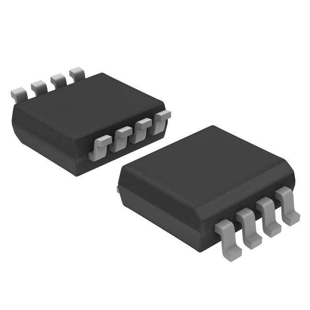
| 产品图片 |
|
| 产品型号 | 74HC3G34DC,125 |
| rohs | 无铅 / 符合限制有害物质指令(RoHS)规范要求 |
| 产品系列 | 74HC |
| 供应商器件封装 | 8-VSSOP |
| 元件数 | 3 |
| 其它名称 | 568-9239-6 |
| 包装 | Digi-Reel® |
| 安装类型 | 表面贴装 |
| 封装/外壳 | 8-VFSOP(0.091",2.30mm 宽) |
| 工作温度 | -40°C ~ 125°C |
| 标准包装 | 1 |
| 每元件位数 | 1 |
| 电压-电源 | 2 V ~ 6 V |
| 电流-输出高,低 | 5.2mA,5.2mA |
| 逻辑类型 | 缓冲器/线路驱动器,非反相 |


PDF Datasheet 数据手册内容提取
74HC3G34; 74HCT3G34 Triple buffer gate Rev. 7 — 11 June 2018 Product data sheet 1 General description The 74HC3G34; 74HCT3G34 is a triple buffer. Inputs include clamp diodes. This enables the use of current limiting resistors to interface inputs to voltages in excess of V . CC 2 Features and benefits • Wide supply voltage range from 2.0 V to 6.0 V • Input levels: –For 74HC3G34: CMOS level –For 74HCT3G34: TTL level • Complies with JEDEC standard no. 7 A • Symmetrical output impedance • High noise immunity • Low-power dissipation • Balanced propagation delays • Multiple package options • ESD protection: –HBM JESD22-A114E exceeds 2000 V –MM JESD22-A115-A exceeds 200 V • Specified from -40 °C to +85 °C and -40 °C to +125 °C 3 Ordering information Table 1. Ordering information Type number Package Temperature range Name Description Version 74HC3G34DP -40 °C to +125 °C TSSOP8 plastic thin shrink small outline package; 8 leads; SOT505-2 body width 3 mm; lead length 0.5 mm 74HCT3G34DP 74HC3G34DC -40 °C to +125 °C VSSOP8 plastic very thin shrink small outline package; SOT765-1 8 leads; body width 2.3 mm 74HCT3G34DC
Nexperia 74HC3G34; 74HCT3G34 Triple buffer gate 4 Marking Table 2. Marking [1] Type number Marking code 74HC3G34DP H34 74HCT3G34DP T34 74HC3G34DC P34 74HCT3G34DC U34 [1] The pin 1 indicator is located on the lower left corner of the device, below the marking code. 5 Functional diagram 1 1 7 1 1A 1Y 7 3 1 5 2 3Y 3A 6 3 2A 2Y 5 6 1 2 mna744 mna745 Figure 1. Logic symbol Figure 2. IEC logic symbol 6 Pinning information 6.1 Pinning 74HC3G34 74HCT3G34 1A 1 8 VCC 3Y 2 7 1Y 2A 3 6 3A GND 4 5 2Y 001aae470 Figure 3. Pin configuration SOT505-2 (TSSOP8) and SOT765-1 (VSSOP8) 74HC_HCT3G34 All information provided in this document is subject to legal disclaimers. © Nexperia B.V. 2018. All rights reserved. Product data sheet Rev. 7 — 11 June 2018 2 / 13
Nexperia 74HC3G34; 74HCT3G34 Triple buffer gate 6.2 Pin description Table 3. Pin description Symbol Pin Description 1A, 2A, 3A 1, 3, 6 data input 1Y, 2Y, 3Y 7, 5, 2 data output GND 4 ground (0 V) V 8 supply voltage CC 7 Functional description Table 4. Function table H = HIGH voltage level; L = LOW voltage level. Input Output nA nY L L H H 8 Limiting values Table 5. Limiting values In accordance with the Absolute Maximum Rating System (IEC 60134). Voltages are referenced to GND (ground = 0 V). Symbol Parameter Conditions Min Max Unit V supply voltage -0.5 +7.0 V CC [1] I input clamping current V < -0.5 V or V > V + 0.5 V - ±20 mA IK I I CC [1] I output clamping current V < -0.5 V or V > V + 0.5 V - ±20 mA OK O O CC I output current V = -0.5 V to (V + 0.5 V) - ±25 mA O O CC I quiescent supply current - 50 mA CC I ground current -50 - mA GND T storage temperature -65 +150 °C stg [2] P total power dissipation T = -40 °C to +125 °C - 300 mW tot amb [1] The input and output voltage ratings may be exceeded if the input and output current ratings are observed. [2] For TSSOP8 package: above 55 °C the value of Ptot derates linearly with 2.5 mW/K. For VSSOP8 package: above 110 °C the value of Ptot derates linearly with 8 mW/K. 74HC_HCT3G34 All information provided in this document is subject to legal disclaimers. © Nexperia B.V. 2018. All rights reserved. Product data sheet Rev. 7 — 11 June 2018 3 / 13
Nexperia 74HC3G34; 74HCT3G34 Triple buffer gate 9 Recommended operating conditions Table 6. Recommended operating conditions Voltages are referenced to GND (ground = 0 V). Symbol Parameter Conditions 74HC3G34 74HCT3G34 Unit Min Typ Max Min Typ Max V supply voltage 2.0 5.0 6.0 4.5 5.0 5.5 V CC V input voltage 0 - V 0 - V V I CC CC V output voltage 0 - V 0 - V V O CC CC T ambient temperature -40 +25 +125 -40 +25 +125 °C amb Δt/ΔV input transition rise V = 2.0 V - - 625 - - - ns/V CC and fall rate V = 4.5 V - 1.67 139 - 1.67 139 ns/V CC V = 6.0 V - - 83 - - - ns/V CC 10 Static characteristics Table 7. Static characteristics Voltages are referenced to GND (ground = 0 V). Symbol Parameter Conditions -40 °C to +85 °C -40 °C to +125 °C Unit [1] Min Typ Max Min Max 74HC3G34 V HIGH-level input V = 2.0 V 1.5 1.2 - 1.5 - V IH CC voltage V = 4.5 V 3.15 2.4 - 3.15 - V CC V = 6.0 V 4.2 3.2 - 4.2 - V CC V LOW-level input V = 2.0 V - 0.8 0.5 - 0.5 V IL CC voltage V = 4.5 V - 2.1 1.35 - 1.35 V CC V = 6.0 V - 2.8 1.8 - 1.8 V CC V HIGH-level output V = V or V OH I IH IL voltage I = -20 μA; V = 2.0 V 1.9 2.0 - 1.9 - V O CC I = -20 μA; V = 4.5 V 4.4 4.5 - 4.4 - V O CC I = -20 μA; V = 6.0 V 5.9 6.0 - 5.9 - V O CC I = -4.0 mA; V = 4.5 V 4.13 4.32 - 3.7 - V O CC I = -5.2 mA; V = 6.0 V 5.63 5.81 - 5.2 - V O CC V LOW-level output V = V or V OL I IH IL voltage I = 20 μA; V = 2.0 V - 0 0.1 - 0.1 V O CC I = 20 μA; V = 4.5 V - 0 0.1 - 0.1 V O CC I = 20 μA; V = 6.0 V - 0 0.1 - 0.1 V O CC I = 4.0 mA; V = 4.5 V - 0.15 0.33 - 0.4 V O CC I = 5.2 mA; V = 6.0 V - 0.16 0.33 - 0.4 V O CC I input leakage current V = V or GND; V = 6.0 V - - ±1.0 - ±1.0 μA I I CC CC 74HC_HCT3G34 All information provided in this document is subject to legal disclaimers. © Nexperia B.V. 2018. All rights reserved. Product data sheet Rev. 7 — 11 June 2018 4 / 13
Nexperia 74HC3G34; 74HCT3G34 Triple buffer gate Symbol Parameter Conditions -40 °C to +85 °C -40 °C to +125 °C Unit [1] Min Typ Max Min Max I supply current per input pin; V = V or GND; - - 10 - 20 μA CC I CC I = 0 A; V = 6.0 V O CC C input capacitance - 1.5 - - - pF I 74HCT3G34 V HIGH-level input V = 4.5 V to 5.5 V 2.0 1.6 - 2.0 - V IH CC voltage V LOW-level input V = 4.5 V to 5.5 V - 1.2 0.8 - 0.8 V IL CC voltage V HIGH-level output V = V or V OH I IH IL voltage I = -20 μA; V = 4.5 V 4.4 4.5 - 4.4 - V O CC I = -4.0 mA; V = 4.5 V 4.13 4.32 - 3.7 - V O CC V LOW-level output V = V or V OL I IH IL voltage I = 20 μA; V = 4.5 V - 0 0.1 - 0.1 V O CC I = 4.0 mA; V = 4.5 V - 0.15 0.33 - 0.4 V O CC I input leakage current V = V or GND; V = 5.5 V - - ±1.0 - ±1.0 μA I I CC CC I supply current V = V or GND; I = 0 A; - - 10 - 20 μA CC I CC O V = 5.5 V CC ΔI additional supply per input; V = 4.5 V to 5.5 V; - - 375 - 410 μA CC CC current VI = VCC - 2.1 V; IO = 0 A C input capacitance - 1.5 - - - pF I [1] All typical values are measured at Tamb = 25 °C. 11 Dynamic characteristics Table 8. Dynamic characteristics Voltages are referenced to GND (ground = 0 V); for test circuit see Figure 5. Symbol Parameter Conditions -40 °C to +85 °C -40 °C to +125 °C Unit [1] Min Typ Max Min Max 74HC3G34 [2] t propagation delay nA to nY; see Figure 4 pd V = 2.0 V - 29 95 - 125 ns CC V = 4.5 V - 9 19 - 25 ns CC V = 6.0 V - 8 16 - 20 ns CC [3] t transition time nY; see Figure 4 t V = 2.0 V - 18 95 - 125 ns CC V = 4.5 V - 6 19 - 25 ns CC V = 6.0 V - 5 16 - 20 ns CC [4] C power dissipation V = GND to V - 10 - - - pF PD I CC capacitance 74HC_HCT3G34 All information provided in this document is subject to legal disclaimers. © Nexperia B.V. 2018. All rights reserved. Product data sheet Rev. 7 — 11 June 2018 5 / 13
Nexperia 74HC3G34; 74HCT3G34 Triple buffer gate Symbol Parameter Conditions -40 °C to +85 °C -40 °C to +125 °C Unit [1] Min Typ Max Min Max 74HCT3G34 [2] t propagation delay nA to nY; see Figure 4 pd V = 4.5 V - 10 23 - 29 ns CC [3] t transition time nY; V = 4.5 V; see Figure 4 - 6 19 - 25 ns t CC [4] C power dissipation V = GND to V - 1.5 V - 9 - - - pF PD I CC capacitance [1] All typical values are measured at Tamb = 25 °C. [2] tpd is the same as tPLH and tPHL. [3] tt is the same as tTLH and tTHL. [4] CPD is used to determine the dynamic power dissipation (PD in μW). PD = CPD x VCC2 x fi x N + Σ(CL x VCC2 x fo) where: fi = input frequency in MHz; fo = output frequency in MHz; CL = output load capacitance in pF; VCC = supply voltage in V; N = number of inputs switching; Σ(CL x VCC2 x fo) = sum of outputs. 11.1 Waveform and test circuit VI input nA VM VM GND tPHL tPLH VOH 90 % output VM VM nY 10 % VOL tTHL tTLH 001aad982 Measurement points are given in Table 9. V and V are typical voltage output levels that occur with the output load. OL OH Figure 4. Propagation delay data input (nA) to data output (nY) and transition time output (nY) Table 9. Measurement points Type Input Output V V M M 74HC3G34 0.5 x V 0.5 x V CC CC 74HCT3G34 1.3 V 1.3 V 74HC_HCT3G34 All information provided in this document is subject to legal disclaimers. © Nexperia B.V. 2018. All rights reserved. Product data sheet Rev. 7 — 11 June 2018 6 / 13
Nexperia 74HC3G34; 74HCT3G34 Triple buffer gate tW VI 90 % negative pulse VM VM 10 % 0 V tf tr tr tf VI 90 % positive pulse VM VM 10 % 0 V tW VCC VCC VI VO RL S1 G DUT open RT CL 001aad983 Test data is given in Table 10. Definitions for test circuit: R = Termination resistance should be equal to output impedance Z of the pulse generator. T o C = Load capacitance including jig and probe capacitance. L R = Load resistance. L S1 = Test selection switch. Figure 5. Test circuit for measuring switching times Table 10. Test data Type Input Load S1 position V t, t C R t , t I r f L L PHL PLH 74HC3G34 GND to V ≤ 6 ns 50 pF 1 kΩ open CC 74HCT3G34 GND to 3 V ≤ 6 ns 50 pF 1 kΩ open 74HC_HCT3G34 All information provided in this document is subject to legal disclaimers. © Nexperia B.V. 2018. All rights reserved. Product data sheet Rev. 7 — 11 June 2018 7 / 13
Nexperia 74HC3G34; 74HCT3G34 Triple buffer gate 12 Package outline TSSOP8: plastic thin shrink small outline package; 8 leads; body width 3 mm; lead length 0.5 mm SOT505-2 D E A X c y HE v M A Z 8 5 A A2 A1 (A3) pin 1 index θ Lp L 1 4 detail X e w M bp 0 2.5 5 mm scale DIMENSIONS (mm are the original dimensions) UNIT mAax . A1 A2 A3 bp c D(1) E(1) e HE L Lp v w y Z(1) θ 0.15 0.95 0.38 0.18 3.1 3.1 4.1 0.47 0.70 8° mm 1.1 0.25 0.65 0.5 0.2 0.13 0.1 0.00 0.75 0.22 0.08 2.9 2.9 3.9 0.33 0.35 0° Note 1. Plastic or metal protrusions of 0.15 mm maximum per side are not included. OUTLINE REFERENCES EUROPEAN ISSUE DATE VERSION IEC JEDEC JEITA PROJECTION SOT505-2 - - - 02-01-16 Figure 6. Package outline SOT505-2 (TSSOP8) 74HC_HCT3G34 All information provided in this document is subject to legal disclaimers. © Nexperia B.V. 2018. All rights reserved. Product data sheet Rev. 7 — 11 June 2018 8 / 13
Nexperia 74HC3G34; 74HCT3G34 Triple buffer gate VSSOP8: plastic very thin shrink small outline package; 8 leads; body width 2.3 mm SOT765-1 D E A X c y HE v A Z 8 5 Q A2 A pin 1 index A1 (A3) θ Lp 1 4 detail X L e w bp 0 5 mm scale Dimensions (mm are the original dimensions) A Unit max. A1 A2 A3 bp c D(1) E(2) e HE L Lp Q v w y Z(1) θ max 0.15 0.85 0.27 0.23 2.1 2.4 3.2 0.40 0.21 0.4 8° mm nom 1 0.12 0.5 0.4 0.2 0.08 0.1 min 0.00 0.60 0.17 0.08 1.9 2.2 3.0 0.15 0.19 0.1 0° Note 1. Plastic or metal protrusions of 0.15 mm maximum per side are not included. 2. Plastic or metal protrusions of 0.25 mm maximum per side are not included. sot765-1_po Outline References European Issue date version IEC JEDEC JEITA projection 07-06-02 SOT765-1 MO-187 16-05-31 Figure 7. Package outline SOT765-1 (VSSOP8) 74HC_HCT3G34 All information provided in this document is subject to legal disclaimers. © Nexperia B.V. 2018. All rights reserved. Product data sheet Rev. 7 — 11 June 2018 9 / 13
Nexperia 74HC3G34; 74HCT3G34 Triple buffer gate 13 Abbreviations Table 11. Abbreviations Acronym Description CMOS Complementary Metal Oxide Semiconductor DUT Device Under Test ESD ElectroStatic Discharge HBM Human Body Model MM Machine Model TTL Transistor-Transistor Logic 14 Revision history Table 12. Revision history Document ID Release date Data sheet status Change notice Supersedes 74HC_HCT3G34 v.7 20180611 Product data sheet - 74HC_HCT3G34 v.6 Modifications: • The format of this data sheet has been redesigned to comply with the identity guidelines of Nexperia. • Legal texts have been adapted to the new company name where appropriate. • Type numbers 74HC3G34GD and 74HCT3G34GD removed. 74HC_HCT3G34 v.6 20131211 Product data sheet - 74HC_HCT3G34 v.5 Modifications: • For type numbers 74HC3G34GD and 74HCT3G34GD XSON8U has changed to XSON8. 74HC_HCT3G34 v.5 20090507 Product data sheet - 74HC_HCT3G34 v.4 74HC_HCT3G34 v.4 20060309 Product data sheet - 74HC_HCT3G34 v.3 74HC_HCT3G34 v.3 20030519 Product specification - 74HC_HCT3G34 v.2 74HC_HCT3G34 v.2 20030210 Product specification - 74HC_HCT3G34 v.1 74HC_HCT3G34 v.1 20031003 Product specification - - 74HC_HCT3G34 All information provided in this document is subject to legal disclaimers. © Nexperia B.V. 2018. All rights reserved. Product data sheet Rev. 7 — 11 June 2018 10 / 13
Nexperia 74HC3G34; 74HCT3G34 Triple buffer gate 15 Legal information 15.1 Data sheet status Document status[1][2] Product status[3] Definition Objective [short] data sheet Development This document contains data from the objective specification for product development. Preliminary [short] data sheet Qualification This document contains data from the preliminary specification. Product [short] data sheet Production This document contains the product specification. [1] Please consult the most recently issued document before initiating or completing a design. [2] The term 'short data sheet' is explained in section "Definitions". [3] The product status of device(s) described in this document may have changed since this document was published and may differ in case of multiple devices. The latest product status information is available on the Internet at URL http://www.nexperia.com. systems or equipment, nor in applications where failure or malfunction of an Nexperia product can reasonably be expected to result in personal 15.2 Definitions injury, death or severe property or environmental damage. Nexperia and its suppliers accept no liability for inclusion and/or use of Nexperia products in Draft — The document is a draft version only. The content is still under such equipment or applications and therefore such inclusion and/or use is at internal review and subject to formal approval, which may result in the customer’s own risk. modifications or additions. Nexperia does not give any representations or warranties as to the accuracy or completeness of information included herein Applications — Applications that are described herein for any of these and shall have no liability for the consequences of use of such information. products are for illustrative purposes only. Nexperia makes no representation or warranty that such applications will be suitable for the specified use Short data sheet — A short data sheet is an extract from a full data sheet without further testing or modification. Customers are responsible for the with the same product type number(s) and title. A short data sheet is design and operation of their applications and products using Nexperia intended for quick reference only and should not be relied upon to contain products, and Nexperia accepts no liability for any assistance with detailed and full information. For detailed and full information see the applications or customer product design. It is customer’s sole responsibility relevant full data sheet, which is available on request via the local Nexperia to determine whether the Nexperia product is suitable and fit for the sales office. In case of any inconsistency or conflict with the short data sheet, customer’s applications and products planned, as well as for the planned the full data sheet shall prevail. application and use of customer’s third party customer(s). Customers should provide appropriate design and operating safeguards to minimize the risks Product specification — The information and data provided in a Product associated with their applications and products. Nexperia does not accept data sheet shall define the specification of the product as agreed between any liability related to any default, damage, costs or problem which is based Nexperia and its customer, unless Nexperia and customer have explicitly on any weakness or default in the customer’s applications or products, or agreed otherwise in writing. In no event however, shall an agreement be the application or use by customer’s third party customer(s). Customer is valid in which the Nexperia product is deemed to offer functions and qualities responsible for doing all necessary testing for the customer’s applications beyond those described in the Product data sheet. and products using Nexperia products in order to avoid a default of the applications and the products or of the application or use by customer’s third party customer(s). Nexperia does not accept any liability in this respect. 15.3 Disclaimers Limiting values — Stress above one or more limiting values (as defined in the Absolute Maximum Ratings System of IEC 60134) will cause permanent Limited warranty and liability — Information in this document is believed damage to the device. Limiting values are stress ratings only and (proper) to be accurate and reliable. However, Nexperia does not give any operation of the device at these or any other conditions above those representations or warranties, expressed or implied, as to the accuracy given in the Recommended operating conditions section (if present) or the or completeness of such information and shall have no liability for the Characteristics sections of this document is not warranted. Constant or consequences of use of such information. Nexperia takes no responsibility repeated exposure to limiting values will permanently and irreversibly affect for the content in this document if provided by an information source outside the quality and reliability of the device. of Nexperia. In no event shall Nexperia be liable for any indirect, incidental, punitive, special or consequential damages (including - without limitation - lost profits, lost savings, business interruption, costs related to the removal Terms and conditions of commercial sale — Nexperia products are or replacement of any products or rework charges) whether or not such sold subject to the general terms and conditions of commercial sale, as damages are based on tort (including negligence), warranty, breach of published at http://www.nexperia.com/profile/terms, unless otherwise agreed contract or any other legal theory. Notwithstanding any damages that in a valid written individual agreement. In case an individual agreement is customer might incur for any reason whatsoever, Nexperia's aggregate and concluded only the terms and conditions of the respective agreement shall cumulative liability towards customer for the products described herein shall apply. Nexperia hereby expressly objects to applying the customer’s general be limited in accordance with the Terms and conditions of commercial sale of terms and conditions with regard to the purchase of Nexperia products by Nexperia. customer. Right to make changes — Nexperia reserves the right to make changes No offer to sell or license — Nothing in this document may be interpreted to information published in this document, including without limitation or construed as an offer to sell products that is open for acceptance or specifications and product descriptions, at any time and without notice. This the grant, conveyance or implication of any license under any copyrights, document supersedes and replaces all information supplied prior to the patents or other industrial or intellectual property rights. publication hereof. Export control — This document as well as the item(s) described herein Suitability for use — Nexperia products are not designed, authorized or may be subject to export control regulations. Export might require a prior warranted to be suitable for use in life support, life-critical or safety-critical authorization from competent authorities. 74HC_HCT3G34 All information provided in this document is subject to legal disclaimers. © Nexperia B.V. 2018. All rights reserved. Product data sheet Rev. 7 — 11 June 2018 11 / 13
Nexperia 74HC3G34; 74HCT3G34 Triple buffer gate Non-automotive qualified products — Unless this data sheet expressly design and use of the product for automotive applications beyond Nexperia's states that this specific Nexperia product is automotive qualified, the standard warranty and Nexperia's product specifications. product is not suitable for automotive use. It is neither qualified nor tested in accordance with automotive testing or application requirements. Nexperia Translations — A non-English (translated) version of a document is for accepts no liability for inclusion and/or use of non-automotive qualified reference only. The English version shall prevail in case of any discrepancy products in automotive equipment or applications. In the event that customer between the translated and English versions. uses the product for design-in and use in automotive applications to automotive specifications and standards, customer (a) shall use the product without Nexperia's warranty of the product for such automotive applications, use and specifications, and (b) whenever customer uses the product for 15.4 Trademarks automotive applications beyond Nexperia's specifications such use shall be solely at customer’s own risk, and (c) customer fully indemnifies Nexperia Notice: All referenced brands, product names, service names and for any liability, damages or failed product claims resulting from customer trademarks are the property of their respective owners. 74HC_HCT3G34 All information provided in this document is subject to legal disclaimers. © Nexperia B.V. 2018. All rights reserved. Product data sheet Rev. 7 — 11 June 2018 12 / 13
Nexperia 74HC3G34; 74HCT3G34 Triple buffer gate Contents 1 General description ............................................1 2 Features and benefits .........................................1 3 Ordering information ..........................................1 4 Marking .................................................................2 5 Functional diagram .............................................2 6 Pinning information ............................................2 6.1 Pinning ...............................................................2 6.2 Pin description ...................................................3 7 Functional description ........................................3 8 Limiting values ....................................................3 9 Recommended operating conditions ................4 10 Static characteristics ..........................................4 11 Dynamic characteristics .....................................5 11.1 Waveform and test circuit ..................................6 12 Package outline ...................................................8 13 Abbreviations ....................................................10 14 Revision history ................................................10 15 Legal information ..............................................11 Please be aware that important notices concerning this document and the product(s) described herein, have been included in section 'Legal information'. © Nexperia B.V. 2018. All rights reserved. For more information, please visit: http://www.nexperia.com For sales office addresses, please send an email to: salesaddresses@nexperia.com Date of release: 11 June 2018 Document identifier: 74HC_HCT3G34