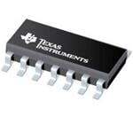
ICGOO在线商城 > 集成电路(IC) > 逻辑 - 栅极和逆变器 > SN74LV05ADR
 Datasheet下载
- 型号: SN74LV05ADR
- 制造商: Texas Instruments
- 库位|库存: xxxx|xxxx
- 要求:
| 数量阶梯 | 香港交货 | 国内含税 |
| +xxxx | $xxxx | ¥xxxx |
查看当月历史价格
查看今年历史价格
SN74LV05ADR产品简介:
ICGOO电子元器件商城为您提供SN74LV05ADR由Texas Instruments设计生产,在icgoo商城现货销售,并且可以通过原厂、代理商等渠道进行代购。 SN74LV05ADR价格参考。Texas InstrumentsSN74LV05ADR封装/规格:逻辑 - 栅极和逆变器, Inverter IC 6 Channel Open Drain 14-SOIC。您可以下载SN74LV05ADR参考资料、Datasheet数据手册功能说明书,资料中有SN74LV05ADR 详细功能的应用电路图电压和使用方法及教程。
SN74LV05ADR是Texas Instruments(德州仪器)生产的一款逻辑电路,具体属于栅极和逆变器类别。该型号为单通道高速CMOS施密特触发反相器,采用低电压工艺设计,适用于多种应用场景。

 主要特性
1. 低电压操作:工作电压范围为1.65V至5.5V,适应不同的电源需求。
2. 施密特触发特性:具有回差特性,能够有效抑制输入信号的噪声,确保输出稳定。
3. 高抗干扰能力:适合在电磁干扰较强的环境中使用。
4. 低功耗:静态电流非常小,有助于延长电池寿命。
5. 快速响应:具备较高的开关速度,适用于高速数字电路。

 应用场景

 1. 信号整形
   - 用途:用于将不规则或噪声较大的输入信号转换为清晰的方波信号。
   - 例子:在传感器信号处理中,将来自传感器的模拟信号转换为数字信号,以驱动后续的数字电路。

 2. 电平转换
   - 用途:实现不同电压电平之间的转换。
   - 例子:在混合信号系统中,将3.3V信号转换为5V信号,或者反之,确保不同电压系统的兼容性。

 3. 时钟信号处理
   - 用途:对时钟信号进行整形和缓冲,确保时钟信号的稳定性和完整性。
   - 例子:在微控制器或FPGA系统中,用于处理外部时钟源,确保时钟信号的质量。

 4. 噪声抑制
   - 用途:通过施密特触发特性,有效抑制输入信号中的噪声,提高系统的抗干扰能力。
   - 例子:在工业控制、汽车电子等恶劣环境中,防止噪声对系统的影响。

 5. 接口电路
   - 用途:作为接口电路中的逻辑元件,用于数据传输和信号处理。
   - 例子:在通信模块中,用于处理串行数据的接收和发送,确保数据的准确性和完整性。

总之,SN74LV05ADR凭借其低电压操作、施密特触发特性、高抗干扰能力和快速响应等特点,广泛应用于信号整形、电平转换、时钟信号处理、噪声抑制以及接口电路等多种场合,特别是在需要高可靠性和稳定性的系统中表现出色。
| 参数 | 数值 |
| 产品目录 | 集成电路 (IC)半导体 |
| 描述 | IC HEX INVERT W/OD 14-SOIC变换器 Hex w/ OD Out |
| 产品分类 | |
| 品牌 | Texas Instruments |
| 产品手册 | |
| 产品图片 |
|
| rohs | 符合RoHS无铅 / 符合限制有害物质指令(RoHS)规范要求 |
| 产品系列 | 逻辑集成电路,变换器,Texas Instruments SN74LV05ADR74LV |
| 数据手册 | |
| 产品型号 | SN74LV05ADR |
| 不同V、最大CL时的最大传播延迟 | 7.5ns @ 5V,50pF |
| 产品目录页面 | |
| 产品种类 | 变换器 |
| 传播延迟时间 | 8.5 ns |
| 低电平输出电流 | 12 mA |
| 供应商器件封装 | 14-SOIC |
| 其它名称 | 296-3758-1 |
| 包装 | 剪切带 (CT) |
| 单位重量 | 129.400 mg |
| 商标 | Texas Instruments |
| 安装类型 | 表面贴装 |
| 安装风格 | SMD/SMT |
| 封装 | Reel |
| 封装/外壳 | 14-SOIC(0.154",3.90mm 宽) |
| 封装/箱体 | SOIC-14 |
| 工作温度 | -40°C ~ 85°C |
| 工作温度范围 | - 40 C to + 85 C |
| 工厂包装数量 | 2500 |
| 最大工作温度 | + 85 C |
| 最小工作温度 | - 40 C |
| 标准包装 | 1 |
| 特性 | 开路漏极 |
| 电压-电源 | 2 V ~ 5.5 V |
| 电流-输出高,低 | -,12mA |
| 电流-静态(最大值) | 20µA |
| 电源电压-最大 | 5.5 V |
| 电源电压-最小 | 2 V |
| 电路数 | 6 |
| 电路数量 | 6 Circuit |
| 系列 | SN74LV05A |
| 输入数 | 6 |
| 输入类型 | LVTTL |
| 输出类型 | CMOS |
| 逻辑电平-低 | 0.5V |
| 逻辑电平-高 | 1.5V |
| 逻辑类型 | |
| 逻辑系列 | LV-A |
| 高电平输出电流 | 0 mA |


PDF Datasheet 数据手册内容提取
Product Sample & Technical Tools & Support & Folder Buy Documents Software Community SN74LV05A SCLS391J–APRIL1998–REVISEDDECEMBER2014 SN74LV05A Hex Inverters With Open-Drain Outputs 1 Features 2 Applications • 2-Vto5.5-VV Operation • ElectronicPointsofSale 1 CC • TypicalV (OutputGroundBounce) • I/OModules:DigitalPLC/DCSInputs OLP <0.8VatVCC=3.3V,TA=25°C • MotorDrivesandControls • TypicalVOHV(OutputVOH Undershoot) • Servers >2.3VatV =3.3V,T =25°C CC A • NetworkSwitches • SupportMixed-ModeVoltageOperationonAll • TestsandMeasurements Ports • I SupportsPartial-Power-DownModeOperation 3 Description off • Latch-UpPerformanceExceeds250mAPer The SN74LV05A device contains six independent JESD17 invertersdesignedfor2-Vto5.5-VV operation. CC • ESDProtectionExceedsJESD22 ThisdeviceperformstheBooleanfunctionY= A. – 2500-VHuman-BodyModel DeviceInformation(1) – 200-VMachineModel PARTNUMBER PACKAGE BODYSIZE(NOM) – 2000-VCharged-DeviceModel TVSOP(14) 3.60mmx4.40mm SOIC(14) 8.65mm×3.91mm SN74LV05A SOP(14) 10.30mmx5.30mm SSOP(14) 6.20mmx5.30mm TSSOP(14) 5.00mmx4.40mm (1) For all available packages, see the orderable addendum at theendofthedatasheet. 4 Simplified Schematic A Y 1 An IMPORTANT NOTICE at the end of this data sheet addresses availability, warranty, changes, use in safety-critical applications, intellectualpropertymattersandotherimportantdisclaimers.PRODUCTIONDATA.
SN74LV05A SCLS391J–APRIL1998–REVISEDDECEMBER2014 www.ti.com Table of Contents 1 Features.................................................................. 1 9 DetailedDescription.............................................. 8 2 Applications........................................................... 1 9.1 Overview...................................................................8 3 Description............................................................. 1 9.2 FunctionalBlockDiagram.........................................8 4 SimplifiedSchematic............................................. 1 9.3 FeatureDescription...................................................8 9.4 DeviceFunctionalModes..........................................8 5 RevisionHistory..................................................... 2 10 ApplicationandImplementation.......................... 9 6 PinConfigurationandFunctions......................... 3 10.1 ApplicationInformation............................................9 7 Specifications......................................................... 4 10.2 TypicalApplication .................................................9 7.1 AbsoluteMaximumRatings......................................4 11 PowerSupplyRecommendations..................... 10 7.2 ESDRatings..............................................................4 12 Layout................................................................... 11 7.3 RecommendedOperatingConditions.......................5 7.4 ThermalInformation..................................................5 12.1 LayoutGuidelines.................................................11 7.5 ElectricalCharacteristics...........................................5 12.2 LayoutExample....................................................11 7.6 SwitchingCharacteristics,V =2.5V±0.2V........6 13 DeviceandDocumentationSupport................. 11 CC 7.7 SwitchingCharacteristics,V =3.3V±0.3V........6 13.1 RelatedLinks........................................................11 CC 7.8 SwitchingCharacteristics,V =5V±0.5V...........6 13.2 Trademarks...........................................................11 CC 7.9 NoiseCharacteristics................................................6 13.3 ElectrostaticDischargeCaution............................11 7.10 OperatingCharacteristics........................................6 13.4 Glossary................................................................11 7.11 TypicalCharacteristics............................................7 14 Mechanical,Packaging,andOrderable Information........................................................... 11 8 ParameterMeasurementInformation..................7 5 Revision History ChangesfromRevisionI(April2005)toRevisionJ Page • AddedApplications,DeviceInformationtable,PinFunctionstable,ESDRatingstable,ThermalInformationtable, TypicalCharacteristics,FeatureDescriptionsection,DeviceFunctionalModes,ApplicationandImplementation section,PowerSupplyRecommendationssection,Layoutsection,DeviceandDocumentationSupportsection,and Mechanical,Packaging,andOrderableInformationsection.................................................................................................. 1 • DeletedOrderingInformationtable........................................................................................................................................ 1 • MAXoperatingtemperatureto125°CinRecommendedOperatingConditionstable........................................................... 5 2 SubmitDocumentationFeedback Copyright©1998–2014,TexasInstrumentsIncorporated ProductFolderLinks:SN74LV05A
SN74LV05A www.ti.com SCLS391J–APRIL1998–REVISEDDECEMBER2014 6 Pin Configuration and Functions SN74LV05A...D,DB,DGV,NS,ORPWPACKAGE (TOPVIEW) 1A 1 14 VCC 1Y 2 13 6A 2A 3 12 6Y 2Y 4 11 5A 3A 5 10 5Y 3Y 6 9 4A GND 7 8 4Y PinFunctions PIN TYPE DESCRIPTION NO. NAME 1 1A I 1AInput 2 1Y O 1YOutput 3 2A I 2AInput 4 2Y O 2YOutput 5 3A I 3AInput 6 3Y O 3YOutput 7 GND — GroundPin 8 4Y O 4YOutput 9 4A I 4AInput 10 5Y O 5YOutput 11 5A I 5AInput 12 6Y O 6YOutput 13 6A I 6AInput 14 V — PowerPin CC Copyright©1998–2014,TexasInstrumentsIncorporated SubmitDocumentationFeedback 3 ProductFolderLinks:SN74LV05A
SN74LV05A SCLS391J–APRIL1998–REVISEDDECEMBER2014 www.ti.com 7 Specifications 7.1 Absolute Maximum Ratings overoperatingfree-airtemperaturerange(unlessotherwisenoted)(1) MIN MAX UNIT V Supplyvoltagerange –0.5 7 V CC V Inputvoltagerange(2) –0.5 7 V I V Voltagerangeappliedtoanyoutputinthehigh-impedanceorpower-offstate(2) –0.5 7 V O V Outputvoltagerange(2)(3) –0.5 V +0.5 V O CC I Inputclampcurrent V <0 –20 mA IK I I Outputclampcurrent V <0 –50 mA OK O I Continuousoutputcurrent V =0toV ±25 mA O O CC ContinuouscurrentthroughV orGND ±50 mA CC T Storagetemperaturerange –65 150 °C stg (1) StressesbeyondthoselistedunderAbsoluteMaximumRatingsmaycausepermanentdamagetothedevice.Thesearestressratings only,andfunctionaloperationofthedeviceattheseoranyotherconditionsbeyondthoseindicatedunderRecommendedOperating Conditionsisnotimplied.Exposuretoabsolute-maximum-ratedconditionsforextendedperiodsmayaffectdevicereliability. (2) Theinputandoutputnegative-voltageratingsmaybeexceedediftheinputandoutputcurrentratingsareobserved. (3) Thisvalueislimitedto5.5-Vmaximum. 7.2 ESD Ratings VALUE UNIT Humanbodymodel(HBM),perANSI/ESDA/JEDECJS-001,allpins(1) 2500 V(ESD) Electrostaticdischarge Chargeddevicemodel(CDM),perJEDECspecificationJESD22-C101, V allpins(2) 2000 (1) JEDECdocumentJEP155statesthat500-VHBMallowssafemanufacturingwithastandardESDcontrolprocess. (2) JEDECdocumentJEP157statesthat250-VCDMallowssafemanufacturingwithastandardESDcontrolprocess. 4 SubmitDocumentationFeedback Copyright©1998–2014,TexasInstrumentsIncorporated ProductFolderLinks:SN74LV05A
SN74LV05A www.ti.com SCLS391J–APRIL1998–REVISEDDECEMBER2014 7.3 Recommended Operating Conditions overoperatingfree-airtemperaturerange(unlessotherwisenoted)(1) MIN MAX UNIT V Supplyvoltage 2 5.5 V CC V =2V 1.5 CC V =2.3Vto2.7V V ×0.7 CC CC V High-levelinputvoltage V IH V =3Vto3.6V V ×0.7 CC CC V =4.5Vto5.5V V ×0.7 CC CC V =2V 0.5 CC V =2.3Vto2.7V V ×0.3 CC CC V Low-levelinputvoltage V IL V =3Vto3.6V V ×0.3 CC CC V =4.5Vto5.5V V ×0.3 CC CC V Inputvoltage 0 5.5 V I V Outputvoltage 0 5.5 V O V =2V 50 µA CC V =2.3Vto2.7V 2 CC I Low-leveloutputcurrent OL V =3Vto3.6V 6 mA CC V =4.5Vto5.5V 12 CC V =2.3Vto2.7V 200 CC Δt/Δv Inputtransitionriseorfallrate V =3Vto3.6V 100 ns/V CC V =4.5Vto5.5V 20 CC T Operatingfree-airtemperature –40 125 °C A (1) AllunusedinputsofthedevicemustbeheldatV orGNDtoensureproperdeviceoperation.RefertotheTIapplicationreport, CC ImplicationsofSloworFloatingCMOSInputs(SCBA004). 7.4 Thermal Information SN74LV05A THERMALMETRIC(1) D DB DGV NS PW UNIT 14PINS R Junction-to-ambientthermalresistance 94.9 107.4 130.4 91.4 122.6 θJA R Junction-to-case(top)thermalresistance 56.3 59.9 53.4 49.0 51.3 θJC(top) R Junction-to-boardthermalresistance 49.2 54.7 63.5 50.2 64.4 °C/W θJB ψ Junction-to-topcharacterizationparameter 20.7 21.0 7.3 15.3 6.8 JT ψ Junction-to-boardcharacterizationparameter 48.9 51.2 62.8 49.8 63.8 JB (1) Formoreinformationabouttraditionalandnewthermalmetrics,seetheICPackageThermalMetricsapplicationreport(SPRA953). 7.5 Electrical Characteristics overrecommendedoperatingfree-airtemperaturerange(unlessotherwisenoted) T =25°C –40°Cto85°C –40°Cto125°C A PARAMETER TESTCONDITIONS V UNIT CC MIN TYP MAX MIN MAX MIN MAX 2Vto I =50µA 0.1 0.1 0.1 OL 5.5V VOL IOL=2mA 2.3V 0.4 0.4 0.4 V I =6mA 3V 0.44 0.44 0.44 OL I =12mA 4.5V 0.55 0.55 0.6 OL 0to I V =5.5VorGND ±1 ±1 ±1 µA I I 5.5V I V =V orGND, I =0 5.5 20 20 20 µA CC I CC O I V orV =0to5.5V 0 5 5 5 µA off I O C V =V orGND 3.3V 2.5 pF i I CC Copyright©1998–2014,TexasInstrumentsIncorporated SubmitDocumentationFeedback 5 ProductFolderLinks:SN74LV05A
SN74LV05A SCLS391J–APRIL1998–REVISEDDECEMBER2014 www.ti.com 7.6 Switching Characteristics, V = 2.5 V ± 0.2 V CC overrecommendedoperatingfree-airtemperaturerange(unlessotherwisenoted)(seeFigure3) FROM TO LOAD TA=25°C –40°Cto85°C –40°Cto125°C PARAMETER UNIT (INPUT) (OUTPUT) CAPACITANCE MIN TYP MAX MIN MAX MIN MAX t 3.6(1) 10.4(1) 1 13 1 13.5 PLH A Y C =15pF ns t L 5.8(1) 12.2(1) 1 15 1 16.5 PHL t 6.1 15.2 1 18 1 18.5 PLH A Y C =50pF ns L t 8.1 16.6 1 19.5 1 21 PHL (1) OnproductscomplianttoMIL-PRF-38535,thisparameterisnotproductiontested. 7.7 Switching Characteristics, V = 3.3 V ± 0.3 V CC overrecommendedoperatingfree-airtemperaturerange(unlessotherwisenoted)(seeFigure3) FROM TO LOAD TA=25°C –40°Cto85°C –40°Cto125°C PARAMETER UNIT (INPUT) (OUTPUT) CAPACITANCE MIN TYP MAX MIN MAX MIN MAX t 2.9(1) 7.1(1) 1 8.5 1 9 PLH A Y C =15pF ns t L 4(1) 7.1(1) 1 8.5 1 9.5 PHL t 4.7 10.6 1 12 1 12.5 PLH A Y C =50pF ns L t 5.8 10.6 1 12 1 13 PHL (1) OnproductscomplianttoMIL-PRF-38535,thisparameterisnotproductiontested. 7.8 Switching Characteristics, V = 5 V ± 0.5 V CC overrecommendedoperatingfree-airtemperaturerange(unlessotherwisenoted)(seeFigure3) FROM TO LOAD TA=25°C –40°Cto85°C –40°Cto125°C PARAMETER UNIT (INPUT) (OUTPUT) CAPACITANCE MIN TYP MAX MIN MAX MIN MAX t 2.2(1) 5.5(1) 1 6.5 1 7 PLH A Y C =15pF ns t L 2.9(1) 5.5(1) 1 6.5 1 7.5 PHL t 3.4 7.5 1 8.5 1 9 PLH A Y C =50pF ns L t 4.2 7.5 1 8.5 1 9.5 PHL (1) OnproductscomplianttoMIL-PRF-38535,thisparameterisnotproductiontested. 7.9 Noise Characteristics(1) V =3.3V,C =50pF,T =25°C CC L A SN74LV05A PARAMETER UNIT MIN TYP MAX V Quietoutput,maximumdynamicV 0.55 0.8 V OL(P) OL V Quietoutput,minimumdynamicV –0.04 –0.8 V OL(V) OL V Quietoutput,minimumdynamicV 3.12 V OH(V) OH V High-leveldynamicinputvoltage 2.31 V IH(D) V Low-leveldynamicinputvoltage 0.97 V IL(D) (1) Characteristicsareforsurface-mountpackagesonly. 7.10 Operating Characteristics T =25°C A PARAMETER TESTCONDITIONS V TYP UNIT CC 3.3V 2.5 C Powerdissipationcapacitance C =50pF, f=10MHz pF pd L 5V 3 6 SubmitDocumentationFeedback Copyright©1998–2014,TexasInstrumentsIncorporated ProductFolderLinks:SN74LV05A
SN74LV05A www.ti.com SCLS391J–APRIL1998–REVISEDDECEMBER2014 7.11 Typical Characteristics 4 7 TPD in ns 3.5 6 3 5 2.5 s) s) 4 n n D ( 2 D ( P P 3 T T 1.5 2 1 0.5 1 TPD in ns 0 0 -100 -50 0 50 100 150 0 1 2 3 4 5 6 Temperature (qC) D001 VCC D001 Figure1.TPDvsTemperature Figure2.TPDvsV at25°C CC 8 Parameter Measurement Information VCC VCC RL= 1 kΩ Input 50% VCC 50% VCC 0V From Output Test UnderTest Point tPHL tPLH CL ≈VCC (see NoteA) Output 50% VCC VOL+0.3V VOL LOAD CIRCUIT FOR VOLTAGEWAVEFORMS OPEN-DRAIN OUTPUTS PROPAGATIONDELAYTIMES NOTES: A. CLincludes probe and jig capacitance. B. Allinputpulsesaresuppliedbygeneratorshavingthefollowingcharacteristics: PRR≤1 MHz, ZO= 50Ω, tr≤3ns,tf≤3 ns. C. Theoutputsaremeasuredoneatatime,withoneinputtransitionpermeasurement. Figure3. LoadCircuitandVoltageWaveforms Copyright©1998–2014,TexasInstrumentsIncorporated SubmitDocumentationFeedback 7 ProductFolderLinks:SN74LV05A
SN74LV05A SCLS391J–APRIL1998–REVISEDDECEMBER2014 www.ti.com 9 Detailed Description 9.1 Overview TheSN74LV05Adevicecontainssixindependentinvertersdesignedfor2-Vto5.5-VV operation. CC ThisdeviceperformstheBooleanfunctionY= A. The open-drain outputs require pull-up resistors to perform correctly and can be connected to other open-drain outputstoimplementactive-low,wired-ORoractive-highwired-ANDfunctions. This device is fully specified for partial-power-down applications using I . The I circuitry disables the outputs, off off preventingdamagingcurrentbackflowthroughthedevicewhenitispowereddown. 9.2 Functional Block Diagram A Y Figure4. LogicDiagram(PositiveLogic) 9.3 Feature Description • Wideoperatingvoltagerange – Operatesfrom2Vto5.5V • Allowsdown-voltagetranslation – Inputsacceptvoltagesto5.5V • I feature off – AllowsvoltagesontheinputsandoutputswhenV is0V CC 9.4 Device Functional Modes Table1.FunctionTable (EachInverter) INPUT OUTPUT A Y H L L H 8 SubmitDocumentationFeedback Copyright©1998–2014,TexasInstrumentsIncorporated ProductFolderLinks:SN74LV05A
SN74LV05A www.ti.com SCLS391J–APRIL1998–REVISEDDECEMBER2014 10 Application and Implementation NOTE Information in the following applications sections is not part of the TI component specification, and TI does not warrant its accuracy or completeness. TI’s customers are responsible for determining suitability of components for their purposes. Customers should validateandtesttheirdesignimplementationtoconfirmsystemfunctionality. 10.1 Application Information SN74LV05A is a low-drive, open-drain CMOS device that can be used for a multitude of buffer type functions. The inputs are 5.5-V tolerant and the outputs are open-drain and 5.5-V tolerant, allowing it to translate up to 5.5 VordowntoanyothervoltagebetweenGNDand5.5V. 10.2 Typical Application Buffer Function Basic LED Driver VPU VPU Wired OR μC or Logic μC or Logic μC or Logic LV05A LV05A μC or Logic LV05A Figure5. TypicalApplicationSchematic 10.2.1 DesignRequirements This device uses CMOS technology and has balanced output drive. Care should be taken to avoid bus contention because it can drive currents that would exceed maximum limits. The high drive will also create fast edgesintolightloads,soroutingandloadconditionsshouldbeconsideredtopreventringing. 10.2.2 DetailedDesignProcedure 1. RecommendedInputConditions – Forrisetimeandfalltimespecifications,see Δt/ΔVintheRecommendedOperatingConditions table. – ForspecifiedHighandlowlevels,seeV andV intheRecommendedOperatingConditions table. IH IL – Inputsareovervoltagetolerantallowingthemtogoashighas5.5VatanyvalidV . CC 2. RecommendOutputConditions – Loadcurrentsshouldnotexceed35mAperoutputand50mAtotalforthepart. Copyright©1998–2014,TexasInstrumentsIncorporated SubmitDocumentationFeedback 9 ProductFolderLinks:SN74LV05A
SN74LV05A SCLS391J–APRIL1998–REVISEDDECEMBER2014 www.ti.com Typical Application (continued) 10.2.3 ApplicationCurves 3.5 VOUT input high 3 VOUT input low 2.5 2 CC 1.5 V 1 0.5 0 -0.5 0 0.5 1 1.5 2 2.5 3 3.5 4 VOUT D001 Figure6.OutputatPowerUpwith4kPull-Up3.3V 11 Power Supply Recommendations The power supply can be any voltage between the MIN and MAX supply voltage rating located in the RecommendedOperatingConditionstable. Each V pin should have a good bypass capacitor to prevent power disturbance. For devices with a single CC supply, 0.1 μF is recommended. If there are multiple V pins, 0.01 μF or 0.022 μF is recommended for each CC power pin. It is acceptable to parallel multiple bypass caps to reject different frequencies of noise. A 0.1 μF and 1 μF are commonly used in parallel. The bypass capacitor should be installed as close to the power pin as possibleforbestresults. 10 SubmitDocumentationFeedback Copyright©1998–2014,TexasInstrumentsIncorporated ProductFolderLinks:SN74LV05A
SN74LV05A www.ti.com SCLS391J–APRIL1998–REVISEDDECEMBER2014 12 Layout 12.1 Layout Guidelines When using multiple bit logic devices, inputs should not float. In many cases, functions or parts of functions of digital logic devices are unused. Some examples are when only two inputs of a triple-input AND gate are used, or when only 3 of the 4-buffer gates are used. Such input pins should not be left unconnected because the undefinedvoltagesattheoutsideconnectionsresultinundefinedoperationalstates. Specified in Figure 7 are rules that must be observed under all circumstances. All unused inputs of digital logic devices must be connected to a high or low bias to prevent them from floating. The logic level that should be applied to any particular unused input depends on the function of the device. Generally they will be tied to GND or V , whichever makes more sense or is more convenient. It is acceptable to float outputs unless the part is a CC transceiver. 12.2 Layout Example V cc Input Unused Input Output Unused Input Output Input Figure7. LayoutDiagram 13 Device and Documentation Support 13.1 Related Links The table below lists quick access links. Categories include technical documents, support and community resources,toolsandsoftware,andquickaccesstosampleorbuy. Table2.RelatedLinks TECHNICAL TOOLS& SUPPORT& PARTS PRODUCTFOLDER SAMPLE&BUY DOCUMENTS SOFTWARE COMMUNITY SN74LV05A Clickhere Clickhere Clickhere Clickhere Clickhere 13.2 Trademarks Alltrademarksarethepropertyoftheirrespectiveowners. 13.3 Electrostatic Discharge Caution Thesedeviceshavelimitedbuilt-inESDprotection.Theleadsshouldbeshortedtogetherorthedeviceplacedinconductivefoam duringstorageorhandlingtopreventelectrostaticdamagetotheMOSgates. 13.4 Glossary SLYZ022—TIGlossary. Thisglossarylistsandexplainsterms,acronyms,anddefinitions. 14 Mechanical, Packaging, and Orderable Information The following pages include mechanical, packaging, and orderable information. This information is the most current data available for the designated devices. This data is subject to change without notice and revision of thisdocument.Forbrowser-basedversionsofthisdatasheet,refertotheleft-handnavigation. Copyright©1998–2014,TexasInstrumentsIncorporated SubmitDocumentationFeedback 11 ProductFolderLinks:SN74LV05A
PACKAGE OPTION ADDENDUM www.ti.com 6-Feb-2020 PACKAGING INFORMATION Orderable Device Status Package Type Package Pins Package Eco Plan Lead/Ball Finish MSL Peak Temp Op Temp (°C) Device Marking Samples (1) Drawing Qty (2) (6) (3) (4/5) SN74LV05AD ACTIVE SOIC D 14 50 Green (RoHS NIPDAU Level-1-260C-UNLIM -40 to 125 LV05A & no Sb/Br) SN74LV05ADGVR ACTIVE TVSOP DGV 14 2000 Green (RoHS NIPDAU Level-1-260C-UNLIM -40 to 125 LV05A & no Sb/Br) SN74LV05ADR ACTIVE SOIC D 14 2500 Green (RoHS NIPDAU Level-1-260C-UNLIM -40 to 125 LV05A & no Sb/Br) SN74LV05ADRG4 ACTIVE SOIC D 14 2500 Green (RoHS NIPDAU Level-1-260C-UNLIM -40 to 125 LV05A & no Sb/Br) SN74LV05ANSR ACTIVE SO NS 14 2000 Green (RoHS NIPDAU Level-1-260C-UNLIM -40 to 125 74LV05A & no Sb/Br) SN74LV05APW ACTIVE TSSOP PW 14 90 Green (RoHS NIPDAU Level-1-260C-UNLIM -40 to 125 LV05A & no Sb/Br) SN74LV05APWR ACTIVE TSSOP PW 14 2000 Green (RoHS NIPDAU Level-1-260C-UNLIM -40 to 125 LV05A & no Sb/Br) SN74LV05APWT ACTIVE TSSOP PW 14 250 Green (RoHS NIPDAU Level-1-260C-UNLIM -40 to 125 LV05A & no Sb/Br) (1) The marketing status values are defined as follows: ACTIVE: Product device recommended for new designs. LIFEBUY: TI has announced that the device will be discontinued, and a lifetime-buy period is in effect. NRND: Not recommended for new designs. Device is in production to support existing customers, but TI does not recommend using this part in a new design. PREVIEW: Device has been announced but is not in production. Samples may or may not be available. OBSOLETE: TI has discontinued the production of the device. (2) RoHS: TI defines "RoHS" to mean semiconductor products that are compliant with the current EU RoHS requirements for all 10 RoHS substances, including the requirement that RoHS substance do not exceed 0.1% by weight in homogeneous materials. Where designed to be soldered at high temperatures, "RoHS" products are suitable for use in specified lead-free processes. TI may reference these types of products as "Pb-Free". RoHS Exempt: TI defines "RoHS Exempt" to mean products that contain lead but are compliant with EU RoHS pursuant to a specific EU RoHS exemption. Green: TI defines "Green" to mean the content of Chlorine (Cl) and Bromine (Br) based flame retardants meet JS709B low halogen requirements of <=1000ppm threshold. Antimony trioxide based flame retardants must also meet the <=1000ppm threshold requirement. (3) MSL, Peak Temp. - The Moisture Sensitivity Level rating according to the JEDEC industry standard classifications, and peak solder temperature. (4) There may be additional marking, which relates to the logo, the lot trace code information, or the environmental category on the device. Addendum-Page 1
PACKAGE OPTION ADDENDUM www.ti.com 6-Feb-2020 (5) Multiple Device Markings will be inside parentheses. Only one Device Marking contained in parentheses and separated by a "~" will appear on a device. If a line is indented then it is a continuation of the previous line and the two combined represent the entire Device Marking for that device. (6) Lead/Ball Finish - Orderable Devices may have multiple material finish options. Finish options are separated by a vertical ruled line. Lead/Ball Finish values may wrap to two lines if the finish value exceeds the maximum column width. Important Information and Disclaimer:The information provided on this page represents TI's knowledge and belief as of the date that it is provided. TI bases its knowledge and belief on information provided by third parties, and makes no representation or warranty as to the accuracy of such information. Efforts are underway to better integrate information from third parties. TI has taken and continues to take reasonable steps to provide representative and accurate information but may not have conducted destructive testing or chemical analysis on incoming materials and chemicals. TI and TI suppliers consider certain information to be proprietary, and thus CAS numbers and other limited information may not be available for release. In no event shall TI's liability arising out of such information exceed the total purchase price of the TI part(s) at issue in this document sold by TI to Customer on an annual basis. Addendum-Page 2
PACKAGE MATERIALS INFORMATION www.ti.com 13-Dec-2013 TAPE AND REEL INFORMATION *Alldimensionsarenominal Device Package Package Pins SPQ Reel Reel A0 B0 K0 P1 W Pin1 Type Drawing Diameter Width (mm) (mm) (mm) (mm) (mm) Quadrant (mm) W1(mm) SN74LV05ADGVR TVSOP DGV 14 2000 330.0 12.4 6.8 4.0 1.6 8.0 12.0 Q1 SN74LV05ADR SOIC D 14 2500 330.0 16.4 6.5 9.0 2.1 8.0 16.0 Q1 SN74LV05ANSR SO NS 14 2000 330.0 16.4 8.2 10.5 2.5 12.0 16.0 Q1 SN74LV05APWR TSSOP PW 14 2000 330.0 12.4 6.9 5.6 1.6 8.0 12.0 Q1 SN74LV05APWT TSSOP PW 14 250 330.0 12.4 6.9 5.6 1.6 8.0 12.0 Q1 PackMaterials-Page1
PACKAGE MATERIALS INFORMATION www.ti.com 13-Dec-2013 *Alldimensionsarenominal Device PackageType PackageDrawing Pins SPQ Length(mm) Width(mm) Height(mm) SN74LV05ADGVR TVSOP DGV 14 2000 367.0 367.0 35.0 SN74LV05ADR SOIC D 14 2500 367.0 367.0 38.0 SN74LV05ANSR SO NS 14 2000 367.0 367.0 38.0 SN74LV05APWR TSSOP PW 14 2000 367.0 367.0 35.0 SN74LV05APWT TSSOP PW 14 250 367.0 367.0 35.0 PackMaterials-Page2
None
MECHANICAL DATA MPDS006C – FEBRUARY 1996 – REVISED AUGUST 2000 DGV (R-PDSO-G**) PLASTIC SMALL-OUTLINE 24 PINS SHOWN 0,23 0,40 0,07 M 0,13 24 13 0,16 NOM 4,50 6,60 4,30 6,20 Gage Plane 0,25 0°–(cid:1)8° 0,75 1 12 0,50 A Seating Plane 0,15 1,20 MAX 0,08 0,05 PINS ** 14 16 20 24 38 48 56 DIM A MAX 3,70 3,70 5,10 5,10 7,90 9,80 11,40 A MIN 3,50 3,50 4,90 4,90 7,70 9,60 11,20 4073251/E 08/00 NOTES: A. All linear dimensions are in millimeters. B. This drawing is subject to change without notice. C. Body dimensions do not include mold flash or protrusion, not to exceed 0,15 per side. D. Falls within JEDEC: 24/48 Pins – MO-153 14/16/20/56 Pins – MO-194 • POST OFFICE BOX 655303 DALLAS, TEXAS 75265
None
None
None
None
IMPORTANTNOTICEANDDISCLAIMER TI PROVIDES TECHNICAL AND RELIABILITY DATA (INCLUDING DATASHEETS), DESIGN RESOURCES (INCLUDING REFERENCE DESIGNS), APPLICATION OR OTHER DESIGN ADVICE, WEB TOOLS, SAFETY INFORMATION, AND OTHER RESOURCES “AS IS” AND WITH ALL FAULTS, AND DISCLAIMS ALL WARRANTIES, EXPRESS AND IMPLIED, INCLUDING WITHOUT LIMITATION ANY IMPLIED WARRANTIES OF MERCHANTABILITY, FITNESS FOR A PARTICULAR PURPOSE OR NON-INFRINGEMENT OF THIRD PARTY INTELLECTUAL PROPERTY RIGHTS. These resources are intended for skilled developers designing with TI products. You are solely responsible for (1) selecting the appropriate TI products for your application, (2) designing, validating and testing your application, and (3) ensuring your application meets applicable standards, and any other safety, security, or other requirements. These resources are subject to change without notice. TI grants you permission to use these resources only for development of an application that uses the TI products described in the resource. Other reproduction and display of these resources is prohibited. No license is granted to any other TI intellectual property right or to any third party intellectual property right. TI disclaims responsibility for, and you will fully indemnify TI and its representatives against, any claims, damages, costs, losses, and liabilities arising out of your use of these resources. TI’s products are provided subject to TI’s Terms of Sale (www.ti.com/legal/termsofsale.html) or other applicable terms available either on ti.com or provided in conjunction with such TI products. TI’s provision of these resources does not expand or otherwise alter TI’s applicable warranties or warranty disclaimers for TI products. Mailing Address: Texas Instruments, Post Office Box 655303, Dallas, Texas 75265 Copyright © 2020, Texas Instruments Incorporated