ICGOO在线商城 > 集成电路(IC) > 逻辑 - 栅极和逆变器 > MM74HC86M
 Datasheet下载
- 型号: MM74HC86M
- 制造商: Fairchild Semiconductor
- 库位|库存: xxxx|xxxx
- 要求:
| 数量阶梯 | 香港交货 | 国内含税 |
| +xxxx | $xxxx | ¥xxxx |
查看当月历史价格
查看今年历史价格
MM74HC86M产品简介:
ICGOO电子元器件商城为您提供MM74HC86M由Fairchild Semiconductor设计生产,在icgoo商城现货销售,并且可以通过原厂、代理商等渠道进行代购。 MM74HC86M价格参考。Fairchild SemiconductorMM74HC86M封装/规格:逻辑 - 栅极和逆变器, XOR (Exclusive OR) IC 4 Channel 14-SOIC。您可以下载MM74HC86M参考资料、Datasheet数据手册功能说明书,资料中有MM74HC86M 详细功能的应用电路图电压和使用方法及教程。
ON Semiconductor的MM74HC86M属于逻辑 - 栅极和逆变器系列,是一款四路2输入异或(XOR)门电路。该器件采用高性能CMOS技术制造,适用于多种数字逻辑应用场景,以下为其主要应用领域:

1. 信号处理与比较
   MM74HC86M可以用于检测两个输入信号之间的差异,例如在数据传输中进行奇偶校验或错误检测。通过比较两路信号的状态,输出结果可用于判断信号一致性。

2. 脉冲生成与控制
   在时序电路中,该芯片可用于生成特定的脉冲信号。例如,在同步或异步计数器设计中,利用异或门的特性实现信号相位差检测或脉宽调制(PWM)功能。

3. 频率倍增与分频
   基于异或门的功能,MM74HC86M能够参与构建频率倍增或分频电路。通过组合多个异或门,可以实现复杂的时钟信号处理,满足通信、音频或其他需要精确时钟的应用需求。

4. 加法器与算术逻辑单元(ALU)设计
   异或门是全加器电路的核心组件之一,用于计算二进制加法中的“和”部分。MM74HC86M可广泛应用于微处理器、计算器或其他数字系统中的算术运算模块。

5. 数据加密与解密
   在简单加密算法中,异或操作常被用作基础逻辑运算。MM74HC86M可以实现数据流与密钥之间的逐位异或操作,从而完成加密或解密过程。

6. 传感器信号处理
   在工业自动化或消费电子领域,该芯片可用于处理来自传感器的数字信号。例如,检测开关状态变化或对多路输入信号进行逻辑组合。

7. 通信系统中的编码与解码
   MM74HC86M适用于简单的编码和解码任务,例如曼彻斯特编码/解码、差分信号转换等,以提高数据传输的可靠性和抗干扰能力。

总之,MM74HC86M凭借其低功耗、高稳定性和广泛的电压兼容性,成为各类数字逻辑电路设计中的重要元件,尤其适合需要高效信号处理和逻辑运算的应用场景。
| 参数 | 数值 |
| 产品目录 | 集成电路 (IC)半导体 |
| 描述 | IC GATE XOR 4CH 2-INP 14-SOIC逻辑门 Quad 2-Input OR Gate |
| 产品分类 | |
| 品牌 | Fairchild Semiconductor |
| 产品手册 | |
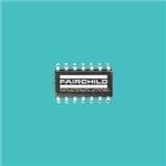
| 产品图片 |
|
| rohs | 符合RoHS无铅 / 符合限制有害物质指令(RoHS)规范要求 |
| 产品系列 | 逻辑集成电路,逻辑门,Fairchild Semiconductor MM74HC86M74HC |
| 数据手册 | |
| 产品型号 | MM74HC86M |
| 不同V、最大CL时的最大传播延迟 | 20ns @ 6V,50pF |
| 产品 | XOR |
| 产品目录页面 | |
| 产品种类 | 逻辑门 |
| 传播延迟时间 | 120 ns |
| 低电平输出电流 | 5.2 mA |
| 供应商器件封装 | 14-SOIC |
| 其它名称 | MM74HC86MFS |
| 包装 | 管件 |
| 单位重量 | 241 mg |
| 商标 | Fairchild Semiconductor |
| 安装类型 | 表面贴装 |
| 安装风格 | SMD/SMT |
| 封装 | Tube |
| 封装/外壳 | 14-SOIC(0.154",3.90mm 宽) |
| 封装/箱体 | SOIC-14 |
| 工作温度 | -40°C ~ 85°C |
| 工厂包装数量 | 55 |
| 最大工作温度 | + 85 C |
| 最小工作温度 | - 40 C |
| 栅极数量 | 4 Gate |
| 标准包装 | 55 |
| 特性 | - |
| 电压-电源 | 2 V ~ 6 V |
| 电流-输出高,低 | 5.2mA,5.2mA |
| 电流-静态(最大值) | 2µA |
| 电源电压-最大 | 6 V |
| 电源电压-最小 | 2 V |
| 电路数 | 4 |
| 系列 | MM74HC86 |
| 输入/输出线数量 | 2 / 1 |
| 输入数 | 2 |
| 输入线路数量 | 2 |
| 输出线路数量 | 1 |
| 逻辑电平-低 | 0.5 V ~ 1.8 V |
| 逻辑电平-高 | 1.5 V ~ 4.2 V |
| 逻辑类型 | XOR(异或) |
| 逻辑系列 | 74HC |
| 零件号别名 | MM74HC86M_NL |
| 高电平输出电流 | - 5.2 mA |


PDF Datasheet 数据手册内容提取
Is Now Part of To learn more about ON Semiconductor, please visit our website at www.onsemi.com Please note: As part of the Fairchild Semiconductor integration, some of the Fairchild orderable part numbers will need to change in order to meet ON Semiconductor’s system requirements. Since the ON Semiconductor product management systems do not have the ability to manage part nomenclature that utilizes an underscore (_), the underscore (_) in the Fairchild part numbers will be changed to a dash (-). This document may contain device numbers with an underscore (_). Please check the ON Semiconductor website to verify the updated device numbers. The most current and up-to-date ordering information can be found at www.onsemi.com. Please email any questions regarding the system integration to Fairchild_questions@onsemi.com. ON Semiconductor and the ON Semiconductor logo are trademarks of Semiconductor Components Industries, LLC dba ON Semiconductor or its subsidiaries in the United States and/or other countries. ON Semiconductor owns the rights to a number of patents, trademarks, copyrights, trade secrets, and other intellectual property. A listing of ON Semiconductor’s product/patent coverage may be accessed at www.onsemi.com/site/pdf/Patent-Marking.pdf. ON Semiconductor reserves the right to make changes without further notice to any products herein. ON Semiconductor makes no warranty, representation or guarantee regarding the suitability of its products for any particular purpose, nor does ON Semiconductor assume any liability arising out of the application or use of any product or circuit, and specifically disclaims any and all liability, including without limitation special, consequential or incidental damages. Buyer is responsible for its products and applications using ON Semiconductor products, including compliance with all laws, regulations and safety requirements or standards, regardless of any support or applications information provided by ON Semiconductor. “Typical” parameters which may be provided in ON Semiconductor data sheets and/or specifications can and do vary in different applications and actual performance may vary over time. All operating parameters, including “Typicals” must be validated for each customer application by customer’s technical experts. ON Semiconductor does not convey any license under its patent rights nor the rights of others. ON Semiconductor products are not designed, intended, or authorized for use as a critical component in life support systems or any FDA Class 3 medical devices or medical devices with a same or similar classification in a foreign jurisdiction or any devices intended for implantation in the human body. Should Buyer purchase or use ON Semiconductor products for any such unintended or unauthorized application, Buyer shall indemnify and hold ON Semiconductor and its officers, employees, subsidiaries, affiliates, and distributors harmless against all claims, costs, damages, and expenses, and reasonable attorney fees arising out of, directly or indirectly, any claim of personal injury or death associated with such unintended or unauthorized use, even if such claim alleges that ON Semiconductor was negligent regarding the design or manufacture of the part. ON Semiconductor is an Equal Opportunity/Affirmative Action Employer. This literature is subject to all applicable copyright laws and is not for resale in any manner.
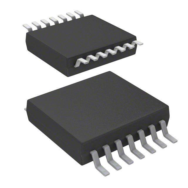
M M 7 4 H May 2012 C 8 6 — Q u MM74HC86 a d 2 Quad 2-Input Exclusive OR Gate - I n p u t E Description x Features c l The MM74HC86 exclusive OR gate utilizes advanced u Typical Propagation Delay: 9ns silicon-gate CMOS technology to achieve operating si v Wide Operating Voltage Range: 2–6V speeds similar to equivalent LS-TTL gates, while e maintaining the low power consumption and high noise O Low Input Current: 1mA Maximum immunity characteristic of standard CMOS integrated R Low Quiescent Current: 20mA Max. (74 Series) circuits. These gates are fully buffered and have a G fanout of 10 LS-TTL loads. The 74HC logic family is a Output Drive Capability: 10 LS-TTL Loads functionally as well as pin-out compatible with the te standard 74LS logic family. All inputs are protected from damage due to static discharge by internal diode clamps to V and ground. CC Table 1. Truth Table Inputs Outputs A B Y(1) L L L L H H H L H H H L Note: 1. Y ABABAB Figure 1. Pin Assignments (Top View) Ordering Information Operating Part Number Package Packing Method Temperature Range MM74HC86M 14-Lead, Small Outline Integrated Circuit Tube MM74HC86MX (SOIC), JEDEC MS-012, 0.150" Narrow Tape & Reel -40 to +85°C MM74HC86MTC 14-Lead, Thin Shrink Small Outline Package Tube MM74HC86MTCX (TSSOP), JEDEC MO-153, 4.4mm Wide Tape & Reel Note: 2. Pb-Free package per JEDEC J-STD-020B. © 1983 Fairchild Semiconductor Corporation www.fairchildsemi.com MM74HC86 • Rev. 1.4.0
M M Absolute Maximum Ratings 7 4 H Stresses exceeding the absolute maximum ratings may damage the device. The device may not function or be C operable above the recommended operating conditions and stressing the parts to these levels is not recommended. 8 6 In addition, extended exposure to stresses above the recommended operating conditions may affect device reliability. — Absolute maximum ratings are stress ratings only. Unless otherwise specified, all voltages are referenced to ground. Q Symbol Parameter Min. Max. Unit u a d V Supply Voltage -0.5 7.0 V CC 2 V DC Input Voltage -1.5 V +1.5 V - IN CC I n V DC Output Voltage -0.5 V +0.5 V p OUT CC u IIK, IOK Clamp Diode Current ±20 mA t E I DC Output Current, per Pin ±25 mA x OUT c ICC DC VCC or GND Current, per Pin ±50 mA lu s T Storage Temperature Range -65 +150 °C i STG v e TL Lead Temperature (Soldering, 10 Seconds) 260 °C O P Power Dissipation(3, 4) 600 mW R D G Note: a 3. Power dissipation temperature derating — plastic “N” package: -12 mW/°C from 65°C to 85°C. t e 4. S.O. package only 500mW. Recommended Operating Conditions The Recommended Operating Conditions table defines the conditions for actual device operation. Recommended operating conditions are specified to ensure optimal performance to the datasheet specifications. Fairchild does not recommend exceeding them or designing to Absolute Maximum Ratings. Symbol Parameter Conditions Min. Max. Unit V Supply Voltage 2 6 V CC V , V DC Input or Output Voltage 0 V V IN OUT CC T Operating Temperature Range -40 +85 °C A V = 2.0V 1000 CC t , t Input Rise or Fall Times V = 4.5V 500 ns R F CC V = 6.0V 400 CC © 1983 Fairchild Semiconductor Corporation www.fairchildsemi.com MM74HC86 • Rev. 1.4.0 2
M M DC Electrical Characteristics(5) 7 4 H T =-40 to T =-55 to C Symbol Parameter Condition V (V) TA=25°C A+85°C +A125°C Units 86 CC — Typ. Guaranteed Limit Q 2.0 1.5 1.5 1.5 u Minimum HIGH Level a VIH Input Voltage 4.5 3.15 3.15 3.15 V d 6.0 4.2 4.2 4.2 2 - I 2.0 0.5 0.5 0.5 n p Maximum LOW Level u V 4.5 1.35 1.35 1.35 V IL Input Voltage t E 6.0 1.8 1.8 1.8 x c l 2.0 2.0 1.9 1.9 1.9 u s V = V or V , IN IH IL i v |IOUT| ≤ 20µA 4.5 4.5 4.4 4.4 4.4 e VOH MOuintipmuut mVo HltaIGgHe Level 6.0 6.0 5.9 5.9 5.9 V OR VIN = VIH or VIL, 4.5 4.2 3.98 3.84 3.70 G |IOUT| ≤ 4.0mA a t V = V or V , e IN IH IL 6.0 5.7 5.48 5.34 5.20 |I | ≤ 5.2mA OUT 2.0 0 0.1 0.1 0.1 V = V or V , IN IH IL |IOUT| ≤ 20µA 4.5 0 0.1 0.1 0.1 Maximum LOW Level 6.0 0 0.1 0.1 0.1 V V OL Output Voltage V = V or V , IN IH IL 4.5 0.2 0.26 0.33 0.40 |I | ≤ 4.0mA OUT V = V or V , IN IH IL 6.0 0.2 0.26 0.33 0.40 |I | ≤ 5.2mA OUT I Maximum Input Current V = V or GND 6.0 ±0.1 ±1.0 ±1.0 mA IN IN CC Maximum Quiescent V = V or GND, I IN CC 6.0 2.0 20 40 mA CC Supply Current I = 0mA OUT Note: 5. For a power supply of 5V ±10%, the worst-case output voltages (V and V ) occur for HC at 4.5V. Thus, the OH OL 4.5V values should be used when designing with this supply. Worst-case V and V occur at V = 5.5V and IH IL CC 4.5V, respectively. (The V values at 5V and 5.5V are 3.5V and 3.85V, respectively.) The worst-case leakage IH current (I , I , and I ) occurs for CMOS at the higher voltage, so the 6.0V values should be used. IN CC OZ © 1983 Fairchild Semiconductor Corporation www.fairchildsemi.com MM74HC86 • Rev. 1.4.0 3
M M AC Electrical Characteristics 7 4 H T =-40 to T =-55 to C Symbol Parameter Conditions V TA=25°C A+85°C +A125°C Unit 86 CC s — Typ. Guaranteed Limit Q tPHL, tPLH Maximum Propagation Delay Ct L = = t 1 5=p 6Fn, s 5.0 12 20 ns ua R F d 2 2.0 60 120 151 179 -I n p u t tPHL, tPLH Maximum Propagation Delay 4.5 12 24 30 36 ns E x c l 6.0 10 20 26 30 u s i v e 2.0 30 75 95 110 O C = 50pF, L R Maximum Output Rise and tR = tF = 6ns G t , t 4.5 8 15 19 22 ns TLH THL Fall Time a t e 6.0 7 13 16 19 Power Dissipation CPD Capacitance (per Gate)(6) 25 pF C Maximum Input Capacitance 5 10 10 10 pF IN Note: 6. C determines the no-load dynamic power consumption, P = C V 2 f + I V , and the no load dynamic PD D PD CC CC CC current consumption, I = C V f + I . S PD CC CC © 1983 Fairchild Semiconductor Corporation www.fairchildsemi.com MM74HC86 • Rev. 1.4.0 4
0.65 (cid:24)(cid:17)(cid:19)(cid:19)(cid:147)(cid:19)(cid:17)(cid:20)(cid:19) A 0.43TYP 14 8 B 6.4 (cid:23)(cid:17)(cid:23)(cid:19)(cid:147)(cid:19)(cid:17)(cid:20)(cid:19) 6.10 3.2 1.65 1 7 0.2 C B A PIN1IDENT TOPVIEW ALLLEADTIPS 0.45 RECOMMENDEDLANDPATTERN 1.2MAX SEEDETAILA +0.15 0.90 -0.10 0.20 (cid:19)(cid:17)(cid:20)(cid:19)(cid:147)(cid:19)(cid:17)(cid:19)(cid:24) 0.09 ALLLEADTIPS 0.30 0.19 C 0.1 C 0.65 0.13 A B C (cid:20)(cid:21)(cid:17)(cid:19)(cid:19)(cid:131)(cid:3)(cid:55)(cid:50)(cid:51)(cid:3)(cid:9)(cid:3)(cid:37)(cid:50)(cid:55)(cid:55)(cid:50)(cid:48) FRONTVIEW 0.09MIN NOTES: GAGEPLANE A.CONFORMSTOJEDECREGISTRATIONMO-153, VARIATIONAB,REFNOTE6 B.DIMENSIONSAREINMILLIMETERS. 0.25 0.09MIN C.DIMENSIONSAREEXCLUSIVEOFBURRS, (cid:19)(cid:131)(cid:16)(cid:3)(cid:27)(cid:131) (cid:19)(cid:17)(cid:25)(cid:147)(cid:19)(cid:17)(cid:20) MOLDFLASH,ANDTIEBAREXTRUSIONS SEATINGPLANE 1.00 D.DIMENSIONINGANDTOLERANCESPERANSI DETAILA Y14.5M,2009. E.LANDPATTERNSTANDARD:SOP65P640X110-14M. F.DRAWINGFILENAME:MKT-MTC14rev7.
8.75 A 8.50 7.62 14 0.65 8 14 8 B 4.00 6.00 5.60 3.80 1.70 1 7 PIN #1 1.27 0.51 1 7 IDENT. 1.27 0.35 (0.33) 0.25 M C B A LAND PATTERN RECOMMENDATION TOP VIEW 1.75 MAX A C 0.25 0.19 1.50 0.10 C 0.25 1.25 0.10 SIDE VIEW FRONT VIEW NOTES: A. CONFORMS TO JEDEC MS-012, VARIATION AB, ISSUE C B. ALL DIMENSIONS ARE IN MILLIMETERS 0.50 0.25 x 45 C. DIMENSIONS DO NOT INCLUDE MOLD FLASH OR BURRS R0.10 GAGE D. LAND PATTERN STANDARD: PLANE SOIC127P600X145-14M R0.10 E. CONFORMS TO ASME Y14.5M, 2009 0.36 D. DRAWING FILENAME: MKT-M14Arev14 8° 0° 0.90 0.50 SEATING PLANE (1.04) DETAIL A SCALE 16 : 1
ON Semiconductor and are trademarks of Semiconductor Components Industries, LLC dba ON Semiconductor or its subsidiaries in the United States and/or other countries. ON Semiconductor owns the rights to a number of patents, trademarks, copyrights, trade secrets, and other intellectual property. A listing of ON Semiconductor’s product/patent coverage may be accessed at www.onsemi.com/site/pdf/Patent−Marking.pdf. ON Semiconductor reserves the right to make changes without further notice to any products herein. ON Semiconductor makes no warranty, representation or guarantee regarding the suitability of its products for any particular purpose, nor does ON Semiconductor assume any liability arising out of the application or use of any product or circuit, and specifically disclaims any and all liability, including without limitation special, consequential or incidental damages. Buyer is responsible for its products and applications using ON Semiconductor products, including compliance with all laws, regulations and safety requirements or standards, regardless of any support or applications information provided by ON Semiconductor. “Typical” parameters which may be provided in ON Semiconductor data sheets and/or specifications can and do vary in different applications and actual performance may vary over time. All operating parameters, including “Typicals” must be validated for each customer application by customer’s technical experts. ON Semiconductor does not convey any license under its patent rights nor the rights of others. ON Semiconductor products are not designed, intended, or authorized for use as a critical component in life support systems or any FDA Class 3 medical devices or medical devices with a same or similar classification in a foreign jurisdiction or any devices intended for implantation in the human body. Should Buyer purchase or use ON Semiconductor products for any such unintended or unauthorized application, Buyer shall indemnify and hold ON Semiconductor and its officers, employees, subsidiaries, affiliates, and distributors harmless against all claims, costs, damages, and expenses, and reasonable attorney fees arising out of, directly or indirectly, any claim of personal injury or death associated with such unintended or unauthorized use, even if such claim alleges that ON Semiconductor was negligent regarding the design or manufacture of the part. ON Semiconductor is an Equal Opportunity/Affirmative Action Employer. This literature is subject to all applicable copyright laws and is not for resale in any manner. PUBLICATION ORDERING INFORMATION LITERATURE FULFILLMENT: N. American Technical Support: 800−282−9855 Toll Free ON Semiconductor Website: www.onsemi.com Literature Distribution Center for ON Semiconductor USA/Canada 19521 E. 32nd Pkwy, Aurora, Colorado 80011 USA Europe, Middle East and Africa Technical Support: Order Literature: http://www.onsemi.com/orderlit Phone: 303−675−2175 or 800−344−3860 Toll Free USA/Canada Phone: 421 33 790 2910 Fax: 303−675−2176 or 800−344−3867 Toll Free USA/Canada Japan Customer Focus Center For additional information, please contact your local Email: orderlit@onsemi.com Phone: 81−3−5817−1050 Sales Representative © Semiconductor Components Industries, LLC www.onsemi.com www.onsemi.com 1
Mouser Electronics Authorized Distributor Click to View Pricing, Inventory, Delivery & Lifecycle Information: O N Semiconductor: MM74HC86N MM74HC86M MM74HC86SJ MM74HC86MX MM74HC86SJX MM74HC86MTC MM74HC86MTCX