ICGOO在线商城 > 集成电路(IC) > 逻辑 - 缓冲器,驱动器,接收器,收发器 > SN74HCT245DW

 Datasheet下载
- 型号: SN74HCT245DW
- 制造商: Texas Instruments
- 库位|库存: xxxx|xxxx
- 要求:
| 数量阶梯 | 香港交货 | 国内含税 |
| +xxxx | $xxxx | ¥xxxx |
查看当月历史价格
查看今年历史价格
SN74HCT245DW产品简介:
ICGOO电子元器件商城为您提供SN74HCT245DW由Texas Instruments设计生产,在icgoo商城现货销售,并且可以通过原厂、代理商等渠道进行代购。 SN74HCT245DW价格参考¥1.79-¥1.79。Texas InstrumentsSN74HCT245DW封装/规格:逻辑 - 缓冲器,驱动器,接收器,收发器, Transceiver, Non-Inverting 1 Element 8 Bit per Element 3-State Output 20-SOIC。您可以下载SN74HCT245DW参考资料、Datasheet数据手册功能说明书,资料中有SN74HCT245DW 详细功能的应用电路图电压和使用方法及教程。
SN74HCT245DW 是 Texas Instruments(德州仪器)生产的一款逻辑电路芯片,属于缓冲器/驱动器/接收器/收发器类别。它是一款8位总线收发器,支持三态输出功能,广泛应用于数据传输和信号转换的场景。以下是其主要应用场景:

 1. 数据总线扩展与隔离
   - SN74HCT245DW 可用于扩展微处理器或微控制器的数据总线。通过其三态输出功能,可以实现多路数据总线的共享,避免信号冲突。
   - 在复杂的系统中,它可以将不同模块的信号进行隔离,确保信号完整性。

 2. 电平转换
   - 该芯片支持 TTL 和 CMOS 电平兼容,能够在不同电压范围的设备之间进行信号转换。例如,在 5V 和 3.3V 系统之间传递数据时,SN74HCT245DW 可以作为电平转换器使用。

 3. 信号驱动增强
   - 在长距离信号传输或需要驱动多个负载的情况下,SN74HCT245DW 可以增强信号驱动能力,确保信号在传输过程中不失真。

 4. 计算机与外设接口
   - 该芯片常用于计算机与外设之间的数据传输。例如,在打印机、扫描仪或其他外部设备的接口设计中,SN74HCT245DW 可以实现双向数据通信。

 5. 工业控制与自动化
   - 在工业控制系统中,SN74HCT245DW 可用于实现主控单元与从属模块之间的数据交换,特别是在需要高可靠性和高速度的应用场合。

 6. 嵌入式系统设计
   - 在嵌入式系统中,这款芯片可用于管理多个外设的输入输出信号,提高系统的灵活性和可扩展性。

 7. 测试与测量设备
   - 在测试仪器中,SN74HCT245DW 可用于数据采集和处理模块之间的信号传输,确保测试结果的准确性和实时性。

总之,SN74HCT245DW 的应用场景非常广泛,适用于任何需要高效、可靠的双向数据传输和信号处理的电子系统设计。
| 参数 | 数值 |
| 产品目录 | 集成电路 (IC)半导体 |
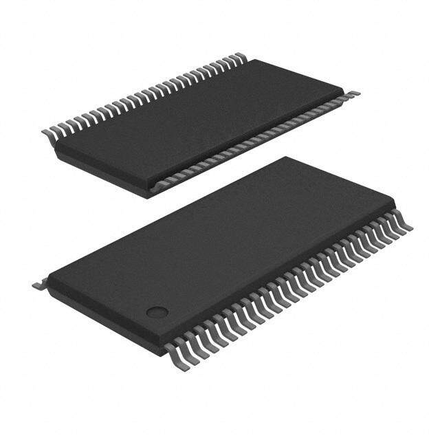
| 描述 | IC BUS TRANSCEIVER 8BIT 20SOIC总线收发器 Tri-State Octal Bus |
| 产品分类 | |
| 品牌 | Texas Instruments |
| 产品手册 | |
| 产品图片 |
|
| rohs | 符合RoHS无铅 / 符合限制有害物质指令(RoHS)规范要求 |
| 产品系列 | 逻辑集成电路,总线收发器,Texas Instruments SN74HCT245DW74HCT |
| 数据手册 | |
| 产品型号 | SN74HCT245DW |
| 产品目录页面 | |
| 产品种类 | 总线收发器 |
| 传播延迟时间 | 25 ns |
| 低电平输出电流 | 6 mA |
| 供应商器件封装 | 20-SOIC |
| 元件数 | 1 |
| 其它名称 | 296-1208-5 |
| 功能 | Tri-State Octal Bus |
| 包装 | 管件 |
| 单位重量 | 500.700 mg |
| 商标 | Texas Instruments |
| 安装类型 | 表面贴装 |
| 安装风格 | SMD/SMT |
| 封装 | Tube |
| 封装/外壳 | 20-SOIC(0.295",7.50mm 宽) |
| 封装/箱体 | SOIC-20 |
| 工作温度 | -40°C ~ 85°C |
| 工厂包装数量 | 25 |
| 最大工作温度 | + 85 C |
| 最小工作温度 | - 40 C |
| 极性 | Non-Inverting |
| 标准包装 | 25 |
| 每元件位数 | 8 |
| 每芯片的通道数量 | 8 |
| 电压-电源 | 4.5 V ~ 5.5 V |
| 电流-输出高,低 | 6mA,6mA |
| 电源电压-最大 | 5.5 V |
| 电源电压-最小 | 4.5 V |
| 电路数量 | 8 |
| 系列 | SN74HCT245 |
| 输入电平 | TTL |
| 输出电平 | CMOS |
| 输出类型 | 3-State |
| 逻辑类型 | 收发器,非反相 |
| 逻辑系列 | HCT |
| 高电平输出电流 | - 6 mA |


- 商务部:美国ITC正式对集成电路等产品启动337调查
- 曝三星4nm工艺存在良率问题 高通将骁龙8 Gen1或转产台积电
- 太阳诱电将投资9.5亿元在常州建新厂生产MLCC 预计2023年完工
- 英特尔发布欧洲新工厂建设计划 深化IDM 2.0 战略
- 台积电先进制程称霸业界 有大客户加持明年业绩稳了
- 达到5530亿美元!SIA预计今年全球半导体销售额将创下新高
- 英特尔拟将自动驾驶子公司Mobileye上市 估值或超500亿美元
- 三星加码芯片和SET,合并消费电子和移动部门,撤换高东真等 CEO
- 三星电子宣布重大人事变动 还合并消费电子和移动部门
- 海关总署:前11个月进口集成电路产品价值2.52万亿元 增长14.8%


PDF Datasheet 数据手册内容提取
Product Sample & Technical Tools & Support & Folder Buy Documents Software Community SN54HCT245,SN74HCT245 SCLS020F–MARCH1984–REVISEDAUGUST2016 SNx4HCT245 Octal Bus Transceivers With 3-State Outputs 1 Features 3 Description • OperatingVoltageRangeof4.5Vto5.5V The SNx4HCT245 octal bus transceivers are 1 designed for asynchronous two-way communication • High-Current3-StateOutputsDriveBusLines between data buses. The control-function DirectlyorupTo15-LSTTLLoads implementation minimizes external timing • LowPowerConsumption,80-µAMaximumI requirements. CC • Typicalt =14ns pd The SNx4HCT245 devices allow data transmission • ±6-mAOutputDriveat5V from the A bus to the B bus or from the B bus to the Abus,dependinguponthelogiclevelatthedirection- • LowInputCurrentof1 µAMaximum control (DIR) input. The output-enable (OE) input can • InputsAreTTL-VoltageCompatible be used to disable the device so that the buses are effectivelyisolated. 2 Applications • FactoryAutomationandControl DeviceInformation(1) • GridInfrastructure PARTNUMBER PACKAGE BODYSIZE(NOM) • ElectronicPointofSale SN54HCT245J CDIP(20) 24.20mm×6.92mm SN54HCT245FK LCCC(20) 8.89mm×8.89mm • Multi-FunctionPrinters SN54HCT245W CFP(20) 13.09mm×6.92mm • MotorDrives SN74HCT245DW SOIC(20) 12.80mm×7.50mm • Storage SN74HCT245N PDIP(20) 24.33mm×6.35mm • TelecomInfrastructure SN74HCT245NS SOP(20) 12.60mm×5.30mm SN74HCT245PW TSSOP(20) 6.50mm×4.40mm SN74HCT245DB SSOP(20) 7.80mm×7.20mm (1) For all available packages, see the orderable addendum at theendofthedatasheet. LogicDiagram(PositiveLogic) 1 DIR 19 OE 2 A1 18 B1 To Seven Other Channels Copyright © 2016, Texas Instruments Incorporated 1 An IMPORTANT NOTICE at the end of this data sheet addresses availability, warranty, changes, use in safety-critical applications, intellectualpropertymattersandotherimportantdisclaimers.PRODUCTIONDATA.
SN54HCT245,SN74HCT245 SCLS020F–MARCH1984–REVISEDAUGUST2016 www.ti.com Table of Contents 1 Features.................................................................. 1 8.3 FeatureDescription...................................................9 2 Applications........................................................... 1 8.4 DeviceFunctionalModes..........................................9 3 Description............................................................. 1 9 ApplicationandImplementation........................ 10 4 RevisionHistory..................................................... 2 9.1 ApplicationInformation............................................10 9.2 TypicalApplication .................................................10 5 PinConfigurationandFunctions......................... 3 10 PowerSupplyRecommendations..................... 12 6 Specifications......................................................... 4 11 Layout................................................................... 12 6.1 AbsoluteMaximumRatings......................................4 6.2 ESDRatings..............................................................4 11.1 LayoutGuidelines.................................................12 6.3 RecommendedOperatingConditions.......................4 11.2 LayoutExample....................................................12 6.4 ThermalInformation..................................................5 12 DeviceandDocumentationSupport................. 13 6.5 ElectricalCharacteristics...........................................5 12.1 DocumentationSupport........................................13 6.6 SwitchingCharacteristics:C =50pF......................6 12.2 RelatedLinks........................................................13 L 6.7 SwitchingCharacteristics:C =150pF....................7 12.3 ReceivingNotificationofDocumentationUpdates13 L 6.8 OperatingCharacteristics..........................................7 12.4 CommunityResource............................................13 6.9 TypicalCharacteristics..............................................7 12.5 Trademarks...........................................................13 7 ParameterMeasurementInformation..................8 12.6 ElectrostaticDischargeCaution............................13 12.7 Glossary................................................................13 8 DetailedDescription.............................................. 9 13 Mechanical,Packaging,andOrderable 8.1 Overview...................................................................9 Information........................................................... 13 8.2 FunctionalBlockDiagram.........................................9 4 Revision History NOTE:Pagenumbersforpreviousrevisionsmaydifferfrompagenumbersinthecurrentversion. ChangesfromRevisionE(August2003)toRevisionF Page • DeletedOrderingInformation,seePOAattheendofthedatasheet.................................................................................... 1 • AddedESDRatingstable,FeatureDescriptionsection,DeviceFunctionalModes,ApplicationandImplementation section,PowerSupplyRecommendationssection,Layoutsection,DeviceandDocumentationSupportsection,and Mechanical,Packaging,andOrderableInformationsection ................................................................................................. 1 • UpdatedvaluesintheThermalInformationtable................................................................................................................... 5 2 SubmitDocumentationFeedback Copyright©1984–2016,TexasInstrumentsIncorporated ProductFolderLinks:SN54HCT245 SN74HCT245
SN54HCT245,SN74HCT245 www.ti.com SCLS020F–MARCH1984–REVISEDAUGUST2016 5 Pin Configuration and Functions SN54HCT245...JORWPACKAGE SN74HCT245...DB,DW,N,NS,ORPWPACKAGE (TOPVIEW) DIR 1 20 VCC A1 2 19 OE A2 3 18 B1 A3 4 17 B2 A4 5 16 B3 A5 6 15 B4 A6 7 14 B5 A7 8 13 B6 A8 9 12 B7 GND 10 11 B8 SN54HCT245...FKPACKAGE (TOPVIEW) A2A1DIRVCCOE 3 2 1 2019 A3 4 18 B1 A4 5 17 B2 A5 6 16 B3 A6 7 15 B4 A7 8 14 B5 9 10111213 8D876 ANBBB G PinFunctions PIN I/O DESCRIPTION NO. NAME 1 DIR I Directionselect.High=AtoB,Low=BtoA 2 A1 I/O Channel1portA 3 A2 I/O Channel2portA 4 A3 I/O Channel3portA 5 A4 I/O Channel4portA 6 A5 I/O Channel5portA 7 A6 I/O Channel6portA 8 A7 I/O Channel7portA 9 A8 I/O Channel8portA 10 GND — Ground 11 B8 O/I Channel1portB 12 B7 O/I Channel2portB 13 B6 O/I Channel3portB 14 B5 O/I Channel4portB 15 B4 O/I Channel5portB 16 B3 O/I Channel6portB 17 B2 O/I Channel7portB 18 B1 O/I Channel8portB 19 OE I Outputenable,activelow.High=allportsinhighimpedancemode,Low=allportsactive 20 V — Powersupply CC Copyright©1984–2016,TexasInstrumentsIncorporated SubmitDocumentationFeedback 3 ProductFolderLinks:SN54HCT245 SN74HCT245
SN54HCT245,SN74HCT245 SCLS020F–MARCH1984–REVISEDAUGUST2016 www.ti.com 6 Specifications 6.1 Absolute Maximum Ratings overoperatingfree-airtemperaturerange(unlessotherwisenoted)(1) MIN MAX UNIT V Supplyvoltage –0.5 7 V CC I Inputclampcurrent(2) V <0orV >V ±20 mA IK I I CC I Outputclampcurrent(2) V <0orV >V ±20 mA OK O O CC I Continuousoutputcurrent V =0toV ±35 mA O O CC ContinuouscurrentthroughV orGND ±70 mA CC T Operatingvirtualjunctiontemperature 150 °C J T Storagetemperature –65 150 °C stg (1) StressesbeyondthoselistedunderAbsoluteMaximumRatingsmaycausepermanentdamagetothedevice.Thesearestressratings only,whichdonotimplyfunctionaloperationofthedeviceattheseoranyotherconditionsbeyondthoseindicatedunderRecommended OperatingConditions.Exposuretoabsolute-maximum-ratedconditionsforextendedperiodsmayaffectdevicereliability. (2) Theinputandoutputvoltageratingsmaybeexceedediftheinputandoutputcurrentratingsareobserved. 6.2 ESD Ratings VALUE UNIT Human-bodymodel(HBM),perANSI/ESDA/JEDECJS-001(1) ±1500 V(ESD) Electrostaticdischarge Charged-devicemodel(CDM),perJEDECspecificationJESD22- V C101(2) ±2000 (1) JEDECdocumentJEP155statesthat500-VHBMallowssafemanufacturingwithastandardESDcontrolprocess. (2) JEDECdocumentJEP157statesthat250-VCDMallowssafemanufacturingwithastandardESDcontrolprocess. 6.3 Recommended Operating Conditions overoperatingfree-airtemperaturerange(unlessotherwisenoted)(1) MIN NOM MAX UNIT V Supplyvoltage 4.5 5 5.5 V CC V High-levelinputvoltage V =4.5Vto5.5V 2 V IH CC V Low-levelinputvoltage V =4.5Vto5.5V 0.8 V IL CC V Inputvoltage 0 V V I CC V Outputvoltage 0 V V O CC Δt/Δv Inputtransitionriseandfalltime 500 ns SN54HCT245 –55 125 T Operatingfree-airtemperature °C A SN74HCT245 –40 85 (1) AllunusedinputsofthedevicemustbeheldatV orGNDtoensureproperdeviceoperation.SeetheTIapplicationreport, CC ImplicationsofSloworFloatingCMOSInputs(SCBA004). 4 SubmitDocumentationFeedback Copyright©1984–2016,TexasInstrumentsIncorporated ProductFolderLinks:SN54HCT245 SN74HCT245
SN54HCT245,SN74HCT245 www.ti.com SCLS020F–MARCH1984–REVISEDAUGUST2016 6.4 Thermal Information SNx4HCT245 PW J W FK DB DW N NS THERMALMETRIC(1) (CDIP) (CFP) (LCCC) (SSOP) (SOIC) (PDIP) (SO) (TSS UNIT OP) 20 20 20 20 20 20 20 20 PINS PINS PINS PINS PINS PINS PINS PINS R Junction-to-ambientthermalresistance — — — 84.6 70.4 43.4 68.9 94.9 °C/W θJA R Junction-to-case(top)thermalresistance 38.7 60.8 37.1 44.3 36.5 29.5 34.7 30.2 °C/W θJC(top) R Junction-to-boardthermalresistance 49.8 100.4 36.1 40.2 38.1 24.3 36.4 45.7 °C/W θJB ψ Junction-to-topcharacterizationparameter — — — 11.1 11.3 15 11.6 1.5 °C/W JT ψ Junction-to-boardcharacterizationparameter — — — 39.7 37.7 24.2 36 45.1 °C/W JB R Junction-to-case(bottom)thermalresistance 11.5 8.5 4.3 — — — — — °C/W θJC(bot) (1) Formoreinformationabouttraditionalandnewthermalmetrics,seetheSemiconductorandICPackageThermalMetricsapplication report. 6.5 Electrical Characteristics overrecommendedoperatingfree-airtemperaturerange(unlessotherwisenoted) PARAMETER TESTCONDITIONS V MIN TYP MAX UNIT CC T =25°C 4.4 4.499 A I =–20µA SN54HCT245 4.4 OH SN74HCT245 4.4 V V =V orV 4.5V V OH I IH IL T =25°C 3.98 4.3 A I =–6mA SN54HCT245 3.7 OH SN74HCT245 3.84 T =25°C 0.001 0.1 A I =20µA SN54HCT245 0.1 OL SN74HCT245 0.1 V V =V orV 4.5V V OL I IH IL T =25°C 0.17 0.26 A I =6mA SN54HCT245 0.4 OL SN74HCT245 0.33 T =25°C ±0.1 ±100 A I DIRorOE V =V or0 SN54HCT245 5.5V ±1000 nA I I CC SN74HCT245 ±1000 T =25°C ±0.01 ±0.5 A I AorB V =V or0 SN54HCT245 5.5V ±10 µA OZ O CC SN74HCT245 ±5 T =25°C 8 A I V =V or0, I =0 SN54HCT245 5.5V 160 µA CC I CC O SN74HCT245 80 Oneinputat0.5Vor T =25°C 1.4 2.4 A ∆I (1) 2.4V, SN54HCT245 5.5V 3 mA CC Otherinputsat0or VCC SN74HCT245 2.9 T =25°C 3 10 A C(2) DIRorOE SN54HCT245 4.5Vto 10 pF i 5.5V SN74HCT245 10 (1) ThisistheincreaseinsupplycurrentforeachinputthatisatoneofthespecifiedTTLvoltagelevels,ratherthan0VorV . CC (2) ParameterC doesnotapplytotransceiverI/Oports. i Copyright©1984–2016,TexasInstrumentsIncorporated SubmitDocumentationFeedback 5 ProductFolderLinks:SN54HCT245 SN74HCT245
SN54HCT245,SN74HCT245 SCLS020F–MARCH1984–REVISEDAUGUST2016 www.ti.com 6.6 Switching Characteristics: C = 50 pF L overrecommendedoperatingfree-airtemperaturerange,C =50pF(unlessotherwisenoted)(seeFigure2) L FROM TO PARAMETER V TESTCONDITIONS MIN TYP MAX UNIT (INPUT) (OUTPUT) CC T =25°C 16 22 A 4.5V SN54HCT245 33 SN74HCT245 28 t AorB BorA ns pd T =25°C 14 20 A 5.5V SN54HCT245 30 SN74HCT245 25 T =25°C 25 46 A 4.5V SN54HCT245 69 SN74HCT245 58 t OE AorB ns en T =25°C 22 41 A 5.5V SN54HCT245 62 SN74HCT245 52 T =25°C 26 40 A 4.5V SN54HCT245 60 SN74HCT245 50 t OE AorB ns dis T =25°C 23 36 A 5.5V SN54HCT245 54 SN74HCT245 45 T =25°C 9 12 A 4.5V SN54HCT245 18 SN74HCT245 15 t AorB ns t T =25°C 8 11 A 5.5V SN54HCT245 16 SN74HCT245 14 6 SubmitDocumentationFeedback Copyright©1984–2016,TexasInstrumentsIncorporated ProductFolderLinks:SN54HCT245 SN74HCT245
SN54HCT245,SN74HCT245 www.ti.com SCLS020F–MARCH1984–REVISEDAUGUST2016 6.7 Switching Characteristics: C = 150 pF L overrecommendedoperatingfree-airtemperaturerange,C =150pF(unlessotherwisenoted)(seeFigure2) L FROM TO PARAMETER V TESTCONDITIONS MIN TYP MAX UNIT (INPUT) (OUTPUT) CC T =25°C 20 30 A 4.5V SN54HCT245 45 SN74HCT245 38 t AorB BorA ns pd T =25°C 18 27 A 5.5V SN54HCT245 41 SN74HCT245 34 T =25°C 36 59 A 4.5V SN54HCT245 89 SN74HCT245 74 t OE AorB ns en T =25°C 30 53 A 5.5V SN54HCT245 80 SN74HCT245 67 T =25°C 17 42 A 4.5V SN54HCT245 63 SN74HCT245 53 t AorB ns t T =25°C 14 38 A 5.5V SN54HCT245 57 SN74HCT245 48 6.8 Operating Characteristics T =25°C A PARAMETER TESTCONDITIONS TYP UNIT C Powerdissipationcapacitancepertransceiver Noload 40 pF pd 6.9 Typical Characteristics 30 29 28 27 26 25 s) 24 n e ( 23 m Ti 22 21 20 19 18 Typical tpd 17 Maximum tpd 16 4.5 4.6 4.7 4.8 4.9 5 5.1 5.2 5.3 5.4 5.5 Voltage (V) D001 Figure1.PropagationDelayOverOperatingVoltageRange,T =25°C A Copyright©1984–2016,TexasInstrumentsIncorporated SubmitDocumentationFeedback 7 ProductFolderLinks:SN54HCT245 SN74HCT245
SN54HCT245,SN74HCT245 SCLS020F–MARCH1984–REVISEDAUGUST2016 www.ti.com 7 Parameter Measurement Information VCC PARAMETER RL CL S1 S2 S1 tPZH 50pF Open Closed Test ten 1kΩ or FromOutput Point RL tPZL 150pF Closed Open UnderTest tPHZ Open Closed CL tdis 1kΩ 50pF (seeNoteA) S2 tPLZ Closed Open 50pF tpdortt –– or Open Open 150pF LOADCIRCUIT 3V Input 2.7V 2.7V 1.3V 1.3V 0.3V 0.3V 0V tr tf VOLTAGEWAVEFORM INPUTRISEANDFALLTIMES 3V Output 3V Input 1.3V 1.3V Control 1.3V 1.3V (Low-Level 0V Enabling) 0V tPLH tPHL tPZL tPLZ In-Phase 90% 90% VOH Output ≈VCC Output 1.3V 1.3V Waveform1 1.3V 10% 10% tr tfVOL (SeeNoteB) 10% VOL tPHL tPLH tPZH tPHZ Out-of- 90% 90% VOH Output VOH Phase 1.3V 1.3V 90% Output 10% 10% Waveform2 1.3V VOL (SeeNoteB) ≈0V tf tr VOLTAGEWAVEFORMS VOLTAGEWAVEFORMS PROPAGATIONDELAYANDOUTPUTRISEANDFALLTIMES ENABLEANDDISABLETIMESFOR3-STATEOUTPUTS A. C includesprobeandtest-fixturecapacitance. L B. Waveform1 is for an outputwith internalconditions such that theoutputis lowexceptwhendisabledby theoutput control. Waveform2isforanoutputwithinternalconditionssuchthattheoutputishighexceptwhendisabledbytheoutput control. C. Phase relationships between waveforms were chosen arbitrarily. All input pulses are supplied by generators having thefollowingcharacteristics:PRR≤1MHz,Z =50Ω,t =6ns,t =6ns. O r f D. Theoutputsaremeasuredoneatatimewithoneinputtransitionpermeasurement. E. t andt arethesameast . PLZ PHZ dis F. t andt arethesameast . PZL PZH en G. t andt arethesameast . PLH PHL pd Figure2. LoadCircuitandVoltageWaveforms 8 SubmitDocumentationFeedback Copyright©1984–2016,TexasInstrumentsIncorporated ProductFolderLinks:SN54HCT245 SN74HCT245
SN54HCT245,SN74HCT245 www.ti.com SCLS020F–MARCH1984–REVISEDAUGUST2016 8 Detailed Description 8.1 Overview The SNx4HCT245 is a bidirectional buffer with direction control and active low output enable. This device is commonlyusedinlogicsystemsforisolationandincreasingdrivestrength. 8.2 Functional Block Diagram 1 DIR 19 OE 2 A1 18 B1 To Seven Other Channels Copyright © 2016, Texas Instruments Incorporated Figure3. LogicDiagram(PositiveLogic) 8.3 Feature Description Voltage operating range from 4.5 V to 5.5 V is forgiving of 5-V power supply rail accuracy. Outputs can operate up to 15 LSTTL loads. This device has balanced propagation delay, typically 14 ns, and balanced output drive of ±6 mA at 5 V. It has low power consumption of only 80-µA maximum static supply current. The center V and CC GNDpinconfigurationsminimizehigh-speedswitchingnoise.InputsareTTL-voltagecompatible. 8.4 Device Functional Modes This device is a standard '245 logic function. It has an active low output enable, a direction pin, and eight communicationchannels. Table1.FunctionTable INPUTS OPERATION OE DIR L L BdatatoAbus L H AdatatoBbus H X Isolation Copyright©1984–2016,TexasInstrumentsIncorporated SubmitDocumentationFeedback 9 ProductFolderLinks:SN54HCT245 SN74HCT245
SN54HCT245,SN74HCT245 SCLS020F–MARCH1984–REVISEDAUGUST2016 www.ti.com 9 Application and Implementation NOTE Information in the following applications sections is not part of the TI component specification, and TI does not warrant its accuracy or completeness. TI’s customers are responsible for determining suitability of components for their purposes. Customers should validateandtesttheirdesignimplementationtoconfirmsystemfunctionality. 9.1 Application Information The SNx4HCT245 is a versatile device with many available applications. The application chosen as an example hereisconnectingamasterandslavedevicethrougharibboncable.Thisconfigurationiscommonduetolosses inthistypeofcable. 9.2 Typical Application Logic transceivers are commonly seen in back plane and ribbon cable applications where a signal direct from an FPGA or MCU would be too weak to reach the distant end. The transceiver acts as an amplifier to get the signal across the line, and since it is bidirectional, data can be sent from master to slave or slave to master. The additional buffer on the direction line is necessary to ensure the direction signal can always reach the distant end. DIR SNx4HCT245 OE DIR SNx4HC245 OE A1 B1 A1 B1 A2 B2 A2 B2 Master Device A3 B3 A3 B3 Low Drive Strength Ribbon Cable (MCU, FPGA, CPU) A4 B4 A4 B4 or Slave Device A5 B5 A5 B5 Back Plane A6 B6 A6 B6 A7 B7 A7 B7 A8 B8 A8 B8 Copyright © 2016, Texas Instruments Incorporated Figure4. TypicalapplicationforSNx4HC245 9.2.1 DesignRequirements This device uses CMOS technology and has balanced output drive. Care must be taken to avoid bus contention because it can drive currents that would exceed maximum limits. Outputs can be combined to produce higher drive, but the high drive also creates faster edges into light loads, so routing and load conditions must be consideredtopreventringing. 9.2.2 DetailedDesignProcedure 1. RecommendedInputConditions – Risetimeandfalltimespecs:See(Δt/ΔV)intheRecommendedOperatingConditions. – Specifiedhighandlowlevels:See(VIHandVIL)intheRecommendedOperatingConditions. 2. RecommendedOutputConditions – Loadcurrentsshouldnotexceed35mAperoutputand70mAtotalforthepart. – OutputsshouldnotbepulledaboveV . CC 10 SubmitDocumentationFeedback Copyright©1984–2016,TexasInstrumentsIncorporated ProductFolderLinks:SN54HCT245 SN74HCT245
SN54HCT245,SN74HCT245 www.ti.com SCLS020F–MARCH1984–REVISEDAUGUST2016 Typical Application (continued) 9.2.3 ApplicationCurve It is common to see significant losses in ribbon cables and back planes. The plot shown in Figure 5 is a simplified simulation of a ribbon cable from a 5-V, 10-MHz low drive strength source. It shows the difference between an input signal from a weak driver like an MCU or FPGA compared to a strong driver like the SN74HCT245 when measured at the distant end of the cable. By adding a high-current drive transceiver before thecable,thesignalstrengthcanbesignificantlyimproved,andsubsequentlythecablecanbelonger. 5.5 Unbuffered 5 SN74HCT245 4.5 4 3.5 V) e ( 3 g olta 2.5 V 2 1.5 1 0.5 0 0 50 100 150 200 250 300 350 400 450 500 Time (ns) D001 Unbufferedlineisdirectlyconnectedtolowcurrentsource,SN74HCT245lineisbufferedthroughthe transceiver.Bothsignalsaremeasuredatthedistantendoftheribboncable. Figure5.SimulatedOutputsFromRibbonCableWitha5-V,10-MHzSource Copyright©1984–2016,TexasInstrumentsIncorporated SubmitDocumentationFeedback 11 ProductFolderLinks:SN54HCT245 SN74HCT245
SN54HCT245,SN74HCT245 SCLS020F–MARCH1984–REVISEDAUGUST2016 www.ti.com 10 Power Supply Recommendations The power supply can be any voltage between the MIN and MAX supply voltage rating located in the Recommended Operating Conditions. Each V pin must have a good bypass capacitor to prevent power CC disturbance. For devices with a single supply, 0.1 µF is recommended; if there are multiple VCC pins, then 0.01 µF or 0.022 µF is recommended for each power pin. It is acceptable to parallel multiple bypass capacitors to reject different frequencies of noise. A 0.1 µF and a 1 µF are commonly used in parallel. The bypass capacitor shouldbeinstalledasclosetothepowerpinaspossibleforbestresults. 11 Layout 11.1 Layout Guidelines Whenusingmultiple-bitlogicdevices,inputsshouldneverfloat. In many cases, functions or parts of functions of digital logic devices are unused, for example, when only six channels of an eight channel transceiver are used. Such input pins should not be left unconnected because the undefined voltages at the outside connections result in undefined operational states. All unused inputs of digital logic devices must be connected to a high or low bias to prevent them from floating. The logic level that should be applied to any particular unused input depends on the function of the device. Generally they are tied to GND orV ,whichevermakesmoresenseorismoreconvenient. CC The output enable pin disables the output section of the part when asserted. This does not disable the input sectionoftheIOs,sotheycannotfloatwhendisabled. Figure6 showsthepropermethodtoterminateunusedchannelsusingalargeresistance(inthisexample,10-kΩ resistors). This avoids overloading the outputs , and maintains a valid voltage on the inputs. Note that it is also valid to tie both sides of an unused transceiver directly to ground or V ; however, the two sides must never be CC tiedtodifferentstatesdirectly. 11.2 Layout Example SNx4HCT245 DIR OE A1 B1 A2 B2 Master Device A3 B3 Slave Device A4 B4 A5 B5 A6 B6 A7 B7 A8 B8 1 1 1 1 0 0 0 0 k k k k (cid:13) (cid:13) (cid:13) (cid:13) Figure6. ProperTerminationof OEPinAndUnusedChannels7and8 12 SubmitDocumentationFeedback Copyright©1984–2016,TexasInstrumentsIncorporated ProductFolderLinks:SN54HCT245 SN74HCT245
SN54HCT245,SN74HCT245 www.ti.com SCLS020F–MARCH1984–REVISEDAUGUST2016 12 Device and Documentation Support 12.1 Documentation Support 12.1.1 RelatedDocumentation Forrelateddocumentationseethefollowing: ImplicationsofSloworFloatingCMOSInputs (SCBA004) 12.2 Related Links The table below lists quick access links. Categories include technical documents, support and community resources,toolsandsoftware,andquickaccesstosampleorbuy. Table2.RelatedLinks TECHNICAL TOOLS& SUPPORT& PARTS PRODUCTFOLDER SAMPLE&BUY DOCUMENTS SOFTWARE COMMUNITY SN54HCT245 Clickhere Clickhere Clickhere Clickhere Clickhere SN74HCT245 Clickhere Clickhere Clickhere Clickhere Clickhere 12.3 Receiving Notification of Documentation Updates To receive notification of documentation updates, navigate to the device product folder on ti.com. In the upper right corner, click on Alert me to register and receive a weekly digest of any product information that has changed.Forchangedetails,reviewtherevisionhistoryincludedinanyreviseddocument. 12.4 Community Resource The following links connect to TI community resources. Linked contents are provided "AS IS" by the respective contributors. They do not constitute TI specifications and do not necessarily reflect TI's views; see TI's Terms of Use. TIE2E™OnlineCommunity TI'sEngineer-to-Engineer(E2E)Community.Createdtofostercollaboration amongengineers.Ate2e.ti.com,youcanaskquestions,shareknowledge,exploreideasandhelp solveproblemswithfellowengineers. DesignSupport TI'sDesignSupport QuicklyfindhelpfulE2Eforumsalongwithdesignsupporttoolsand contactinformationfortechnicalsupport. 12.5 Trademarks E2EisatrademarkofTexasInstruments. Allothertrademarksarethepropertyoftheirrespectiveowners. 12.6 Electrostatic Discharge Caution Thesedeviceshavelimitedbuilt-inESDprotection.Theleadsshouldbeshortedtogetherorthedeviceplacedinconductivefoam duringstorageorhandlingtopreventelectrostaticdamagetotheMOSgates. 12.7 Glossary SLYZ022—TIGlossary. Thisglossarylistsandexplainsterms,acronyms,anddefinitions. 13 Mechanical, Packaging, and Orderable Information The following pages include mechanical, packaging, and orderable information. This information is the most current data available for the designated devices. This data is subject to change without notice and revision of thisdocument.Forbrowser-basedversionsofthisdatasheet,refertotheleft-handnavigation. Copyright©1984–2016,TexasInstrumentsIncorporated SubmitDocumentationFeedback 13 ProductFolderLinks:SN54HCT245 SN74HCT245
PACKAGE OPTION ADDENDUM www.ti.com 6-Feb-2020 PACKAGING INFORMATION Orderable Device Status Package Type Package Pins Package Eco Plan Lead/Ball Finish MSL Peak Temp Op Temp (°C) Device Marking Samples (1) Drawing Qty (2) (6) (3) (4/5) 5962-8550601VRA ACTIVE CDIP J 20 20 TBD Call TI N / A for Pkg Type -55 to 125 5962-8550601VR A SNV54HCT245J 5962-8550601VSA ACTIVE CFP W 20 25 TBD Call TI N / A for Pkg Type -55 to 125 5962-8550601VS A SNV54HCT245W 85506012A ACTIVE LCCC FK 20 1 TBD POST-PLATE N / A for Pkg Type -55 to 125 85506012A SNJ54HCT 245FK 8550601RA ACTIVE CDIP J 20 1 TBD Call TI N / A for Pkg Type -55 to 125 8550601RA SNJ54HCT245J JM38510/65553BRA ACTIVE CDIP J 20 1 TBD Call TI N / A for Pkg Type -55 to 125 JM38510/ 65553BRA JM38510/65553BSA ACTIVE CFP W 20 1 TBD Call TI N / A for Pkg Type -55 to 125 JM38510/ 65553BSA M38510/65553BRA ACTIVE CDIP J 20 1 TBD Call TI N / A for Pkg Type -55 to 125 JM38510/ 65553BRA M38510/65553BSA ACTIVE CFP W 20 1 TBD Call TI N / A for Pkg Type -55 to 125 JM38510/ 65553BSA SN54HCT245J ACTIVE CDIP J 20 1 TBD Call TI N / A for Pkg Type -55 to 125 SN54HCT245J SN74HCT245DBR ACTIVE SSOP DB 20 2000 Green (RoHS NIPDAU Level-1-260C-UNLIM -40 to 85 HT245 & no Sb/Br) SN74HCT245DBRG4 ACTIVE SSOP DB 20 2000 Green (RoHS NIPDAU Level-1-260C-UNLIM -40 to 85 HT245 & no Sb/Br) SN74HCT245DW ACTIVE SOIC DW 20 25 Green (RoHS NIPDAU Level-1-260C-UNLIM -40 to 85 HCT245 & no Sb/Br) SN74HCT245DWE4 ACTIVE SOIC DW 20 25 Green (RoHS NIPDAU Level-1-260C-UNLIM -40 to 85 HCT245 & no Sb/Br) SN74HCT245DWR ACTIVE SOIC DW 20 2000 Green (RoHS NIPDAU Level-1-260C-UNLIM -40 to 85 HCT245 & no Sb/Br) SN74HCT245DWRE4 ACTIVE SOIC DW 20 2000 Green (RoHS NIPDAU Level-1-260C-UNLIM -40 to 85 HCT245 & no Sb/Br) SN74HCT245DWRG4 ACTIVE SOIC DW 20 2000 Green (RoHS NIPDAU Level-1-260C-UNLIM -40 to 85 HCT245 & no Sb/Br) Addendum-Page 1
PACKAGE OPTION ADDENDUM www.ti.com 6-Feb-2020 Orderable Device Status Package Type Package Pins Package Eco Plan Lead/Ball Finish MSL Peak Temp Op Temp (°C) Device Marking Samples (1) Drawing Qty (2) (6) (3) (4/5) SN74HCT245N ACTIVE PDIP N 20 20 Pb-Free NIPDAU N / A for Pkg Type -40 to 85 SN74HCT245N (RoHS) SN74HCT245NE4 ACTIVE PDIP N 20 20 Pb-Free NIPDAU N / A for Pkg Type -40 to 85 SN74HCT245N (RoHS) SN74HCT245NSR ACTIVE SO NS 20 2000 Green (RoHS NIPDAU Level-1-260C-UNLIM -40 to 85 HCT245 & no Sb/Br) SN74HCT245PW ACTIVE TSSOP PW 20 70 Green (RoHS NIPDAU Level-1-260C-UNLIM -40 to 85 HT245 & no Sb/Br) SN74HCT245PWG4 ACTIVE TSSOP PW 20 70 Green (RoHS NIPDAU Level-1-260C-UNLIM -40 to 85 HT245 & no Sb/Br) SN74HCT245PWR ACTIVE TSSOP PW 20 2000 Green (RoHS NIPDAU | SN Level-1-260C-UNLIM -40 to 85 HT245 & no Sb/Br) SN74HCT245PWRE4 ACTIVE TSSOP PW 20 2000 Green (RoHS NIPDAU Level-1-260C-UNLIM -40 to 85 HT245 & no Sb/Br) SN74HCT245PWRG4 ACTIVE TSSOP PW 20 2000 Green (RoHS NIPDAU Level-1-260C-UNLIM -40 to 85 HT245 & no Sb/Br) SN74HCT245PWT ACTIVE TSSOP PW 20 250 Green (RoHS NIPDAU Level-1-260C-UNLIM -40 to 85 HT245 & no Sb/Br) SNJ54HCT245FK ACTIVE LCCC FK 20 1 TBD POST-PLATE N / A for Pkg Type -55 to 125 85506012A SNJ54HCT 245FK SNJ54HCT245J ACTIVE CDIP J 20 1 TBD Call TI N / A for Pkg Type -55 to 125 8550601RA SNJ54HCT245J SNJ54HCT245W ACTIVE CFP W 20 1 TBD Call TI N / A for Pkg Type -55 to 125 SNJ54HCT245W (1) The marketing status values are defined as follows: ACTIVE: Product device recommended for new designs. LIFEBUY: TI has announced that the device will be discontinued, and a lifetime-buy period is in effect. NRND: Not recommended for new designs. Device is in production to support existing customers, but TI does not recommend using this part in a new design. PREVIEW: Device has been announced but is not in production. Samples may or may not be available. OBSOLETE: TI has discontinued the production of the device. (2) RoHS: TI defines "RoHS" to mean semiconductor products that are compliant with the current EU RoHS requirements for all 10 RoHS substances, including the requirement that RoHS substance do not exceed 0.1% by weight in homogeneous materials. Where designed to be soldered at high temperatures, "RoHS" products are suitable for use in specified lead-free processes. TI may reference these types of products as "Pb-Free". RoHS Exempt: TI defines "RoHS Exempt" to mean products that contain lead but are compliant with EU RoHS pursuant to a specific EU RoHS exemption. Addendum-Page 2
PACKAGE OPTION ADDENDUM www.ti.com 6-Feb-2020 Green: TI defines "Green" to mean the content of Chlorine (Cl) and Bromine (Br) based flame retardants meet JS709B low halogen requirements of <=1000ppm threshold. Antimony trioxide based flame retardants must also meet the <=1000ppm threshold requirement. (3) MSL, Peak Temp. - The Moisture Sensitivity Level rating according to the JEDEC industry standard classifications, and peak solder temperature. (4) There may be additional marking, which relates to the logo, the lot trace code information, or the environmental category on the device. (5) Multiple Device Markings will be inside parentheses. Only one Device Marking contained in parentheses and separated by a "~" will appear on a device. If a line is indented then it is a continuation of the previous line and the two combined represent the entire Device Marking for that device. (6) Lead/Ball Finish - Orderable Devices may have multiple material finish options. Finish options are separated by a vertical ruled line. Lead/Ball Finish values may wrap to two lines if the finish value exceeds the maximum column width. Important Information and Disclaimer:The information provided on this page represents TI's knowledge and belief as of the date that it is provided. TI bases its knowledge and belief on information provided by third parties, and makes no representation or warranty as to the accuracy of such information. Efforts are underway to better integrate information from third parties. TI has taken and continues to take reasonable steps to provide representative and accurate information but may not have conducted destructive testing or chemical analysis on incoming materials and chemicals. TI and TI suppliers consider certain information to be proprietary, and thus CAS numbers and other limited information may not be available for release. In no event shall TI's liability arising out of such information exceed the total purchase price of the TI part(s) at issue in this document sold by TI to Customer on an annual basis. OTHER QUALIFIED VERSIONS OF SN54HCT245, SN54HCT245-SP, SN74HCT245 : •Catalog: SN74HCT245, SN54HCT245 •Military: SN54HCT245 •Space: SN54HCT245-SP NOTE: Qualified Version Definitions: •Catalog - TI's standard catalog product •Military - QML certified for Military and Defense Applications •Space - Radiation tolerant, ceramic packaging and qualified for use in Space-based application Addendum-Page 3
PACKAGE MATERIALS INFORMATION www.ti.com 21-May-2020 TAPE AND REEL INFORMATION *Alldimensionsarenominal Device Package Package Pins SPQ Reel Reel A0 B0 K0 P1 W Pin1 Type Drawing Diameter Width (mm) (mm) (mm) (mm) (mm) Quadrant (mm) W1(mm) SN74HCT245DBR SSOP DB 20 2000 330.0 16.4 8.2 7.5 2.5 12.0 16.0 Q1 SN74HCT245DWR SOIC DW 20 2000 330.0 24.4 10.8 13.3 2.7 12.0 24.0 Q1 SN74HCT245NSR SO NS 20 2000 330.0 24.4 8.4 13.0 2.5 12.0 24.0 Q1 SN74HCT245PWR TSSOP PW 20 2000 330.0 16.4 6.95 7.1 1.6 8.0 16.0 Q1 SN74HCT245PWR TSSOP PW 20 2000 330.0 16.4 6.95 7.0 1.4 8.0 16.0 Q1 SN74HCT245PWRG4 TSSOP PW 20 2000 330.0 16.4 6.95 7.0 1.4 8.0 16.0 Q1 SN74HCT245PWT TSSOP PW 20 250 330.0 16.4 6.95 7.0 1.4 8.0 16.0 Q1 PackMaterials-Page1
PACKAGE MATERIALS INFORMATION www.ti.com 21-May-2020 *Alldimensionsarenominal Device PackageType PackageDrawing Pins SPQ Length(mm) Width(mm) Height(mm) SN74HCT245DBR SSOP DB 20 2000 367.0 367.0 38.0 SN74HCT245DWR SOIC DW 20 2000 367.0 367.0 45.0 SN74HCT245NSR SO NS 20 2000 367.0 367.0 45.0 SN74HCT245PWR TSSOP PW 20 2000 364.0 364.0 27.0 SN74HCT245PWR TSSOP PW 20 2000 367.0 367.0 38.0 SN74HCT245PWRG4 TSSOP PW 20 2000 367.0 367.0 38.0 SN74HCT245PWT TSSOP PW 20 250 367.0 367.0 38.0 PackMaterials-Page2
None
None
PACKAGE OUTLINE DB0020A SSOP - 2 mm max height SCALE 2.000 SMALL OUTLINE PACKAGE C 8.2 TYP 7.4 A 0.1 C PIN 1 INDEX AREA SEATING PLANE 18X 0.65 20 1 2X 7.5 5.85 6.9 NOTE 3 10 11 0.38 20X 0.22 5.6 B 0.1 C A B 5.0 NOTE 4 2 MAX (0.15) TYP 0.25 SEE DETAIL A GAGE PLANE 0 -8 0.95 0.05 MIN 0.55 DETA 15AIL A TYPICAL 4214851/B 08/2019 NOTES: 1. All linear dimensions are in millimeters. Any dimensions in parenthesis are for reference only. Dimensioning and tolerancing per ASME Y14.5M. 2. This drawing is subject to change without notice. 3. This dimension does not include mold flash, protrusions, or gate burrs. Mold flash, protrusions, or gate burrs shall not exceed 0.15 mm per side. 4. This dimension does not include interlead flash. Interlead flash shall not exceed 0.25 mm per side. 5. Reference JEDEC registration MO-150. www.ti.com
EXAMPLE BOARD LAYOUT DB0020A SSOP - 2 mm max height SMALL OUTLINE PACKAGE 20X (1.85) SYMM (R0.05) TYP 1 20X (0.45) 20 SYMM 18X (0.65) 10 11 (7) LAND PATTERN EXAMPLE EXPOSED METAL SHOWN SCALE: 10X SOLDER MASK METAL METAL UNDER SOLDER MASK OPENING SOLDER MASK OPENING EXPOSED METAL EXPOSED METAL 0.07 MAX 0.07 MIN ALL AROUND ALL AROUND NON-SOLDER MASK SOLDER MASK DEFINED DEFINED (PREFERRED) SOLDE15.000 R MASK DETAILS 4214851/B 08/2019 NOTES: (continued) 6. Publication IPC-7351 may have alternate designs. 7. Solder mask tolerances between and around signal pads can vary based on board fabrication site. www.ti.com
EXAMPLE STENCIL DESIGN DB0020A SSOP - 2 mm max height SMALL OUTLINE PACKAGE 20X (1.85) SYMM (R0.05) TYP 1 20X (0.45) 20 SYMM 18X (0.65) 10 11 (7) SOLDER PASTE EXAMPLE BASED ON 0.125 mm THICK STENCIL SCALE: 10X 4214851/B 08/2019 NOTES: (continued) 8. Laser cutting apertures with trapezoidal walls and rounded corners may offer better paste release. IPC-7525 may have alternate design recommendations. 9. Board assembly site may have different recommendations for stencil design. www.ti.com
None
None
None
None
None
PACKAGE OUTLINE DW0020A SOIC - 2.65 mm max height SCALE 1.200 SOIC C 10.63 SEATING PLANE TYP 9.97 A PIN 1 ID 0.1 C AREA 18X 1.27 20 1 13.0 2X 12.6 11.43 NOTE 3 10 11 0.51 20X 7.6 0.31 2.65 MAX B 7.4 0.25 C A B NOTE 4 0.33 TYP 0.10 0.25 SEE DETAIL A GAGE PLANE 0.3 1.27 0 - 8 0.1 0.40 DETAIL A TYPICAL 4220724/A 05/2016 NOTES: 1. All linear dimensions are in millimeters. Dimensions in parenthesis are for reference only. Dimensioning and tolerancing per ASME Y14.5M. 2. This drawing is subject to change without notice. 3. This dimension does not include mold flash, protrusions, or gate burrs. Mold flash, protrusions, or gate burrs shall not exceed 0.15 mm per side. 4. This dimension does not include interlead flash. Interlead flash shall not exceed 0.43 mm per side. 5. Reference JEDEC registration MS-013. www.ti.com
EXAMPLE BOARD LAYOUT DW0020A SOIC - 2.65 mm max height SOIC 20X (2) SYMM 1 20 20X (0.6) 18X (1.27) SYMM (R0.05) TYP 10 11 (9.3) LAND PATTERN EXAMPLE SCALE:6X SOOPLEDNEINRG MASK METAL MSOELTDAEL RU NMDAESRK SOOPLEDNEINRG MASK 0.07 MAX 0.07 MIN ALL AROUND ALL AROUND NON SOLDER MASK SOLDER MASK DEFINED DEFINED SOLDER MASK DETAILS 4220724/A 05/2016 NOTES: (continued) 6. Publication IPC-7351 may have alternate designs. 7. Solder mask tolerances between and around signal pads can vary based on board fabrication site. www.ti.com
EXAMPLE STENCIL DESIGN DW0020A SOIC - 2.65 mm max height SOIC 20X (2) SYMM 1 20 20X (0.6) 18X (1.27) SYMM 10 11 (9.3) SOLDER PASTE EXAMPLE BASED ON 0.125 mm THICK STENCIL SCALE:6X 4220724/A 05/2016 NOTES: (continued) 8. Laser cutting apertures with trapezoidal walls and rounded corners may offer better paste release. IPC-7525 may have alternate design recommendations. 9. Board assembly site may have different recommendations for stencil design. www.ti.com
IMPORTANTNOTICEANDDISCLAIMER TI PROVIDES TECHNICAL AND RELIABILITY DATA (INCLUDING DATASHEETS), DESIGN RESOURCES (INCLUDING REFERENCE DESIGNS), APPLICATION OR OTHER DESIGN ADVICE, WEB TOOLS, SAFETY INFORMATION, AND OTHER RESOURCES “AS IS” AND WITH ALL FAULTS, AND DISCLAIMS ALL WARRANTIES, EXPRESS AND IMPLIED, INCLUDING WITHOUT LIMITATION ANY IMPLIED WARRANTIES OF MERCHANTABILITY, FITNESS FOR A PARTICULAR PURPOSE OR NON-INFRINGEMENT OF THIRD PARTY INTELLECTUAL PROPERTY RIGHTS. These resources are intended for skilled developers designing with TI products. You are solely responsible for (1) selecting the appropriate TI products for your application, (2) designing, validating and testing your application, and (3) ensuring your application meets applicable standards, and any other safety, security, or other requirements. These resources are subject to change without notice. TI grants you permission to use these resources only for development of an application that uses the TI products described in the resource. Other reproduction and display of these resources is prohibited. No license is granted to any other TI intellectual property right or to any third party intellectual property right. TI disclaims responsibility for, and you will fully indemnify TI and its representatives against, any claims, damages, costs, losses, and liabilities arising out of your use of these resources. TI’s products are provided subject to TI’s Terms of Sale (www.ti.com/legal/termsofsale.html) or other applicable terms available either on ti.com or provided in conjunction with such TI products. TI’s provision of these resources does not expand or otherwise alter TI’s applicable warranties or warranty disclaimers for TI products. Mailing Address: Texas Instruments, Post Office Box 655303, Dallas, Texas 75265 Copyright © 2020, Texas Instruments Incorporated